EP4487903A1 - Hermetic enclosure comprising through glass vias and medical implant compris-ing such a hermetic enclosure - Google Patents
Hermetic enclosure comprising through glass vias and medical implant compris-ing such a hermetic enclosure Download PDFInfo
- Publication number
- EP4487903A1 EP4487903A1 EP23184167.7A EP23184167A EP4487903A1 EP 4487903 A1 EP4487903 A1 EP 4487903A1 EP 23184167 A EP23184167 A EP 23184167A EP 4487903 A1 EP4487903 A1 EP 4487903A1
- Authority
- EP
- European Patent Office
- Prior art keywords
- glass substrate
- hermetic enclosure
- glass
- electrically conductive
- layer
- Prior art date
- Legal status (The legal status is an assumption and is not a legal conclusion. Google has not performed a legal analysis and makes no representation as to the accuracy of the status listed.)
- Granted
Links
Images

Classifications
-
- A—HUMAN NECESSITIES
- A61—MEDICAL OR VETERINARY SCIENCE; HYGIENE
- A61N—ELECTROTHERAPY; MAGNETOTHERAPY; RADIATION THERAPY; ULTRASOUND THERAPY
- A61N1/00—Electrotherapy; Circuits therefor
- A61N1/18—Applying electric currents by contact electrodes
- A61N1/32—Applying electric currents by contact electrodes alternating or intermittent currents
- A61N1/36—Applying electric currents by contact electrodes alternating or intermittent currents for stimulation
- A61N1/372—Arrangements in connection with the implantation of stimulators
- A61N1/375—Constructional arrangements, e.g. casings
- A61N1/3752—Details of casing-lead connections
- A61N1/3754—Feedthroughs
-
- H—ELECTRICITY
- H10—SEMICONDUCTOR DEVICES; ELECTRIC SOLID-STATE DEVICES NOT OTHERWISE PROVIDED FOR
- H10W—GENERIC PACKAGES, INTERCONNECTIONS, CONNECTORS OR OTHER CONSTRUCTIONAL DETAILS OF DEVICES COVERED BY CLASS H10
- H10W76/00—Containers; Fillings or auxiliary members therefor; Seals
- H10W76/10—Containers or parts thereof
- H10W76/12—Containers or parts thereof characterised by their shape
- H10W76/15—Containers comprising an insulating or insulated base
- H10W76/153—Containers comprising an insulating or insulated base having interconnections in passages through the insulating or insulated base
-
- H—ELECTRICITY
- H10—SEMICONDUCTOR DEVICES; ELECTRIC SOLID-STATE DEVICES NOT OTHERWISE PROVIDED FOR
- H10W—GENERIC PACKAGES, INTERCONNECTIONS, CONNECTORS OR OTHER CONSTRUCTIONAL DETAILS OF DEVICES COVERED BY CLASS H10
- H10W76/00—Containers; Fillings or auxiliary members therefor; Seals
- H10W76/60—Seals
Definitions
- the invention relates to a hermetic enclosure comprising at least one glass substrate having at least one electrical feedthrough configured as a through glass via which comprises a conductive rod electrically connecting the inside of the enclosure to the outside through a glass substrate.
- Electronic devices can be used inside the human body for sensing (e.g., temperature, fluid composition, pressure, conductivity, chemical properties, strain) or for active treatment (e.g., cardiovascular stimulation, nerve stimulation, brain stimulation, drug delivery, drug activation).
- active treatment e.g., cardiovascular stimulation, nerve stimulation, brain stimulation, drug delivery, drug activation.
- electronic devices should not be placed directly in the human body. Since the body environment has an average pH-value from 7.35 to 7.45 and of a temperature 36.5-37.5 °C it is potentially corrosive. Ordinary metal and plastic components are likely to degrade in such an environment, releasing toxic substances.
- electronic devices used as implants are sealed in housings. Titanium or titanium alloy housings are widely used for cardiac stimulation. However, they are large, heavy and bulky if they are to be made hermetic. Glass as an enclosure material could be a lightweight but robust alternative.
- European Patent EP 3 012 059 B1 shows a method for manufacturing a transparent component for protecting an optical component. A new laser welding method is used
- EP 3 812 352 A1 discloses a hermetic glass enclosure with vias to establish an electrical contact from the inside of the enclosure to the outside, e.g., for contacting a contact pad at the outside of the enclosure.
- Such Through Glass Vias are made of metals, mostly tungsten, that connect the inside surface of the glass substrate with the outside surface.
- TSV Through Glass Vias
- a hermetic enclosure comprising at least one glass substrate having at least one electrical feedthrough configured as a through glass via.
- the via comprises an electrically conductive rod electrically connecting the inside of the enclosure to the outside through the glass substrate.
- the part of the conductive rod's surface facing towards the outside of the enclosure is completely covered with an electrically conductive coating, wherein the electrically conductive coating is a multilayer structure comprising at least an adhesion layer in direct contact with the conductive rod and a corrosion resistant layer.
- Such hermetic enclosures are formed by two or more substrates which are hermetically bonded together to hermetically enclose a function area or a cavity.
- the hermetic enclosure may comprise three substrates.
- a base formed by the glass substrate comprising the at least one electrical feedthrough, a spacer substate and a cover substrate.
- the base glass substrate defines a bottom wall of an enclosed cavity
- the spacer substrate defines side walls of the enclosed cavity
- the cover substrate defines a top wall of the enclosed cavity.
- the hermetic enclosure may comprise two substrates, a base glass substrate comprising the at least one electrical feedthrough, and a cavity substrate.
- the cavity substrate has a cavity produced, for example, by etching, laser assisted etching, CNC machining or laser ablation and defines side walls and a top wall of an enclosed cavity
- the base glass substrate defines a bottom wall of the enclosed cavity.
- the hermetic enclosure may be directly obtained by stacking the respective substrate and subsequently bonding of the substrates.
- An efficient method for obtaining a large number of hermetic enclosures involves stacking and bonding of entire wafers and subsequently separating the formed enclosures, e.g., by saw dicing.
- a spacer wafer comprises several openings which define the cavities in conjunction with adjacent base and cover wafers.
- individual cavities formed in a cavity wafer define the cavities in conjunction with an adjacent base wafer.
- Bonding of the substrates or wafers may, for example, be performed by means of laser bonding and/or laser welding, anodic bonding, fusion bonding, contact bonding or glass frit bonding. Bonding processes which allow direct bonding of two adjacent substrates or wafers without any intermediate material or adhesive material, such as laser bonding, are particularly preferred.
- hermetically sealed means in particular an enclosure that has a helium leakage rate of less than 1 ⁇ 10 -8 mbar ⁇ l/sec and is preferably in the range 1 ⁇ 10 -10 mbar ⁇ l/sec to 1 ⁇ 10 -9 mbar ⁇ l/sec.
- a short-pulsed laser beam from a laser source, for which at least one of the substrates is transparent, is focused to a spot inside the formed substrate stack.
- the individual laser pulses are arranged so closely together that a resulting nonlinear absorption zone of a laser pulse within the material is in contact with a neighboring nonlinear absorption zone of a further laser pulse, or even overlaps with it, such that heat accumulation can occur. Due to the accumulated heat, the material of the substrate stack is locally melted and a continuous welding "line" can be obtained. For creating such a continuous welding line, a focus plane of the laser beam is arranged close to but not at the interface between the two substrates.
- the laser beam is arranged at a distance below the interface between the two substrates such that the accumulated heat causes the material of the first and second substrate to locally melt and mix so that a hermetic bond is formed.
- the area, in which the accumulated heat of the incident laser causes the material of the two substrates to melt and to mix is designated as laser treated zone.
- the heat introduced by the laser is insufficient to melt the material but may cause modifications of the material and/or the electrically conductive coating arranged on the glass substrate. This area is in the following referred to as heat affected zone.
- the glass substrate comprising the at least one electrical feedthrough is bonded to a further substrate, such as a spacer substrate or cavity substrate, by means of laser bonding, wherein at least one bond line is formed in which material of the glass substrate and the further substrate has been melted and mixed, wherein a distance between a laser bond line and a through glass via is preferably at least 50 ⁇ m. Additionally or alternatively, the distance between a laser bond line and a through glass via is chosen such that the through glass via is outside of the heat affected zone.
- the enclosed cavity provided by the proposed hermetic enclosure is in particular suited for housing an electronic device.
- the device is preferably electrically connected to the electrical feedthroughs and is thus capable of sending and/or receiving of electrical signals and/or electrical current from the outside of the hermetic enclosure.
- the electrical feedthroughs are configured as through glass vias and comprise conductive rods that are embedded in the glass substrate such that their front and back surfaces are accessible.
- the conductive rods are made from or comprise metals like tungsten, titanium, an iron/nickel alloy, gold, silver, copper or (doped) silicon and combinations of said materials.
- a length of the conductive rods is chosen such that an electrical contact may be established through the glass substrate.
- a thickness of the glass substrate is preferably in the range of from 200 ⁇ m to 4000 ⁇ m, more preferably from 500 ⁇ m to 1000 ⁇ m.
- a length of the conductive rods is preferably in the range of from 200 ⁇ m to 4000 ⁇ m, more preferably from 500 ⁇ m to 1000 ⁇ m.
- the lengths of the conductive rods may be chosen to be identical to the thickness of the glass substrate.
- the material of the glass substrate is a glass that is preferably chosen from a borosilicate glass, such as BOROFLOAT ® 33 or D263 ® T eco or MEMpax ® available from SCHOTT AG, a quartz glass, fused silica, an alumino-borosilicate glass such as AF 32 ® available from SCHOTT AG, alkali-free glasses, SCHOTT B270@, or alkali-silicate glasses such as AS87.
- a borosilicate glass such as BOROFLOAT ® 33 or D263 ® T eco or MEMpax ® available from SCHOTT AG
- a quartz glass fused silica
- an alumino-borosilicate glass such as AF 32 ® available from SCHOTT AG
- alkali-free glasses such as SCHOTT B270@
- alkali-silicate glasses such as AS87.
- the materials of the further substrate(s), such as the spacer substrate, the cover substrate and/or the cavity substrate, are preferably selected from a glass, a glass ceramic, a ceramic, silicon, sapphire, diamond, or other inorganic crystals.
- Suitable glass materials include the materials described for the glass substrate.
- glasses suitable for the glass substrate are also suitable as material for the further substrate(s).
- the electrically conductive coating in form of a multilayer structure is provided such that the material of the conductive rod(s) of the feedthrough(s) which is exposed on the outward facing side of the enclosure and thus of the outward facing side of the glass substrate is completely covered.
- an outward facing side of the conductive rod is covered which includes the front surface of the conductive rod facing towards the environment and which is not surrounded by the glass substrate and is thus exposed from the glass substrate.
- the inventors have found that it is not sufficient to apply a corrosion resistant coating layer to only said front surface of the conductive rod. For example, a gold coating arranged only on said front surface of a conductive rod made from tungsten will not reduce the corrosion.
- the electrically conductive coating without any gaps such that the entire material of the conductive rod(s) which is exposed to the outside of the enclosure is covered and thus shielded from the environment.
- the electrically conductive coating In addition to application of the electrically conductive coating to an outward facing side, it is possible to also arrange the electrically conductive coating on an inside facing side of the conductive rods. Further, it is possible to extend the electrically conductive coating over a part of a surface of the substrate in order to form electrically conductive structures. In cases where the electrically conductive coating is applied on an inside facing side of the substate and/or the conductive rods, it is preferred that said coating covers the entire inside facing side of the conductive rod, but it is also possible to cover only a part of the conductive rod's front surface with the coating.
- the corrosion resistant contact layer provides both protection of the conductive rods from environmental influence and at the same time provides a reliable electrical contact surface for establishing an electrical connection.
- the hermetic enclosure may be used in corrosive environments including the animal and human body.
- the corrosion resistant contact layer provides a contact surface which may be used to establish permanent electrical connections, for example by means of soldering a wire to the contact surface.
- the contact surface may also be used as part of a connector or receptacle for establishing a disconnectable electrical connection.
- the electrically conductive coating may be configured such that solder pads are formed.
- the electrical feedthrough comprises a depression in or an elevation on an outside facing surface of the glass substrate and/or on an inside facing surface of the glass substrate, wherein the recess or elevation surrounds the electrically conductive rod, and wherein the recess or elevation is preferably flush with a front surface of the conductive rod, and wherein a depths of the depression or a height of the elevation is preferably at least 250 nm and/or less than 3 ⁇ m, preferably less than 2 ⁇ m, more preferably less than 500 nm.
- the corrosion resistant conductive coating may extend seamlessly from the front surface of the conductive rod to a part of the surface of the glass substrate.
- a contact pad or solder pad formed by the coating may then be chosen to have a larger surface than the size of the front surface of the conductive rod, making it easier to establish an electrical connection.
- the depths/height and/or shape of the recess or elevation are configured such that the recess or elevation serves as a flow boundary for solder.
- the depression or recess forms a boundary which influences and limits the flow of a solder material. If, for example, the entire area of the elevation or depression is covered with the electrically conductive coating, then the solder is only in contact with the formed solder pad and does not touch the glass substrate.
- the structuring of the glass substrate provided by the recess or elevation may also serve as anchor for the coating and may thus improve adhesion of the coating.
- the electrically conductive coating is also arranged on at least a part of the glass substrate, wherein the electrically conductive coating forms a contact pad having a pad diameter d p which is larger than a via diameter d v of the conductive rod to which to contact pad is electrically connected.
- the electrically conductive coating may additionally or alternatively be configured to form at least one conductive trace.
- Such conductive traces may form electrical connections between one or more of the electrical feedthroughs, between an electrical feedthrough and a contact pad, or between two contact pads arranged on a surface of the glass substrate.
- a conductive trace may also be configured to form an antenna and/or coil structure. Such a structure may be arranged on an inside facing surface and/or an outside facing surface of a substrate of the enclosure.
- the electrically conductive coating is a multilayer structure having at least two layers.
- each of the layers is selected from an electrically conductive material.
- the corrosion resistant layer is preferably configured as a diffusion barrier layer and/or a corrosion resistant contact layer. It is possible that the electrically conductive coating comprises both a diffusion barrier layer and a corrosion resistant contact layer.
- the multilayer structure of the electrically conductive coating comprises in this order the adhesion layer in direct contact with the conductive rod, at least one diffusion barrier layer, and the corrosion resistant contact layer.
- the adhesive layer is chosen such that it has good adhesion on the conductive rod's material and/or on the material of the glass substrate.
- Suitable adhesive layers are, for example, made from or comprise Ti, Ta, Cr, Ni, NiCr, TiAl and combinations thereof.
- a thickness of the adhesion layer is preferably in the range of from 2 nm to 200nm, more preferably from 10 nm to 150 nm and most preferably from 20 nm to 100 nm.
- the diffusion barrier layer is chosen such that diffusion of materials from the corrosion resistant contact layer or substances from outside of the hermetic enclosure cannot diffuse or propagate towards the conductive rods and vice versa.
- the diffusion barrier layer is chosen such that materials contained in a solder material or an adhesive material as well as oxygen from the environment cannot damage the conductive rods of the electrical feedthroughs.
- the material of the diffusion barrier layer is preferably chosen to be biocompatible. Biocompatible materials are non-toxic and have not injurious effects on biological systems.
- the diffusion barrier layer is made from or comprises platinum (Pt), titan-nitride (TiN) and combinations thereof. If the diffusion barrier layer is the outermost layer of the multilayer structure, the material of the diffusion barrier layer is preferably chosen from a biocompatible material.
- a thickness of the diffusion barrier layer is preferably in the range of from 20 nm to 200nm, more preferably from 40 nm to 150 nm and most preferably from 50 nm to 100 nm.
- the corrosion resistant contact layer is preferably not only resistant to corrosive environments but is preferably also a material with good electrical conductivity and good wettability for solder materials in order to enable high quality electrical connections. Still further, as the corrosion resistant contact layer preferably forms the outermost layer of the electrically conductive coating, the corrosion resistant contact layer is preferably chosen from a biocompatible material.
- the corrosion resistant contact layer is made from or comprises gold (Au).
- a thickness of the corrosion resistant contact layer is preferably in the range of from 50 nm to 200nm, more preferably from 80 nm to 150 nm and most preferably from 75 nm to 100 nm.
- the electrically conductive coating may in principle be applied to the surface of the conductive rods and optionally to a part of the glass substrate's surface by means of any suitable coating method.
- at least one of the layers of the electrically conductive coating is obtained by means of electroplating, electroless plating, physical vapor deposition (PVD, e.g., sputtering or evaporation, in particular resistive evaporation), electron beam deposition and/or atomic layer deposition (ALD).
- PVD physical vapor deposition
- ALD atomic layer deposition
- the corrosion resistant contact layer is a gold layer obtained by electroless plating. Such a process may employ the use of a seed layer to start an autocatalytic deposition of gold.
- the adhesive layer or, if present, the diffusion barrier layer is chosen such that said layer serves as seed layer so that no additional seed layer is required.
- the material of the glass substrate and/or the electrically conductive coating are selected such that said materials are resistant to exposure to an NaCl solution in water, in particular to a solution of 700g/l NaCl.
- the enclosure may, for example, be immersed in such a solution for seven days at a temperature of 37°C and may then be examined visually for signs of corrosion. Further, it is possible to assess the corrosion resistance by determining a loss of mass. A material may then be considered to be corrosion resistant if the loss of mass is less than 5%, preferably less than 3% and most preferably less than 1%.
- the total mass of the electrically conductive coating is a small quantity so that a loss of mass of the material of the electrically conducting coating is hard to measure.
- the material of the electrically conductive coating is in particular considered to be corrosion resistant, if the conductive rods remain protected and thus an overall mass loss of the material of the conductive rods after exposure of the enclosure to an NaCl solution in water with 700g/l NaCl at a temperature of 37 °C for 7 days, is preferably less than 5%, more preferably less than 3% and most preferred less than 1%. Further, for the material of the glass substrate it is preferred that the mass loss of the material of the glass substrate is less than 5%, preferably less than 3% and more preferably less than 1%.
- the measurement may then be performed by first drying the samples, for example in in a drying cabinet using IR-drying at 100°C for 30 min. After drying, the initial weight M 0 of the dry ensemble is determined, for example by means of an analytical balance (e.g., VWRI 611-3350 / LA314i from Avantor). The ensemble of enclosures is then immersed in NaCl -solution (700 g/l) for seven days at 37°C. After the testing period, the samples are rinsed with de-ionzed water and then dried, for example in a drying cabinet (IR-drying, 100°C for 30 min). After drying, the weight M 1 of the dry ensemble is determined, for example by means of an analytical balance (e.g., VWRI 611-3350 / LA314i from Avantor).
- an analytical balance e.g., VWRI 611-3350 / LA314i from Avantor
- ⁇ M M0 - M1 and ⁇ M/M r ⁇ 5%, ⁇ 3%, most preferred less than 1%.
- the test may be repeated on a matching ensemble using the same method with glass enclosures of the same spatial dimensions and of the same glass but with no though glass vias and thus without conductive rods. A difference in the determined mass losses ⁇ M between these two measurements yields the mass loss of the material of the conductive rods.
- the structure of the electrically conductive coating is summarized in table 1. (Table 1, coating properties)
- Layer Thickness / length function Preferred material Conductive rod 200 ⁇ m to 4 mm electrical conductor through glass substrate Tungsten, iron/nickel alloy, Gold, Silver, Copper, Titanium, (doped) silicon
- Adhesion layer 2 nm to 200 nm promotes adhesion between coating and conductive rod and/or glass substrate Ti, Ta, Cr, Ni or alloys of those metals, such as NiCr, TiAl Corrosion resistant Diffusion barrier 20 nm to 200 nm biocompatible diffusion barrier to prevent oxidation of conductive rod Pt, TiN Optional corrosion resistant contact layer 50 nm to 2000 nm inert outside facing layer with good wetting by solder Gold
- Example 2 Examples for suitable coatings applied to a glass substrate having through glass vias are given in table 2 below. (Table 2, examples for coatings on glass substrates with through glass vias)
- Example 1 Example 2
- Example 3 Glass substrate Boro33 ⁇ : 1500 ⁇ m Boro33 ⁇ : 500 ⁇ m
- Fused silica 100 ⁇ m
- Conductive rod Tungsten 1500 ⁇ m
- Tungsten 500 ⁇ m
- Copper 100 ⁇ m
- the enclosure may comprise more than one substrate made from a glass and having at least one through glass via.
- the cover substrate may be configured as a glass substrate having feedthroughs protected by the electrically conductive coating having a corrosion resistant layer.
- a further aspect of the invention can be seen in providing a method for producing the hermetic enclosure described herein.
- the method comprises providing a glass substrate having at least one electrical feedthrough configured as a through glass via and subsequent coating of a surface of the glass substrate with an electrically conductive coating. After the coating, an optional step of selectively removing the electrically conductive coating in areas between two or more through glass vias to form contact pads or to structure conductive traces may be performed.
- the glass substrate is hermetically bonded to a further substrate, preferably by means of laser bonding wherein at least one bond line is formed in which material of the glass substrate and the further substrate has been melted and mixed.
- at least one laser weld line is preferably made using an ultrashort pulse laser. Typical pulse widths are in the range of 100 fs to 100 ps.
- a method for carrying out such a laser bond with one or more laser welding lines is known, for example, from EP 3 012 059 B1 .
- the steps of coating and hermetic bonding can be performed in any order.
- the hermetic enclosure described herein is in particular suitable for use as a housing for medical implants. Accordingly, a medical implant is provided comprising one of the hermetic enclosures described herein.
- FIG. 1 shows a hermetic enclosure 10 with through glass vias 30 in a schematic side view.
- the enclosure 10 is formed by a glass substrate 12 comprising the through glass vias 30 and further substrates 14.
- the base glass substrate 12 forms the bottom of the enclosure 10.
- a spacer substrate 16 as a first further substrate 14 forms side walls of the enclosure 1 and a cover substrate 18 as second further substrate 14 forms a top wall of the enclosure 10.
- the enclosure 10 defines a cavity or function area 20.
- the glass substrate 12 is hermetically bonded to the spacer substrate 16 and the spacer substrate 16 is hermetically bonded to the cover substrate 18 by means of a laser bonding process.
- the material at the interface of the two respective substrates 12, 16, 18 is melted and mixed in order to form bond lines 26.
- the weld lines 26 preferably completely surround the function area 20.
- an electrical device 22 is located in the function area 20 and is thus enclosed by the enclosure 10.
- the electrical device 22 is arranged over the through glass vias 30 and is electrically connected to said through glass vias 30 by means of a solder connection formed by solder drops 24. It is of course also possible to use other means to connect the electrical device 22 to the through glass vias 30.
- the electrical device 22 may be located next to the through glass vias 30 on the glass substrate 12 and bond wires may be used to connect the electrical device 30 to the through glass vias 30.
- an electrically conductive coating 40 configured as contact pads 34 is arranged on the outside facing side of the through glass vias 30.
- the detailed structure of the through glass vias 30 and the coating 40 is further described with respect to figure 2 .
- FIG 2 shows an enlarged cross-section side view of a through glass via 30 of the hermetic enclosure 10 shown in figure 1 .
- the through glass via 30 comprises a metal rod as electrically conductive rod 32 which is arranged such that a front surface of the conductive rod 32 is flush with an inside facing surface of the glass substrate 12. A further front surface of the conductive rod 32 is flush with an outside facing surface of the glass substrate 12. This allows the conductive rod 32 to provide an electrically conductive connection from the inside of the enclosure 10 to the outside.
- the electrically conductive coating 40 is arranged on the outside facing front side of the conductive rod 32 and a part of the outside facing surface of the glass substrate 12.
- the electrically conductive coating 40 is in the depicted embodiment configured as a layer structure having in this order an adhesion layer 42, a diffusion barrier layer 44 and a corrosion resistant contact layer 46.
- the coating 40 is structured to form a contact pad 34 having a diameter d p which is larger than a diameter d v of the conductive rod 32 of the through glass via 30.
- the material of the corrosion resistant contact layer 46 is in this example a material with good wettability for solder materials such as gold (Au).
- the outermost layer is the corrosion resistant contact layer 46.
- the material of said corrosion resistant contact layer 46 is selected such that it can withstand a defined corrosive environment, such as a NaCl solution.
- the diffusion barrier layer can be selected from a corrosion resistant electrically conductive material and may thus serve as outermost layer.
- the diffusion barrier layer is selected from a material such as platinum (Pt) which prevents diffusion of substances from the outside environment into the material of the conductive rod 32 and vice versa.
- the diffusion barrier layer is chosen such that it prevents diffusion of oxygen into the material of the conductive rods 32.
- the electrically conductive coating 40 is both arranged on the outside facing side as well as on the inside facing side of the glass substrate 12.
- the electrically conductive coating 40 on the inside facing side serves as a contact pad 34 for the solder drop 24 which electrically connects the electrical device 22, see figure 1 , to the through glass via 30.
- a part of the surface of the glass substrate 12 surrounding the conductive rod 32 could be raised or lowered compared to the remaining surface of the glass substrate 12 to form an elevation or depression surrounding the conductive rod 32.
- the raised or lowered area is preferably flush with the end surface of the conductive rod 32.
- the electrically conductive coating 40 forming the contact pad 34 covers the entire area of said elevation or depression.
- Such an elevation or depression may be applied to control the flow of a solder material, wherein preferably said solder material would be confined to the elevation or depression.
- the corrosion-resistant properties of the electrically conductive coating 40 are not required on the inside facing surface as the enclosure 10 protects the enclosed function area 20 from any corrosive influence from the outside. However, having the same electrically conductive coating 40 on both surfaces allows the use of the same coating process and results in a symmetrical glass substrate 12 so that any of the two sides may face towards the spacer substrate 16.
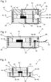
- Fig. 3 shows a cross-section view of an enclosure 10 formed by the glass substrate 12, the spacer substrate 16 and the cover substate 18.
- the three substrates 12, 16, 18 are bonded together via bond lines 26.
- the enclosure 1 hermetically encloses the function area 20 which receives the electrical device 22. Further the three substrates 12, 16 and 18 define a connector receptacle area 50 which allows the insertion of a suitable connector.
- Said connector receptacle area 50 is in electrical contact with the electrical device 22 by means of through glass vias 30 and conductive traces 36.
- the traces 36 are defined by structuring the electrically conductive coating 40 arranged on the respective outside facing surfaces of the glass substrate 12 and the cover substrate 18.
- the electrically conductive coating 40 arranged on the outside facing surfaces of the glass substrate 12 and the cover substrate 16 may be configured as a two-layer structure comprising the adhesion layer (42) and the barrier layer (44) as corrosion resistant layer.
- an upper contact 54 and a lower contact 56 are defined by structuring of the electrically conductive coating 40 arranged on the inside facing surfaces of the glass substrate 12 and the cover substrate 18. Further, for mechanically securing of a connector, connector notches 52 are formed in the glass substrate 12 and the cover substrate 18. The connector notches 52 are configured to receive latching elements of the connector.
- Figure 4 shows another enclosure 10, similar to the enclosure described with respect to figure 3 .
- the substrates 12, 16, 18 are configured to form a clamp 60 designed to receive and hold a nerve 62.
- the electrically conductive coating 40 is structured to form a contact pad 40 for electrically contacting the clamped nerve 62. This allows, for example, the nerve 62 to be in electrical contact with the electrical device 22 and to stimulate the nerve 62 by electrical pulses from the electrical device 22.
- Figure 5 shows another enclosure 10, where electrical contacts 34 are provided on the upper surface of the glass substrate 12 on either side of the enclosed function area 20.
- the two electrical contact pads 34 are obtained by structuring the electrically conductive coating 40.
- the respective electrical contact pads 34 are connected to the back side of the glass substrate 12 by through glass vias 30 and the electrical devices 22 is likewise connected to through glass vias 30.
- Conductive traces 36 formed on the outside facing surface of the glass substrate 12 by structuring of the electrically conductive coating 40 establish an electrical connection between two of the through glass vias 30.
- the electrically conductive coating 40 is structured such that the exposed surfaces of the conductive rods 32 of the through glass vias 30, see figure 2 , are covered by the coating 40.
- the arrangement shown in figure 5 allows the spacer substrate 16 as well as the cover substrate 18 to remain free from electrical contacts and through glass vias 30 while still providing access to the contact pads 34 from an upper side of the enclosure 1 via a free space 70 located above the contact pads 34.
- optical properties of the spacer substrate 16 and the cover substrate 18 are not impaired.
Landscapes
- Health & Medical Sciences (AREA)
- Animal Behavior & Ethology (AREA)
- Biomedical Technology (AREA)
- Nuclear Medicine, Radiotherapy & Molecular Imaging (AREA)
- Radiology & Medical Imaging (AREA)
- Life Sciences & Earth Sciences (AREA)
- Engineering & Computer Science (AREA)
- General Health & Medical Sciences (AREA)
- Public Health (AREA)
- Veterinary Medicine (AREA)
- Electrotherapy Devices (AREA)
- Micromachines (AREA)
- Joining Of Glass To Other Materials (AREA)
Abstract
Description
- The invention relates to a hermetic enclosure comprising at least one glass substrate having at least one electrical feedthrough configured as a through glass via which comprises a conductive rod electrically connecting the inside of the enclosure to the outside through a glass substrate.
- Electronic devices can be used inside the human body for sensing (e.g., temperature, fluid composition, pressure, conductivity, chemical properties, strain) or for active treatment (e.g., cardiovascular stimulation, nerve stimulation, brain stimulation, drug delivery, drug activation). However, electronic devices should not be placed directly in the human body. Since the body environment has an average pH-value from 7.35 to 7.45 and of a temperature 36.5-37.5 °C it is potentially corrosive. Ordinary metal and plastic components are likely to degrade in such an environment, releasing toxic substances. Usually, electronic devices used as implants are sealed in housings. Titanium or titanium alloy housings are widely used for cardiac stimulation. However, they are large, heavy and bulky if they are to be made hermetic. Glass as an enclosure material could be a lightweight but robust alternative. For example, European Patent
EP 3 012 059 B1 shows a method for manufacturing a transparent component for protecting an optical component. A new laser welding method is used therein. - Some electronic devices require housings having electrical feedthroughs in order to provide electrical connections to the outside.
EP 3 812 352 A1 discloses a hermetic glass enclosure with vias to establish an electrical contact from the inside of the enclosure to the outside, e.g., for contacting a contact pad at the outside of the enclosure. - Such Through Glass Vias (TGV) are made of metals, mostly tungsten, that connect the inside surface of the glass substrate with the outside surface. However, when subjected to a corrosive environment the materials of the through glass vias can corrode and can even be released out of the glass.
- It is thus an object of the invention to provide an improved electrical feedthrough through a glass substrate of a hermetic housing which is suitable for use in corrosive environments and in particular suitable for use as a medical implant.
- A hermetic enclosure comprising at least one glass substrate having at least one electrical feedthrough configured as a through glass via is proposed. The via comprises an electrically conductive rod electrically connecting the inside of the enclosure to the outside through the glass substrate. The part of the conductive rod's surface facing towards the outside of the enclosure is completely covered with an electrically conductive coating, wherein the electrically conductive coating is a multilayer structure comprising at least an adhesion layer in direct contact with the conductive rod and a corrosion resistant layer.
- Such hermetic enclosures are formed by two or more substrates which are hermetically bonded together to hermetically enclose a function area or a cavity. For example, the hermetic enclosure may comprise three substrates. A base formed by the glass substrate comprising the at least one electrical feedthrough, a spacer substate and a cover substrate. In this example, the base glass substrate defines a bottom wall of an enclosed cavity, the spacer substrate defines side walls of the enclosed cavity, and the cover substrate defines a top wall of the enclosed cavity. In a further example, the hermetic enclosure may comprise two substrates, a base glass substrate comprising the at least one electrical feedthrough, and a cavity substrate. The cavity substrate has a cavity produced, for example, by etching, laser assisted etching, CNC machining or laser ablation and defines side walls and a top wall of an enclosed cavity, and the base glass substrate defines a bottom wall of the enclosed cavity.
- The hermetic enclosure may be directly obtained by stacking the respective substrate and subsequently bonding of the substrates. An efficient method for obtaining a large number of hermetic enclosures involves stacking and bonding of entire wafers and subsequently separating the formed enclosures, e.g., by saw dicing. In one example, a spacer wafer comprises several openings which define the cavities in conjunction with adjacent base and cover wafers. In another example, individual cavities formed in a cavity wafer define the cavities in conjunction with an adjacent base wafer.
- Bonding of the substrates or wafers may, for example, be performed by means of laser bonding and/or laser welding, anodic bonding, fusion bonding, contact bonding or glass frit bonding. Bonding processes which allow direct bonding of two adjacent substrates or wafers without any intermediate material or adhesive material, such as laser bonding, are particularly preferred.
- The bonding is preferably performed such that a hermetic enclosure is formed, wherein the cavity or function area is enclosed within such an enclosure. As used herein, hermetically sealed means in particular an enclosure that has a helium leakage rate of less than 1·10-8 mbar·l/sec and is preferably in the range 1·10-10 mbar·l/sec to 1·10-9 mbar·l/sec.
- In a preferred laser bonding process, a short-pulsed laser beam from a laser source, for which at least one of the substrates is transparent, is focused to a spot inside the formed substrate stack. By choosing the repetition rate and a scan rate of the laser, the individual laser pulses are arranged so closely together that a resulting nonlinear absorption zone of a laser pulse within the material is in contact with a neighboring nonlinear absorption zone of a further laser pulse, or even overlaps with it, such that heat accumulation can occur. Due to the accumulated heat, the material of the substrate stack is locally melted and a continuous welding "line" can be obtained. For creating such a continuous welding line, a focus plane of the laser beam is arranged close to but not at the interface between the two substrates. The laser beam is arranged at a distance below the interface between the two substrates such that the accumulated heat causes the material of the first and second substrate to locally melt and mix so that a hermetic bond is formed. The area, in which the accumulated heat of the incident laser causes the material of the two substrates to melt and to mix is designated as laser treated zone. In an area surrounding said laser treated zone, the heat introduced by the laser is insufficient to melt the material but may cause modifications of the material and/or the electrically conductive coating arranged on the glass substrate. This area is in the following referred to as heat affected zone.
- Preferably, the glass substrate comprising the at least one electrical feedthrough is bonded to a further substrate, such as a spacer substrate or cavity substrate, by means of laser bonding, wherein at least one bond line is formed in which material of the glass substrate and the further substrate has been melted and mixed, wherein a distance between a laser bond line and a through glass via is preferably at least 50 µm. Additionally or alternatively, the distance between a laser bond line and a through glass via is chosen such that the through glass via is outside of the heat affected zone.
- The enclosed cavity provided by the proposed hermetic enclosure is in particular suited for housing an electronic device. The device is preferably electrically connected to the electrical feedthroughs and is thus capable of sending and/or receiving of electrical signals and/or electrical current from the outside of the hermetic enclosure.
- The electrical feedthroughs are configured as through glass vias and comprise conductive rods that are embedded in the glass substrate such that their front and back surfaces are accessible. Preferably, the conductive rods are made from or comprise metals like tungsten, titanium, an iron/nickel alloy, gold, silver, copper or (doped) silicon and combinations of said materials.
- A length of the conductive rods is chosen such that an electrical contact may be established through the glass substrate. A thickness of the glass substrate is preferably in the range of from 200 µm to 4000 µm, more preferably from 500 µm to 1000 µm. A length of the conductive rods is preferably in the range of from 200 µm to 4000 µm, more preferably from 500 µm to 1000 µm. The lengths of the conductive rods may be chosen to be identical to the thickness of the glass substrate.
- The material of the glass substrate is a glass that is preferably chosen from a borosilicate glass, such as BOROFLOAT® 33 or D263® T eco or MEMpax® available from SCHOTT AG, a quartz glass, fused silica, an alumino-borosilicate glass such as AF 32® available from SCHOTT AG, alkali-free glasses, SCHOTT B270@, or alkali-silicate glasses such as AS87.
- The materials of the further substrate(s), such as the spacer substrate, the cover substrate and/or the cavity substrate, are preferably selected from a glass, a glass ceramic, a ceramic, silicon, sapphire, diamond, or other inorganic crystals. Suitable glass materials include the materials described for the glass substrate. In case of a glass material, glasses suitable for the glass substrate are also suitable as material for the further substrate(s).
- In order to protect the electrical feedthroughs from damage, for example by corrosion, the electrically conductive coating in form of a multilayer structure is provided such that the material of the conductive rod(s) of the feedthrough(s) which is exposed on the outward facing side of the enclosure and thus of the outward facing side of the glass substrate is completely covered. Thus, an outward facing side of the conductive rod is covered which includes the front surface of the conductive rod facing towards the environment and which is not surrounded by the glass substrate and is thus exposed from the glass substrate. However, the inventors have found that it is not sufficient to apply a corrosion resistant coating layer to only said front surface of the conductive rod. For example, a gold coating arranged only on said front surface of a conductive rod made from tungsten will not reduce the corrosion. Instead, it has been surprisingly found that such a gold coating will even accelerate corrosion. In order to achieve the desired corrosion resistance, not only the front surface, but the entire exposed surface of the conductive rods must be completely covered. It is believed that accelerated corrosion, for example if the enclosure is subjected to an NaCl solution in water, is caused by electrochemical processes between the material of the coating and the material of the conductive rod.
- Accordingly, it is preferred to form the electrically conductive coating without any gaps such that the entire material of the conductive rod(s) which is exposed to the outside of the enclosure is covered and thus shielded from the environment. In order to achieve a gapless and complete coverage of the exposed surfaces of the metal rod(s), it is preferred to extend the electrically conductive coating to an area of the glass substrate surface adjacent to the respective conductive rod. This adjacent area preferably extends beyond the edge of the conductive rod for a distance of at least 1 µm, more preferred at least 2 µm, more preferred at least 5 µm, more preferred at least 10 µm and most preferred at least 40 µm. Since the accuracy of the patterning equipment also limits how well one can align and center the coating steps with respect to the conductive rods, it is preferred to choose the diameter of the contact pad dp greater than the diameter of the via dv; so dp = dv + Δd, with Δd > 5 µm, more preferred 10 µm, most preferred 20 µm or more. Without loss of generality, cylindrical conduction rods and conductive contact pads are assumed. In case those cross sections are not circular, dv= 2rmax, with rmax the maximum radius measured from the center of the via cross section and dp=2rmin, with rmin the minimum distance measured from the center of the of the contact pad cross section.
- In addition to application of the electrically conductive coating to an outward facing side, it is possible to also arrange the electrically conductive coating on an inside facing side of the conductive rods. Further, it is possible to extend the electrically conductive coating over a part of a surface of the substrate in order to form electrically conductive structures. In cases where the electrically conductive coating is applied on an inside facing side of the substate and/or the conductive rods, it is preferred that said coating covers the entire inside facing side of the conductive rod, but it is also possible to cover only a part of the conductive rod's front surface with the coating.
- The corrosion resistant contact layer provides both protection of the conductive rods from environmental influence and at the same time provides a reliable electrical contact surface for establishing an electrical connection. By means of this corrosion resistant contact layer, the hermetic enclosure may be used in corrosive environments including the animal and human body.
- The corrosion resistant contact layer provides a contact surface which may be used to establish permanent electrical connections, for example by means of soldering a wire to the contact surface. The contact surface may also be used as part of a connector or receptacle for establishing a disconnectable electrical connection.
- In case a solder connection is desired, the electrically conductive coating may be configured such that solder pads are formed.
- Preferably, the electrical feedthrough comprises a depression in or an elevation on an outside facing surface of the glass substrate and/or on an inside facing surface of the glass substrate, wherein the recess or elevation surrounds the electrically conductive rod, and wherein the recess or elevation is preferably flush with a front surface of the conductive rod, and wherein a depths of the depression or a height of the elevation is preferably at least 250 nm and/or less than 3 µm, preferably less than 2 µm, more preferably less than 500 nm.
- Choosing the depths/height of the depression/elevation and the lengths of the conductive rod such that the conductive rod's front surface is flush with the depression/elevation, allows for a flat and homogenous surface wherein the corrosion resistant conductive coating may extend seamlessly from the front surface of the conductive rod to a part of the surface of the glass substrate. A contact pad or solder pad formed by the coating may then be chosen to have a larger surface than the size of the front surface of the conductive rod, making it easier to establish an electrical connection.
- Preferably, the depths/height and/or shape of the recess or elevation are configured such that the recess or elevation serves as a flow boundary for solder. The depression or recess forms a boundary which influences and limits the flow of a solder material. If, for example, the entire area of the elevation or depression is covered with the electrically conductive coating, then the solder is only in contact with the formed solder pad and does not touch the glass substrate.
- The structuring of the glass substrate provided by the recess or elevation may also serve as anchor for the coating and may thus improve adhesion of the coating.
- Preferably, the electrically conductive coating is also arranged on at least a part of the glass substrate, wherein the electrically conductive coating forms a contact pad having a pad diameter dp which is larger than a via diameter dv of the conductive rod to which to contact pad is electrically connected.
- The electrically conductive coating may additionally or alternatively be configured to form at least one conductive trace. Such conductive traces may form electrical connections between one or more of the electrical feedthroughs, between an electrical feedthrough and a contact pad, or between two contact pads arranged on a surface of the glass substrate. A conductive trace may also be configured to form an antenna and/or coil structure. Such a structure may be arranged on an inside facing surface and/or an outside facing surface of a substrate of the enclosure.
- The electrically conductive coating is a multilayer structure having at least two layers. As the multilayer structure is electrically conductive, each of the layers is selected from an electrically conductive material.
- The corrosion resistant layer is preferably configured as a diffusion barrier layer and/or a corrosion resistant contact layer. It is possible that the electrically conductive coating comprises both a diffusion barrier layer and a corrosion resistant contact layer.
- Preferably, the multilayer structure of the electrically conductive coating comprises in this order the adhesion layer in direct contact with the conductive rod, at least one diffusion barrier layer, and the corrosion resistant contact layer.
- The adhesive layer is chosen such that it has good adhesion on the conductive rod's material and/or on the material of the glass substrate. Suitable adhesive layers are, for example, made from or comprise Ti, Ta, Cr, Ni, NiCr, TiAl and combinations thereof.
- A thickness of the adhesion layer is preferably in the range of from 2 nm to 200nm, more preferably from 10 nm to 150 nm and most preferably from 20 nm to 100 nm.
- The diffusion barrier layer is chosen such that diffusion of materials from the corrosion resistant contact layer or substances from outside of the hermetic enclosure cannot diffuse or propagate towards the conductive rods and vice versa. In particular, the diffusion barrier layer is chosen such that materials contained in a solder material or an adhesive material as well as oxygen from the environment cannot damage the conductive rods of the electrical feedthroughs. Further the material of the diffusion barrier layer is preferably chosen to be biocompatible. Biocompatible materials are non-toxic and have not injurious effects on biological systems.
- Preferably, the diffusion barrier layer is made from or comprises platinum (Pt), titan-nitride (TiN) and combinations thereof. If the diffusion barrier layer is the outermost layer of the multilayer structure, the material of the diffusion barrier layer is preferably chosen from a biocompatible material.
- A thickness of the diffusion barrier layer is preferably in the range of from 20 nm to 200nm, more preferably from 40 nm to 150 nm and most preferably from 50 nm to 100 nm.
- The corrosion resistant contact layer is preferably not only resistant to corrosive environments but is preferably also a material with good electrical conductivity and good wettability for solder materials in order to enable high quality electrical connections. Still further, as the corrosion resistant contact layer preferably forms the outermost layer of the electrically conductive coating, the corrosion resistant contact layer is preferably chosen from a biocompatible material.
- Preferably, the corrosion resistant contact layer is made from or comprises gold (Au).
- A thickness of the corrosion resistant contact layer is preferably in the range of from 50 nm to 200nm, more preferably from 80 nm to 150 nm and most preferably from 75 nm to 100 nm.
- The electrically conductive coating may in principle be applied to the surface of the conductive rods and optionally to a part of the glass substrate's surface by means of any suitable coating method. Preferably, at least one of the layers of the electrically conductive coating is obtained by means of electroplating, electroless plating, physical vapor deposition (PVD, e.g., sputtering or evaporation, in particular resistive evaporation), electron beam deposition and/or atomic layer deposition (ALD).
- Preferably, the corrosion resistant contact layer is a gold layer obtained by electroless plating. Such a process may employ the use of a seed layer to start an autocatalytic deposition of gold. Preferably, the adhesive layer or, if present, the diffusion barrier layer is chosen such that said layer serves as seed layer so that no additional seed layer is required.
- Preferably, the material of the glass substrate and/or the electrically conductive coating are selected such that said materials are resistant to exposure to an NaCl solution in water, in particular to a solution of 700g/l NaCl. The enclosure may, for example, be immersed in such a solution for seven days at a temperature of 37°C and may then be examined visually for signs of corrosion. Further, it is possible to assess the corrosion resistance by determining a loss of mass. A material may then be considered to be corrosion resistant if the loss of mass is less than 5%, preferably less than 3% and most preferably less than 1%. The total mass of the electrically conductive coating is a small quantity so that a loss of mass of the material of the electrically conducting coating is hard to measure. However, if the coating is not resistant, it will develop gaps after exposure with a corrosive environment and said gaps will lead to an exposure of the conductive rods to the NaCl solution. Accordingly, the material of the electrically conductive coating is in particular considered to be corrosion resistant, if the conductive rods remain protected and thus an overall mass loss of the material of the conductive rods after exposure of the enclosure to an NaCl solution in water with 700g/l NaCl at a temperature of 37 °C for 7 days, is preferably less than 5%, more preferably less than 3% and most preferred less than 1%. Further, for the material of the glass substrate it is preferred that the mass loss of the material of the glass substrate is less than 5%, preferably less than 3% and more preferably less than 1%.
- As the loss of mass of a conductive rod is a small quantity, it is preferred to use an ensemble of several enclosures to test for corrosion resistance. For example, if the enclosure has V conductive rods of mass mr, an ensemble of N enclosures is used so that the total mass of the conduction rods is larger than 0.1 g:

- The measurement may then be performed by first drying the samples, for example in in a drying cabinet using IR-drying at 100°C for 30 min. After drying, the initial weight M0 of the dry ensemble is determined, for example by means of an analytical balance (e.g., VWRI 611-3350 / LA314i from Avantor). The ensemble of enclosures is then immersed in NaCl -solution (700 g/l) for seven days at 37°C. After the testing period, the samples are rinsed with de-ionzed water and then dried, for example in a drying cabinet (IR-drying, 100°C for 30 min). After drying, the weight M1 of the dry ensemble is determined, for example by means of an analytical balance (e.g., VWRI 611-3350 / LA314i from Avantor).
- Hence, ΔM = M0 - M1 and ΔM/Mr < 5%, < 3%, most preferred less than 1%.
- In order to discriminate, whether the loss in mass results from loss of mass of the conductive rods or from a corrosion of the glass (which should also be avoided), the test may be repeated on a matching ensemble using the same method with glass enclosures of the same spatial dimensions and of the same glass but with no though glass vias and thus without conductive rods. A difference in the determined mass losses ΔM between these two measurements yields the mass loss of the material of the conductive rods.
- The structure of the electrically conductive coating is summarized in table 1.
(Table 1, coating properties) Layer Thickness / length function Preferred material Conductive rod 200 µm to 4 mm electrical conductor through glass substrate Tungsten, iron/nickel alloy, Gold, Silver, Copper, Titanium, (doped) silicon Adhesion layer 2 nm to 200 nm promotes adhesion between coating and conductive rod and/or glass substrate Ti, Ta, Cr, Ni or alloys of those metals, such as NiCr, TiAl Corrosion resistant Diffusion barrier 20 nm to 200 nm biocompatible diffusion barrier to prevent oxidation of conductive rod Pt, TiN Optional corrosion resistant contact layer 50 nm to 2000 nm inert outside facing layer with good wetting by solder Gold - Examples for suitable coatings applied to a glass substrate having through glass vias are given in table 2 below.
(Table 2, examples for coatings on glass substrates with through glass vias) Example 1 Example 2 Example 3 Glass substrate Boro33 ©: 1500 µm Boro33 ©: 500 µm Fused silica: 100 µm Conductive rod Tungsten: 1500 µm Tungsten: 500 µm Copper: 100 µm Adhesion layer Titanium: 70 nm Titanium: 100 nm Nickel 50 nm Corrosion resistant Diffusion barrier Platinum: 70 nm Platinum: 200 nm Platinum: 50 nm Optional corrosion resistant contact layer Gold: 200 nm - Gold: 200 nm - The enclosure may comprise more than one substrate made from a glass and having at least one through glass via. For example, not only the base substrate, but also the cover substrate may be configured as a glass substrate having feedthroughs protected by the electrically conductive coating having a corrosion resistant layer.
- A further aspect of the invention can be seen in providing a method for producing the hermetic enclosure described herein. The method comprises providing a glass substrate having at least one electrical feedthrough configured as a through glass via and subsequent coating of a surface of the glass substrate with an electrically conductive coating. After the coating, an optional step of selectively removing the electrically conductive coating in areas between two or more through glass vias to form contact pads or to structure conductive traces may be performed.
- The glass substrate is hermetically bonded to a further substrate, preferably by means of laser bonding wherein at least one bond line is formed in which material of the glass substrate and the further substrate has been melted and mixed. For laser bonding, at least one laser weld line is preferably made using an ultrashort pulse laser. Typical pulse widths are in the range of 100 fs to 100 ps. A method for carrying out such a laser bond with one or more laser welding lines is known, for example, from
EP 3 012 059 B1 . - The steps of coating and hermetic bonding can be performed in any order.
- The hermetic enclosure described herein is in particular suitable for use as a housing for medical implants. Accordingly, a medical implant is provided comprising one of the hermetic enclosures described herein.
- It is understood that the above-mentioned features and those to be explained below can be used not only in the respective combination as shown, but also in other combinations or on their own, without leaving the scope of the present invention.
- Preferred embodiments of the invention are shown in the figures and will be explained in more detail in the following description, wherein identical reference numerals refer to identical or similar components or elements.
- The figures show in schematic form:
- Figure 1
- a schematic cross section view from the side of a hermetic enclosure with coated through glass vias,
- Figure 2
- an enlarged cross-section side view of a through glass via,
- Figure 3
- an enclosure having a connector receptacle,
- Figure 4
- an enclosure comprising a clamp mechanism, and
- Figure 5
- an enclosure with contact pads on the opposite side of the through contacts.
-
Figure 1 shows ahermetic enclosure 10 with throughglass vias 30 in a schematic side view. Theenclosure 10 is formed by aglass substrate 12 comprising the throughglass vias 30 and further substrates 14. - In the example depicted in
figure 1 , thebase glass substrate 12 forms the bottom of theenclosure 10. A spacer substrate 16 as a first further substrate 14 forms side walls of the enclosure 1 and acover substrate 18 as second further substrate 14 forms a top wall of theenclosure 10. Theenclosure 10 defines a cavity orfunction area 20. - In order to ensure that the
function area 20 is hermetically enclosed, theglass substrate 12 is hermetically bonded to the spacer substrate 16 and the spacer substrate 16 is hermetically bonded to thecover substrate 18 by means of a laser bonding process. In said laser bonding process, the material at the interface of the tworespective substrates function area 20. - In the example shown in
figure 1 , anelectrical device 22 is located in thefunction area 20 and is thus enclosed by theenclosure 10. In order to establish an electrical connection to the outside of theenclosure 10, theelectrical device 22 is arranged over the throughglass vias 30 and is electrically connected to said throughglass vias 30 by means of a solder connection formed by solder drops 24. It is of course also possible to use other means to connect theelectrical device 22 to the throughglass vias 30. For example, theelectrical device 22 may be located next to the throughglass vias 30 on theglass substrate 12 and bond wires may be used to connect theelectrical device 30 to the throughglass vias 30. - For corrosion protection, an electrically
conductive coating 40 configured ascontact pads 34 is arranged on the outside facing side of the throughglass vias 30. The detailed structure of the throughglass vias 30 and thecoating 40 is further described with respect tofigure 2 . -
Figure 2 shows an enlarged cross-section side view of a through glass via 30 of thehermetic enclosure 10 shown infigure 1 . The through glass via 30 comprises a metal rod as electricallyconductive rod 32 which is arranged such that a front surface of theconductive rod 32 is flush with an inside facing surface of theglass substrate 12. A further front surface of theconductive rod 32 is flush with an outside facing surface of theglass substrate 12. This allows theconductive rod 32 to provide an electrically conductive connection from the inside of theenclosure 10 to the outside. - For corrosion protection of the through glass via 30 and in particular for corrosion protection of the
conductive rod 32, the electricallyconductive coating 40 is arranged on the outside facing front side of theconductive rod 32 and a part of the outside facing surface of theglass substrate 12. - The electrically
conductive coating 40 is in the depicted embodiment configured as a layer structure having in this order anadhesion layer 42, adiffusion barrier layer 44 and a corrosionresistant contact layer 46. Thecoating 40 is structured to form acontact pad 34 having a diameter dp which is larger than a diameter dv of theconductive rod 32 of the through glass via 30. The material of the corrosionresistant contact layer 46 is in this example a material with good wettability for solder materials such as gold (Au). - In the layer structure of the example depicted in
figure 2 , the outermost layer is the corrosionresistant contact layer 46. The material of said corrosionresistant contact layer 46 is selected such that it can withstand a defined corrosive environment, such as a NaCl solution. - In an alternative embodiment, where no solder connection is required, the diffusion barrier layer can be selected from a corrosion resistant electrically conductive material and may thus serve as outermost layer.
- The diffusion barrier layer is selected from a material such as platinum (Pt) which prevents diffusion of substances from the outside environment into the material of the
conductive rod 32 and vice versa. In particular, the diffusion barrier layer is chosen such that it prevents diffusion of oxygen into the material of theconductive rods 32. - In this embodiment, the electrically
conductive coating 40 is both arranged on the outside facing side as well as on the inside facing side of theglass substrate 12. The electricallyconductive coating 40 on the inside facing side serves as acontact pad 34 for thesolder drop 24 which electrically connects theelectrical device 22, seefigure 1 , to the through glass via 30. - In further embodiments, a part of the surface of the
glass substrate 12 surrounding theconductive rod 32 could be raised or lowered compared to the remaining surface of theglass substrate 12 to form an elevation or depression surrounding theconductive rod 32. The raised or lowered area is preferably flush with the end surface of theconductive rod 32. Preferably, the electricallyconductive coating 40 forming thecontact pad 34 covers the entire area of said elevation or depression. Such an elevation or depression may be applied to control the flow of a solder material, wherein preferably said solder material would be confined to the elevation or depression. - The corrosion-resistant properties of the electrically
conductive coating 40 are not required on the inside facing surface as theenclosure 10 protects theenclosed function area 20 from any corrosive influence from the outside. However, having the same electricallyconductive coating 40 on both surfaces allows the use of the same coating process and results in asymmetrical glass substrate 12 so that any of the two sides may face towards the spacer substrate 16. -
Fig. 3 shows a cross-section view of anenclosure 10 formed by theglass substrate 12, the spacer substrate 16 and thecover substate 18. The threesubstrates function area 20 which receives theelectrical device 22. Further the threesubstrates connector receptacle area 50 which allows the insertion of a suitable connector. - Said
connector receptacle area 50 is in electrical contact with theelectrical device 22 by means of throughglass vias 30 and conductive traces 36. Thetraces 36 are defined by structuring the electricallyconductive coating 40 arranged on the respective outside facing surfaces of theglass substrate 12 and thecover substrate 18. - As it is not intended to form a solder connection to the conductive traces 36, the electrically
conductive coating 40 arranged on the outside facing surfaces of theglass substrate 12 and the cover substrate 16 may be configured as a two-layer structure comprising the adhesion layer (42) and the barrier layer (44) as corrosion resistant layer. - Within the
connector receptacle area 50, an upper contact 54 and a lower contact 56 are defined by structuring of the electricallyconductive coating 40 arranged on the inside facing surfaces of theglass substrate 12 and thecover substrate 18. Further, for mechanically securing of a connector,connector notches 52 are formed in theglass substrate 12 and thecover substrate 18. Theconnector notches 52 are configured to receive latching elements of the connector. -
Figure 4 shows anotherenclosure 10, similar to the enclosure described with respect tofigure 3 . In contrast to the embodiment offigure 3 , thesubstrates clamp 60 designed to receive and hold anerve 62. - Within the
clamp 60, the electricallyconductive coating 40 is structured to form acontact pad 40 for electrically contacting the clampednerve 62. This allows, for example, thenerve 62 to be in electrical contact with theelectrical device 22 and to stimulate thenerve 62 by electrical pulses from theelectrical device 22. -
Figure 5 shows anotherenclosure 10, whereelectrical contacts 34 are provided on the upper surface of theglass substrate 12 on either side of theenclosed function area 20. The twoelectrical contact pads 34 are obtained by structuring the electricallyconductive coating 40. The respectiveelectrical contact pads 34 are connected to the back side of theglass substrate 12 by throughglass vias 30 and theelectrical devices 22 is likewise connected to throughglass vias 30. Conductive traces 36 formed on the outside facing surface of theglass substrate 12 by structuring of the electricallyconductive coating 40 establish an electrical connection between two of the throughglass vias 30. The electricallyconductive coating 40 is structured such that the exposed surfaces of theconductive rods 32 of the throughglass vias 30, seefigure 2 , are covered by thecoating 40. - The arrangement shown in
figure 5 allows the spacer substrate 16 as well as thecover substrate 18 to remain free from electrical contacts and throughglass vias 30 while still providing access to thecontact pads 34 from an upper side of the enclosure 1 via afree space 70 located above thecontact pads 34. Thus, optical properties of the spacer substrate 16 and thecover substrate 18 are not impaired. - Although the present invention has been described with reference to preferred examples of embodiments, it is not limited thereto but can be modified in a variety of ways.
-
- 10
- enclosure
- 12
- glass substrate
- 14
- further substrate
- 16
- spacer substrate
- 18
- cover substrate
- 20
- function area
- 22
- electrical device
- 24
- solder drop
- 26
- bond line
- 30
- through glass via
- 32
- conductive rod
- 34
- contact pad
- 36
- trace
- 40
- conductive coating
- 42
- adhesion layer
- 44
- diffusion barrier layer
- 46
- contact layer
- 50
- connector receptacle area
- 52
- connector notch
- 54
- upper contact
- 56
- lower contact
- 60
- clamp
- 62
- nerve
- 70
- free space
- dv
- diameter through glass via
- dp
- diameter contact pad
Claims (15)
- Hermetic enclosure (10) comprising at least one glass substrate (12) having at least one electrical feedthrough configured as a through glass via (30), the through glass via (30) comprising a conductive rod (32) electrically connecting the inside of the hermetic enclosure (10) to the outside through the glass substrate (12), characterized in that the part of the conductive rod's (32) surface facing towards the outside of the hermetic enclosure (10) is completely covered with an electrically conductive coating (40), wherein the electrically conductive coating (40) is a multilayer structure comprising at least an adhesion layer (42) in direct contact with the conductive rod (32) and a corrosion resistant layer.
- Hermetic enclosure (10) according to claim 1, characterized in that the electrical feedthrough comprises a depression in or an elevation on an outside facing surface of the glass substrate (12) and/or on an inside facing surface of the glass substrate (12), wherein the recess or elevation surrounds the conductive rod (32), and wherein the recess or elevation is preferably flush with a front surface of the conductive rod (32), and wherein a depths of the depression or a height of the elevation is preferably at least 250 nm and/or less than 3 µm.
- Hermetic enclosure (10) according to claim 2, characterized in that the depths/height and/or shape of the recess or elevation are configured such that the recess or elevation serves as a flow boundary for solder, preferably such that the solder does not touch the glass substrate (12).
- Hermetic enclosure (10) according to any one of claims 1 to 3, characterized in that the corrosion resistant layer is configured as diffusion barrier layer (44) and/or a corrosion resistant contact layer (46), wherein the multilayer structure of the electrically conductive coating (40) preferably comprises in this order the adhesion layer (42) in direct contact with the conductive rod (32), at least one diffusion barrier layer(44) and a corrosion resistant contact layer (46).
- Hermetic enclosure (10) according to claim 4, characterized in that the adhesive layer (42) is made from or comprises Ti, Ta, Cr, Ni, NiCr, TiAl and combinations thereof.
- Hermetic enclosure (10) according to claim 4 or 5, characterized in that the diffusion barrier layer (44) is made from or comprises platinum (Pt), titan-nitride (TiN) and combinations thereof.
- Hermetic enclosure (10) according to any one of claims 1 to 6, characterized in that the corrosion resistant contact layer (46) is made from or comprises gold (Au).
- Hermetic enclosure (10) according to any one of claims 1 to 7, characterized in that the conductive rods (32) are made from or comprise tungsten, titanium, an iron/nickel alloy, gold, silver, copper, silicon, and combinations of said materials.
- Hermetic enclosure (10) according to any one of claims 1 to 8, characterized in that the electrically conductive coating (40) is also arranged on at least a part of a surface the glass substrate (12), wherein the electrically conductive coating (40) forms a contact pad (34) having a pad diameter dp which is larger than a via diameter dv of the conductive rod (32) to which to contact pad (34) is electrically connected, and/or
wherein the electrically conductive coating (40) forms at least one conductive trace (36) which preferably electrically connects two or more through glass vias (30). - Hermetic enclosure (10) according to any one of claims 1 to 9, characterized in that at least one of the layers of the electrically conductive coating (40) is obtained by means of electroplating, electroless plating, physical vapor deposition (PVD), electron beam deposition and/or atomic layer deposition (ALD).
- Hermetic enclosure (10) according to any one of claims 1 to 10, characterized in that the corrosion resistant contact layer (46) is a gold layer obtained by electroless plating.
- Hermetic enclosure (10) according to any one of claims 1 to 11, characterized in that the glass substrate (12) is bonded to a further substrate (14) by means of laser bonding and/or laser welding, wherein at least one bond line (26) is formed in which material of the glass substrate (12) and the further substrate (14) has been melted and mixed, wherein a distance between a laser bond line (26) and a through glass via (30) is at least 50 µm.
- Hermetic enclosure (10) according to any one of claims 1 to 12, characterized that the material of the glass substrate (12) and the corrosion resistant layer of the electrically conductive coating (40) are selected such that the material is resistant to exposure to an NaCl solution in water of 700 g/l NaCl at a temperature of 37°C for 7 days.
- Method for producing a hermetic enclosure (10) according to any one of claims 1 to 13, comprising the steps of- providing a glass substrate (12) having at least one electrical feedthrough configured as a through glass via (30),- coating of a surface of the glass substrate (12) with an electrically conductive coating (40) and optionally subsequently selectively removing the electrically conductive coating (40) in areas between two or more through glass vias (30) to form contact pads (40) and/or conductive traces (36),- hermetic bonding of the glass substrate (12) to a further substrate (14) by means of laser bonding wherein at least one bond line (26) is formed in which material of the glass substrate (12) and the further substrate (14) has been melted and mixed,wherein the steps of coating and hermetic bonding can be performed in any order.
- Medical implant comprising a hermetic enclosure (10) according to any one of claims 1 to 14 or obtained by the method of claim 15.
Priority Applications (5)
| Application Number | Priority Date | Filing Date | Title |
|---|---|---|---|
| EP23184167.7A EP4487903B1 (en) | 2023-07-07 | 2023-07-07 | Hermetic enclosure comprising through glass vias and medical implant compris-ing such a hermetic enclosure |
| FIEP23184167.7T FI4487903T3 (en) | 2023-07-07 | 2023-07-07 | Hermetic enclosure comprising through glass vias and medical implant compris-ing such a hermetic enclosure |
| AU2024295939A AU2024295939A1 (en) | 2023-07-07 | 2024-07-01 | Hermetic enclosure comprising through glass vias and medical implant comprising such a hermetic enclosure |
| CN202480045242.4A CN121443355A (en) | 2023-07-07 | 2024-07-01 | Including a hermetically sealed housing with glass through-holes and a medical implant including the hermetically sealed housing. |
| PCT/EP2024/068461 WO2025012001A1 (en) | 2023-07-07 | 2024-07-01 | Hermetic enclosure comprising through glass vias and medical implant comprising such a hermetic enclosure |
Applications Claiming Priority (1)
| Application Number | Priority Date | Filing Date | Title |
|---|---|---|---|
| EP23184167.7A EP4487903B1 (en) | 2023-07-07 | 2023-07-07 | Hermetic enclosure comprising through glass vias and medical implant compris-ing such a hermetic enclosure |
Publications (2)
| Publication Number | Publication Date |
|---|---|
| EP4487903A1 true EP4487903A1 (en) | 2025-01-08 |
| EP4487903B1 EP4487903B1 (en) | 2025-06-04 |
Family
ID=87196247
Family Applications (1)
| Application Number | Title | Priority Date | Filing Date |
|---|---|---|---|
| EP23184167.7A Active EP4487903B1 (en) | 2023-07-07 | 2023-07-07 | Hermetic enclosure comprising through glass vias and medical implant compris-ing such a hermetic enclosure |
Country Status (5)
| Country | Link |
|---|---|
| EP (1) | EP4487903B1 (en) |
| CN (1) | CN121443355A (en) |
| AU (1) | AU2024295939A1 (en) |
| FI (1) | FI4487903T3 (en) |
| WO (1) | WO2025012001A1 (en) |
Citations (5)
| Publication number | Priority date | Publication date | Assignee | Title |
|---|---|---|---|---|
| US7812416B2 (en) * | 2006-05-22 | 2010-10-12 | Cardiomems, Inc. | Methods and apparatus having an integrated circuit attached to fused silica |
| US20140343648A1 (en) * | 2011-11-23 | 2014-11-20 | Heraeus Precious Metals Gmbh & Co., Kg | Contacting arrangement comprising a feedthrough and a filter structure and method of making |
| EP3012059B1 (en) | 2014-09-26 | 2017-10-18 | Primoceler Oy | Method to produce a transparent piece to be used to protect an optical component |
| EP3812352A1 (en) | 2019-10-24 | 2021-04-28 | Schott Primoceler Oy | Glass compound arrangement |
| US20210304973A1 (en) * | 2020-03-27 | 2021-09-30 | Menlo Microsystems, Inc. | MEMS Device Built On Substrate With Ruthenium Based Contact Surface Material |
-
2023
- 2023-07-07 EP EP23184167.7A patent/EP4487903B1/en active Active
- 2023-07-07 FI FIEP23184167.7T patent/FI4487903T3/en active
-
2024
- 2024-07-01 AU AU2024295939A patent/AU2024295939A1/en active Pending
- 2024-07-01 WO PCT/EP2024/068461 patent/WO2025012001A1/en not_active Ceased
- 2024-07-01 CN CN202480045242.4A patent/CN121443355A/en active Pending
Patent Citations (5)
| Publication number | Priority date | Publication date | Assignee | Title |
|---|---|---|---|---|
| US7812416B2 (en) * | 2006-05-22 | 2010-10-12 | Cardiomems, Inc. | Methods and apparatus having an integrated circuit attached to fused silica |
| US20140343648A1 (en) * | 2011-11-23 | 2014-11-20 | Heraeus Precious Metals Gmbh & Co., Kg | Contacting arrangement comprising a feedthrough and a filter structure and method of making |
| EP3012059B1 (en) | 2014-09-26 | 2017-10-18 | Primoceler Oy | Method to produce a transparent piece to be used to protect an optical component |
| EP3812352A1 (en) | 2019-10-24 | 2021-04-28 | Schott Primoceler Oy | Glass compound arrangement |
| US20210304973A1 (en) * | 2020-03-27 | 2021-09-30 | Menlo Microsystems, Inc. | MEMS Device Built On Substrate With Ruthenium Based Contact Surface Material |
Also Published As
| Publication number | Publication date |
|---|---|
| WO2025012001A1 (en) | 2025-01-16 |
| FI4487903T3 (en) | 2025-09-01 |
| CN121443355A (en) | 2026-01-30 |
| AU2024295939A1 (en) | 2026-01-08 |
| EP4487903B1 (en) | 2025-06-04 |
Similar Documents
| Publication | Publication Date | Title |
|---|---|---|
| CA2229596C (en) | Hermetically sealed electrical feedthrough for use with implantable electronic devices | |
| US8013433B2 (en) | Virtual wire assembly having hermetic feedthroughs | |
| US6759309B2 (en) | Micromachined structures including glass vias with internal conductive layers anodically bonded to silicon-containing substrates | |
| US9782111B2 (en) | Hermetic feedthrough assembly for ceramic body | |
| US20050219787A1 (en) | EMI filter capacitors designed for direct body fluid exposure | |
| US20070260282A1 (en) | Feedthrough apparatus with noble metal-coated leads | |
| CN103842024A (en) | Method for interconnecting conductors and feedthroughs with pads of sufficient thickness | |
| CN112023267A (en) | Glass-metal feed-through with sleeve | |
| EP4487903B1 (en) | Hermetic enclosure comprising through glass vias and medical implant compris-ing such a hermetic enclosure | |
| JP2009545729A (en) | Manufacturing method of temperature sensor | |
| EP1255972B2 (en) | Temperature sensor and a method for bonding a temperature sensor | |
| WO2005008853A1 (en) | Surge absorber | |
| JP4647505B2 (en) | Structure, wiring board, and method of manufacturing structure with wiring | |
| TWI381505B (en) | Lead frame and method for manufacturing semiconductor package using the same | |
| DE102010036217B4 (en) | Method for the hermetic encapsulation of a microsystem | |
| EP3517944A1 (en) | Measurement unit for an ion-sensitive solid-state electrode and ion-sensitive electrode | |
| EP3517943A1 (en) | Ion-sensitive glass electrode, measurement unit and method for manufacturing | |
| Langenmair et al. | Low-temperature sealing of titanium for hermetic implant packages | |
| Kohler et al. | Reliability investigations and improvements of interconnection technologies for the wireless brain-machine interface—‘BrainCon’ | |
| Knudsen et al. | A high‐reliability alumina‐platinum multilayer system for implantable medical devices | |
| EP4678222A1 (en) | Implantable device | |
| WO2023129538A1 (en) | Electrical component and method of forming same | |
| JP3752471B2 (en) | Semiconductor element storage package and semiconductor device | |
| US20090298286A1 (en) | Method of making electronic entities | |
| US20250065135A1 (en) | Enclosures with hermetic feedthroughs |
Legal Events
| Date | Code | Title | Description |
|---|---|---|---|
| STAA | Information on the status of an ep patent application or granted ep patent |
Free format text: STATUS: EXAMINATION IS IN PROGRESS |
|
| PUAI | Public reference made under article 153(3) epc to a published international application that has entered the european phase |
Free format text: ORIGINAL CODE: 0009012 |
|
| 17P | Request for examination filed |
Effective date: 20230707 |
|
| AK | Designated contracting states |
Kind code of ref document: A1 Designated state(s): AL AT BE BG CH CY CZ DE DK EE ES FI FR GB GR HR HU IE IS IT LI LT LU LV MC ME MK MT NL NO PL PT RO RS SE SI SK SM TR |
|
| REG | Reference to a national code |
Ref country code: DE Ref legal event code: R079 Free format text: PREVIOUS MAIN CLASS: A61N0001375000 Ipc: H01L0023055000 Ref document number: 602023003801 Country of ref document: DE |
|
| GRAP | Despatch of communication of intention to grant a patent |
Free format text: ORIGINAL CODE: EPIDOSNIGR1 |
|
| STAA | Information on the status of an ep patent application or granted ep patent |
Free format text: STATUS: GRANT OF PATENT IS INTENDED |
|
| RIC1 | Information provided on ipc code assigned before grant |
Ipc: H01L 23/10 20060101ALI20250108BHEP Ipc: A61N 1/375 20060101ALI20250108BHEP Ipc: H01L 23/055 20060101AFI20250108BHEP |
|
| INTG | Intention to grant announced |
Effective date: 20250127 |
|
| GRAS | Grant fee paid |
Free format text: ORIGINAL CODE: EPIDOSNIGR3 |
|
| GRAA | (expected) grant |
Free format text: ORIGINAL CODE: 0009210 |
|
| STAA | Information on the status of an ep patent application or granted ep patent |
Free format text: STATUS: THE PATENT HAS BEEN GRANTED |
|
| P01 | Opt-out of the competence of the unified patent court (upc) registered |
Free format text: CASE NUMBER: APP_17052/2025 Effective date: 20250408 |
|
| AK | Designated contracting states |
Kind code of ref document: B1 Designated state(s): AL AT BE BG CH CY CZ DE DK EE ES FI FR GB GR HR HU IE IS IT LI LT LU LV MC ME MK MT NL NO PL PT RO RS SE SI SK SM TR |
|
| REG | Reference to a national code |
Ref country code: GB Ref legal event code: FG4D |
|
| REG | Reference to a national code |
Ref country code: CH Ref legal event code: EP |
|
| REG | Reference to a national code |
Ref country code: DE Ref legal event code: R096 Ref document number: 602023003801 Country of ref document: DE |
|
| REG | Reference to a national code |
Ref country code: IE Ref legal event code: FG4D |
|
| REG | Reference to a national code |
Ref country code: FI Ref legal event code: FGE |
|
| REG | Reference to a national code |
Ref country code: NL Ref legal event code: MP Effective date: 20250604 |
|
| PG25 | Lapsed in a contracting state [announced via postgrant information from national office to epo] |
Ref country code: ES Free format text: LAPSE BECAUSE OF FAILURE TO SUBMIT A TRANSLATION OF THE DESCRIPTION OR TO PAY THE FEE WITHIN THE PRESCRIBED TIME-LIMIT Effective date: 20250604 |
|
| PGFP | Annual fee paid to national office [announced via postgrant information from national office to epo] |
Ref country code: FI Payment date: 20250822 Year of fee payment: 3 |
|
| PGFP | Annual fee paid to national office [announced via postgrant information from national office to epo] |
Ref country code: DE Payment date: 20250722 Year of fee payment: 3 |
|
| REG | Reference to a national code |
Ref country code: LT Ref legal event code: MG9D |
|
| PG25 | Lapsed in a contracting state [announced via postgrant information from national office to epo] |
Ref country code: NO Free format text: LAPSE BECAUSE OF FAILURE TO SUBMIT A TRANSLATION OF THE DESCRIPTION OR TO PAY THE FEE WITHIN THE PRESCRIBED TIME-LIMIT Effective date: 20250904 Ref country code: GR Free format text: LAPSE BECAUSE OF FAILURE TO SUBMIT A TRANSLATION OF THE DESCRIPTION OR TO PAY THE FEE WITHIN THE PRESCRIBED TIME-LIMIT Effective date: 20250905 |
|
| PG25 | Lapsed in a contracting state [announced via postgrant information from national office to epo] |
Ref country code: PL Free format text: LAPSE BECAUSE OF FAILURE TO SUBMIT A TRANSLATION OF THE DESCRIPTION OR TO PAY THE FEE WITHIN THE PRESCRIBED TIME-LIMIT Effective date: 20250604 |
|
| PG25 | Lapsed in a contracting state [announced via postgrant information from national office to epo] |
Ref country code: BG Free format text: LAPSE BECAUSE OF FAILURE TO SUBMIT A TRANSLATION OF THE DESCRIPTION OR TO PAY THE FEE WITHIN THE PRESCRIBED TIME-LIMIT Effective date: 20250604 |
|
| PG25 | Lapsed in a contracting state [announced via postgrant information from national office to epo] |
Ref country code: HR Free format text: LAPSE BECAUSE OF FAILURE TO SUBMIT A TRANSLATION OF THE DESCRIPTION OR TO PAY THE FEE WITHIN THE PRESCRIBED TIME-LIMIT Effective date: 20250604 |
|
| PGFP | Annual fee paid to national office [announced via postgrant information from national office to epo] |
Ref country code: AT Payment date: 20251020 Year of fee payment: 3 Ref country code: FR Payment date: 20250730 Year of fee payment: 3 |
|
| PG25 | Lapsed in a contracting state [announced via postgrant information from national office to epo] |
Ref country code: RS Free format text: LAPSE BECAUSE OF FAILURE TO SUBMIT A TRANSLATION OF THE DESCRIPTION OR TO PAY THE FEE WITHIN THE PRESCRIBED TIME-LIMIT Effective date: 20250904 |
|
| PG25 | Lapsed in a contracting state [announced via postgrant information from national office to epo] |
Ref country code: LV Free format text: LAPSE BECAUSE OF FAILURE TO SUBMIT A TRANSLATION OF THE DESCRIPTION OR TO PAY THE FEE WITHIN THE PRESCRIBED TIME-LIMIT Effective date: 20250604 |
|
| PG25 | Lapsed in a contracting state [announced via postgrant information from national office to epo] |
Ref country code: NL Free format text: LAPSE BECAUSE OF FAILURE TO SUBMIT A TRANSLATION OF THE DESCRIPTION OR TO PAY THE FEE WITHIN THE PRESCRIBED TIME-LIMIT Effective date: 20250604 |
|
| REG | Reference to a national code |
Ref country code: DE Ref legal event code: R079 Ref document number: 602023003801 Country of ref document: DE Free format text: PREVIOUS MAIN CLASS: H01L0023055000 Ipc: H10W0076153000 |
|
| PG25 | Lapsed in a contracting state [announced via postgrant information from national office to epo] |
Ref country code: PT Free format text: LAPSE BECAUSE OF FAILURE TO SUBMIT A TRANSLATION OF THE DESCRIPTION OR TO PAY THE FEE WITHIN THE PRESCRIBED TIME-LIMIT Effective date: 20251006 |
|
| REG | Reference to a national code |
Ref country code: AT Ref legal event code: MK05 Ref document number: 1801240 Country of ref document: AT Kind code of ref document: T Effective date: 20250604 |
|
| PG25 | Lapsed in a contracting state [announced via postgrant information from national office to epo] |
Ref country code: IS Free format text: LAPSE BECAUSE OF FAILURE TO SUBMIT A TRANSLATION OF THE DESCRIPTION OR TO PAY THE FEE WITHIN THE PRESCRIBED TIME-LIMIT Effective date: 20251004 |
|
| PG25 | Lapsed in a contracting state [announced via postgrant information from national office to epo] |
Ref country code: AT Free format text: LAPSE BECAUSE OF FAILURE TO SUBMIT A TRANSLATION OF THE DESCRIPTION OR TO PAY THE FEE WITHIN THE PRESCRIBED TIME-LIMIT Effective date: 20250604 Ref country code: SM Free format text: LAPSE BECAUSE OF FAILURE TO SUBMIT A TRANSLATION OF THE DESCRIPTION OR TO PAY THE FEE WITHIN THE PRESCRIBED TIME-LIMIT Effective date: 20250604 |
|
| PG25 | Lapsed in a contracting state [announced via postgrant information from national office to epo] |
Ref country code: CZ Free format text: LAPSE BECAUSE OF FAILURE TO SUBMIT A TRANSLATION OF THE DESCRIPTION OR TO PAY THE FEE WITHIN THE PRESCRIBED TIME-LIMIT Effective date: 20250604 |
|
| PG25 | Lapsed in a contracting state [announced via postgrant information from national office to epo] |
Ref country code: EE Free format text: LAPSE BECAUSE OF FAILURE TO SUBMIT A TRANSLATION OF THE DESCRIPTION OR TO PAY THE FEE WITHIN THE PRESCRIBED TIME-LIMIT Effective date: 20250604 |
|
| PG25 | Lapsed in a contracting state [announced via postgrant information from national office to epo] |
Ref country code: SK Free format text: LAPSE BECAUSE OF FAILURE TO SUBMIT A TRANSLATION OF THE DESCRIPTION OR TO PAY THE FEE WITHIN THE PRESCRIBED TIME-LIMIT Effective date: 20250604 |
|
| PG25 | Lapsed in a contracting state [announced via postgrant information from national office to epo] |
Ref country code: IT Free format text: LAPSE BECAUSE OF FAILURE TO SUBMIT A TRANSLATION OF THE DESCRIPTION OR TO PAY THE FEE WITHIN THE PRESCRIBED TIME-LIMIT Effective date: 20250604 |
|
| REG | Reference to a national code |
Ref country code: DE Ref legal event code: R097 Ref document number: 602023003801 Country of ref document: DE |
|
| PG25 | Lapsed in a contracting state [announced via postgrant information from national office to epo] |
Ref country code: RO Free format text: LAPSE BECAUSE OF FAILURE TO SUBMIT A TRANSLATION OF THE DESCRIPTION OR TO PAY THE FEE WITHIN THE PRESCRIBED TIME-LIMIT Effective date: 20250604 Ref country code: LU Free format text: LAPSE BECAUSE OF NON-PAYMENT OF DUE FEES Effective date: 20250707 |
|
| REG | Reference to a national code |
Ref country code: BE Ref legal event code: MM Effective date: 20250731 |
|
| PG25 | Lapsed in a contracting state [announced via postgrant information from national office to epo] |
Ref country code: MC Free format text: LAPSE BECAUSE OF FAILURE TO SUBMIT A TRANSLATION OF THE DESCRIPTION OR TO PAY THE FEE WITHIN THE PRESCRIBED TIME-LIMIT Effective date: 20250604 |
|
| PLBE | No opposition filed within time limit |
Free format text: ORIGINAL CODE: 0009261 |
|
| STAA | Information on the status of an ep patent application or granted ep patent |
Free format text: STATUS: NO OPPOSITION FILED WITHIN TIME LIMIT |
|
| PG25 | Lapsed in a contracting state [announced via postgrant information from national office to epo] |
Ref country code: DK Free format text: LAPSE BECAUSE OF FAILURE TO SUBMIT A TRANSLATION OF THE DESCRIPTION OR TO PAY THE FEE WITHIN THE PRESCRIBED TIME-LIMIT Effective date: 20250604 |
|
| PG25 | Lapsed in a contracting state [announced via postgrant information from national office to epo] |
Ref country code: BE Free format text: LAPSE BECAUSE OF NON-PAYMENT OF DUE FEES Effective date: 20250731 |
|
| REG | Reference to a national code |
Ref country code: CH Ref legal event code: L10 Free format text: ST27 STATUS EVENT CODE: U-0-0-L10-L00 (AS PROVIDED BY THE NATIONAL OFFICE) Effective date: 20260416 |
|
| 26N | No opposition filed |
Effective date: 20260305 |