EP4486085A1 - Integrated scalable connector pin field emi shielding assembly and a method for implementing same - Google Patents
Integrated scalable connector pin field emi shielding assembly and a method for implementing same Download PDFInfo
- Publication number
- EP4486085A1 EP4486085A1 EP24182536.3A EP24182536A EP4486085A1 EP 4486085 A1 EP4486085 A1 EP 4486085A1 EP 24182536 A EP24182536 A EP 24182536A EP 4486085 A1 EP4486085 A1 EP 4486085A1
- Authority
- EP
- European Patent Office
- Prior art keywords
- enclosure
- pcba
- cavity
- interest
- area
- Prior art date
- Legal status (The legal status is an assumption and is not a legal conclusion. Google has not performed a legal analysis and makes no representation as to the accuracy of the status listed.)
- Pending
Links
Images


Classifications
-
- H—ELECTRICITY
- H05—ELECTRIC TECHNIQUES NOT OTHERWISE PROVIDED FOR
- H05K—PRINTED CIRCUITS; CASINGS OR CONSTRUCTIONAL DETAILS OF ELECTRIC APPARATUS; MANUFACTURE OF ASSEMBLAGES OF ELECTRICAL COMPONENTS
- H05K9/00—Screening of apparatus or components against electric or magnetic fields
- H05K9/0007—Casings
- H05K9/002—Casings with localised screening
- H05K9/0022—Casings with localised screening of components mounted on printed circuit boards [PCB]
- H05K9/0024—Shield cases mounted on a PCB, e.g. cans or caps or conformal shields
- H05K9/0026—Shield cases mounted on a PCB, e.g. cans or caps or conformal shields integrally formed from metal sheet
-
- H—ELECTRICITY
- H01—ELECTRIC ELEMENTS
- H01R—ELECTRICALLY-CONDUCTIVE CONNECTIONS; STRUCTURAL ASSOCIATIONS OF A PLURALITY OF MUTUALLY-INSULATED ELECTRICAL CONNECTING ELEMENTS; COUPLING DEVICES; CURRENT COLLECTORS
- H01R13/00—Details of coupling devices of the kinds covered by groups H01R12/70 or H01R24/00 - H01R33/00
- H01R13/648—Protective earth or shield arrangements on coupling devices, e.g. anti-static shielding
- H01R13/658—High frequency shielding arrangements, e.g. against EMI [Electro-Magnetic Interference] or EMP [Electro-Magnetic Pulse]
- H01R13/6581—Shield structure
- H01R13/6585—Shielding material individually surrounding or interposed between mutually spaced contacts
- H01R13/6586—Shielding material individually surrounding or interposed between mutually spaced contacts for separating multiple connector modules
- H01R13/6587—Shielding material individually surrounding or interposed between mutually spaced contacts for separating multiple connector modules for mounting on PCBs
-
- H—ELECTRICITY
- H01—ELECTRIC ELEMENTS
- H01R—ELECTRICALLY-CONDUCTIVE CONNECTIONS; STRUCTURAL ASSOCIATIONS OF A PLURALITY OF MUTUALLY-INSULATED ELECTRICAL CONNECTING ELEMENTS; COUPLING DEVICES; CURRENT COLLECTORS
- H01R12/00—Structural associations of a plurality of mutually-insulated electrical connecting elements, specially adapted for printed circuits, e.g. printed circuit boards [PCB], flat or ribbon cables, or like generally planar structures, e.g. terminal strips, terminal blocks; Coupling devices specially adapted for printed circuits, flat or ribbon cables, or like generally planar structures; Terminals specially adapted for contact with, or insertion into, printed circuits, flat or ribbon cables, or like generally planar structures
- H01R12/70—Coupling devices
- H01R12/71—Coupling devices for rigid printing circuits or like structures
- H01R12/712—Coupling devices for rigid printing circuits or like structures co-operating with the surface of the printed circuit or with a coupling device exclusively provided on the surface of the printed circuit
- H01R12/716—Coupling device provided on the PCB
-
- H—ELECTRICITY
- H01—ELECTRIC ELEMENTS
- H01R—ELECTRICALLY-CONDUCTIVE CONNECTIONS; STRUCTURAL ASSOCIATIONS OF A PLURALITY OF MUTUALLY-INSULATED ELECTRICAL CONNECTING ELEMENTS; COUPLING DEVICES; CURRENT COLLECTORS
- H01R13/00—Details of coupling devices of the kinds covered by groups H01R12/70 or H01R24/00 - H01R33/00
- H01R13/62—Means for facilitating engagement or disengagement of coupling parts or for holding them in engagement
- H01R13/621—Bolt, set screw or screw clamp
- H01R13/6215—Bolt, set screw or screw clamp using one or more bolts
Definitions
- the present disclosure relates to an Electromagnetic Interference (EMI) shield, and more particularly to an EMI shield assembly for a Printed Circuit Board Assembly (PCBA).
- EMI Electromagnetic Interference
- PCBA Printed Circuit Board Assembly
- Electromagnetic Interference is any unwanted noise or interference in an electrical path or circuit caused by an electromagnetic field generated from an outside source.
- EMI can be caused by natural events, man-made sources and inherent sources. Natural events (e.g., solar flares, lightning storms) can cause EMI to occur in electronic devices due to bombardment of highly charged particles (solar flares) or strong electrostatic discharges and magnetic pulses (lightning storms).
- Man-made EMI is typically caused by man-made devices, equipment and structures such as communication towers, high-voltage power lines, radar systems and other electronic equipment (such as microwave devices, cell phones, etc.).
- EMI shielding has been achieved by using covers, tapes and/or frames/heatsinks to encapsulate the radiating component, circuit or PCBA. These design solutions help to keep the radiating areas from affecting nearby EMI-sensitive circuitry.
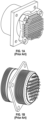
- a connector such as a MIL-DTL-38999 connector (See FIG. 1A and FIG. 1B )
- the pins on the connector are disposed within via holes defined by the PCBA and soldered in place to secure the connector to the PCBA and to connect each of the pins to a component and/or circuit within the PCBA.
- the pins and/or solder joints are typically slightly protruding/raised from the via holes, and if the pins and/or solder joints are located proximate radiating components, they may be susceptible to EMI from those components.
- a frame/heatsink shield would be put in place to shield the radiating components and prevent them from generating EMI in proximately located components.
- this type of shielding may not be achievable due to design constraints, such as the mounting and/or envelope restrictions imposed on the PCBA.
- the size of the sensitive area which needs to be protected from EMI is often quite small as compared to the size of the shielding required for the entire radiating component/circuitry/PCBA.
- An Electromagnetic Interference (EMI) Shielding Assembly (EISA) for a Printed Circuit Board Assembly (PCBA) includes an enclosure, wherein the enclosure defines an enclosure cavity and an electrically conductive foundation associated with PCBA having an area of interest, wherein the electrically conductive foundation at least partially surrounds the area of interest, and wherein the enclosure is securely connected to the PCBA to completely cover the area of interest and to contact the electrically conductive foundation.
- EMI Electromagnetic Interference
- EISA Electromagnetic Interference Shielding Assembly
- PCBA Printed Circuit Board Assembly
- the area of interest is contained within the enclosure cavity.
- the enclosure is constructed from an electromagnetic shielding material.
- the enclosure is constructed from a ferrite material.
- the electrically conductive foundation includes a plurality of mounting surfaces located along a perimeter of the area of interest.
- the electrically conductive foundation further includes at least one conductive metal trace which is located along the perimeter of the area of interest and which conductively connects the plurality of mounting surfaces.
- At least one of the plurality of mounting surfaces is configured to be connected to a ground potential.
- the area of interest is a connector pin field which includes at least one connector pin that protrudes from the PCBA.
- the enclosure cavity includes a cavity height, a cavity width and a cavity length, wherein the cavity height, cavity width and cavity length are sized to completely enclose and contain the connector pin field.
- An Electromagnetic Interference (EMI) Shielding Assembly (EISA) for a PCBA includes an enclosure, wherein the enclosure defines an enclosure cavity and a PCBA, wherein the PCBA includes a connector pin field which includes at least one connector pin and which is external to the PCBA, and an electrically conductive foundation associated with the PCBA to at least partially surround the connector pin field, wherein the enclosure is securely connected to the PCBA to contact the electrically conductive foundation and to completely contain the connector pin field within the enclosure cavity.
- EMI Electromagnetic Interference
- EISA Electromagnetic Interference
- the enclosure is constructed from an electromagnetic shielding material.
- the enclosure is constructed from a ferrite material.
- the electrically conductive foundation includes a plurality of mounting surfaces located along a perimeter of the connector pin field.
- the electrically conductive foundation further includes a plurality of conductive metal traces which are located along the perimeter of the connector pin field and which conductively connect the plurality of mounting surfaces.
- At least one of the plurality of mounting surfaces is configured to be connected to a ground potential.
- the connector pin field includes at least one connector pin that protrudes from the PCBA.
- the enclosure cavity includes a cavity height, a cavity width and a cavity length, wherein the cavity height, cavity width and cavity length are sized to completely enclose and contain the connector pin field.
- a method for shielding an area of interest on a PCBA from EMI includes identifying an area of interest on a PCBA design to be shielded from EMI, wherein the PCBA includes a conductive foundation configurable to a ground potential and surrounding the area of interest, locating a shielding enclosure on the PCBA to completely cover the area of interest and to be in contact with the conductive foundation and securing the shielding enclosure to the PCBA to electromagnetically seal the area of interest within the shielding enclosure.
- the conductive foundation includes conductive mounting interfaces and, securing includes securing the shielding enclosure with at least one mounting device to be in contact with the conductive mounting interfaces.
- the conductive foundation includes an electrically conductive trace which surrounds at least a portion of the area of interest.
- a PCBA EMI shielding assembly 100 having an enclosure 102 and an electrically conductive foundation 104 is shown being implemented with a connector 50 having mounting feet 75 and a PCBA 128 which is associated with the electrically conductive foundation 104, in accordance with an embodiment.
- the enclosure 102 includes a cover 106, a first sidewall 108, a second sidewall 110, a third sidewall 112 and a fourth sidewall 114 which define an enclosure cavity 116.
- the cover 106 includes a cover top surface 118 and a cover bottom surface 120, and each of the first sidewall 108, second sidewall 110, third sidewall 112 and fourth sidewall 114 include a sidewall bottom surface 122 having a sidewall width SW.
- the enclosure cavity 116 includes a cavity height H, a cavity width W and a cavity length L which is sized and shaped to cover and contain an area of interest on the PCBA 128, such as a connector pin field 150.
- the enclosure 102 further defines a plurality of enclosure mounting cavities 124 which are surrounded by enclosure interface surfaces 125 located in each corner of the enclosure 102 and which communicate the cover top surface 118 with the sidewall bottom surface 122. Each of the enclosure mounting cavities 124 are sized and shaped to contain a mounting device 126, such as a mounting screw (See FIG. 2 ).
- the PCBA 128 defines a plurality of PCBA mounting cavities 130 each of which are sized and shaped to contain the mounting device 126.
- the foundation 104 is associated with and/or fabricated into the PCBA 128, in accordance with an embodiment.
- the foundation 104 includes a plurality of mounting interfaces 132 which are constructed from a conductive material and which are configured to be connected to a ground potential.
- each of the plurality of mounting interfaces 132 are associated with a PCBA mounting cavity 130, wherein the mounting interface 132 may or may not surround (wholly or partially) the opening to the PCBA mounting cavity 130.
- the foundation 104' may include one or more foundation (conductive metal) traces 200 which may be associated with and/or fabricated into the PCBA 128' to at least electrically connect and/or partially extend between each of the mounting interfaces 132'. It is contemplated that in other embodiments, the PCBA 128 may be modified to includes a conductive foundation 104 in a retrofit fashion.
- the plurality of mounting interfaces 132 are arranged and located such that they surround a PCBA area of interest, such as connector pin field 150 which is susceptible to EMI.
- the enclosure 102 and the enclosure cavity 120 is sized and shaped such that the enclosure mounting cavities 124 align with the PCBA mounting cavities 130 and such that the connector pin field 150 fits within the enclosure cavity 120. Accordingly, when a connector 50 is securely associated with a PCBA 128 such that the connector pin field 150 is protruding from the PCBA 128, the enclosure 102 is disposed such that the enclosure interface surfaces 125 are aligned with and contacting the mounting interfaces 132.
- Mounting devices 126 are located within each enclosure mounting cavity 124 and the associated PCBA mounting cavity 130.
- the mounting devices 126 are secured to the connector 50 (such as by a nut or screw) to securely associate the enclosure 102, the PCBA 128 and the connector 50 together.
- each of the sidewall bottom surfaces 122 may include a conductive coating and/or the foundation 104 may be constructed from a conductive material (i.e., copper, etc.) that is configured to be conductively connected to a local or system ground potential.
- an operational block diagram illustrating one embodiment of a method 600 for shielding an area of interest on a PCBA, such as a connector pin field 150, is provided and includes identifying an area of interest on a PCBA design to be shielded from EMI, as shown in operational block 602.
- the PCBA 128 is constructed to include a foundation 104 which has a footprint that at least partially surrounds area of interest, as shown in operational block 604.
- the foundation 104 may include a plurality of mounting interfaces 132 which are constructed from a conductive material and which are configured to be connected to a local and/or system ground potential.
- the foundation 104 may also include conductive metal traces 200 that conductively connect the plurality of mounting interfaces 132 together.
- a connector 50 having a plurality of connector pins is securely associated with the PCBA 128 wherein the plurality of connector pins are located and exposed within the connector pin field 150, as shown in operational block 606.
- An enclosure 102 having the same footprint as the foundation 104, is located on the PCBA 128 to cover the connector pin field 150, as shown in operational block 608.
- the enclosure 102 is located on the PCBA 128 such that the connector pin field 150 is located within the enclosure cavity 120 and such that enclosure interface surfaces 125 are aligned with and contact the mounting interfaces 132.
- the enclosure 102 is securely connected to the PCBA 128 via mounting devices 126, as shown in operational block 610.
- the enclosure 102 is securely connected to the PCBA 128 such that the sidewall bottom surfaces 122 and the enclosure interface surfaces 125 are compressingly in contact with the foundation 104 to create a seal between the enclosure 102 and the PCBA 128.
- PCBA EMI shielding assembly 100 provides for a localized shield component to protect board-side connector pins from EMI threats and utilizes existing connector envelopes, mounting features and hardware. Moreover, the PCBA EMI shielding assembly 100 of the invention provides for EMI shielding of the connector pin field while providing physical protection of connector pin field using the existing connector board footprint and mounting provisions. Additionally, the invention allows for the interfacing with existing board grounding surfaces (e.g. wagon wheels, copper moating) and can be made from alternate materials to shield against different EMI field types. Furthermore, the invention eliminates the need for additional shielding features on neighboring components and PCBAs, and requires no additional hardware for installation, utilizes existing connector hardware. Moreover, the present invention provides the ability to retrofit existing designs while allowing for a common, scalable design solution for various connector sizes and shapes.
- existing board grounding surfaces e.g. wagon wheels, copper moating
- PCBA i.e., a PCB containing components
- PCB i.e., an unpopulated printed circuit board
- a newly designed PCB may be designed having mounting interfaces 132, 132', mounting cavities 130, an electrically conductive foundation 104, 104' and/or conductive metal traces 200.
Landscapes
- Engineering & Computer Science (AREA)
- Microelectronics & Electronic Packaging (AREA)
- Shielding Devices Or Components To Electric Or Magnetic Fields (AREA)
Abstract
An Electromagnetic Interference (EMI) Shielding Assembly (EISA) for a PCBA is provided and includes an enclosure (102), wherein the enclosure (102) defines an enclosure cavity and an electrically conductive foundation (104) associated with a PCBA having an area of interest, wherein the electrically conductive foundation (104) at least partially surrounds the area of interest, and wherein the enclosure is securely connected to the PCBA to completely cover the area of interest and to contact the electrically conductive foundation (104).
Description
- The present disclosure relates to an Electromagnetic Interference (EMI) shield, and more particularly to an EMI shield assembly for a Printed Circuit Board Assembly (PCBA).
- Electromagnetic Interference (EMI) is any unwanted noise or interference in an electrical path or circuit caused by an electromagnetic field generated from an outside source. EMI can be caused by natural events, man-made sources and inherent sources. Natural events (e.g., solar flares, lightning storms) can cause EMI to occur in electronic devices due to bombardment of highly charged particles (solar flares) or strong electrostatic discharges and magnetic pulses (lightning storms). Man-made EMI is typically caused by man-made devices, equipment and structures such as communication towers, high-voltage power lines, radar systems and other electronic equipment (such as microwave devices, cell phones, etc.).
- On the other hand, inherent EMI is typically caused by a device's own internal components which can radiate energy that causes interference with other internal components. And as electronics become smaller, faster and the components are more tightly packed together, this problem is exacerbated in that the electronics are more sensitive and more susceptible to the effects of EMI. In the electronics design industry, the threat of EMI to the health of a Printed Circuit Board Assembly (PCBA) and its onboard circuitry can be critical. For more complex electronic assemblies such as critical flight and engine controls, prevention and/or mitigation of EMI effects is especially important due to the critical functional requirements of these designs/components. In fact, failure of a mission critical component can result in the loss of aircraft and/or a life. Unfortunately, however, within these assemblies, design restrictions sometimes do not allow for the full separation or encapsulation of EMI-radiating areas to shield nearby EMI-sensitive circuitry.
- Historically, EMI shielding has been achieved by using covers, tapes and/or frames/heatsinks to encapsulate the radiating component, circuit or PCBA. These design solutions help to keep the radiating areas from affecting nearby EMI-sensitive circuitry. One example of a common EMI shielding approach is used for a PCBA when a connector, such as a MIL-DTL-38999 connector (See
FIG. 1A and FIG. 1B ), is associated with a PCBA. In this case, the pins on the connector are disposed within via holes defined by the PCBA and soldered in place to secure the connector to the PCBA and to connect each of the pins to a component and/or circuit within the PCBA. As shown inFIG. 1C and FIG. 1D , in this type of connection, the pins and/or solder joints are typically slightly protruding/raised from the via holes, and if the pins and/or solder joints are located proximate radiating components, they may be susceptible to EMI from those components. Referring toFIG. 1E , in order to minimize and/or prevent EMI, a frame/heatsink shield would be put in place to shield the radiating components and prevent them from generating EMI in proximately located components. Unfortunately, however, in certain situations, this type of shielding may not be achievable due to design constraints, such as the mounting and/or envelope restrictions imposed on the PCBA. In addition, the size of the sensitive area which needs to be protected from EMI is often quite small as compared to the size of the shielding required for the entire radiating component/circuitry/PCBA. - An Electromagnetic Interference (EMI) Shielding Assembly (EISA) for a Printed Circuit Board Assembly (PCBA) is provided and includes an enclosure, wherein the enclosure defines an enclosure cavity and an electrically conductive foundation associated with PCBA having an area of interest, wherein the electrically conductive foundation at least partially surrounds the area of interest, and wherein the enclosure is securely connected to the PCBA to completely cover the area of interest and to contact the electrically conductive foundation.
- In addition to one or more of the features described above, or as an alternative to any of the foregoing embodiments, the area of interest is contained within the enclosure cavity.
- In addition to one or more of the features described above, or as an alternative to any of the foregoing embodiments, the enclosure is constructed from an electromagnetic shielding material.
- In addition to one or more of the features described above, or as an alternative to any of the foregoing embodiments, the enclosure is constructed from a ferrite material.
- In addition to one or more of the features described above, or as an alternative to any of the foregoing embodiments, the electrically conductive foundation includes a plurality of mounting surfaces located along a perimeter of the area of interest.
- In addition to one or more of the features described above, or as an alternative to any of the foregoing embodiments, the electrically conductive foundation further includes at least one conductive metal trace which is located along the perimeter of the area of interest and which conductively connects the plurality of mounting surfaces.
- In addition to one or more of the features described above, or as an alternative to any of the foregoing embodiments, at least one of the plurality of mounting surfaces is configured to be connected to a ground potential.
- In addition to one or more of the features described above, or as an alternative to any of the foregoing embodiments, the area of interest is a connector pin field which includes at least one connector pin that protrudes from the PCBA.
- In addition to one or more of the features described above, or as an alternative to any of the foregoing embodiments, the enclosure cavity includes a cavity height, a cavity width and a cavity length, wherein the cavity height, cavity width and cavity length are sized to completely enclose and contain the connector pin field.
- An Electromagnetic Interference (EMI) Shielding Assembly (EISA) for a PCBA is provided and includes an enclosure, wherein the enclosure defines an enclosure cavity and a PCBA, wherein the PCBA includes a connector pin field which includes at least one connector pin and which is external to the PCBA, and an electrically conductive foundation associated with the PCBA to at least partially surround the connector pin field, wherein the enclosure is securely connected to the PCBA to contact the electrically conductive foundation and to completely contain the connector pin field within the enclosure cavity.
- In addition to one or more of the features described above, or as an alternative to any of the foregoing embodiments, the enclosure is constructed from an electromagnetic shielding material.
- In addition to one or more of the features described above, or as an alternative to any of the foregoing embodiments, the enclosure is constructed from a ferrite material.
- In addition to one or more of the features described above, or as an alternative to any of the foregoing embodiments, the electrically conductive foundation includes a plurality of mounting surfaces located along a perimeter of the connector pin field.
- In addition to one or more of the features described above, or as an alternative to any of the foregoing embodiments, the electrically conductive foundation further includes a plurality of conductive metal traces which are located along the perimeter of the connector pin field and which conductively connect the plurality of mounting surfaces.
- In addition to one or more of the features described above, or as an alternative to any of the foregoing embodiments, at least one of the plurality of mounting surfaces is configured to be connected to a ground potential.
- In addition to one or more of the features described above, or as an alternative to any of the foregoing embodiments, the connector pin field includes at least one connector pin that protrudes from the PCBA.
- In addition to one or more of the features described above, or as an alternative to any of the foregoing embodiments, the enclosure cavity includes a cavity height, a cavity width and a cavity length, wherein the cavity height, cavity width and cavity length are sized to completely enclose and contain the connector pin field.
- A method for shielding an area of interest on a PCBA from EMI, wherein the method includes identifying an area of interest on a PCBA design to be shielded from EMI, wherein the PCBA includes a conductive foundation configurable to a ground potential and surrounding the area of interest, locating a shielding enclosure on the PCBA to completely cover the area of interest and to be in contact with the conductive foundation and securing the shielding enclosure to the PCBA to electromagnetically seal the area of interest within the shielding enclosure.
- In addition to one or more of the features described above, or as an alternative to any of the foregoing embodiments, the conductive foundation includes conductive mounting interfaces and, securing includes securing the shielding enclosure with at least one mounting device to be in contact with the conductive mounting interfaces.
- In addition to one or more of the features described above, or as an alternative to any of the foregoing embodiments, the conductive foundation includes an electrically conductive trace which surrounds at least a portion of the area of interest.
- The following descriptions should not be considered limiting in any way. With reference to the accompanying drawings, like elements are numbered alike:
-
FIG. 1A is a perspective view of a custom connector with mounting feet, in accordance with the prior art; -
FIG. 1B is a perspective view of a standard connector without mounting feet, in accordance with the prior art; -
FIG. 1C is a top down, side view of the connector ofFIG. 1A mounted to a Printed Circuit Board (PCB) showing the exposed connector pin field, in accordance with the prior art; -
FIG. 1D is a side view of the connector ofFIG. 1A mounted to a PCB showing the exposed connector pin field, in accordance with the prior art; -
FIG. 1E is a side view of the connector/combination ofFIG. 1D and a second PCBA having shielded radiating components located proximate the exposed connector pin field, in accordance with the prior art; -
FIG. 2 is a side sectional view of a connector with mounting feet connected to a PCBA implementing the PCBA EMI shielding assembly, in accordance with an embodiment of the invention; -
FIG. 3A is a bottom perspective view of an enclosure of the PCBA EMI shielding assembly ofFIG. 2 , in accordance with an embodiment of the invention; -
FIG. 3B is a top perspective view of an enclosure of the PCBA EMI shielding assembly ofFIG. 2 , in accordance with an embodiment of the invention; -
FIG. 4A is a top view of a foundation of the PCBA EMI shielding assembly ofFIG. 2 associated with a PCBA, in accordance with an embodiment of the invention; -
FIG. 4B is a top view of a foundation of the PCBA EMI shielding assembly ofFIG. 2 associated with a PCBA, in accordance with another embodiment of the invention; -
FIG. 5A is a top perspective view of a connector with mounting feet connected to a PCBA implementing the PCBA EMI shielding assembly, in accordance with an embodiment of the invention; -
FIG. 5B is a top transparent view of a connector with mounting feet connected to a PCBA implementing the PCBA EMI shielding assembly, in accordance with an embodiment of the invention; -
FIG. 6A is a side perspective sectional view of a connector with mounting feet connected to a PCBA implementing the PCBA EMI shielding assembly, in accordance with an embodiment of the invention; -
FIG. 6B is a side view of a connector with mounting feet connected to a PCBA implementing the PCBA EMI shielding assembly, in accordance with an embodiment of the invention; and -
FIG. 7 is an operational block diagram illustrating a method of implementing a PCBA EMI shielding assembly to shield an area of interest on a circuit board, in accordance with an embodiment of the invention. - A detailed description of one or more embodiments of the disclosed apparatus and method are presented herein by way of exemplification and not limitation with reference to the several Figures.
- Referring to
FIG. 2 , a PCBAEMI shielding assembly 100 having anenclosure 102 and an electricallyconductive foundation 104 is shown being implemented with aconnector 50 having mountingfeet 75 and aPCBA 128 which is associated with the electricallyconductive foundation 104, in accordance with an embodiment. Referring toFIG. 3A and FIG. 3B , theenclosure 102 includes acover 106, afirst sidewall 108, asecond sidewall 110, athird sidewall 112 and afourth sidewall 114 which define anenclosure cavity 116. Thecover 106 includes a covertop surface 118 and a coverbottom surface 120, and each of thefirst sidewall 108,second sidewall 110,third sidewall 112 andfourth sidewall 114 include asidewall bottom surface 122 having a sidewall width SW. Theenclosure cavity 116 includes a cavity height H, a cavity width W and a cavity length L which is sized and shaped to cover and contain an area of interest on thePCBA 128, such as aconnector pin field 150. Theenclosure 102 further defines a plurality ofenclosure mounting cavities 124 which are surrounded by enclosure interface surfaces 125 located in each corner of theenclosure 102 and which communicate the covertop surface 118 with thesidewall bottom surface 122. Each of theenclosure mounting cavities 124 are sized and shaped to contain a mountingdevice 126, such as a mounting screw (SeeFIG. 2 ). - In accordance with an embodiment and referring to
FIG. 4A , thePCBA 128 defines a plurality ofPCBA mounting cavities 130 each of which are sized and shaped to contain the mountingdevice 126. Thefoundation 104 is associated with and/or fabricated into thePCBA 128, in accordance with an embodiment. Thefoundation 104 includes a plurality of mountinginterfaces 132 which are constructed from a conductive material and which are configured to be connected to a ground potential. Moreover, each of the plurality of mountinginterfaces 132 are associated with aPCBA mounting cavity 130, wherein the mountinginterface 132 may or may not surround (wholly or partially) the opening to thePCBA mounting cavity 130. Referring toFIG. 4B , it should be appreciated that in another embodiment, the foundation 104' may include one or more foundation (conductive metal) traces 200 which may be associated with and/or fabricated into the PCBA 128' to at least electrically connect and/or partially extend between each of the mounting interfaces 132'. It is contemplated that in other embodiments, thePCBA 128 may be modified to includes aconductive foundation 104 in a retrofit fashion. - Referring to
FIG. 5A, FIG. 5B ,FIG. 6A, FIG. 6B and again toFIG. 4A , the plurality of mountinginterfaces 132 are arranged and located such that they surround a PCBA area of interest, such asconnector pin field 150 which is susceptible to EMI. Moreover, theenclosure 102 and theenclosure cavity 120 is sized and shaped such that theenclosure mounting cavities 124 align with thePCBA mounting cavities 130 and such that theconnector pin field 150 fits within theenclosure cavity 120. Accordingly, when aconnector 50 is securely associated with aPCBA 128 such that theconnector pin field 150 is protruding from thePCBA 128, theenclosure 102 is disposed such that the enclosure interface surfaces 125 are aligned with and contacting the mounting interfaces 132. Mountingdevices 126 are located within eachenclosure mounting cavity 124 and the associatedPCBA mounting cavity 130. The mountingdevices 126 are secured to the connector 50 (such as by a nut or screw) to securely associate theenclosure 102, thePCBA 128 and theconnector 50 together. - It should be appreciated that in an embodiment the
enclosure 102 may be constructed from a ferrite material which acts to shield theconnector pin field 150 from EMI. Additionally, each of the sidewall bottom surfaces 122 may include a conductive coating and/or thefoundation 104 may be constructed from a conductive material (i.e., copper, etc.) that is configured to be conductively connected to a local or system ground potential. - Referring to
FIG. 7 , an operational block diagram illustrating one embodiment of amethod 600 for shielding an area of interest on a PCBA, such as aconnector pin field 150, is provided and includes identifying an area of interest on a PCBA design to be shielded from EMI, as shown inoperational block 602. ThePCBA 128 is constructed to include afoundation 104 which has a footprint that at least partially surrounds area of interest, as shown inoperational block 604. As discussed hereinabove, thefoundation 104 may include a plurality of mountinginterfaces 132 which are constructed from a conductive material and which are configured to be connected to a local and/or system ground potential. In another embodiment, thefoundation 104 may also include conductive metal traces 200 that conductively connect the plurality of mountinginterfaces 132 together. Aconnector 50 having a plurality of connector pins is securely associated with thePCBA 128 wherein the plurality of connector pins are located and exposed within theconnector pin field 150, as shown inoperational block 606. - An
enclosure 102, having the same footprint as thefoundation 104, is located on thePCBA 128 to cover theconnector pin field 150, as shown inoperational block 608. Theenclosure 102 is located on thePCBA 128 such that theconnector pin field 150 is located within theenclosure cavity 120 and such that enclosure interface surfaces 125 are aligned with and contact the mounting interfaces 132. Theenclosure 102 is securely connected to thePCBA 128 via mountingdevices 126, as shown inoperational block 610. Theenclosure 102 is securely connected to thePCBA 128 such that the sidewall bottom surfaces 122 and the enclosure interface surfaces 125 are compressingly in contact with thefoundation 104 to create a seal between theenclosure 102 and thePCBA 128. - It should be appreciated that PCBA
EMI shielding assembly 100 provides for a localized shield component to protect board-side connector pins from EMI threats and utilizes existing connector envelopes, mounting features and hardware. Moreover, the PCBAEMI shielding assembly 100 of the invention provides for EMI shielding of the connector pin field while providing physical protection of connector pin field using the existing connector board footprint and mounting provisions. Additionally, the invention allows for the interfacing with existing board grounding surfaces (e.g. wagon wheels, copper moating) and can be made from alternate materials to shield against different EMI field types. Furthermore, the invention eliminates the need for additional shielding features on neighboring components and PCBAs, and requires no additional hardware for installation, utilizes existing connector hardware. Moreover, the present invention provides the ability to retrofit existing designs while allowing for a common, scalable design solution for various connector sizes and shapes. - The term "about" is intended to include the degree of error associated with measurement of the particular quantity based upon the equipment available at the time of filing the application. It should be appreciated that although the invention is disclosed herein with regards to a PCBA (i.e., a PCB containing components), the invention is also applicable to a PCB (i.e., an unpopulated printed circuit board) being prepared for population with components. For example, a newly designed PCB may be designed having mounting
interfaces 132, 132', mountingcavities 130, an electricallyconductive foundation 104, 104' and/or conductive metal traces 200. - The terminology used herein is for the purpose of describing particular embodiments only and is not intended to be limiting of the present disclosure. As used herein, the singular forms "a", "an" and "the" are intended to include the plural forms as well, unless the context clearly indicates otherwise. It will be further understood that the terms "comprises" and/or "comprising," when used in this specification, specify the presence of stated features, integers, steps, operations, elements, and/or components, but do not preclude the presence or addition of one or more other features, integers, steps, operations, element components, and/or groups thereof.
- While the present disclosure has been described with reference to an exemplary embodiment or embodiments, it will be understood by those skilled in the art that various changes may be made and equivalents may be substituted for elements thereof without departing from the scope of the present disclosure. Moreover, the embodiments or parts of the embodiments may be combined in whole or in part without departing from the scope of the invention. In addition, many modifications may be made to adapt a particular situation or material to the teachings of the present disclosure without departing from the essential scope thereof. Therefore, it is intended that the present disclosure not be limited to the particular embodiment disclosed as the best mode contemplated for carrying out this disclosure, but that the present disclosure will include all embodiments falling within the scope of the claims.
Claims (15)
- An Electromagnetic Interference "EMI" Shielding Assembly "EISA" for a Printed Circuit Board Assembly "PCBA", comprising:an enclosure (102), wherein the enclosure (102) defines an enclosure cavity; andan electrically conductive foundation (104) associated with a PCBA having an area of interest,wherein the electrically conductive foundation (104) at least partially surrounds the area of interest, andwherein the enclosure (102) is securely connected to the PCBA to completely cover the area of interest and to contact the electrically conductive foundation (104).
- The EISA of claim 1, wherein the area of interest is contained within the enclosure cavity.
- The EISA of claim 1 or 2, wherein the enclosure (102) is constructed from an electromagnetic shielding material, or wherein the enclosure (102) is constructed from a ferrite material.
- The EISA of any preceding claim, wherein the electrically conductive foundation (104) includes a plurality of mounting surfaces located along a perimeter of the area of interest.
- The EISA of claim 4, wherein the electrically conductive foundation (104) further includes at least one conductive metal trace which is located along the perimeter of the area of interest and which conductively connects the plurality of mounting surfaces, or wherein at least one of the plurality of mounting surfaces is configured to be connected to a ground potential.
- The EISA of any preceding claim, wherein the area of interest is a connector pin field which includes at least one connector pin that protrudes from the PCBA.
- The EISA of any preceding claim,wherein the enclosure cavity includes a cavity height, a cavity width and a cavity length, andwherein the cavity height, cavity width and cavity length are sized to completely enclose and contain the connector pin field.
- An Electromagnetic Interference "EMI" Shielding Assembly "EISA" for a Printed Circuit Board Assembly "PCBA", comprising:an enclosure (102), wherein the enclosure (102) defines an enclosure cavity; anda PCBA, wherein the PCBA includesa connector pin field which includes at least one connector pin and which is external to the PCBA, andan electrically conductive foundation (104) associated with the PCBA to at least partially surround the connector pin field,wherein the enclosure (102) is securely connected to the PCBA to contact the electrically conductive foundation (104) and to completely contain the connector pin field within the enclosure cavity.
- The EISA of claim 8, wherein the enclosure (102) is constructed from an electromagnetic shielding material, or wherein the enclosure (102) is constructed from a ferrite material.
- The EISA of claim 8, wherein the electrically conductive foundation (104) includes a plurality of mounting surfaces located along a perimeter of the connector pin field.
- The EISA of claim 10, wherein the electrically conductive foundation (104) further includes a plurality of conductive metal traces which are located along the perimeter of the connector pin field and which conductively connect the plurality of mounting surfaces.
- The EISA of claim 10, wherein at least one of the plurality of mounting surfaces is configured to be connected to a ground potential, or wherein the connector pin field includes at least one connector pin that protrudes from the PCBA.
- The EISA of claim 8,wherein the enclosure cavity includes a cavity height, a cavity width and a cavity length, andwherein the cavity height, cavity width and cavity length are sized to completely enclose and contain the connector pin field.
- A method for shielding an area of interest on a Printed Circuit Board Assembly "PCBA" from EMI, the method comprising:identifying an area of interest on a PCBA design to be shielded from EMI, wherein the PCBA includes a conductive foundation (104) configurable to a ground potential and surrounding the area of interest;locating a shielding enclosure (102) on the PCBA to completely cover the area of interest and to be in contact with the conductive foundation (104); andsecuring the shielding enclosure (102) to the PCBA to electromagnetically seal the area of interest within the shielding enclosure (102).
- The method of claim 14,wherein the conductive foundation (104) includes conductive mounting interfaces and,wherein securing includes securing the shielding enclosure (102) with at least one mounting device to be in contact with the conductive mounting interfaces, and optionally wherein the conductive foundation (104) includes an electrically conductive trace which surrounds at least a portion of the area of interest.
Applications Claiming Priority (1)
| Application Number | Priority Date | Filing Date | Title |
|---|---|---|---|
| US18/342,432 US20250007221A1 (en) | 2023-06-27 | 2023-06-27 | Integrated scalable connector pin field emi shielding assembly and a method for implementing same |
Publications (1)
| Publication Number | Publication Date |
|---|---|
| EP4486085A1 true EP4486085A1 (en) | 2025-01-01 |
Family
ID=91581910
Family Applications (1)
| Application Number | Title | Priority Date | Filing Date |
|---|---|---|---|
| EP24182536.3A Pending EP4486085A1 (en) | 2023-06-27 | 2024-06-17 | Integrated scalable connector pin field emi shielding assembly and a method for implementing same |
Country Status (2)
| Country | Link |
|---|---|
| US (1) | US20250007221A1 (en) |
| EP (1) | EP4486085A1 (en) |
Citations (4)
| Publication number | Priority date | Publication date | Assignee | Title |
|---|---|---|---|---|
| US5639989A (en) * | 1994-04-19 | 1997-06-17 | Motorola Inc. | Shielded electronic component assembly and method for making the same |
| US5792994A (en) * | 1995-08-09 | 1998-08-11 | Mitsubishi Denki Kabushiki Kaisha | Device for mounting a component |
| EP1033787A1 (en) * | 1999-03-04 | 2000-09-06 | Molex Incorporated | Electrical connector with terminal pins |
| CN108711697A (en) * | 2014-04-09 | 2018-10-26 | 富士康(昆山)电脑接插件有限公司 | Socket connector |
Family Cites Families (10)
| Publication number | Priority date | Publication date | Assignee | Title |
|---|---|---|---|---|
| US5823826A (en) * | 1995-10-30 | 1998-10-20 | The Whitaker Corporation | Filtered circuit connector with frame |
| US6206728B1 (en) * | 1999-02-22 | 2001-03-27 | Molex Incorporated | Shielded electrical connector system |
| US6551134B1 (en) * | 2001-06-11 | 2003-04-22 | Picolight Incorporated | Mounted transceivers |
| US6999323B1 (en) * | 2002-10-17 | 2006-02-14 | Finisar Corporation | Electromagnetic interference containment transceiver module |
| US8393918B2 (en) * | 2008-06-11 | 2013-03-12 | Pulse Electronics, Inc. | Miniaturized connectors and methods |
| US8294043B2 (en) * | 2010-12-07 | 2012-10-23 | Honeywell International Inc. | Integrated connector shield ring for shielded enclosures |
| US9437949B2 (en) * | 2014-09-26 | 2016-09-06 | Tyco Electronics Corporation | Electrical cable assembly configured to be mounted onto an array of electrical contacts |
| US10490949B2 (en) * | 2017-03-15 | 2019-11-26 | Pulse Electronics, Inc. | Integrated connector apparatus for PCIe applications |
| US10686282B1 (en) * | 2019-02-27 | 2020-06-16 | Te Connectivity Corporation | Electrical connector for mitigating electrical resonance |
| US11363746B2 (en) * | 2019-09-06 | 2022-06-14 | Teradyne, Inc. | EMI shielding for a signal trace |
-
2023
- 2023-06-27 US US18/342,432 patent/US20250007221A1/en active Pending
-
2024
- 2024-06-17 EP EP24182536.3A patent/EP4486085A1/en active Pending
Patent Citations (4)
| Publication number | Priority date | Publication date | Assignee | Title |
|---|---|---|---|---|
| US5639989A (en) * | 1994-04-19 | 1997-06-17 | Motorola Inc. | Shielded electronic component assembly and method for making the same |
| US5792994A (en) * | 1995-08-09 | 1998-08-11 | Mitsubishi Denki Kabushiki Kaisha | Device for mounting a component |
| EP1033787A1 (en) * | 1999-03-04 | 2000-09-06 | Molex Incorporated | Electrical connector with terminal pins |
| CN108711697A (en) * | 2014-04-09 | 2018-10-26 | 富士康(昆山)电脑接插件有限公司 | Socket connector |
Also Published As
| Publication number | Publication date |
|---|---|
| US20250007221A1 (en) | 2025-01-02 |
Similar Documents
| Publication | Publication Date | Title |
|---|---|---|
| US4829432A (en) | Apparatus for shielding an electrical circuit from electromagnetic interference | |
| US5586011A (en) | Side plated electromagnetic interference shield strip for a printed circuit board | |
| US4954929A (en) | Multi-layer circuit board that suppresses radio frequency interference from high frequency signals | |
| US5315069A (en) | Electromagnetic radiation reduction technique using grounded conductive traces circumscribing internal planes of printed circuit boards | |
| US10319685B2 (en) | EMI shielded integrated circuit packages and methods of making the same | |
| US5268810A (en) | Electrical connector incorporating EMI filter | |
| US5335147A (en) | EMI shield apparatus and methods | |
| EP0684645A2 (en) | EMF shielding of an integrated circuit package | |
| US5190479A (en) | Electrical connector incorporating EMI/RFI/EMP isolation | |
| US20030218873A1 (en) | Structure for fastening a component | |
| US5304964A (en) | Electrical connector incorporating ground shield spacer | |
| US6839214B2 (en) | Overvoltage protection device | |
| US6944025B2 (en) | EMI shielding apparatus | |
| EP0834964A1 (en) | Shielded electrical receptacle connector assembly | |
| CN104137245A (en) | Low profile, space efficient circuit shields | |
| CN107396621B (en) | Electromagnetic shield for electronic device | |
| US20050276027A1 (en) | Electronic device for shielding EMI | |
| US20040012939A1 (en) | EMI shielding apparatus | |
| US5635775A (en) | Printed circuit board mount electro-magnetic interference suppressor | |
| US20250007221A1 (en) | Integrated scalable connector pin field emi shielding assembly and a method for implementing same | |
| US6707675B1 (en) | EMI containment device and method | |
| CA2240751A1 (en) | Electrical circuit configuration arranged in a casing | |
| US4268105A (en) | Transient suppression connector | |
| US12513875B2 (en) | Electronic control device with resin case | |
| JP5320801B2 (en) | Electronic device and noise shielding method thereof |
Legal Events
| Date | Code | Title | Description |
|---|---|---|---|
| PUAI | Public reference made under article 153(3) epc to a published international application that has entered the european phase |
Free format text: ORIGINAL CODE: 0009012 |
|
| STAA | Information on the status of an ep patent application or granted ep patent |
Free format text: STATUS: THE APPLICATION HAS BEEN PUBLISHED |
|
| AK | Designated contracting states |
Kind code of ref document: A1 Designated state(s): AL AT BE BG CH CY CZ DE DK EE ES FI FR GB GR HR HU IE IS IT LI LT LU LV MC ME MK MT NL NO PL PT RO RS SE SI SK SM TR |
|
| STAA | Information on the status of an ep patent application or granted ep patent |
Free format text: STATUS: REQUEST FOR EXAMINATION WAS MADE |
|
| 17P | Request for examination filed |
Effective date: 20250630 |