EP4485788A1 - Droop control method for parallel inverters - Google Patents
Droop control method for parallel inverters Download PDFInfo
- Publication number
- EP4485788A1 EP4485788A1 EP24184319.2A EP24184319A EP4485788A1 EP 4485788 A1 EP4485788 A1 EP 4485788A1 EP 24184319 A EP24184319 A EP 24184319A EP 4485788 A1 EP4485788 A1 EP 4485788A1
- Authority
- EP
- European Patent Office
- Prior art keywords
- error value
- voltage
- value
- output
- control method
- Prior art date
- Legal status (The legal status is an assumption and is not a legal conclusion. Google has not performed a legal analysis and makes no representation as to the accuracy of the status listed.)
- Pending
Links
Images



Classifications
-
- H—ELECTRICITY
- H02—GENERATION; CONVERSION OR DISTRIBUTION OF ELECTRIC POWER
- H02M—APPARATUS FOR CONVERSION BETWEEN AC AND AC, BETWEEN AC AND DC, OR BETWEEN DC AND DC, AND FOR USE WITH MAINS OR SIMILAR POWER SUPPLY SYSTEMS; CONVERSION OF DC OR AC INPUT POWER INTO SURGE OUTPUT POWER; CONTROL OR REGULATION THEREOF
- H02M1/00—Details of apparatus for conversion
- H02M1/0003—Details of control, feedback or regulation circuits
- H02M1/0025—Arrangements for modifying reference values, feedback values or error values in the control loop of a converter
-
- H—ELECTRICITY
- H02—GENERATION; CONVERSION OR DISTRIBUTION OF ELECTRIC POWER
- H02M—APPARATUS FOR CONVERSION BETWEEN AC AND AC, BETWEEN AC AND DC, OR BETWEEN DC AND DC, AND FOR USE WITH MAINS OR SIMILAR POWER SUPPLY SYSTEMS; CONVERSION OF DC OR AC INPUT POWER INTO SURGE OUTPUT POWER; CONTROL OR REGULATION THEREOF
- H02M7/00—Conversion of AC power input into DC power output; Conversion of DC power input into AC power output
- H02M7/42—Conversion of DC power input into AC power output without possibility of reversal
- H02M7/44—Conversion of DC power input into AC power output without possibility of reversal by static converters
- H02M7/48—Conversion of DC power input into AC power output without possibility of reversal by static converters using discharge tubes with control electrode or semiconductor devices with control electrode
- H02M7/493—Conversion of DC power input into AC power output without possibility of reversal by static converters using discharge tubes with control electrode or semiconductor devices with control electrode the static converters being arranged for operation in parallel
-
- H—ELECTRICITY
- H02—GENERATION; CONVERSION OR DISTRIBUTION OF ELECTRIC POWER
- H02J—ELECTRIC POWER NETWORKS; CIRCUIT ARRANGEMENTS OR SYSTEMS FOR SUPPLYING OR DISTRIBUTING ELECTRIC POWER; SYSTEMS FOR STORING ELECTRIC ENERGY
- H02J3/00—Circuit arrangements for AC mains or AC distribution networks
- H02J3/38—Arrangements for feeding a single network from two or more generators or sources in parallel; Arrangements for feeding already energised networks from additional generators or sources in parallel
-
- H—ELECTRICITY
- H02—GENERATION; CONVERSION OR DISTRIBUTION OF ELECTRIC POWER
- H02J—ELECTRIC POWER NETWORKS; CIRCUIT ARRANGEMENTS OR SYSTEMS FOR SUPPLYING OR DISTRIBUTING ELECTRIC POWER; SYSTEMS FOR STORING ELECTRIC ENERGY
- H02J3/00—Circuit arrangements for AC mains or AC distribution networks
- H02J3/38—Arrangements for feeding a single network from two or more generators or sources in parallel; Arrangements for feeding already energised networks from additional generators or sources in parallel
- H02J3/46—Controlling the sharing of generated power between the generators, sources or networks
- H02J3/48—Controlling the sharing of active power
Definitions
- the present disclosure relates to the field of control, and in particular, to a droop control system and control method for parallel inverters.
- the parallel inverter technology aims to improve the power supply capacity and reliability of a system, and is mainly applied in the fields of static inverter (SIV), uninterruptible power supply (UPS), and distributed generation (DG).
- the parallel inverter technology includes a droop control method, which achieves parallel connection by detecting the output state of each inverter, does not rely on communication signals between inverters, and has high system reliability and wide application.
- the conventional droop control method adopts proportional droop control, which has an inherent contradiction between voltage steady-state error and steady-state power allocation error and a slow response speed. Therefore, a droop control method is needed to reduce voltage steady-state error and steady-state power allocation error, and to improve the response speed of droop control.
- the present disclosure provides a droop control method for parallel inverters, including, for each inverter:
- the droop control method further includes: obtaining the RMS voltage error value based on an RMS voltage reference value and an RMS of an output voltage from the corresponding inverter.
- the droop control method further includes: obtaining the power error value based on an average power of all the parallel inverters and the output power of the corresponding inverter.
- the step of the proportional integral control includes:
- the droop control method further includes: multiplying the output power of the corresponding inverter by a droop coefficient to obtain the droop value of the output power of the corresponding inverter.
- the droop control method further includes: multiplying the RMS voltage target value by a unit sine function with an amplitude of 2 to obtain the alternating current voltage reference value.
- the droop control method further includes: detecting the output voltage of the corresponding inverter through an RMS detector to obtain the RMS of the output voltage.
- the step of obtaining, based on the alternating current voltage reference value, a duty cycle for controlling an output of the corresponding inverter further includes:
- the present disclosure further provides a computer-readable storage medium, including a computer program that can be executed by a processor to implement the steps of the foregoing droop control method for parallel inverters.
- the present disclosure further provides an electronic device, including:
- the droop control system and control method in the present disclosure introduce an average active power loop to eliminate steady-state power allocation errors.
- the droop control does not use an RMS loop, which improves the response speed of droop control.
- FIG. 1 illustrates an equivalent circuit of parallel inverters.
- Two inverters, inv1 and inv2 are connected in parallel to jointly supply power to load 103.
- Inverter inv1 is equivalent to power supply 101 and impedor Z1, the voltage of power supply 101 is V 1 ⁇ 1, and the output current of inverter inv1 is I 1 .
- Inverter inv2 is equivalent to power supply 102 and impedor Z2, the voltage of inverter inv2 is V 2 ⁇ 2, and the output current of inverter inv2 is I 2 .
- Inverter inv1 and inverter inv2 are connected in parallel to load 103 to jointly supply power to load 103, and the input voltage of load 103 is V 0 ⁇ 0.
- v i represents an amplitude of an equivalent power supply voltage of the i th inverter
- ⁇ i represents a phase of the equivalent power supply voltage of the i th inverter
- Z i represents an equivalent impedance of the i th inverter
- K V_P represents a voltage power proportion coefficient
- V refi V noi ⁇ K V _ droop ⁇ P oi
- V refi represents a reference voltage for droop control
- V noi represents an initial voltage for droop control
- K V_droop represents a droop coefficient, which is a fixed value.
- the droop coefficient may alternatively be adjusted for small-scale testing.
- V ref 1 V no 1 ⁇ K V _ droop ⁇ P o 1
- V ref2 V no2 ⁇ K V _ droop ⁇ P o2
- the initial voltages of inverter inv1 and inverter inv2 for droop control are the same, both of which are 220V.
- the equivalent power supply voltage V1 of inverter inv1 is equal to its reference voltage V ref1
- the equivalent power supply voltage V2 of inverter inv2 is equal to its reference voltage V ref2 .
- a control system in a discrete domain (z domain) shown in FIG. 2 can be obtained, where z is a change operator.
- the control system includes a subtractor 201, a multiplier 202, an adder 203, and a multiplier 204.
- the subtractor 201 is configured to receive a power difference reference value 0 and an output power difference ⁇ P ( z ) of two inverters and subtract one from another to obtain an error value - ⁇ P ( z ).
- the multiplier 202 is configured to multiply the error value by a droop coefficient K V_droop for output.
- the adder is configured to receive the output from the multiplier 202 and a difference ⁇ V n ( z ) between initial voltages of two UPS and add the two to obtain a difference ⁇ V out ( z ) between reference voltages of the two inverters.
- ⁇ V out ( z ) is equal to ⁇ V ( z ).
- the multiplier 204 is configured to multiply the difference ⁇ V out (z) between the reference voltages of the two UPS by a reciprocal K V_P -1 of a voltage power proportion coefficient K V_P and output the output power difference ⁇ P ( z ) of the two inverters.
- the steady-state power allocation error is the difference between the output power of the two inverters, namely, ⁇ P ( z ).
- the steady-state power allocation error is a difference between output power of the current inverter and average output power of the N parallel inverters. From Equation (6), it can be seen that the larger the droop coefficient, the smaller the steady-state power allocation error.
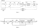
- FIG. 3 illustrates a schematic diagram of a droop control system for parallel inverters in an existing technology.
- the droop control system includes a root mean square (RMS) loop, power droop control, and a voltage and current loop controller 308.
- the power droop control includes a multiplier 302.
- the RMS loop includes a subtractor 301, a subtractor 303, a multiplier 304, and an integrator 305.
- the multiplier 302 is configured to receive output power (active power) from an inverter (controlled object) 309, multiply the output power by a droop coefficient K V_droop , and output a droop value.
- the subtractor 301 is configured to receive an RMS voltage reference value Vrms.ref and the droop value from the multiplier 302 and subtract one from another for output.
- An RMS detector 306 is configured to receive an output voltage Vout from the inverter 309, detect an RMS of the output voltage Vout, and output a voltage feedback value Vrms.fb.
- the subtractor 303 is configured to receive the output from the subtractor 301 and the voltage feedback value Vrms.fb from the RMS detector 306 and subtract one from another to output a voltage error value e.
- the multiplier 304 is configured to receive the voltage error value e from the subtractor 303 and multiply the same by an integration coefficient Ki for output.
- the integrator 305 is configured to receive the output from the multiplier 304, integrate the output, and then output an RMS target value Vrms.tgt.
- the multiplier 307 is configured to receive the RMS target value Vrms.tgt from the integrator 305, multiply the Vrms.tgt by a unit sine function sin with an amplitude of 2 , and output an alternating current voltage reference value Vac.ref.
- FIG. 4 illustrates a schematic diagram of a voltage and current loop controller according to an embodiment of the present disclosure. It should be understood that the voltage and current loop controller in FIG. 4 is only an example and does not constitute a limitation to the present disclosure.
- the voltage and current loop controller includes a subtractor 401, a proportional integral controller 402, a subtractor 403, and a proportional integral controller 404.
- the subtractor 401 is configured to receive the alternating current voltage reference value Vac.ref from the droop control system shown in FIG. 3 and an output voltage Vout from an inverter 405, and subtract one from another to output an alternating current voltage error value.
- the proportional integral controller 402 is configured to receive the alternating current voltage error value from the subtractor 401, perform proportional integral control on the alternating current voltage error value, and then output a current reference value Iref.
- the subtractor 403 is configured to receive the current reference value Iref from the proportional integral controller 402 and output current IL from the inverter 405, and subtract one from another to output a current error value.
- the proportional integral controller 404 is configured to receive the current error value from the subtractor 403, perform proportional integral control on the current error value, and then output a duty cycle d.
- the duty cycle d is input into the inverter 405 to control the output voltage Vout and output current IL of the inverter 405.
- the droop control method in the above embodiment adds the droop value calculated by multiplying the output active power P of the inverter by the droop coefficient K V_droop to the RMS voltage reference value Vrms.ref of the inverter RMS loop.
- the obvious defect of this method is steady-state error, and because droop control also uses the RMS loop, the response speed of droop control is affected.
- the steady-state error is a difference between the output voltage of the inverter and the alternating current voltage reference value Vac.ref (namely, target voltage) in a steady state.
- the larger the droop coefficient the larger the steady-state error, but the larger the droop coefficient, the smaller the steady-state power allocation error.
- the foregoing droop control method is proportional control, so the steady-state power allocation error cannot be eliminated.
- FIG. 5 illustrates a schematic diagram of a droop control system for parallel inverters according to an embodiment of the present disclosure.
- the droop control system is used for controlling output power of a current inverter, so that all parallel inverters have nearly the same output power.
- the droop control system includes an RMS loop, an average power loop, power droop control, and a voltage and current loop controller 511.
- the average power loop includes a subtractor 505 and a multiplier 506.
- the subtractor 505 is configured to receive average active power P of all parallel inverters and an output active power Po of the current inverter and subtract one from another to output a power error value.
- the multiplier 506 is configured to receive the power error value from the subtracter 505, multiply the power error value by a power proportion coefficient Ki_p, and output a gain of the power error value.
- the multiplier 506 may alternatively be omitted, and in this case, the power proportion coefficient Ki_p is 1.
- the RMS loop includes an RMS detector 509, a subtractor 501, a multiplier 502, an adder 503, and an integrator 504.
- the RMS detector 509 is configured to receive an output voltage Vout from an inverter 512, detect an RMS of the voltage, and output an RMS voltage feedback value Vrms.fb.
- the subtractor 501 is configured to receive an RMS voltage reference value Vrms.ref and the RMS voltage feedback value Vrms.fb from the RMS detector 509, and subtract one from another to output an RMS voltage error value.
- the multiplier 502 is configured to receive the RMS voltage error value from the subtractor 501, multiply the RMS voltage error value by a voltage proportion coefficient Ki_v, and output a gain of the RMS voltage error value.
- the multiplier 502 may alternatively be omitted, and in this case, the voltage proportion coefficient Ki_v is 1.
- the adder 503 is configured to receive the gain of the RMS voltage error value from the multiplier 502 and the gain of the power error value from the multiplier 506, and add the gains to output a sum error value.
- the integrator 504 is configured to receive the output from the adder 503, integrate the output, and output an integral error value.
- the RMS can be directly calculated by the output voltage Vout of the inverter, that is, the RMS detector 509 can be omitted.
- the power droop control includes: a multiplier 508, configured to receive an output power (active power) from the inverter, multiply the output power by a droop coefficient K V_droop , and output a power droop value.
- a subtractor 507 configured to receive the integral error value from the integrator 504 and the power droop value from the multiplier 508, and subtract one from another to output an RMS voltage target value Vrms.tgt.
- a multiplier 510 configured to convert the RMS of the voltage into an alternating current voltage value, receive the RMS voltage target value Vac.tgt from the subtractor 507, multiply the Vac.tgt by a unit sine function sin with an amplitude of 2 , and output an alternating current voltage reference value Vac. ref.
- the alternating current voltage reference value Vac.ref is input into the voltage and current loop controller 511 to obtain a duty cycle for controlling the inverter 512.
- the voltage and current loop controller 511 can be seen in FIG. 4 .
- integral parts of the RMS loop and the average active power loop share one integral accumulation variable, so that both the RMS loop and the average power loop can reach a steady equilibrium state. If the two integral parts are operated separately, they will affect each other, making it impossible to reach the steady equilibrium state.
- the adder 503 may be omitted, and proportional integral control is performed on the RMS voltage error value and the output power error value respectively before being output to the subtractor 507.
- the droop control method in the above embodiment adds the output of the RMS loop to the power droop value, and introduces the average power loop to eliminate the steady-state power allocation error.
- V refi ( k + 1 ) represents a reference voltage for droop control on the i th inverter at time k+1
- P oi ( k ) represents output power of the i th inverter at time k.
- Equation (7) is equivalent to the block diagram shown in FIG. 6 .
- the block diagram shown in FIG. 6 differs from FIG. 2 in an integrator 605 and an adder 606.
- the integrator 605 is configured to receive a power difference error value - ⁇ P ( z ), integrate it and output, where an integration coefficient is K i_p .
- the adder 606 is configured to receive the output from the multiplier 602 and the output from the integrator 605, add them and output to the adder 603.
- the average active power loop can eliminate the power allocation error, that is, in this system, the steady-state power allocation error e ( ⁇ ) can approach 0.
- FIG. 7 illustrates experimental results of a droop control method in an existing technology.
- the load is R
- curve CH3 represents output current of inverter 1
- curve CH4 represents output current of inverter 2. From FIG. 7 , it can be seen that the power allocation error is large and cannot meet practical application requirements.
- FIG. 8 illustrates experimental results of a droop control method according to the present disclosure.
- the load is R
- curve CH2 represents output voltage of an inverter
- curve CH3 represents output current of inverter 1
- curve CH4 represents output current of inverter 2. From FIG. 8 , it can be seen that the output voltage of the inverter is close to an alternating current voltage reference value, and the power distribution error is small, which meets practical application requirements.
- FIG. 9 illustrates an instantaneous waveform of UPS switching from a bypass mode to an on-line mode under the droop control method according to the present disclosure. From FIG. 9 , it can be seen that the inverters enter a steady state after approximately four waveform cycles, and in these adjusted waveform cycles, the difference in current between the two inverters is within an acceptable range.
- droop control system and control method in the present disclosure are described in detail using active power as an example in the above embodiments, the present disclosure is not limited thereto.
- the foregoing droop control system and control method can also be used for controlling reactive power.
- the present disclosure further provides a droop control method for parallel inverters, including:
- the droop control system and control method in the present disclosure introduce an average active power loop to eliminate steady-state power allocation errors.
- the droop control does not use an RMS loop, which improves the response speed of droop control.
Landscapes
- Engineering & Computer Science (AREA)
- Power Engineering (AREA)
- Inverter Devices (AREA)
Abstract
Description
- The present disclosure relates to the field of control, and in particular, to a droop control system and control method for parallel inverters.
- The parallel inverter technology aims to improve the power supply capacity and reliability of a system, and is mainly applied in the fields of static inverter (SIV), uninterruptible power supply (UPS), and distributed generation (DG). The parallel inverter technology includes a droop control method, which achieves parallel connection by detecting the output state of each inverter, does not rely on communication signals between inverters, and has high system reliability and wide application. However, the conventional droop control method adopts proportional droop control, which has an inherent contradiction between voltage steady-state error and steady-state power allocation error and a slow response speed. Therefore, a droop control method is needed to reduce voltage steady-state error and steady-state power allocation error, and to improve the response speed of droop control.
- In view of the foregoing problems of existing technologies, the present disclosure provides a droop control method for parallel inverters, including, for each inverter:
- performing proportional integral control on a root mean square (RMS) voltage error value and a power error value to obtain an integral error value;
- obtaining an RMS voltage target value based on the integral error value and a droop value of an output power of a corresponding inverter;
- converting the RMS voltage target value to an alternating current value to obtain an alternating current voltage reference value; and
- obtaining, based on the alternating current voltage reference value, a duty cycle for controlling an output of the corresponding inverter.
- In one embodiment, the droop control method further includes: obtaining the RMS voltage error value based on an RMS voltage reference value and an RMS of an output voltage from the corresponding inverter.
- In one embodiment, the droop control method further includes: obtaining the power error value based on an average power of all the parallel inverters and the output power of the corresponding inverter.
- In one embodiment, the step of the proportional integral control includes:
- multiplying the RMS voltage error value by a voltage proportion coefficient to obtain a gain of the RMS voltage error value;
- multiplying the power error value by a power proportion coefficient to obtain a gain of the power error value;
- obtaining a sum error value based on the gain of the RMS voltage error value and the gain of the power error value; and
- integrating the sum error value to obtain the integral error value.
- In one embodiment, the droop control method further includes: multiplying the output power of the corresponding inverter by a droop coefficient to obtain the droop value of the output power of the corresponding inverter.
- In one embodiment, the droop control method further includes: multiplying the RMS voltage target value by a unit sine function with an amplitude of

- In one embodiment, the droop control method further includes: detecting the output voltage of the corresponding inverter through an RMS detector to obtain the RMS of the output voltage.
- In one embodiment, the step of obtaining, based on the alternating current voltage reference value, a duty cycle for controlling an output of the corresponding inverter further includes:
- obtaining an alternating current voltage error value based on the alternating current voltage reference value and the output voltage from the corresponding inverter;
- performing proportional integral control on the alternating current voltage error value to obtain a current reference value;
- obtaining a current error value based on the current reference value and an output current from the corresponding inverter; and
- performing proportional integral control on the current error value to obtain the duty cycle.
- The present disclosure further provides a computer-readable storage medium, including a computer program that can be executed by a processor to implement the steps of the foregoing droop control method for parallel inverters.
- The present disclosure further provides an electronic device, including:
- one or more processors; and
- a memory, configured to store one or more executable instructions;
- the one or more processors are configured to implement the steps of the foregoing droop control method for parallel inverters by executing the one or more executable instructions.
- The droop control system and control method in the present disclosure introduce an average active power loop to eliminate steady-state power allocation errors. In addition, the droop control does not use an RMS loop, which improves the response speed of droop control.
-
-
FIG. 1 illustrates an equivalent circuit of parallel inverters. -
FIG. 2 illustrates an equivalent block diagram of Equation (5) in a discrete domain (z domain). -
FIG. 3 illustrates a schematic diagram of a droop control system for parallel inverters in an existing technology. -
FIG. 4 illustrates a schematic diagram of a voltage and current loop controller according to an embodiment of the present disclosure. -
FIG. 5 illustrates a schematic diagram of a droop control system for parallel inverters according to an embodiment of the present disclosure. -
FIG. 6 illustrates an equivalent block diagram of Equation (7) in a discrete domain (z domain). -
FIG. 7 illustrates experimental results of a droop control method in an existing technology. -
FIG. 8 illustrates experimental results of a droop control method according to the present disclosure. -
FIG. 9 illustrates an instantaneous waveform of UPS switching from a bypass mode to an on-line mode under the droop control method according to the present disclosure. - In order to make the objectives, technical solutions and advantages of the present disclosure clearer, the following will further describe the present disclosure in detail in conjunction with the accompanying drawings through specific embodiments. It should be noted that the embodiments provided in the present disclosure are for illustration purposes only and do not limit the scope of protection of the present disclosure.
-
FIG. 1 illustrates an equivalent circuit of parallel inverters. Two inverters, inv1 and inv2, are connected in parallel to jointly supply power to load 103. Inverter inv1 is equivalent topower supply 101 and impedor Z1, the voltage ofpower supply 101 is V1∠σ1, and the output current of inverter inv1 is I1. Inverter inv2 is equivalent topower supply 102 and impedor Z2, the voltage of inverter inv2 is V2∠σ2, and the output current of inverter inv2 is I2. Inverter inv1 and inverter inv2 are connected in parallel to load 103 to jointly supply power to load 103, and the input voltage ofload 103 is V0∠0. - Although only 2 inverters are shown in
FIG. 1 , practical applications may include N parallel inverters, where N is an integer greater than 1. When the equivalent impedance of an inverter is purely resistive, the output power of the ith (1≤i≤N) inverter is:
- Here, vi represents an amplitude of an equivalent power supply voltage of the ith inverter, σi represents a phase of the equivalent power supply voltage of the ith inverter, and Zi represents an equivalent impedance of the ith inverter.
- With continued reference to
FIG. 1 , when Z1=Z2 and σ1=σ2=0, the following is obtained:
- Here, ΔV=V1-V2 represents a voltage difference between equivalent power supplies of inverter inv1 and inverter inv2, ΔP=PO1-PO2 represents an output power difference between inverter inv1 and inverter inv2, and KV_P represents a voltage power proportion coefficient.
- A droop control method is as follows:

- Here, V refi represents a reference voltage for droop control, V noi represents an initial voltage for droop control, and KV_droop represents a droop coefficient, which is a fixed value. In one embodiment, the droop coefficient may alternatively be adjusted for small-scale testing.
- For a case of two inverters connected in parallel,

- After the two equations are subtracted, the following is obtained:

- Here, ΔV out = V ref1 - V ref2 represents a difference between reference voltages of inverter inv1 and inverter inv2, and ΔV n = V no1 - V no2 represents a difference between initial voltages of the two inverters. In one embodiment, the initial voltages of inverter inv1 and inverter inv2 for droop control are the same, both of which are 220V. In one embodiment, in an ideal state, the equivalent power supply voltage V1 of inverter inv1 is equal to its reference voltage V ref1, and the equivalent power supply voltage V2 of inverter inv2 is equal to its reference voltage V ref2.
- Based on Equations (2)-(5), a control system in a discrete domain (z domain) shown in
FIG. 2 can be obtained, where z is a change operator. The control system includes asubtractor 201, amultiplier 202, anadder 203, and amultiplier 204. Thesubtractor 201 is configured to receive a powerdifference reference value 0 and an output power difference ΔP(z) of two inverters and subtract one from another to obtain an error value - ΔP(z). Themultiplier 202 is configured to multiply the error value by a droop coefficient KV_droop for output. The adder is configured to receive the output from themultiplier 202 and a difference ΔVn (z) between initial voltages of two UPS and add the two to obtain a difference ΔV out(z) between reference voltages of the two inverters. In an ideal state, ΔV out(z) is equal to ΔV(z). Themultiplier 204 is configured to multiply the difference ΔV out(z) between the reference voltages of the two UPS by a reciprocal KV_P -1 of a voltage power proportion coefficient KV_P and output the output power difference ΔP(z) of the two inverters. - Based on the system of
FIG. 2 , a steady-state power allocation error is calculated as follows:
- Here, the steady-state power allocation error is the difference between the output power of the two inverters, namely, ΔP(z). In a case of N parallel inverters, the steady-state power allocation error is a difference between output power of the current inverter and average output power of the N parallel inverters. From Equation (6), it can be seen that the larger the droop coefficient, the smaller the steady-state power allocation error.
-
FIG. 3 illustrates a schematic diagram of a droop control system for parallel inverters in an existing technology. As shown inFIG. 3 , the droop control system includes a root mean square (RMS) loop, power droop control, and a voltage andcurrent loop controller 308. The power droop control includes amultiplier 302. The RMS loop includes asubtractor 301, asubtractor 303, amultiplier 304, and anintegrator 305. - The
multiplier 302 is configured to receive output power (active power) from an inverter (controlled object) 309, multiply the output power by a droop coefficient KV_droop, and output a droop value. - The
subtractor 301 is configured to receive an RMS voltage reference value Vrms.ref and the droop value from themultiplier 302 and subtract one from another for output. - An RMS detector 306 is configured to receive an output voltage Vout from the
inverter 309, detect an RMS of the output voltage Vout, and output a voltage feedback value Vrms.fb. - The
subtractor 303 is configured to receive the output from thesubtractor 301 and the voltage feedback value Vrms.fb from the RMS detector 306 and subtract one from another to output a voltage error value e. - The
multiplier 304 is configured to receive the voltage error value e from thesubtractor 303 and multiply the same by an integration coefficient Ki for output. - The
integrator 305 is configured to receive the output from themultiplier 304, integrate the output, and then output an RMS target value Vrms.tgt. - The
multiplier 307 is configured to receive the RMS target value Vrms.tgt from theintegrator 305, multiply the Vrms.tgt by a unit sine function sin with an amplitude of
- The alternating current voltage reference value Vac.ref is input into the voltage and
current loop controller 308 to obtain a duty cycle for controlling theinverter 309. The voltage andcurrent loop controller 308 is a well-known technology in this field. For ease of understanding,FIG. 4 illustrates a schematic diagram of a voltage and current loop controller according to an embodiment of the present disclosure. It should be understood that the voltage and current loop controller inFIG. 4 is only an example and does not constitute a limitation to the present disclosure. - As shown in
FIG. 4 , the voltage and current loop controller includes asubtractor 401, a proportionalintegral controller 402, asubtractor 403, and a proportionalintegral controller 404. Thesubtractor 401 is configured to receive the alternating current voltage reference value Vac.ref from the droop control system shown inFIG. 3 and an output voltage Vout from an inverter 405, and subtract one from another to output an alternating current voltage error value. The proportionalintegral controller 402 is configured to receive the alternating current voltage error value from thesubtractor 401, perform proportional integral control on the alternating current voltage error value, and then output a current reference value Iref. Thesubtractor 403 is configured to receive the current reference value Iref from the proportionalintegral controller 402 and output current IL from the inverter 405, and subtract one from another to output a current error value. The proportionalintegral controller 404 is configured to receive the current error value from thesubtractor 403, perform proportional integral control on the current error value, and then output a duty cycle d. The duty cycle d is input into the inverter 405 to control the output voltage Vout and output current IL of the inverter 405. - The droop control method in the above embodiment adds the droop value calculated by multiplying the output active power P of the inverter by the droop coefficient KV_droop to the RMS voltage reference value Vrms.ref of the inverter RMS loop. The obvious defect of this method is steady-state error, and because droop control also uses the RMS loop, the response speed of droop control is affected. The steady-state error is a difference between the output voltage of the inverter and the alternating current voltage reference value Vac.ref (namely, target voltage) in a steady state. The larger the droop coefficient, the larger the steady-state error, but the larger the droop coefficient, the smaller the steady-state power allocation error. In addition, the foregoing droop control method is proportional control, so the steady-state power allocation error cannot be eliminated.
-
FIG. 5 illustrates a schematic diagram of a droop control system for parallel inverters according to an embodiment of the present disclosure. The droop control system is used for controlling output power of a current inverter, so that all parallel inverters have nearly the same output power. As shown inFIG. 5 , the droop control system includes an RMS loop, an average power loop, power droop control, and a voltage andcurrent loop controller 511. - The average power loop includes a
subtractor 505 and amultiplier 506. Thesubtractor 505 is configured to receive average active powerP of all parallel inverters and an output active power Po of the current inverter and subtract one from another to output a power error value. Themultiplier 506 is configured to receive the power error value from thesubtracter 505, multiply the power error value by a power proportion coefficient Ki_p, and output a gain of the power error value. Themultiplier 506 may alternatively be omitted, and in this case, the power proportion coefficient Ki_p is 1. - The RMS loop includes an
RMS detector 509, asubtractor 501, amultiplier 502, anadder 503, and anintegrator 504. TheRMS detector 509 is configured to receive an output voltage Vout from aninverter 512, detect an RMS of the voltage, and output an RMS voltage feedback value Vrms.fb. Thesubtractor 501 is configured to receive an RMS voltage reference value Vrms.ref and the RMS voltage feedback value Vrms.fb from theRMS detector 509, and subtract one from another to output an RMS voltage error value. Themultiplier 502 is configured to receive the RMS voltage error value from thesubtractor 501, multiply the RMS voltage error value by a voltage proportion coefficient Ki_v, and output a gain of the RMS voltage error value. Themultiplier 502 may alternatively be omitted, and in this case, the voltage proportion coefficient Ki_v is 1. Theadder 503 is configured to receive the gain of the RMS voltage error value from themultiplier 502 and the gain of the power error value from themultiplier 506, and add the gains to output a sum error value. Theintegrator 504 is configured to receive the output from theadder 503, integrate the output, and output an integral error value. In one embodiment, the RMS can be directly calculated by the output voltage Vout of the inverter, that is, theRMS detector 509 can be omitted. - The power droop control includes: a
multiplier 508, configured to receive an output power (active power) from the inverter, multiply the output power by a droop coefficient KV_droop, and output a power droop value. - A
subtractor 507, configured to receive the integral error value from theintegrator 504 and the power droop value from themultiplier 508, and subtract one from another to output an RMS voltage target value Vrms.tgt. - A
multiplier 510, configured to convert the RMS of the voltage into an alternating current voltage value, receive the RMS voltage target value Vac.tgt from thesubtractor 507, multiply the Vac.tgt by a unit sine function sin with an amplitude of
- The alternating current voltage reference value Vac.ref is input into the voltage and
current loop controller 511 to obtain a duty cycle for controlling theinverter 512. The voltage andcurrent loop controller 511 can be seen inFIG. 4 . - In this embodiment, integral parts of the RMS loop and the average active power loop share one integral accumulation variable, so that both the RMS loop and the average power loop can reach a steady equilibrium state. If the two integral parts are operated separately, they will affect each other, making it impossible to reach the steady equilibrium state.
- In another embodiment, the
adder 503 may be omitted, and proportional integral control is performed on the RMS voltage error value and the output power error value respectively before being output to thesubtractor 507. - The droop control method in the above embodiment adds the output of the RMS loop to the power droop value, and introduces the average power loop to eliminate the steady-state power allocation error. The following specifically describes the reason of introducing the average power loop to eliminate the steady-state power allocation error. The foregoing droop method using the average active power loop may be described as the following equation:

- Here, Vrefi ( k + 1) represents a reference voltage for droop control on the ith inverter at
time k+ 1, and Poi ( k ) represents output power of the ith inverter at time k. - Equation (7) is equivalent to the block diagram shown in
FIG. 6 . The block diagram shown inFIG. 6 differs fromFIG. 2 in anintegrator 605 and anadder 606. Theintegrator 605 is configured to receive a power difference error value - ΔP(z), integrate it and output, where an integration coefficient is Ki_p. Theadder 606 is configured to receive the output from themultiplier 602 and the output from theintegrator 605, add them and output to theadder 603. - Based on Equation (7) and the block diagram shown in
FIG. 6 , a steady allocation power error is calculated as follows:
- From
FIG. 6 and Equation (8), by adding an integral part before disturbing ΔVn(z), the average active power loop can eliminate the power allocation error, that is, in this system, the steady-state power allocation error e (∞) can approach 0. -
FIG. 7 illustrates experimental results of a droop control method in an existing technology. The load is R, curve CH3 represents output current ofinverter 1, and curve CH4 represents output current ofinverter 2. FromFIG. 7 , it can be seen that the power allocation error is large and cannot meet practical application requirements. -
FIG. 8 illustrates experimental results of a droop control method according to the present disclosure. The load is R, curve CH2 represents output voltage of an inverter, curve CH3 represents output current ofinverter 1, and curve CH4 represents output current ofinverter 2. FromFIG. 8 , it can be seen that the output voltage of the inverter is close to an alternating current voltage reference value, and the power distribution error is small, which meets practical application requirements. -
FIG. 9 illustrates an instantaneous waveform of UPS switching from a bypass mode to an on-line mode under the droop control method according to the present disclosure. FromFIG. 9 , it can be seen that the inverters enter a steady state after approximately four waveform cycles, and in these adjusted waveform cycles, the difference in current between the two inverters is within an acceptable range. - Although the droop control system and control method in the present disclosure are described in detail using active power as an example in the above embodiments, the present disclosure is not limited thereto. The foregoing droop control system and control method can also be used for controlling reactive power.
- For ease of understanding, the above embodiments are described in a form of hardware systems. However, those skilled in the art should understand that the adder, subtractor, multiplier, integrator, proportional integral controller, voltage and current loop controller, and the like in the above embodiments can all be implemented as software and/or hardware.
- Based on the above embodiments, the present disclosure further provides a droop control method for parallel inverters, including:
- performing proportional integral control on a root mean square (RMS) voltage error value and a power error value to obtain an integral error value;
- obtaining an RMS voltage target value based on the integral error value and a droop value of output power of an inverter;
- converting the RMS voltage target value to an alternating current value to obtain an alternating current voltage reference value; and
- obtaining, based on the alternating current voltage reference value, a duty cycle for controlling output of the inverter.
- The droop control system and control method in the present disclosure introduce an average active power loop to eliminate steady-state power allocation errors. In addition, the droop control does not use an RMS loop, which improves the response speed of droop control.
- Although the present disclosure is described through preferred embodiments, the present disclosure is not limited to the embodiments described herein, but further includes various changes and variations made without departing from the scope of the present disclosure.
Claims (10)
- A droop control method for parallel inverters, comprising, for each inverter:performing proportional integral control on a root mean square (RMS) voltage error value and a power error value to obtain an integral error value;obtaining an RMS voltage target value based on the integral error value and a droop value of an output power of a corresponding inverter;converting the RMS voltage target value to an alternating current value to obtain an alternating current voltage reference value; andobtaining, based on the alternating current voltage reference value, a duty cycle for controlling an output of the corresponding inverter.
- The droop control method for parallel inverters according to claim 1, wherein the droop control method further comprises: obtaining the RMS voltage error value based on an RMS voltage reference value and an RMS of an output voltage from the corresponding inverter.
- The droop control method for parallel inverters according to claim 1, wherein the droop control method further comprises: obtaining the power error value based on an average power of all the parallel inverters and the output power of the corresponding inverter.
- The droop control method for parallel inverters according to claim 1, wherein the step of the proportional integral control comprises:multiplying the RMS voltage error value by a voltage proportion coefficient to obtain a gain of the RMS voltage error value;multiplying the power error value by a power proportion coefficient to obtain a gain of the power error value;obtaining a sum error value based on the gain of the RMS voltage error value and the gain of the power error value; andintegrating the sum error value to obtain the integral error value.
- The droop control method for parallel inverters according to claim 1, wherein the droop control method further comprises: multiplying the output power of the corresponding inverter by a droop coefficient to obtain the droop value of the output power of the corresponding inverter.
- The droop control method for parallel inverters according to claim 1, wherein the droop control method further comprises: multiplying the RMS voltage target value by a unit sine function with an amplitude of

- The droop control method for parallel inverters according to claim 2, wherein the droop control method further comprises: detecting the output voltage of the corresponding inverter through an RMS detector to obtain the RMS of the output voltage.
- The droop control method for parallel inverters according to claim 1, wherein the step of obtaining, based on the alternating current voltage reference value, a duty cycle for controlling an output of the corresponding inverter further comprises:obtaining an alternating current voltage error value based on the alternating current voltage reference value and the output voltage from the corresponding inverter;performing proportional integral control on the alternating current voltage error value to obtain a current reference value;obtaining a current error value based on the current reference value and an output current from the corresponding inverter; andperforming proportional integral control on the current error value to obtain the duty cycle.
- A computer-readable storage medium, comprising a computer program that can be executed by a processor to implement the steps of the method according to one of claims 1-8.
- An electronic device, comprising:one or more processors; anda memory, configured to store one or more executable instructions;the one or more processors are configured to implement the steps of the method according to one of claims 1-8 by executing the one or more executable instructions.
Applications Claiming Priority (1)
| Application Number | Priority Date | Filing Date | Title |
|---|---|---|---|
| CN202310797206.0A CN119231961A (en) | 2023-06-30 | 2023-06-30 | Droop control method for parallel inverters |
Publications (1)
| Publication Number | Publication Date |
|---|---|
| EP4485788A1 true EP4485788A1 (en) | 2025-01-01 |
Family
ID=91670539
Family Applications (1)
| Application Number | Title | Priority Date | Filing Date |
|---|---|---|---|
| EP24184319.2A Pending EP4485788A1 (en) | 2023-06-30 | 2024-06-25 | Droop control method for parallel inverters |
Country Status (3)
| Country | Link |
|---|---|
| US (1) | US20250007424A1 (en) |
| EP (1) | EP4485788A1 (en) |
| CN (1) | CN119231961A (en) |
Family Cites Families (4)
| Publication number | Priority date | Publication date | Assignee | Title |
|---|---|---|---|---|
| GB2483879B (en) * | 2010-09-22 | 2013-07-10 | Qingchang Zhong | Robust droop controller for inverters to achieve exact proportional load sharing when connected in parallel |
| GB2567840B (en) * | 2017-10-26 | 2020-02-26 | Zhong Qingchang | Power electronic converters that take part in the grid regulation without affecting the DC-port operation |
| US10224831B1 (en) * | 2018-01-22 | 2019-03-05 | Northern Power Systems, Inc. | Control systems, methods, and software for keeping power converters within operating limits during disturbances |
| CN109494789A (en) * | 2018-11-09 | 2019-03-19 | 国电南瑞科技股份有限公司 | A kind of energy management method and system |
-
2023
- 2023-06-30 CN CN202310797206.0A patent/CN119231961A/en active Pending
-
2024
- 2024-06-25 EP EP24184319.2A patent/EP4485788A1/en active Pending
- 2024-06-28 US US18/757,842 patent/US20250007424A1/en active Pending
Non-Patent Citations (3)
| Title |
|---|
| MILCZAREK ADAM ET AL: "Proportional reactive power sharing algorithm in Islanded AC microgrid", 2015 FIRST WORKSHOP ON SMART GRID AND RENEWABLE ENERGY (SGRE), IEEE, 22 March 2015 (2015-03-22), pages 1 - 6, XP033195938, DOI: 10.1109/SGRE.2015.7208733 * |
| PEDDEETI SUDHEER ET AL: "Effective power balancing and power quality enhancement in single-phase microgrid for remote areas with water pumping, battery storage and electronic load controller", ELECTRICAL ENGINEERING, SPRINGER, BERLIN, DE, vol. 104, no. 1, 31 August 2021 (2021-08-31), pages 83 - 96, XP037698053, ISSN: 0948-7921, [retrieved on 20210831], DOI: 10.1007/S00202-021-01377-4 * |
| ZHONG QING-CHANG: "Robust Droop Controller for Accurate Proportional Load Sharing Among Inverters Operated in Parallel", vol. 60, no. 4, 1 April 2013 (2013-04-01), USA, pages 1281 - 1290, XP093224334, ISSN: 0278-0046, Retrieved from the Internet <URL:https://ieeexplore.ieee.org/stampPDF/getPDF.jsp?tp=&arnumber=5754579&ref=aHR0cHM6Ly9pZWVleHBsb3JlLmllZWUub3JnL2Fic3RyYWN0L2RvY3VtZW50LzU3NTQ1Nzk=> DOI: 10.1109/TIE.2011.2146221 * |
Also Published As
| Publication number | Publication date |
|---|---|
| US20250007424A1 (en) | 2025-01-02 |
| CN119231961A (en) | 2024-12-31 |
Similar Documents
| Publication | Publication Date | Title |
|---|---|---|
| Song et al. | Predictive duty cycle control of three-phase active-front-end rectifiers | |
| US7577006B2 (en) | Non-linear droop control system and method for isochronous frequency operation | |
| US8310214B2 (en) | System and method for control of multiphase power converters | |
| US20210234370A1 (en) | System and method for power converter control for virtual impedance | |
| US9778304B2 (en) | Circuit assembly, method for producing a test voltage, and testing device for determining a loss factor, which testing device contains said circuit assembly | |
| Liao et al. | Robust dichotomy solution-based model predictive control for the grid-connected inverters with disturbance observer | |
| JPWO2009123268A1 (en) | System stabilization device | |
| EP4693866A1 (en) | Control method for photovoltaic energy storage device, and photovoltaic energy storage system and photovoltaic power supply system | |
| JP7131945B2 (en) | HARMONIC MEASURING DEVICE, ITS ISLANDING OPERATION DETECTION METHOD USING THE SAME, ISLANDING OPERATION DETECTION DEVICE, AND DISTRIBUTED POWER SUPPLY SYSTEM | |
| US12266935B2 (en) | Power conversion device | |
| JP2809463B2 (en) | Power supply and power factor improvement method | |
| George et al. | A novel, DSP based algorithm for optimizing the harmonics and reactive power under non-sinusoidal supply voltage conditions | |
| US20250007424A1 (en) | Droop Control Method for Parallel Inverters | |
| US12218577B2 (en) | Power conversion device and control device having overcurrent suppression | |
| Santana et al. | Dual-loop estimation based adaptive controller for microgrid connected boost converters | |
| EP2891938A1 (en) | Static variable compensator and voltage-control method | |
| Sun et al. | A low-cost high-accuracy online electrochemical impedance spectroscopy measurement strategy for fuel cell electric vehicle application | |
| Montero-Hernandez et al. | A fast detection algorithm suitable for mitigation of numerous power quality disturbances | |
| Bozorgi et al. | Voltage sensorless improved model predictive direct power control for three-phase grid-connected converters | |
| CN110988485B (en) | Impedance detection system and impedance detection method for direct-current micro-grid | |
| US12627139B2 (en) | Systems and methods of power-voltage droop control for a direct current (DC) microgrid | |
| D'Arco et al. | Harmonic compensation with active front-end converters based only on grid voltage measurements | |
| US20260135388A1 (en) | Management of power distribution to and from a data center | |
| KR20230069461A (en) | System and Method for power control of power conversion device | |
| JP6984235B2 (en) | Power converter |
Legal Events
| Date | Code | Title | Description |
|---|---|---|---|
| PUAI | Public reference made under article 153(3) epc to a published international application that has entered the european phase |
Free format text: ORIGINAL CODE: 0009012 |
|
| STAA | Information on the status of an ep patent application or granted ep patent |
Free format text: STATUS: THE APPLICATION HAS BEEN PUBLISHED |
|
| AK | Designated contracting states |
Kind code of ref document: A1 Designated state(s): AL AT BE BG CH CY CZ DE DK EE ES FI FR GB GR HR HU IE IS IT LI LT LU LV MC ME MK MT NL NO PL PT RO RS SE SI SK SM TR |
|
| STAA | Information on the status of an ep patent application or granted ep patent |
Free format text: STATUS: REQUEST FOR EXAMINATION WAS MADE |
|
| 17P | Request for examination filed |
Effective date: 20250624 |
|
| STAA | Information on the status of an ep patent application or granted ep patent |
Free format text: STATUS: EXAMINATION IS IN PROGRESS |
|
| 17Q | First examination report despatched |
Effective date: 20251106 |