EP4485785A1 - Electric-power conversion method and electric-power conversion device - Google Patents
Electric-power conversion method and electric-power conversion device Download PDFInfo
- Publication number
- EP4485785A1 EP4485785A1 EP22927605.0A EP22927605A EP4485785A1 EP 4485785 A1 EP4485785 A1 EP 4485785A1 EP 22927605 A EP22927605 A EP 22927605A EP 4485785 A1 EP4485785 A1 EP 4485785A1
- Authority
- EP
- European Patent Office
- Prior art keywords
- power conversion
- class
- output
- voltage
- duty
- Prior art date
- Legal status (The legal status is an assumption and is not a legal conclusion. Google has not performed a legal analysis and makes no representation as to the accuracy of the status listed.)
- Pending
Links
Images



Classifications
-
- H—ELECTRICITY
- H02—GENERATION; CONVERSION OR DISTRIBUTION OF ELECTRIC POWER
- H02M—APPARATUS FOR CONVERSION BETWEEN AC AND AC, BETWEEN AC AND DC, OR BETWEEN DC AND DC, AND FOR USE WITH MAINS OR SIMILAR POWER SUPPLY SYSTEMS; CONVERSION OF DC OR AC INPUT POWER INTO SURGE OUTPUT POWER; CONTROL OR REGULATION THEREOF
- H02M1/00—Details of apparatus for conversion
- H02M1/0048—Circuits or arrangements for reducing losses
- H02M1/0054—Transistor switching losses
- H02M1/0058—Transistor switching losses by employing soft switching techniques, i.e. commutation of transistors when applied voltage is zero or when current flow is zero
-
- H—ELECTRICITY
- H02—GENERATION; CONVERSION OR DISTRIBUTION OF ELECTRIC POWER
- H02M—APPARATUS FOR CONVERSION BETWEEN AC AND AC, BETWEEN AC AND DC, OR BETWEEN DC AND DC, AND FOR USE WITH MAINS OR SIMILAR POWER SUPPLY SYSTEMS; CONVERSION OF DC OR AC INPUT POWER INTO SURGE OUTPUT POWER; CONTROL OR REGULATION THEREOF
- H02M1/00—Details of apparatus for conversion
- H02M1/0067—Converter structures employing plural converter units, other than for parallel operation of the units on a single load
- H02M1/007—Plural converter units in cascade
-
- H—ELECTRICITY
- H02—GENERATION; CONVERSION OR DISTRIBUTION OF ELECTRIC POWER
- H02M—APPARATUS FOR CONVERSION BETWEEN AC AND AC, BETWEEN AC AND DC, OR BETWEEN DC AND DC, AND FOR USE WITH MAINS OR SIMILAR POWER SUPPLY SYSTEMS; CONVERSION OF DC OR AC INPUT POWER INTO SURGE OUTPUT POWER; CONTROL OR REGULATION THEREOF
- H02M1/00—Details of apparatus for conversion
- H02M1/10—Arrangements incorporating converting means for enabling loads to be operated at will from different kinds of power supplies, e.g. from AC or DC
-
- H—ELECTRICITY
- H02—GENERATION; CONVERSION OR DISTRIBUTION OF ELECTRIC POWER
- H02M—APPARATUS FOR CONVERSION BETWEEN AC AND AC, BETWEEN AC AND DC, OR BETWEEN DC AND DC, AND FOR USE WITH MAINS OR SIMILAR POWER SUPPLY SYSTEMS; CONVERSION OF DC OR AC INPUT POWER INTO SURGE OUTPUT POWER; CONTROL OR REGULATION THEREOF
- H02M3/00—Conversion of DC power input into DC power output
- H02M3/01—Resonant DC/DC converters
-
- H—ELECTRICITY
- H02—GENERATION; CONVERSION OR DISTRIBUTION OF ELECTRIC POWER
- H02M—APPARATUS FOR CONVERSION BETWEEN AC AND AC, BETWEEN AC AND DC, OR BETWEEN DC AND DC, AND FOR USE WITH MAINS OR SIMILAR POWER SUPPLY SYSTEMS; CONVERSION OF DC OR AC INPUT POWER INTO SURGE OUTPUT POWER; CONTROL OR REGULATION THEREOF
- H02M3/00—Conversion of DC power input into DC power output
- H02M3/02—Conversion of DC power input into DC power output without intermediate conversion into AC
- H02M3/04—Conversion of DC power input into DC power output without intermediate conversion into AC by static converters
- H02M3/10—Conversion of DC power input into DC power output without intermediate conversion into AC by static converters using discharge tubes with control electrode or semiconductor devices with control electrode
- H02M3/145—Conversion of DC power input into DC power output without intermediate conversion into AC by static converters using discharge tubes with control electrode or semiconductor devices with control electrode using devices of a triode or transistor type requiring continuous application of a control signal
- H02M3/155—Conversion of DC power input into DC power output without intermediate conversion into AC by static converters using discharge tubes with control electrode or semiconductor devices with control electrode using devices of a triode or transistor type requiring continuous application of a control signal using semiconductor devices only
- H02M3/156—Conversion of DC power input into DC power output without intermediate conversion into AC by static converters using discharge tubes with control electrode or semiconductor devices with control electrode using devices of a triode or transistor type requiring continuous application of a control signal using semiconductor devices only with automatic control of output voltage or current, e.g. switching regulators
-
- H—ELECTRICITY
- H02—GENERATION; CONVERSION OR DISTRIBUTION OF ELECTRIC POWER
- H02M—APPARATUS FOR CONVERSION BETWEEN AC AND AC, BETWEEN AC AND DC, OR BETWEEN DC AND DC, AND FOR USE WITH MAINS OR SIMILAR POWER SUPPLY SYSTEMS; CONVERSION OF DC OR AC INPUT POWER INTO SURGE OUTPUT POWER; CONTROL OR REGULATION THEREOF
- H02M3/00—Conversion of DC power input into DC power output
- H02M3/02—Conversion of DC power input into DC power output without intermediate conversion into AC
- H02M3/04—Conversion of DC power input into DC power output without intermediate conversion into AC by static converters
- H02M3/10—Conversion of DC power input into DC power output without intermediate conversion into AC by static converters using discharge tubes with control electrode or semiconductor devices with control electrode
- H02M3/145—Conversion of DC power input into DC power output without intermediate conversion into AC by static converters using discharge tubes with control electrode or semiconductor devices with control electrode using devices of a triode or transistor type requiring continuous application of a control signal
- H02M3/155—Conversion of DC power input into DC power output without intermediate conversion into AC by static converters using discharge tubes with control electrode or semiconductor devices with control electrode using devices of a triode or transistor type requiring continuous application of a control signal using semiconductor devices only
- H02M3/156—Conversion of DC power input into DC power output without intermediate conversion into AC by static converters using discharge tubes with control electrode or semiconductor devices with control electrode using devices of a triode or transistor type requiring continuous application of a control signal using semiconductor devices only with automatic control of output voltage or current, e.g. switching regulators
- H02M3/1566—Conversion of DC power input into DC power output without intermediate conversion into AC by static converters using discharge tubes with control electrode or semiconductor devices with control electrode using devices of a triode or transistor type requiring continuous application of a control signal using semiconductor devices only with automatic control of output voltage or current, e.g. switching regulators with means for compensating against rapid load changes, e.g. with auxiliary current source, with dual mode control or with inductance variation
-
- H—ELECTRICITY
- H02—GENERATION; CONVERSION OR DISTRIBUTION OF ELECTRIC POWER
- H02M—APPARATUS FOR CONVERSION BETWEEN AC AND AC, BETWEEN AC AND DC, OR BETWEEN DC AND DC, AND FOR USE WITH MAINS OR SIMILAR POWER SUPPLY SYSTEMS; CONVERSION OF DC OR AC INPUT POWER INTO SURGE OUTPUT POWER; CONTROL OR REGULATION THEREOF
- H02M3/00—Conversion of DC power input into DC power output
- H02M3/22—Conversion of DC power input into DC power output with intermediate conversion into AC
- H02M3/24—Conversion of DC power input into DC power output with intermediate conversion into AC by static converters
- H02M3/28—Conversion of DC power input into DC power output with intermediate conversion into AC by static converters using discharge tubes with control electrode or semiconductor devices with control electrode to produce the intermediate AC
- H02M3/325—Conversion of DC power input into DC power output with intermediate conversion into AC by static converters using discharge tubes with control electrode or semiconductor devices with control electrode to produce the intermediate AC using devices of a triode or a transistor type requiring continuous application of a control signal
- H02M3/335—Conversion of DC power input into DC power output with intermediate conversion into AC by static converters using discharge tubes with control electrode or semiconductor devices with control electrode to produce the intermediate AC using devices of a triode or a transistor type requiring continuous application of a control signal using semiconductor devices only
- H02M3/33507—Conversion of DC power input into DC power output with intermediate conversion into AC by static converters using discharge tubes with control electrode or semiconductor devices with control electrode to produce the intermediate AC using devices of a triode or a transistor type requiring continuous application of a control signal using semiconductor devices only with automatic control of the output voltage or current, e.g. flyback converters
-
- H—ELECTRICITY
- H02—GENERATION; CONVERSION OR DISTRIBUTION OF ELECTRIC POWER
- H02M—APPARATUS FOR CONVERSION BETWEEN AC AND AC, BETWEEN AC AND DC, OR BETWEEN DC AND DC, AND FOR USE WITH MAINS OR SIMILAR POWER SUPPLY SYSTEMS; CONVERSION OF DC OR AC INPUT POWER INTO SURGE OUTPUT POWER; CONTROL OR REGULATION THEREOF
- H02M7/00—Conversion of AC power input into DC power output; Conversion of DC power input into AC power output
- H02M7/02—Conversion of AC power input into DC power output without possibility of reversal
- H02M7/04—Conversion of AC power input into DC power output without possibility of reversal by static converters
-
- Y—GENERAL TAGGING OF NEW TECHNOLOGICAL DEVELOPMENTS; GENERAL TAGGING OF CROSS-SECTIONAL TECHNOLOGIES SPANNING OVER SEVERAL SECTIONS OF THE IPC; TECHNICAL SUBJECTS COVERED BY FORMER USPC CROSS-REFERENCE ART COLLECTIONS [XRACs] AND DIGESTS
- Y02—TECHNOLOGIES OR APPLICATIONS FOR MITIGATION OR ADAPTATION AGAINST CLIMATE CHANGE
- Y02B—CLIMATE CHANGE MITIGATION TECHNOLOGIES RELATED TO BUILDINGS, e.g. HOUSING, HOUSE APPLIANCES OR RELATED END-USER APPLICATIONS
- Y02B70/00—Technologies for an efficient end-user side electric power management and consumption
- Y02B70/10—Technologies improving the efficiency by using switched-mode power supplies [SMPS], i.e. efficient power electronics conversion e.g. power factor correction or reduction of losses in power supplies or efficient standby modes
Definitions
- the present invention relates to a power conversion method and a power conversion device.
- Patent Literature 1 Conventionally, there has been known an invention that enables a class-E power conversion circuit to operate with high efficiency over a wide input range (Patent Literature 1).
- the invention described in Patent Literature 1 enables a class-E power conversion circuit to operate with high efficiency over a wide input range by arranging a voltage adjusting means for stabilizing an input voltage of the class-E power conversion circuit between the class-E power conversion circuit and an AC input voltage.
- Patent Literature 1 Japanese Patent Publication No. 2018-196271
- Patent Literature 1 it is necessary to provide an additional voltage adjusting means, resulting in increasing the size of a power conversion device.
- the present invention has been made in view of the above problem, and an object thereof is to provide a power conversion method and a power conversion device which can operate at high efficiency without increasing the size.
- the power conversion method sets the On-Duty of the switch based on an output current or output power output from the class-E power conversion circuit.
- the power conversion device can operate at high efficiency without increasing in size.
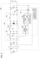
- the power conversion device 100 includes an AC voltage input unit 10, a class-E power conversion circuit 20, a current sensor 60, and a control unit 50.
- a load 1 and an AC power supply 2 are connected to the power conversion device 100.
- the class-E power conversion circuit 20 has a class-E inverter circuit 30 and a rectifier circuit 40.
- the class-E inverter circuit 30 has an input choke inductor 31, a switch 32, a shunt capacitor 33 connected in parallel with the switch 32, and an LC resonance circuit 34.
- a high-frequency alternating current is generated by the switch 32 repeatedly turning the high-frequency on and off.
- the switch 32 is constituted by, for example, a semiconductor transistor such as a Metal-Oxide-Semiconductor Field-Effect Transistor (MOSFET).
- MOSFET Metal-Oxide-Semiconductor Field-Effect Transistor
- a capacitor of a single component may be arranged as the shunt capacitor 33 connected in parallel with the switch 32. However, the capacitor may not be arranged as a separate component by utilizing the parasitic capacitance of the MOSFET used as the switch.
- the rectifier circuit 40 rectifies a high-frequency current generated by the class-E inverter circuit 30.
- the rectifier circuit 40 has a diode, a rectifier side shunt capacitor connected in parallel to the diode, and an output choke inductor.
- a so-called “class-E rectifier” may be arranged as the rectifier circuit 40.
- a so-called “class D rectifier” consisting of four diodes connected by a bridge may be arranged as the rectifier circuit 40.
- the turn-on loss of the class-E power conversion circuit 20 occurs due to the principle described below.
- the switch 32 is switched from off to on, the shunt capacitor 33 is short-circuited by the switch 32, and the electrostatic energy stored in the shunt capacitor 33 is converted to Joule heat by the switch 32.
- the class-E power conversion circuit 20 performs so-called "zero voltage switching (ZVS)" in which the turn-on loss is reduced to zero by using the current of the LC resonance circuit 34 to reduce both end voltages of the switch 32 to zero when the switch 32 is turned off and then turning on the switch 32.
- ZVS zero voltage switching
- the zero voltage switching allows to reduce the loss even when the operating frequency is increased to a higher frequency, thereby making it possible to decrease the size of the power conversion device 100.
- the zero voltage switching operation of the class-E power conversion circuit 20 is not unconditionally established, and whether or not it is established can be determined by various conditions such as input voltage, output voltage, input current, output current, switching frequency, and On-Duty of the switch 32. If the zero voltage switching is not established, a large turn-on loss occurs in the class-E power conversion circuit 20. Therefore, until now, the class-E power conversion circuit 20 is not used in applications where the input/output conditions change greatly.
- a voltage adjusting means is installed to stabilize the input/output conditions as in the prior art. However, as described above, the installation of the voltage adjusting means leads to the enlargement of the power conversion device.
- the output current of the class-E power conversion circuit 20 is detected, and the On-Duty of the switch control signal is set based on the detected output current.
- the current sensor 60 detects the output current of the class-E power conversion circuit 20.
- the control unit 50 sets the On-Duty of the switch control signal based on the output current detected by the current sensor 60.
- the control unit 50 includes a command value generation unit 51, a comparison unit 52, an On-Duty setting unit 53, and a signal generation unit 54.
- the command value generation unit 51 uses a current value that should be supplied to the load 1 as the output current command value and outputs it to the comparison unit 52.
- the signal generation unit 54 generates a control signal so that the measured value and the command value become the value, and outputs it to the switch 32. Since these functions constitute a well-known feedback control, a detailed description thereof is omitted.
- the On-Duty means a ratio of an ON section to a sum of the ON section and an OFF section, that is, the ratio of the ON section in one cycle.
- a horizontal axis indicates the input voltage of the class-E power conversion circuit 20
- the vertical axis indicates the switching frequency of the class-E power conversion circuit 20.
- values of the horizontal axis are from 0 V to 283 V, which represent the absolute values in the variation range of the input voltage when the input voltage is 200 V AC.
- the power conversion device 100 will be described as controlling the input current to a high power factor.
- Controlling the power factor to a high power factor means controlling the power factor to approach 1.
- an operation trajectory of the class-E power conversion circuit 20 when the power factor of the input current becomes 1 is superposed on a contour plot of the turn-on loss when the On-Duty is operated at 0.55, that is, the input current becomes sinusoidal like the input voltage.
- Reference sign 70 denotes the operation trajectory when the average output current is 2 A
- reference sign 71 denotes the operation trajectory when the average output current is 4 A
- reference sign 72 denotes the operation trajectory when the average output current is 6 A
- reference sign 73 denotes the operation trajectory when the average output current is 8 A.
- a region denoted by reference sign 80 is the region in which the zero voltage switching is not established.
- a region denoted by reference sign 81 indicates that the turn-on loss becomes zero, and is the region in which the zero voltage switching is established under the condition that the voltage Vton at both ends of the switch 32 when it is turned on is zero.
- the operation trajectories of the average output currents of 8 A (reference sign 73) and 6 A (reference sign 72) all pass through the region 81 in which the zero voltage switching is possible between 0 V and 283 V, which is the voltage fluctuation range of 200 V AC, and it can be seen that the zero voltage switching is possible in all regions in response to changes in AC voltages of 50 Hz and 60 Hz.
- the operation trajectories of the average output current of 2 A (reference sign 70) and 4 A (reference sign 71) partly pass through the region 80 in which the zero voltage switching not established. Therefore, it can be seen that under the conditions of the average output current of 2 A and 4 A, the zero voltage switching cannot be established in all regions in response to the changes of AC input voltages of 50 Hz and 60 Hz.
- the On-Duty is made smaller than in FIG. 2 . Specifically, in FIG. 3 , the On-Duty is operated at 0.45. Under this On-Duty condition, it is impossible to draw a trajectory such that the average output current is 8 A (reference sign 73). That is, under the condition that the average output current is 8 A, the class-E power conversion circuit 20 cannot operate.
- FIG. 3 similarly to FIG. 2 , it can be seen that the switch driving frequency of the class-E power conversion circuit 20 is required to be shifted to a lower frequency as the average output current increases to 2 A (reference sign 70), 4 A (reference sign 71), and 6 A (reference sign 72). Comparing the zero voltage switching region (region 81) in FIG.
- an operation trajectory having an average output current of 4 A (reference sign 71) and 2 A (reference sign 70) passes through a region 81 in which the zero voltage switching can be established between 0 V and 283 V, and by changing the On-Duty from 0.55 to 0.45, it is possible to establish the zero voltage switching in all regions in response to changes in AC voltages even under conditions of average output currents of 2 A and 4 A, in which the zero voltage switching could not be established in all regions when the On-Duty is 0.55.
- the drive frequency of the switch 32 is changed to a higher frequency in order to reduce the average value of the output current.
- a new operation in which the zero voltage switching region can be shifted to a higher frequency when the On-Duty is reduced can be used. For example, when the On-Duty is reduced from 0.55 to 0.45, even under the condition that the average output current is 2 A, the zero voltage switching can be established in all regions of the voltage variation range from 0 V to 283 V AC.
- the class-E power conversion circuit 20 has the class-E inverter circuit 30 and the rectifier circuit 40 connected to the class-E inverter circuit 30 and rectifying the high-frequency alternating current generated by the class-E inverter circuit 30 to a direct current or a low-frequency AC voltage.
- the class-E inverter circuit 30 includes the AC voltage input unit 10 into which an AC voltage is input, the switch 32 for switching the current on/off, the input choke inductor 31 connected to at least one end of the switch 32 and the AC voltage input unit 10, and the LC resonance circuit 34 connected to the rectifier circuit 40.
- the control unit 50 sets the On-Duty of the switch 32 based on the output current or output power output from the class-E power conversion circuit 20.
- the control trajectory of the switch driving frequency of the class-E power conversion circuit 20 tends to shift to a lower frequency.
- the region in which the zero voltage switching is established shifts to a lower frequency. Therefore, it is possible to establish the zero voltage switching in a wide range of the output current or the output power and to reduce the loss by detecting the magnitude of the output power or the output current and increasing the On-Duty of the switch 32 when the output power increases.
- the controller 50 may set the On-Duty based on the measured value of the output current or the output power output from the class-E power conversion circuit 20.
- the On-Duty that is suitable under the operating conditions of the actual class-E power conversion circuit 20 at that point by setting the On-Duty based on a measured value of the output power or the output current.
- the output current is detected, and the On-Duty is set based on the detected output current.
- the same effect can be obtained when the output voltage is detected separately, and the On-Duty is set based on the output power obtained by multiplying the output voltage and the output current.
- the second embodiment differs from the first embodiment in that the On-Duty setting unit 53 sets the On-Duty based on the command value (command value of the output current) acquired from the command value generation unit 51.
- the description of the configuration overlapping with the first embodiment is omitted by referring to the reference signs. The following description will focus on the differences.
- On-Duty of the switch control signal of the class-E power conversion circuit 20 is set based on the command value of the output current.
- the load 1 is connected to the output of the power conversion device 100, such as a battery with a very stable voltage.
- the output voltage of the power conversion device 100 is dominantly determined by the state of the load 1, and the power conversion device 100 controls the output current or output power.
- the control unit 50 sets the current value that should be supplied to the load 1 as the output current command value, and generates a control signal so that the output current measurement value and the output current command value become the value.
- the cutoff frequency of the current sensor 60 for detecting the output current can be controlled even at a frequency as low as, for example, 1/100 compared to the frequency of the switch control signal of the class-E power conversion circuit 20. Since it is sufficient to be higher than 100 Hz, the cutoff frequency of about 10 kHz can be controlled, and when the class-E power conversion circuit 20 is operated at, for example, 1 MHz, the relationship between these frequencies is about 1 to 100. However, when a current sensor with such a low cutoff frequency is used, the measured value has a great delay with respect to the current value of the output current. In the second embodiment, by setting the On-Duty based on the output current command value, it is possible to establish the zero voltage switching without using an expensive current sensor and without affected by the delay of the measured value.
- the control unit 50 sets the On-Duty based on the command value of the output current or output power.
- the On-Duty can be set in advance by performing control to change the output current or output power of the class-E power converter 20. Without being affected by the delay in detection of the output current or output power, the zero voltage switching can be maintained and the loss can be reduced.
- the power conversion device 100 has a voltage sensor 61 as shown in FIG. 5 .
- the On-Duty setting unit 53 sets the On-Duty of the switch control signal of the class-E power conversion circuit 20 based on the output power that is a product of the output voltage of the class-E power conversion circuit 20 detected by the voltage sensor 61 and the output current of the class-E power conversion circuit 20 detected by the current sensor 60.
- FIG. 6 is a map of the class-E power conversion circuit 20 according to the third embodiment, in which it is evaluated whether the zero voltage switching can be established in all regions within the variation range of AC input voltage with respect to the value of On-Duty and the average value of output power.
- the power conversion device 100 according to the third embodiment sets the On-Duty so that the zero voltage switching can be established at a present output power average value.
- the map of FIG. 6 will be described below.
- the average output power is shown at 0.5 kW, 1 kW, 2 kW and 3 kW.
- a map in Fig. 6 is the map when the average output power is evaluated in combination with On-Duty. This evaluation is carried out in advance. The evaluation is performed by changing the average output power and the On-Duty in a wider range with higher resolution in the range in which the power conversion device 100 may be used and creating a map in advance, so that a more suitable On-Duty can be set in the evaluation.
- the output power average value is a value between the resolutions of the output power average value of the map evaluated in advance, it is possible to set the On-Duty with a high probability that the zero voltage switching can be established in all regions within the variation range of the AC input voltage by interpolating the value.
- the control unit 50 sets the On-Duty based on a relationship between the output current or the output power, and whether the zero voltage switching is achievable. Specifically, the control unit 50 sets the value of the On-Duty so that the zero voltage switching can be achieved in all regions of an input voltage range under the output power condition under which the class-E power conversion circuit 20 is at present operating, based on the relationship obtained by evaluating in advance whether the zero voltage switching can be established with respect to the average output power value and the value of the On-Duty. Thus, even if the output voltage of the class-E power conversion circuit 20 changes, the zero voltage switching can be maintained in a wide range within the variation range of the AC voltage, thereby reducing the loss.
- the power conversion device 100 sets the On-Duty of the switch control signal of the class-E power conversion circuit 20 based on the output power that is the product of the output current and the output voltage of the class-E power conversion circuit 20 and the output voltage of the class-E power conversion circuit 20.
- the On-Duty that can establish the zero voltage switching in all regions within the variation range of the AC input voltage changes, even if the output power average value is the same.
- the On-Duty is set based of a map in which whether the zero voltage switching can be established is evaluated in advance not only for the output current but also for the output voltage.
- the On-Duty is changed to, for example, 0.40 under the condition that the output voltage Vout is 260 V, it is possible to establish the zero voltage switching within the variation range of the AC input voltage even in the operation trajectory in which the output power average value is 0.5 kW.
- FIG. 8 shows, as an example, a map for evaluating combinations of the output voltage Vout of 260 V, 340 V, and 420 V, the average output power of 0.5 kW, 1 kW, 2 kW, and 3 kW, and the On-Duty of 0.35, 0.40, 0.45, 0.50, 0.55, and 0.60.
- the evaluation is performed by changing the average output power and the On-Duty in a wider range with higher resolution in the range in which the power conversion device 100 may be used and creating a map in advance, so that a more suitable On-Duty can be set in the evaluation.
- the output voltage and the output power average value are a value between the resolutions of the map evaluated in advance, it is possible to set the On-Duty with a high probability that the zero voltage switching can be established in all regions within the variation range of the AC input voltage by interpolating the value.
- the control unit 50 sets the On-Duty based on the output voltage output from the class-E power conversion circuit 20.
- the control unit 50 sets the value of the On-Duty based on the output voltage when the regions of zero voltage switching and the trajectory of the control frequency change depending on the output voltage.
- the control unit 50 may set the On-Duty based on a relationship between the output voltage, the output current or the output power, and whether the zero voltage switching can be established. Thus, even if the output voltage and the output power of the class-E power conversion circuit 20 change, the zero voltage switching can be maintained in a wide range within the variation range of the AC voltage, thereby reducing the loss.
- the power conversion device 100 has a voltage sensor 61 and a voltage sensor 62 as shown in FIG. 9 .
- the AC input voltage of the class-E power conversion circuit 20 is also taken into consideration to set the On-Duty of the switch control signal of the class-E power conversion circuit 20.
- the On-Duty that can establish the zero voltage switching in all regions within the variation range of the AC input voltage changes, even if the output voltage and the output power average value are the same.
- the On-Duty is set based on a map in which whether the zero voltage switching can be established is evaluated in advance not only for the output power and the output voltage but also for the AC input voltage.
- the zero voltage switching region can be established within the variation range of the AC input voltage in the operation trajectory with the output power average value of 1 kW.
- FIG. 10 shows, as an example, a map for evaluating combinations of the AC input voltage Vin of AC200 V and AC240 V, the output voltage Vout of 260 V, 340 V, 420 V, the average output power of 0.5 kW, 1 kW, 2 kW, and 3 kW, and the On-Duty of 0.35, 0.40, 0.45, 0.50, 0.55, and 0.60.
- the evaluation is performed by changing the average output power and the On-Duty in a wider range with higher resolution in the range in which the power conversion device 100 may be used and creating a map in advance, so that a more suitable On-Duty can be set in the evaluation.
- the output voltage and the output power average value are a value between the resolutions of the map evaluated in advance, it is possible to set the On-Duty with a high probability that the zero voltage switching can be established in all regions within the variation range of the AC input voltage by interpolating the value.
- the control unit 50 sets the On-Duty based on an AC voltage value input to the AC voltage input unit 10.
- the control unit 50 sets the On-Duty based on the AC input voltage.
- a suitable On-Duty can be set with the value of the present AC input voltage. Even when connected to different AC input voltages depending on the country, region, and the like, the zero voltage switching can be established, thereby reducing the loss.
- the control unit 50 may set the On-Duty based on a relationship between the AC voltage value input to the AC voltage input unit 10, the output current or output power, and whether the zero voltage switching can be established. Thus, even if the AC input voltage of the class-E power conversion circuit 20 changes, the zero voltage switching can be established in a wide range within the variation range of the AC voltage, thereby reducing the loss.
Landscapes
- Engineering & Computer Science (AREA)
- Power Engineering (AREA)
- Dc-Dc Converters (AREA)
- Inverter Devices (AREA)
Abstract
Description
- The present invention relates to a power conversion method and a power conversion device.
- Conventionally, there has been known an invention that enables a class-E power conversion circuit to operate with high efficiency over a wide input range (Patent Literature 1). The invention described in
Patent Literature 1 enables a class-E power conversion circuit to operate with high efficiency over a wide input range by arranging a voltage adjusting means for stabilizing an input voltage of the class-E power conversion circuit between the class-E power conversion circuit and an AC input voltage. - Patent Literature 1:
Japanese Patent Publication No. 2018-196271 - However, in the invention described in
Patent Literature 1, it is necessary to provide an additional voltage adjusting means, resulting in increasing the size of a power conversion device. - The present invention has been made in view of the above problem, and an object thereof is to provide a power conversion method and a power conversion device which can operate at high efficiency without increasing the size.
- The power conversion method according to one aspect of the present invention sets the On-Duty of the switch based on an output current or output power output from the class-E power conversion circuit.
- According to the present invention, the power conversion device can operate at high efficiency without increasing in size.
-
- [
FIG. 1] FIG. 1 is a configuration diagram of apower conversion device 100 according to a first embodiment of the present invention. - [
FIG. 2] FIG. 2 is a graph showing a relationship between an input voltage and a switching frequency. - [
FIG. 3] FIG. 3 is a graph showing a relationship between an input voltage and a switching frequency. - [
FIG. 4] FIG. 4 is a configuration diagram of thepower conversion device 100 according to a second embodiment of the present invention. - [
FIG. 5] FIG. 5 is a configuration diagram of thepower conversion device 100 according to a third embodiment of the present invention. - [
FIG. 6] FIG. 6 is a map showing whether the zero voltage switching can be established. - [
FIG. 7] FIG. 7 is a configuration diagram of thepower conversion device 100 according to a fourth embodiment of the present invention. - [
FIG. 8] FIG. 8 is a map showing whether the zero voltage switching can be established. - [
FIG. 9] FIG. 9 is a configuration diagram of thepower conversion device 100 according to a fifth embodiment of the present invention. - [
FIG. 10] FIG. 10 is amap 10 showing whether the zero voltage switching can be established. - Embodiments of the present invention will now be described with reference to the drawings. In the description of the drawings, the same parts are denoted by the same reference signs and the description thereof is omitted.
- The configuration of the
power conversion device 100 according to a first embodiment will be described with reference toFIG. 1 . As shown inFIG. 1 , thepower conversion device 100 includes an ACvoltage input unit 10, a class-Epower conversion circuit 20, acurrent sensor 60, and acontrol unit 50. Aload 1 and anAC power supply 2 are connected to thepower conversion device 100. The class-Epower conversion circuit 20 has a class-E inverter circuit 30 and arectifier circuit 40. - The class-
E inverter circuit 30 has aninput choke inductor 31, aswitch 32, ashunt capacitor 33 connected in parallel with theswitch 32, and anLC resonance circuit 34. A high-frequency alternating current is generated by theswitch 32 repeatedly turning the high-frequency on and off. Theswitch 32 is constituted by, for example, a semiconductor transistor such as a Metal-Oxide-Semiconductor Field-Effect Transistor (MOSFET). A capacitor of a single component may be arranged as theshunt capacitor 33 connected in parallel with theswitch 32. However, the capacitor may not be arranged as a separate component by utilizing the parasitic capacitance of the MOSFET used as the switch. - The
rectifier circuit 40 rectifies a high-frequency current generated by the class-E inverter circuit 30. Therectifier circuit 40 has a diode, a rectifier side shunt capacitor connected in parallel to the diode, and an output choke inductor. A so-called "class-E rectifier" may be arranged as therectifier circuit 40. A so-called "class D rectifier" consisting of four diodes connected by a bridge may be arranged as therectifier circuit 40. - It is generally known that the higher the operating frequency of the class-E
power conversion circuit 20, the smaller the inductance and capacitance values required for passive components to be used such as inductors and capacitors. By utilizing this phenomenon, it is possible to decrease the size of thepower conversion device 100. However, in order to operate the class-Epower conversion circuit 20 at high frequency and high efficiency, it is necessary to reduce a turn-on loss that occurs when switching theswitch 32 from off to on. - The turn-on loss of the class-E
power conversion circuit 20 occurs due to the principle described below. When theswitch 32 is switched from off to on, theshunt capacitor 33 is short-circuited by theswitch 32, and the electrostatic energy stored in theshunt capacitor 33 is converted to Joule heat by theswitch 32. A switching loss Psw is then expressed byFormula 1 using the capacitance Cs of theshunt capacitor 33 and the voltage Vton at both ends of theswitch 32 at the moment when theswitch 32 is switched from off to on.
[Mathematical 1]
- The class-E
power conversion circuit 20 performs so-called "zero voltage switching (ZVS)" in which the turn-on loss is reduced to zero by using the current of theLC resonance circuit 34 to reduce both end voltages of theswitch 32 to zero when theswitch 32 is turned off and then turning on theswitch 32. The zero voltage switching allows to reduce the loss even when the operating frequency is increased to a higher frequency, thereby making it possible to decrease the size of thepower conversion device 100. - However, the zero voltage switching operation of the class-E
power conversion circuit 20 is not unconditionally established, and whether or not it is established can be determined by various conditions such as input voltage, output voltage, input current, output current, switching frequency, and On-Duty of theswitch 32. If the zero voltage switching is not established, a large turn-on loss occurs in the class-Epower conversion circuit 20. Therefore, until now, the class-Epower conversion circuit 20 is not used in applications where the input/output conditions change greatly. When it is used, a voltage adjusting means is installed to stabilize the input/output conditions as in the prior art. However, as described above, the installation of the voltage adjusting means leads to the enlargement of the power conversion device. - Therefore, in the present embodiment, the output current of the class-E
power conversion circuit 20 is detected, and the On-Duty of the switch control signal is set based on the detected output current. As shown inFIG. 1 , thecurrent sensor 60 detects the output current of the class-Epower conversion circuit 20. Thecontrol unit 50 sets the On-Duty of the switch control signal based on the output current detected by thecurrent sensor 60. Specifically, thecontrol unit 50 includes a commandvalue generation unit 51, acomparison unit 52, an On-Duty setting unit 53, and asignal generation unit 54. As an example, the commandvalue generation unit 51 uses a current value that should be supplied to theload 1 as the output current command value and outputs it to thecomparison unit 52. Thesignal generation unit 54 generates a control signal so that the measured value and the command value become the value, and outputs it to theswitch 32. Since these functions constitute a well-known feedback control, a detailed description thereof is omitted. The On-Duty means a ratio of an ON section to a sum of the ON section and an OFF section, that is, the ratio of the ON section in one cycle. - Next, an operation example of the class-E
power conversion circuit 20 will be described with reference toFIG. 2 and 3 . InFIG. 2 , a horizontal axis indicates the input voltage of the class-Epower conversion circuit 20, and the vertical axis indicates the switching frequency of the class-Epower conversion circuit 20. InFIG. 2 , values of the horizontal axis are from 0 V to 283 V, which represent the absolute values in the variation range of the input voltage when the input voltage is 200 V AC. Here, in a power conversion device that draws power from a general AC power system, it is required to control the input current to the highest power factor possible. In the following, unless otherwise specified, thepower conversion device 100 will be described as controlling the input current to a high power factor. "Controlling the power factor to a high power factor" means controlling the power factor to approach 1. In the graph shown inFIG. 2 , an operation trajectory of the class-Epower conversion circuit 20 when the power factor of the input current becomes 1 is superposed on a contour plot of the turn-on loss when the On-Duty is operated at 0.55, that is, the input current becomes sinusoidal like the input voltage. -
Reference sign 70 denotes the operation trajectory when the average output current is 2 A,reference sign 71 denotes the operation trajectory when the average output current is 4 A,reference sign 72 denotes the operation trajectory when the average output current is 6 A, andreference sign 73 denotes the operation trajectory when the average output current is 8 A. A region denoted byreference sign 80 is the region in which the zero voltage switching is not established. A region denoted byreference sign 81 indicates that the turn-on loss becomes zero, and is the region in which the zero voltage switching is established under the condition that the voltage Vton at both ends of theswitch 32 when it is turned on is zero. - From the graph shown in
FIG. 2 , it can be seen that as an average output current increases to 2 A (reference sign 70), 4 A (reference sign 71), 6 A (reference sign 72), and 8 A (reference sign 73), a switch driving frequency of the class-Epower conversion circuit 20 is required to be shifted to a lower frequency. Under the condition that the On-Duty is 0.55, the operation trajectories of the average output currents of 8 A (reference sign 73) and 6 A (reference sign 72) all pass through theregion 81 in which the zero voltage switching is possible between 0 V and 283 V, which is the voltage fluctuation range of 200 V AC, and it can be seen that the zero voltage switching is possible in all regions in response to changes in AC voltages of 50 Hz and 60 Hz. On the other hand, the operation trajectories of the average output current of 2 A (reference sign 70) and 4 A (reference sign 71) partly pass through theregion 80 in which the zero voltage switching not established. Therefore, it can be seen that under the conditions of the average output current of 2 A and 4 A, the zero voltage switching cannot be established in all regions in response to the changes of AC input voltages of 50 Hz and 60 Hz. - In
FIG. 3 , the On-Duty is made smaller than inFIG. 2 . Specifically, inFIG. 3 , the On-Duty is operated at 0.45. Under this On-Duty condition, it is impossible to draw a trajectory such that the average output current is 8 A (reference sign 73). That is, under the condition that the average output current is 8 A, the class-Epower conversion circuit 20 cannot operate. InFIG. 3 , similarly toFIG. 2 , it can be seen that the switch driving frequency of the class-Epower conversion circuit 20 is required to be shifted to a lower frequency as the average output current increases to 2 A (reference sign 70), 4 A (reference sign 71), and 6 A (reference sign 72). Comparing the zero voltage switching region (region 81) inFIG. 2 with the zero voltage switching region (region 81) inFIG. 3 , it can be seen that the zero voltage switching region (region 81) can be shifted to a high frequency when the On-Duty is changed from 0.55 to a smaller 0.45. This is the operation revealed by the inventors of the present invention. InFIG. 3 , a part of an operation trajectory having an average output current of 6 A (reference sign 72) passes through theregion 80 in which the zero voltage switching cannot be established, and therefore the zero voltage switching cannot be established in all regions in response to changes in AC voltage. On the other hand, an operation trajectory having an average output current of 4 A (reference sign 71) and 2 A (reference sign 70) passes through aregion 81 in which the zero voltage switching can be established between 0 V and 283 V, and by changing the On-Duty from 0.55 to 0.45, it is possible to establish the zero voltage switching in all regions in response to changes in AC voltages even under conditions of average output currents of 2 A and 4 A, in which the zero voltage switching could not be established in all regions when the On-Duty is 0.55. - In the class-E
power conversion circuit 20 according to the first embodiment, when an operation state in which the average output current is 8 A, the On-Duty is 0.55, and the zero voltage switching is established in all regions of an AC voltage variation range from 0 V to 283 V is changed to a state in which the average output current is 2 A, the drive frequency of theswitch 32 is changed to a higher frequency in order to reduce the average value of the output current. A new operation in which the zero voltage switching region can be shifted to a higher frequency when the On-Duty is reduced can be used. For example, when the On-Duty is reduced from 0.55 to 0.45, even under the condition that the average output current is 2 A, the zero voltage switching can be established in all regions of the voltage variation range from 0 V to 283 V AC. - As described above, according to the
power conversion device 100 according to the first embodiment, the following operation and effect can be obtained. - The class-E
power conversion circuit 20 has the class-E inverter circuit 30 and therectifier circuit 40 connected to the class-E inverter circuit 30 and rectifying the high-frequency alternating current generated by the class-E inverter circuit 30 to a direct current or a low-frequency AC voltage. The class-E inverter circuit 30 includes the ACvoltage input unit 10 into which an AC voltage is input, theswitch 32 for switching the current on/off, theinput choke inductor 31 connected to at least one end of theswitch 32 and the ACvoltage input unit 10, and theLC resonance circuit 34 connected to therectifier circuit 40. Thecontrol unit 50 sets the On-Duty of theswitch 32 based on the output current or output power output from the class-Epower conversion circuit 20. In the class-Epower conversion circuit 20 connected to the AC voltage, when a larger power or current is required to be output, for example, when the output voltage drops due to a variation in theload 1 or thecontrol unit 50 is instructed to supply a larger power from the outside, the control trajectory of the switch driving frequency of the class-Epower conversion circuit 20 tends to shift to a lower frequency. In the class-Epower conversion circuit 20 connected to the AC voltage, when the On-Duty of theswitch 32 is increased, the region in which the zero voltage switching is established shifts to a lower frequency. Therefore, it is possible to establish the zero voltage switching in a wide range of the output current or the output power and to reduce the loss by detecting the magnitude of the output power or the output current and increasing the On-Duty of theswitch 32 when the output power increases. - Further, the
controller 50 may set the On-Duty based on the measured value of the output current or the output power output from the class-Epower conversion circuit 20. In an application in which the current drawn by theload 1 connected to thepower conversion device 100 is determined independent of the state of thepower conversion device 100, it is possible to set the On-Duty that is suitable under the operating conditions of the actual class-Epower conversion circuit 20 at that point by setting the On-Duty based on a measured value of the output power or the output current. Thus, even in a transient state in which a fluctuation of the load current occurs, the zero voltage switching can be maintained, and the loss can be reduced. - In the first embodiment, the output current is detected, and the On-Duty is set based on the detected output current. However, the same effect can be obtained when the output voltage is detected separately, and the On-Duty is set based on the output power obtained by multiplying the output voltage and the output current.
- Next, a second embodiment of the present invention will be described with reference to
FIG. 4 . The second embodiment differs from the first embodiment in that the On-Duty setting unit 53 sets the On-Duty based on the command value (command value of the output current) acquired from the commandvalue generation unit 51. The description of the configuration overlapping with the first embodiment is omitted by referring to the reference signs. The following description will focus on the differences. - In the second embodiment, On-Duty of the switch control signal of the class-E
power conversion circuit 20 is set based on the command value of the output current. For example, when thepower conversion device 100 is used for an application such as a battery charger, theload 1 is connected to the output of thepower conversion device 100, such as a battery with a very stable voltage. At this time, the output voltage of thepower conversion device 100 is dominantly determined by the state of theload 1, and thepower conversion device 100 controls the output current or output power. For example, when thepower conversion device 100 controls the output current as shown inFIG. 4 , thecontrol unit 50 sets the current value that should be supplied to theload 1 as the output current command value, and generates a control signal so that the output current measurement value and the output current command value become the value. However, when controlling the output current in an application such as a battery charger, the cutoff frequency of thecurrent sensor 60 for detecting the output current can be controlled even at a frequency as low as, for example, 1/100 compared to the frequency of the switch control signal of the class-Epower conversion circuit 20. Since it is sufficient to be higher than 100 Hz, the cutoff frequency of about 10 kHz can be controlled, and when the class-Epower conversion circuit 20 is operated at, for example, 1 MHz, the relationship between these frequencies is about 1 to 100. However, when a current sensor with such a low cutoff frequency is used, the measured value has a great delay with respect to the current value of the output current. In the second embodiment, by setting the On-Duty based on the output current command value, it is possible to establish the zero voltage switching without using an expensive current sensor and without affected by the delay of the measured value. - As described above, in the second embodiment, the
control unit 50 sets the On-Duty based on the command value of the output current or output power. In an application such as a battery charger in which thepower conversion device 100 itself controls the current or power supplied to theload 1, by setting the On-Duty based on the command value of the output current or output power, the On-Duty can be set in advance by performing control to change the output current or output power of the class-E power converter 20. Without being affected by the delay in detection of the output current or output power, the zero voltage switching can be maintained and the loss can be reduced. In addition, there is no need to use a current sensor or a voltage sensor which can detect up to a high frequency band for detecting the fluctuation of the output current or output power, thereby contributing to the cost reduction. - Next, a third embodiment of the present invention will be described with reference to
FIGS. 5 and6 . Thepower conversion device 100 according to the third embodiment has avoltage sensor 61 as shown inFIG. 5 . The On-Duty setting unit 53 sets the On-Duty of the switch control signal of the class-Epower conversion circuit 20 based on the output power that is a product of the output voltage of the class-Epower conversion circuit 20 detected by thevoltage sensor 61 and the output current of the class-Epower conversion circuit 20 detected by thecurrent sensor 60. -
FIG. 6 is a map of the class-Epower conversion circuit 20 according to the third embodiment, in which it is evaluated whether the zero voltage switching can be established in all regions within the variation range of AC input voltage with respect to the value of On-Duty and the average value of output power. Referring to the map shown inFIG. 6 , thepower conversion device 100 according to the third embodiment sets the On-Duty so that the zero voltage switching can be established at a present output power average value. Thus, it is possible to set a suitable On-Duty which can reduce the turn-on loss of the present average output power. The map ofFIG. 6 will be described below. The average output power is shown at 0.5 kW, 1 kW, 2 kW and 3 kW. The values of the On-Duty are shown at 0.35, 0.40, 0.45, 0.50, 0.55 and 0.60. A map inFig. 6 is the map when the average output power is evaluated in combination with On-Duty. This evaluation is carried out in advance. The evaluation is performed by changing the average output power and the On-Duty in a wider range with higher resolution in the range in which thepower conversion device 100 may be used and creating a map in advance, so that a more suitable On-Duty can be set in the evaluation. Furthermore, when the output power average value is a value between the resolutions of the output power average value of the map evaluated in advance, it is possible to set the On-Duty with a high probability that the zero voltage switching can be established in all regions within the variation range of the AC input voltage by interpolating the value. - As described above, in the third embodiment, the
control unit 50 sets the On-Duty based on a relationship between the output current or the output power, and whether the zero voltage switching is achievable. Specifically, thecontrol unit 50 sets the value of the On-Duty so that the zero voltage switching can be achieved in all regions of an input voltage range under the output power condition under which the class-Epower conversion circuit 20 is at present operating, based on the relationship obtained by evaluating in advance whether the zero voltage switching can be established with respect to the average output power value and the value of the On-Duty. Thus, even if the output voltage of the class-Epower conversion circuit 20 changes, the zero voltage switching can be maintained in a wide range within the variation range of the AC voltage, thereby reducing the loss. - Next, a fourth embodiment of the present invention will be described with reference to
FIGS. 7 and8 . As shown inFIG. 7 , thepower conversion device 100 according to the fourth embodiment sets the On-Duty of the switch control signal of the class-Epower conversion circuit 20 based on the output power that is the product of the output current and the output voltage of the class-Epower conversion circuit 20 and the output voltage of the class-Epower conversion circuit 20.FIG. 8 is a map of the class-Epower conversion circuit 20 according to the fourth embodiment, in which it is evaluated whether the zero voltage switching can be established in all regions within the variation range of the AC input voltage for the output DC voltage (Vout=260 V, 340 V, 420 V), the value of the On-Duty, and the output power average value. As shown inFIG. 8 , when the output voltage of the class-Epower conversion circuit 20 changes, the On-Duty that can establish the zero voltage switching in all regions within the variation range of the AC input voltage changes, even if the output power average value is the same. In thepower conversion device 100 according to the fourth embodiment, the On-Duty is set based of a map in which whether the zero voltage switching can be established is evaluated in advance not only for the output current but also for the output voltage. Thus, it is possible to set a suitable On-Duty that can reduce the turn-on loss of the average output power at present even when the output voltage changes. - For example, when the output voltage Vout is 340 V and the output power average value is 0.5 kW, the zero voltage switching is established in all regions within the variation range of the AC input voltage by setting the On-Duty to 0.45. On the other hand, when the output voltage Vout is 260 V and the output power average value is 0.5 kW, the zero voltage switching is not established in some regions within the variation range of the AC input voltage by setting the On-Duty to 0.45. When the On-Duty is changed to, for example, 0.40 under the condition that the output voltage Vout is 260 V, it is possible to establish the zero voltage switching within the variation range of the AC input voltage even in the operation trajectory in which the output power average value is 0.5 kW.
-
FIG. 8 shows, as an example, a map for evaluating combinations of the output voltage Vout of 260 V, 340 V, and 420 V, the average output power of 0.5 kW, 1 kW, 2 kW, and 3 kW, and the On-Duty of 0.35, 0.40, 0.45, 0.50, 0.55, and 0.60. The evaluation is performed by changing the average output power and the On-Duty in a wider range with higher resolution in the range in which thepower conversion device 100 may be used and creating a map in advance, so that a more suitable On-Duty can be set in the evaluation. Furthermore, when the output voltage and the output power average value are a value between the resolutions of the map evaluated in advance, it is possible to set the On-Duty with a high probability that the zero voltage switching can be established in all regions within the variation range of the AC input voltage by interpolating the value. - As described above, in the fourth embodiment, the
control unit 50 sets the On-Duty based on the output voltage output from the class-Epower conversion circuit 20. In the class-Epower conversion circuit 20 connected to the AC voltage, thecontrol unit 50 sets the value of the On-Duty based on the output voltage when the regions of zero voltage switching and the trajectory of the control frequency change depending on the output voltage. Thus, it is possible to set a suitable On-Duty at the present output voltage, and the zero voltage switching can be maintained even when the output voltage changes, thereby reducing the loss. - The
control unit 50 may set the On-Duty based on a relationship between the output voltage, the output current or the output power, and whether the zero voltage switching can be established. Thus, even if the output voltage and the output power of the class-Epower conversion circuit 20 change, the zero voltage switching can be maintained in a wide range within the variation range of the AC voltage, thereby reducing the loss. - Next, a fifth embodiment of the present invention will be described with reference to FIGA. 9 and 10. The
power conversion device 100 according to the fifth embodiment has avoltage sensor 61 and avoltage sensor 62 as shown inFIG. 9 . In the fifth embodiment, in addition to the output current of the class-Epower conversion circuit 20 and the output voltage of the class-Epower conversion circuit 20, the AC input voltage of the class-Epower conversion circuit 20 is also taken into consideration to set the On-Duty of the switch control signal of the class-Epower conversion circuit 20. -
FIG. 10 is a map of the class-Epower conversion circuit 20 according to the fifth embodiment, in which it is evaluated whether the zero voltage switching can be established in all regions within the variation range of the AC input voltage for the AC input voltage (Vin=AC 200 V, 240 V), the output DC voltage (Vout=260 V, 340 V, 420 V), the value of the On-Duty, and the output power average value. - As shown in
FIG. 10 , when the AC input voltage of the class-Epower conversion circuit 20 changes, the On-Duty that can establish the zero voltage switching in all regions within the variation range of the AC input voltage changes, even if the output voltage and the output power average value are the same. In thepower conversion device 100 according to the fifth embodiment, the On-Duty is set based on a map in which whether the zero voltage switching can be established is evaluated in advance not only for the output power and the output voltage but also for the AC input voltage. Thus, it is possible to set a suitable On-Duty that can reduce the turn-on loss at the present average output power even when the output voltage changes. - For example, when connected to a power system with AC input voltage Vin=AC200 V, the On-Duty is set to 0.50 with the output voltage Vout of 340 V and the output power average value of 1 kW to be operated in all regions within the variation range of the AC input voltage operates in the establishment regions of the zero voltage switching. On the other hand, if the ON duty is similarly operated at 0.50 when the power system is connected to the AC input voltage Vin= 240 V AC, and the output voltage Vout is 340 V and the average output power value is 1 kW, there is a region where 0 voltage switching is not established within the variation range of the AC input voltage. When the On-Duty is changed to 0.45 under the condition of the AC input voltage Vin=AC100 V and the output voltage Vout=340 V, the zero voltage switching region can be established within the variation range of the AC input voltage in the operation trajectory with the output power average value of 1 kW.
-
FIG. 10 shows, as an example, a map for evaluating combinations of the AC input voltage Vin of AC200 V and AC240 V, the output voltage Vout of 260 V, 340 V, 420 V, the average output power of 0.5 kW, 1 kW, 2 kW, and 3 kW, and the On-Duty of 0.35, 0.40, 0.45, 0.50, 0.55, and 0.60. The evaluation is performed by changing the average output power and the On-Duty in a wider range with higher resolution in the range in which thepower conversion device 100 may be used and creating a map in advance, so that a more suitable On-Duty can be set in the evaluation. Furthermore, when the output voltage and the output power average value are a value between the resolutions of the map evaluated in advance, it is possible to set the On-Duty with a high probability that the zero voltage switching can be established in all regions within the variation range of the AC input voltage by interpolating the value. - As described above, in the fifth embodiment, the
control unit 50 sets the On-Duty based on an AC voltage value input to the ACvoltage input unit 10. In the class-Epower conversion circuit 20 connected to the AC voltage, when the region of the zero voltage switching and the trajectory of the control frequency change depending on the value of the AC input voltage, thecontrol unit 50 sets the On-Duty based on the AC input voltage. As a result, a suitable On-Duty can be set with the value of the present AC input voltage. Even when connected to different AC input voltages depending on the country, region, and the like, the zero voltage switching can be established, thereby reducing the loss. - The
control unit 50 may set the On-Duty based on a relationship between the AC voltage value input to the ACvoltage input unit 10, the output current or output power, and whether the zero voltage switching can be established. Thus, even if the AC input voltage of the class-Epower conversion circuit 20 changes, the zero voltage switching can be established in a wide range within the variation range of the AC voltage, thereby reducing the loss. - Embodiments of the present invention are described as above, but it should not be understood that the description and drawings that form part of this disclosure are intended to limit the present invention. The disclosure will reveal to those skilled in the art a variety of alternative embodiments, examples, and operating techniques.
-
- 100
- Power conversion device
- 10
- AC voltage input unit
- 20
- Class-E power conversion circuit
- 30
- Class-E inverter circuit
- 31
- Input choke inductor
- 32
- Switch
- 33
- Shunt capacitor
- 34
- LC resonant circuit
- 40
- Rectifier circuit
- 50
- Control unit
Claims (10)
- A power conversion method for a power conversion device having a class-E power conversion circuit, wherein:the class-E power conversion circuit has a class-E inverter circuit and a rectifier circuit connected to the class-E inverter circuit and rectifying a high-frequency alternating current generated by the class-E inverter circuit to a direct current or a low-frequency AC voltage;the class-E inverter circuit comprises an AC voltage input unit into which an AC voltage is input, a switch for switching the current on/off, an input choke inductor connected to at least one end of the switch and the AC voltage input unit, and an LC resonance circuit connected to the rectifier circuit; comprisingsetting an On-Duty of the switch based on an output current or output power output from the class-E power conversion circuit.
- The power conversion method according to claim 1, comprising increasing the On-Duty as the output current or the output power is increased.
- The power conversion method according to claim 1 or 2, comprising setting the On-Duty based on a measured value of the output current or the output power.
- The power conversion method according to claim 1 or 2, comprising setting the On-Duty based on a command value of the output current or the output power.
- The power conversion method according to any one of claims 1 to 4, comprising setting the On-Duty based on a relationship between the output current or the output power, and whether the zero voltage switching is achievable.
- The power conversion method according to any one of claims 1 to 5, comprising setting the On-Duty based on an output voltage output from the class-E power conversion circuit.
- The power conversion method according to claim 6, comprising setting the On-Duty based on a relationship between the output voltage, the output current or the output power, and whether the zero voltage switching is achievable.
- The power conversion method according to any one of claims 1 to 7, comprising setting the On-Duty based on an AC voltage value input to the AC voltage input unit.
- The power conversion method according to claim 8, comprising setting the On-Duty based on a relationship between the AC voltage value, the output current or the output power, and whether the zero voltage switching can be established.
- A power conversion device having a class-E power conversion circuit, wherein:the class-E power conversion circuit has a class-E inverter circuit and a rectifier circuit connected to the class-E inverter circuit and rectifying a high-frequency alternating current generated by the class-E inverter circuit to a direct current or a low-frequency AC voltage;the class-E inverter circuit comprises an AC voltage input unit into which an AC voltage is input, a switch for switching the current on/off, an input choke inductor connected to at least one end of the switch and the AC voltage input unit, and an LC resonance circuit connected to the rectifier circuit; andan On-Duty of the switch is set based on an output current or output power output from the class-E power conversion circuit.
Applications Claiming Priority (1)
| Application Number | Priority Date | Filing Date | Title |
|---|---|---|---|
| PCT/IB2022/000092 WO2023161669A1 (en) | 2022-02-22 | 2022-02-22 | Electric-power conversion method and electric-power conversion device |
Publications (2)
| Publication Number | Publication Date |
|---|---|
| EP4485785A1 true EP4485785A1 (en) | 2025-01-01 |
| EP4485785A4 EP4485785A4 (en) | 2025-03-26 |
Family
ID=87764904
Family Applications (1)
| Application Number | Title | Priority Date | Filing Date |
|---|---|---|---|
| EP22927605.0A Pending EP4485785A4 (en) | 2022-02-22 | 2022-02-22 | Electric-power conversion method and electric-power conversion device |
Country Status (5)
| Country | Link |
|---|---|
| US (1) | US20250167660A1 (en) |
| EP (1) | EP4485785A4 (en) |
| JP (1) | JP7825700B2 (en) |
| CN (1) | CN119032500A (en) |
| WO (1) | WO2023161669A1 (en) |
Family Cites Families (17)
| Publication number | Priority date | Publication date | Assignee | Title |
|---|---|---|---|---|
| JP4624686B2 (en) * | 2004-01-15 | 2011-02-02 | 株式会社ダイヘン | High frequency power supply |
| US20090129134A1 (en) * | 2005-09-12 | 2009-05-21 | Koninklijke Philips Electronics, N.V. | Controlled class-e dc ac converter |
| JP2013030973A (en) | 2011-07-28 | 2013-02-07 | Nippon Soken Inc | Power supply device, contactless power transmission device, vehicle, and contactless power transmission system |
| US8736368B2 (en) * | 2011-08-16 | 2014-05-27 | Qualcomm Incorporated | Class E amplifier overload detection and prevention |
| WO2015158699A1 (en) * | 2014-04-15 | 2015-10-22 | Danmarks Tekniske Universitet | A resonant dc-dc power converter assembly |
| JP2015211393A (en) * | 2014-04-28 | 2015-11-24 | 旭化成エレクトロニクス株式会社 | Power amplifier circuit |
| US9941799B1 (en) * | 2014-08-08 | 2018-04-10 | Flextronics Ap, Llc | Cascade power system with isolated Class-E resonant circuit |
| JP6834366B2 (en) | 2016-11-04 | 2021-02-24 | 船井電機株式会社 | Power supply |
| JP6712547B2 (en) * | 2016-12-27 | 2020-06-24 | 株式会社京三製作所 | Power supply device and power supply device control method |
| JP6763315B2 (en) * | 2017-02-02 | 2020-09-30 | Tdk株式会社 | Switching power supply |
| JP2018196271A (en) | 2017-05-19 | 2018-12-06 | パナソニックIpマネジメント株式会社 | Power conversion device |
| WO2019171510A1 (en) | 2018-03-07 | 2019-09-12 | 日産自動車株式会社 | Method for controlling resonant power conversion device, resonant power conversion device, and dc-dc converter |
| WO2019202352A1 (en) | 2018-04-20 | 2019-10-24 | 日産自動車株式会社 | Control method for controlling resonant power converter, and resonant power converter |
| JP7206452B2 (en) * | 2018-07-03 | 2023-01-18 | 国立大学法人千葉大学 | POWER CONVERSION DEVICE AND CONTROL METHOD FOR POWER CONVERSION DEVICE |
| CN114128120B (en) | 2019-07-12 | 2022-12-20 | 日产自动车株式会社 | Power conversion device and control method thereof |
| JP7325059B2 (en) | 2020-03-11 | 2023-08-14 | 日産自動車株式会社 | Power factor correction circuit |
| JP7664086B2 (en) | 2021-05-28 | 2025-04-17 | 日産自動車株式会社 | Method for controlling power converter and power converter |
-
2022
- 2022-02-22 WO PCT/IB2022/000092 patent/WO2023161669A1/en not_active Ceased
- 2022-02-22 JP JP2024502575A patent/JP7825700B2/en active Active
- 2022-02-22 CN CN202280092393.6A patent/CN119032500A/en active Pending
- 2022-02-22 EP EP22927605.0A patent/EP4485785A4/en active Pending
- 2022-02-22 US US18/840,415 patent/US20250167660A1/en active Pending
Also Published As
| Publication number | Publication date |
|---|---|
| US20250167660A1 (en) | 2025-05-22 |
| CN119032500A (en) | 2024-11-26 |
| JPWO2023161669A1 (en) | 2023-08-31 |
| EP4485785A4 (en) | 2025-03-26 |
| WO2023161669A1 (en) | 2023-08-31 |
| JP7825700B2 (en) | 2026-03-06 |
Similar Documents
| Publication | Publication Date | Title |
|---|---|---|
| US10770979B2 (en) | LLC resonant converter | |
| CN104052293B (en) | Multiphase DC/DC Converter | |
| US9774269B2 (en) | Bidirectional DC/DC converter | |
| KR100632094B1 (en) | Resonance type switching power source | |
| US8817494B2 (en) | PFC AC/DC converter reducing harmonics, switching loss, and switching noise | |
| CN101212856A (en) | Cold cathode fluorescent lamp inverter apparatus | |
| US20120163037A1 (en) | Resonant converter | |
| US9912241B2 (en) | System and method for a cascode switch | |
| KR20190043268A (en) | Dc-dc converter | |
| JP2018121473A (en) | Power converter | |
| EP2579434A2 (en) | Rectifier with power factor correction | |
| US20110051462A1 (en) | Power factor improvement circuit | |
| EP3944482B1 (en) | Method for controlling power conversion device, and power conversion device | |
| US9433060B2 (en) | Power factor correction circuit, operating device for a light-emitting means and method for controlling a power factor correction circuit | |
| JP4217950B2 (en) | Control method of DC / DC converter | |
| US11316423B2 (en) | Half-bridge having power semiconductors | |
| US20100226152A1 (en) | Inverter | |
| EP3319232A1 (en) | Power source apparatus | |
| US20180041116A1 (en) | Quasi-Resonant Power Converter with Reduced Dynamic Switching Losses | |
| US20250167660A1 (en) | Power conversion method and power conversion device | |
| JP4635584B2 (en) | Switching power supply | |
| US6798674B2 (en) | Half-bridge converter with high power factor | |
| US11664733B2 (en) | Control method of a flyback power converter | |
| KR20180109796A (en) | DC/DC Converter circuit of switching regulator | |
| JP5105819B2 (en) | DC-DC converter |
Legal Events
| Date | Code | Title | Description |
|---|---|---|---|
| STAA | Information on the status of an ep patent application or granted ep patent |
Free format text: STATUS: THE INTERNATIONAL PUBLICATION HAS BEEN MADE |
|
| PUAI | Public reference made under article 153(3) epc to a published international application that has entered the european phase |
Free format text: ORIGINAL CODE: 0009012 |
|
| STAA | Information on the status of an ep patent application or granted ep patent |
Free format text: STATUS: REQUEST FOR EXAMINATION WAS MADE |
|
| 17P | Request for examination filed |
Effective date: 20240822 |
|
| AK | Designated contracting states |
Kind code of ref document: A1 Designated state(s): AL AT BE BG CH CY CZ DE DK EE ES FI FR GB GR HR HU IE IS IT LI LT LU LV MC MK MT NL NO PL PT RO RS SE SI SK SM TR |
|
| A4 | Supplementary search report drawn up and despatched |
Effective date: 20250220 |
|
| RIC1 | Information provided on ipc code assigned before grant |
Ipc: H02M 7/04 20060101ALI20250217BHEP Ipc: H02M 3/156 20060101ALI20250217BHEP Ipc: H02M 3/00 20060101ALI20250217BHEP Ipc: H02M 1/10 20060101ALI20250217BHEP Ipc: H02M 1/00 20060101ALI20250217BHEP Ipc: H02M 7/48 20070101AFI20250217BHEP |
|
| DAV | Request for validation of the european patent (deleted) | ||
| DAX | Request for extension of the european patent (deleted) |