EP4485407A1 - Banknote-image-processing device and banknote-image-processing method - Google Patents
Banknote-image-processing device and banknote-image-processing method Download PDFInfo
- Publication number
- EP4485407A1 EP4485407A1 EP22928577.0A EP22928577A EP4485407A1 EP 4485407 A1 EP4485407 A1 EP 4485407A1 EP 22928577 A EP22928577 A EP 22928577A EP 4485407 A1 EP4485407 A1 EP 4485407A1
- Authority
- EP
- European Patent Office
- Prior art keywords
- image
- processing
- banknote
- processor
- damage
- Prior art date
- Legal status (The legal status is an assumption and is not a legal conclusion. Google has not performed a legal analysis and makes no representation as to the accuracy of the status listed.)
- Withdrawn
Links
Images







Classifications
-
- G—PHYSICS
- G07—CHECKING-DEVICES
- G07D—HANDLING OF COINS OR VALUABLE PAPERS, e.g. TESTING, SORTING BY DENOMINATIONS, COUNTING, DISPENSING, CHANGING OR DEPOSITING
- G07D7/00—Testing specially adapted to determine the identity or genuineness of valuable papers or for segregating those which are unacceptable, e.g. banknotes that are alien to a currency
- G07D7/181—Testing mechanical properties or condition, e.g. wear or tear
- G07D7/189—Detecting attached objects, e.g. tapes or clips
-
- G—PHYSICS
- G06—COMPUTING OR CALCULATING; COUNTING
- G06T—IMAGE DATA PROCESSING OR GENERATION, IN GENERAL
- G06T11/00—Two-dimensional [2D] image generation
- G06T11/60—Creating or editing images; Combining images with text
-
- G—PHYSICS
- G07—CHECKING-DEVICES
- G07D—HANDLING OF COINS OR VALUABLE PAPERS, e.g. TESTING, SORTING BY DENOMINATIONS, COUNTING, DISPENSING, CHANGING OR DEPOSITING
- G07D7/00—Testing specially adapted to determine the identity or genuineness of valuable papers or for segregating those which are unacceptable, e.g. banknotes that are alien to a currency
- G07D7/06—Testing specially adapted to determine the identity or genuineness of valuable papers or for segregating those which are unacceptable, e.g. banknotes that are alien to a currency using wave or particle radiation
- G07D7/12—Visible light, infrared or ultraviolet radiation
-
- G—PHYSICS
- G07—CHECKING-DEVICES
- G07D—HANDLING OF COINS OR VALUABLE PAPERS, e.g. TESTING, SORTING BY DENOMINATIONS, COUNTING, DISPENSING, CHANGING OR DEPOSITING
- G07D7/00—Testing specially adapted to determine the identity or genuineness of valuable papers or for segregating those which are unacceptable, e.g. banknotes that are alien to a currency
- G07D7/16—Testing the dimensions
- G07D7/164—Thickness
-
- G—PHYSICS
- G07—CHECKING-DEVICES
- G07D—HANDLING OF COINS OR VALUABLE PAPERS, e.g. TESTING, SORTING BY DENOMINATIONS, COUNTING, DISPENSING, CHANGING OR DEPOSITING
- G07D7/00—Testing specially adapted to determine the identity or genuineness of valuable papers or for segregating those which are unacceptable, e.g. banknotes that are alien to a currency
- G07D7/181—Testing mechanical properties or condition, e.g. wear or tear
- G07D7/183—Detecting folds or doubles
-
- G—PHYSICS
- G07—CHECKING-DEVICES
- G07D—HANDLING OF COINS OR VALUABLE PAPERS, e.g. TESTING, SORTING BY DENOMINATIONS, COUNTING, DISPENSING, CHANGING OR DEPOSITING
- G07D7/00—Testing specially adapted to determine the identity or genuineness of valuable papers or for segregating those which are unacceptable, e.g. banknotes that are alien to a currency
- G07D7/181—Testing mechanical properties or condition, e.g. wear or tear
- G07D7/185—Detecting holes or pores
-
- G—PHYSICS
- G07—CHECKING-DEVICES
- G07D—HANDLING OF COINS OR VALUABLE PAPERS, e.g. TESTING, SORTING BY DENOMINATIONS, COUNTING, DISPENSING, CHANGING OR DEPOSITING
- G07D7/00—Testing specially adapted to determine the identity or genuineness of valuable papers or for segregating those which are unacceptable, e.g. banknotes that are alien to a currency
- G07D7/181—Testing mechanical properties or condition, e.g. wear or tear
- G07D7/187—Detecting defacement or contamination, e.g. dirt
Definitions
- the present disclosure relates to a banknote image processing device and a banknote image processing method.
- banknote identification algorithms and banknote identification systems using images of banknotes needs, in addition to images of normal banknotes, a large number of images of abnormal banknotes with damages (hereinafter also referred to as "damaged banknote images"), such as a banknote with a hole, a partially cut banknote, a torn banknote, a folded banknote, a stained banknote, and a washed banknote.
- damaged banknote images such as a banknote with a hole, a partially cut banknote, a torn banknote, a folded banknote, a stained banknote, and a washed banknote.
- Patent Literature 1 Japanese Patent Application Laid-open No. 2011-258029
- the present disclosure proposes a technique to easily obtain a large number of damaged banknote images.
- a banknote image processing device of the present disclosure includes a storage unit and a processor.
- the storage unit stores an image of a normal banknote therein.
- the processor performs pseudo-damage processing that imitates damage caused on the normal banknote, on the image.
- FIG. 1 is a diagram illustrating a structure example of a banknote image processing system in Example 1 according to the present disclosure.
- a banknote image processing system 1 includes a banknote image processing device 10, an input device 20, and a display 30.
- the input device 20 and the display 30 are connected to the banknote image processing device 10.
- Examples of the input device 20 include a pointing device such as a mouse, and a keyboard.
- Examples of the display 30 include a liquid crystal display (LCD).
- the banknote image processing device 10 includes a processor 11 and a storage unit 12.
- the processor 11 include a central processing unit (CPU), a digital signal processor (DSP), a field programmable gate array (FPGA), and an application specific integrated circuit (ASIC).
- the storage unit 12 include a memory and a storage.
- the banknote image processing device 10 is realized by, for example, a computer.
- the storage unit 12 stores therein in advance images that are captured by a camera (hereinafter also referred to as “captured images”), including images of normal banknotes that have no damage (hereinafter also referred to as “normal banknote images”).
- the captured images include an image of an obverse side of a normal banknote (hereinafter also referred to as “obverse image”) and an image of a reverse side of the normal banknote (hereinafter also referred to as "reverse image”).
- FIG. 2 is a diagram illustrating one example of the captured image in Example 1 according to the present disclosure.
- a captured image OI is formed from a normal banknote image MOIa and an image of the background of the normal banknote (hereinafter also referred to as "background image") BI.
- the normal banknote image MOIa is a rectangular image, with corner points C1, C2, C3, and C4 corresponding to four vertices of the rectangle.
- the processor 11 acquires the captured image OI from the storage unit 12 and performs pseudo damage processing (hereinafter also referred to as "pseudo-damage processing"), which imitates damages to be caused on the normal banknotes, on the normal banknote image MOIa included in the acquired captured image OI, thereby generating a damaged banknote image.
- pseudo damage processing hereinafter also referred to as "pseudo-damage processing”
- processed image the image formed from the damaged banknote image and the background image BI, i.e., the image obtained by performing the pseudo-damage processing on the normal banknote image MOIa is called “processed image” in some cases.
- FIG. 3 is a diagram illustrating one example of the normalized projection in Example 1 according to the present disclosure.
- the processor 11 detects the four corner points C1 to C4 of the normal banknote image MOIa and performs the normalized projection on the basis of the detected corner points C1 to C4.
- the image after the normalized projection is referred to as "normalized image” in some cases.
- the width of a normalized image MOIb is expressed as "W” and the height of the normalized image MOIb is expressed as "H".
- the processor 11 When any pseudo-damage processing described below is performed on the normal banknote image MOIa, the processor 11 also performs the normalized projection as a pre-treatment of the pseudo-damage processing and performs back projection of the normalized projection as a post-treatment of the pseudo-damage processing.
- the normalized projection As a pre-treatment of the pseudo-damage processing and performs back projection of the normalized projection as a post-treatment of the pseudo-damage processing.
- Each of hole processing, cutting processing, tearing processing, corner folding processing, staining processing, and washing processing will be described below as examples of the pseudo-damage processing.
- FIG. 4 and FIG. 5 are diagrams illustrating an example of the hole processing in Example 1 according to the present disclosure.
- the processor 11 acquires the pixel values of the background image BI (hereinafter also referred to as "background pixel values") from the normalized image MOIb.
- the processor 11 converts the pixel values of a circular region HL with a radius R whose center is at a center coordinate (Cx, Cy), into the background pixel values, as illustrated in FIG. 4 .
- the center coordinate (Cx, Cy) and the radius R are designated by the operator of the banknote image processing system 1 using the input device 20.
- the hole processing is performed on the normal banknote image MOIa as the pseudo-damage processing for the normal banknote image MOIa.
- a processed image Ia including a damaged banknote image MIa with a hole HLI as illustrated in FIG. 5 is obtained.
- FIG. 6 and FIG. 7 are diagrams illustrating an example of the cutting processing in Example 1 according to the present disclosure.
- the processor 11 acquires the background pixel values from the normalized image MOIb.
- the processor 11 calculates the x-coordinate, based on designated lengths L1 and L2 according to Equation (1), as illustrated in FIG. 6 .
- the designated lengths L1 and L2 are designated by the operator of the banknote image processing system 1 using the input device 20.
- the processor 11 then converts the pixel values from the coordinate (0, y) to the x-coordinate expressed by Equation (1) into the background pixel values. Note that the processor 11 changes the y-coordinate in Equation (1) in the range of 0 to H - 1 line by line.
- x L2 ⁇ L1 / H ⁇ 1 ⁇ y + L1 ⁇ 1
- the cutting processing is performed on the normal banknote image MOIa as the pseudo-damage processing for the normal banknote image MOIa, and as illustrated in FIG. 7 , a processed image Ib including a damaged banknote image MIb in which a part CUI of the normal banknote image MOIa is cut from the normal banknote image MOIa is obtained.
- FIG. 8 and FIG. 9 are diagrams illustrating an example of the tearing processing in Example 1 according to the present disclosure.
- the processor 11 acquires the background pixel values from the normalized image MOIb.
- the processor 11 calculates the vertex coordinate (Vx, Vy) on the basis of designated lengths P and L and an angle A according to Equations (2) and (3) as illustrated in FIG. 8 .
- the processor 11 also calculates B1 and B2 coordinates on the basis of designated lengths P and BL according to Equations (4) and (5) as illustrated in FIG. 8 .
- the designated lengths P, L, and BL and the angle A are designated by the operator of the banknote image processing system 1 using the input device 20.
- Vx P + L ⁇ sin A
- Vy H ⁇ L ⁇ cos
- B1 P ⁇ BL / 2 ⁇ 1
- B2 P + BL / 2 ⁇ 1
- the processor 11 then converts the pixel values from the x1-coordinate expressed by Equation (6) to the x2-coordinate expressed by Equation (7), starting from the vertex coordinate (Vx, Vy), into the background pixel values. Note that the processor 11 changes the y-coordinate in Equations (6) and (7) in the range of Vy to H - 1 line by line.
- the pixel values in a region TE surrounded by the segments BL, L1, and L2 are converted into the background pixel values. Accordingly, the tearing processing is performed on the normal banknote image MOIa as the pseudo-damage processing for the normal banknote image MOIa and as illustrated in FIG. 9 , a processed image Ic including a damaged banknote image MIc in which a tear TEI exists in a part of the normal banknote image MOIa is obtained.
- FIG. 10 and FIG. 11 are diagrams illustrating an example of the corner folding processing in Example 1 according to the present disclosure.
- the processor 11 acquires the background pixel values from the normalized image MOIb.
- the processor 11 calculates an angle ⁇ , a rotation angle ⁇ , an x-axis direction travel distance Tx, and a y-axis direction travel distance Ty, based on designated lengths Dx and Dy according to Equations (8), (9), (10) and (11), as illustrated in FIG. 10 .
- the designated lengths Dx and Dy are designated by the operator of the banknote image processing system 1 using the input device 20.
- the processor 11 also rotates the reverse image in the range from the coordinate (0, y) to the x-coordinate expressed by Equation (12) by the rotation angle ⁇ and moves the reverse image by the travel distances Tx and Ty before attaching the reverse image onto the obverse image.
- the processor 11 also converts the pixel values from the coordinate (0, y) to the x-coordinate expressed by Equation (13) into the background pixel values. Note that the processor 11 changes the y-coordinate in Equations (12) and (13) in the range of 0 to Dy line by line.
- the corner folding processing is performed on the normal banknote image MOIa as the pseudo-damage processing for the normal banknote image MOIa and as illustrated in FIG. 11 , a processed image Id including a damaged banknote image MId in which a corner folding FOI exists in a part of the normal banknote image MOIa is obtained.
- FIG. 12 and FIG. 13 are diagrams illustrating an example of the staining processing in Example 1 according to the present disclosure.
- the processor 11 calculates the coordinate (X1, Y1) and the coordinate (X2, Y2) on the basis of the center coordinate (Cx, Cy) and the designated length L according to Equations (14), (15), (16), (17), and (18) as illustrated in FIG. 12 .
- the center coordinate (Cx, Cy) and the designated length L are designated by the operator of the banknote image processing system 1 using the input device 20.
- R L / 2
- X 1 Cx ⁇
- R Y 1 Cy ⁇
- the processor 11 then reduces the luminance of the pixels in a region ST by multiplying the pixel values in the region ST from the coordinate (X1, Y1) to the coordinate (X2, Y2) by a predetermined gain value.
- the staining processing is performed on the normal banknote image MOIa as the pseudo-damage processing for the normal banknote image MOIa, and as illustrated in FIG. 13 , a processed image Ie including a damaged banknote image MIe in which a stain STI exists in a part of the normal banknote image MOIa is obtained.
- Laundry detergents contain fluorescent agents. Therefore, an image of a washed banknote will be brighter than an image of a normal, unwashed banknote.
- the processor 11 increases the luminance of all pixels in the normalized image MOIb by multiplying the pixel values of all pixels in the normalized image MOIb by a predetermined gain value.
- the washing processing is performed on the normal banknote image MOIa as the pseudo-damage processing for the normal banknote image MOIa, and a processed image including a damaged banknote image with the increased brightness of the entire normal banknote image MOIa is obtained.
- Example 1 has been described above.
- Example 2 a case in which a tape is attached to a banknote is described.
- FIG. 14 and FIG. 15 are diagrams illustrating one example of thickness data in Example 2 according to the present disclosure.
- FIG. 14 illustrates the thickness data in the height H direction
- FIG. 15 illustrates the thickness data in the width W direction.
- data OD represents thickness data indicating the thickness of the normal banknote
- data TZ represents thickness data indicating the thickness of the tape attached to the banknote
- "WD" in FIG. 14 represents the height of the tape.
- the tape with the thickness TZ and the height WD is attached to an X1 position in the height H direction on the normal banknote with the thickness OD.
- FIG. 15 it is assumed that the tape is attached to the position a little to the right in the width W direction on the normal banknote.
- the processor 11 adds the thickness data TZ, which represents the thickness of the tape, to the thickness data OD, which represents the thickness of the normal banknote, based on the designated value X1.
- the designated value X1 is designated by the operator of the banknote image processing system 1 using the input device 20.
- the thickness data OD and TZ are stored in the storage unit 12 in advance.
- the processor 11 adds the thickness data of the tape to the thickness data of the normal banknote in this manner, thereby generating the thickness data of the abnormal banknote with the tape attached.
- Example 2 has been described above.
- the banknote image processing device includes the storage unit (storage unit 12 in Examples) and the processor (processor 11 in Examples).
- the storage unit stores the images of the normal banknotes therein.
- the processor performs the pseudo-damage processing, which imitates the damage caused on the normal banknote, on the image of the normal banknote.
- the processor performs the hole processing on the image of the normal banknote as the pseudo-damage processing.
- the processor performs the cutting processing on the image of the normal banknote as the pseudo-damage processing.
- the processor performs the tearing processing on the image of the normal banknote as the pseudo-damage processing.
- the processor performs the corner folding processing on the image of the normal banknote as the pseudo-damage processing.
- the processor performs the staining processing on the image of the normal banknote as the pseudo-damage processing.
- the processor performs the washing processing on the image of the normal banknote as the pseudo-damage processing.
- the damaged banknote images can be generated by simply processing the images of the normal banknotes without actually damaging the real banknotes; therefore, a large number of damaged banknote images can be easily obtained.
Landscapes
- Physics & Mathematics (AREA)
- General Physics & Mathematics (AREA)
- Engineering & Computer Science (AREA)
- Theoretical Computer Science (AREA)
- Health & Medical Sciences (AREA)
- General Health & Medical Sciences (AREA)
- Toxicology (AREA)
- Inspection Of Paper Currency And Valuable Securities (AREA)
Abstract
Description
- The present disclosure relates to a banknote image processing device and a banknote image processing method.
- Development of banknote identification algorithms and banknote identification systems using images of banknotes needs, in addition to images of normal banknotes, a large number of images of abnormal banknotes with damages (hereinafter also referred to as "damaged banknote images"), such as a banknote with a hole, a partially cut banknote, a torn banknote, a folded banknote, a stained banknote, and a washed banknote.
- Patent Literature 1:
Japanese Patent Application Laid-open No. 2011-258029 - However, obtaining a large number of damaged banknote images by actually damaging the real banknotes would need a great deal of workloads to perform damage processing on the real banknotes.
- In view of this, the present disclosure proposes a technique to easily obtain a large number of damaged banknote images.
- A banknote image processing device of the present disclosure includes a storage unit and a processor. The storage unit stores an image of a normal banknote therein. The processor performs pseudo-damage processing that imitates damage caused on the normal banknote, on the image.
- According to the art disclosed herein, a large number of damaged banknote images can be obtained easily.
-
-
FIG. 1 is a diagram illustrating a structure example of a banknote image processing system in Example 1 according to the present disclosure. -
FIG. 2 is a diagram illustrating one example of a captured image in Example 1 according to the present disclosure. -
FIG. 3 is a diagram illustrating one example of normalized projection in Example 1 according to the present disclosure. -
FIG. 4 is a diagram illustrating one example of hole processing in Example 1 according to the present disclosure. -
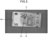
FIG. 5 is a diagram illustrating one example of the hole processing in Example 1 according to the present disclosure. -
FIG. 6 is a diagram illustrating one example of cutting processing in Example 1 according to the present disclosure. -
FIG. 7 is a diagram illustrating one example of the cutting processing in Example 1 according to the present disclosure. -
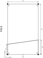
FIG. 8 is a diagram illustrating one example of tearing processing in Example 1 according to the present disclosure. -
FIG. 9 is a diagram illustrating one example of the tearing processing in Example 1 according to the present disclosure. -
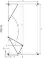
FIG. 10 is a diagram illustrating one example of corner folding processing in Example 1 according to the present disclosure. -
FIG. 11 is a diagram illustrating one example of the corner folding processing in Example 1 according to the present disclosure. -
FIG. 12 is a diagram illustrating one example of staining processing in Example 1 according to the present disclosure. -
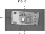
FIG. 13 is a diagram illustrating one example of the staining processing in Example 1 according to the present disclosure. -
FIG. 14 is a diagram illustrating one example of thickness data in Example 2 according to the present disclosure. -
FIG. 15 is a diagram illustrating one example of the thickness data in Example 2 according to the present disclosure. - Examples of the present disclosure will be described below based on the drawings. In Examples below, the same structures are denoted with the same reference sign.
-
FIG. 1 is a diagram illustrating a structure example of a banknote image processing system in Example 1 according to the present disclosure. - In
FIG. 1 , a banknoteimage processing system 1 includes a banknoteimage processing device 10, aninput device 20, and adisplay 30. Theinput device 20 and thedisplay 30 are connected to the banknoteimage processing device 10. Examples of theinput device 20 include a pointing device such as a mouse, and a keyboard. Examples of thedisplay 30 include a liquid crystal display (LCD). - The banknote
image processing device 10 includes a processor 11 and astorage unit 12. Examples of the processor 11 include a central processing unit (CPU), a digital signal processor (DSP), a field programmable gate array (FPGA), and an application specific integrated circuit (ASIC). Examples of thestorage unit 12 include a memory and a storage. The banknoteimage processing device 10 is realized by, for example, a computer. - The
storage unit 12 stores therein in advance images that are captured by a camera (hereinafter also referred to as "captured images"), including images of normal banknotes that have no damage (hereinafter also referred to as "normal banknote images"). The captured images include an image of an obverse side of a normal banknote (hereinafter also referred to as "obverse image") and an image of a reverse side of the normal banknote (hereinafter also referred to as "reverse image"). -
FIG. 2 is a diagram illustrating one example of the captured image in Example 1 according to the present disclosure. InFIG. 2 , a captured image OI is formed from a normal banknote image MOIa and an image of the background of the normal banknote (hereinafter also referred to as "background image") BI. The normal banknote image MOIa is a rectangular image, with corner points C1, C2, C3, and C4 corresponding to four vertices of the rectangle. - The processor 11 acquires the captured image OI from the
storage unit 12 and performs pseudo damage processing (hereinafter also referred to as "pseudo-damage processing"), which imitates damages to be caused on the normal banknotes, on the normal banknote image MOIa included in the acquired captured image OI, thereby generating a damaged banknote image. In the following description, the image formed from the damaged banknote image and the background image BI, i.e., the image obtained by performing the pseudo-damage processing on the normal banknote image MOIa is called "processed image" in some cases. - The processor 11 performs normalized projection on the normal banknote image MOIa before performing the pseudo-damage processing on the normal banknote image MOIa.
FIG. 3 is a diagram illustrating one example of the normalized projection in Example 1 according to the present disclosure. As illustrated inFIG. 3 , the processor 11 detects the four corner points C1 to C4 of the normal banknote image MOIa and performs the normalized projection on the basis of the detected corner points C1 to C4. In the following description, the image after the normalized projection is referred to as "normalized image" in some cases. InFIG. 3 , the width of a normalized image MOIb is expressed as "W" and the height of the normalized image MOIb is expressed as "H". When any pseudo-damage processing described below is performed on the normal banknote image MOIa, the processor 11 also performs the normalized projection as a pre-treatment of the pseudo-damage processing and performs back projection of the normalized projection as a post-treatment of the pseudo-damage processing. Each of hole processing, cutting processing, tearing processing, corner folding processing, staining processing, and washing processing will be described below as examples of the pseudo-damage processing. -
FIG. 4 andFIG. 5 are diagrams illustrating an example of the hole processing in Example 1 according to the present disclosure. First, the processor 11 acquires the pixel values of the background image BI (hereinafter also referred to as "background pixel values") from the normalized image MOIb. Next, the processor 11 converts the pixel values of a circular region HL with a radius R whose center is at a center coordinate (Cx, Cy), into the background pixel values, as illustrated inFIG. 4 . The center coordinate (Cx, Cy) and the radius R are designated by the operator of the banknoteimage processing system 1 using theinput device 20. By converting the pixel values of the circular region HL with the radius R into the background pixel values, the hole processing is performed on the normal banknote image MOIa as the pseudo-damage processing for the normal banknote image MOIa. Thus, a processed image Ia including a damaged banknote image MIa with a hole HLI as illustrated inFIG. 5 is obtained. -
FIG. 6 andFIG. 7 are diagrams illustrating an example of the cutting processing in Example 1 according to the present disclosure. First, the processor 11 acquires the background pixel values from the normalized image MOIb. Next, the processor 11 calculates the x-coordinate, based on designated lengths L1 and L2 according to Equation (1), as illustrated inFIG. 6 . The designated lengths L1 and L2 are designated by the operator of the banknoteimage processing system 1 using theinput device 20. The processor 11 then converts the pixel values from the coordinate (0, y) to the x-coordinate expressed by Equation (1) into the background pixel values. Note that the processor 11 changes the y-coordinate in Equation (1) in the range of 0 to H - 1 line by line.
- By converting the pixel values of a region CU with the designated lengths L1 and L2 and the height H into the background pixel values, the cutting processing is performed on the normal banknote image MOIa as the pseudo-damage processing for the normal banknote image MOIa, and as illustrated in
FIG. 7 , a processed image Ib including a damaged banknote image MIb in which a part CUI of the normal banknote image MOIa is cut from the normal banknote image MOIa is obtained. -
FIG. 8 andFIG. 9 are diagrams illustrating an example of the tearing processing in Example 1 according to the present disclosure. First, the processor 11 acquires the background pixel values from the normalized image MOIb. Next, the processor 11 calculates the vertex coordinate (Vx, Vy) on the basis of designated lengths P and L and an angle A according to Equations (2) and (3) as illustrated inFIG. 8 . The processor 11 also calculates B1 and B2 coordinates on the basis of designated lengths P and BL according to Equations (4) and (5) as illustrated inFIG. 8 . The designated lengths P, L, and BL and the angle A are designated by the operator of the banknoteimage processing system 1 using theinput device 20.


- The processor 11 then converts the pixel values from the x1-coordinate expressed by Equation (6) to the x2-coordinate expressed by Equation (7), starting from the vertex coordinate (Vx, Vy), into the background pixel values. Note that the processor 11 changes the y-coordinate in Equations (6) and (7) in the range of Vy to H - 1 line by line.


- Thus, the pixel values in a region TE surrounded by the segments BL, L1, and L2 are converted into the background pixel values. Accordingly, the tearing processing is performed on the normal banknote image MOIa as the pseudo-damage processing for the normal banknote image MOIa and as illustrated in
FIG. 9 , a processed image Ic including a damaged banknote image MIc in which a tear TEI exists in a part of the normal banknote image MOIa is obtained. -
FIG. 10 andFIG. 11 are diagrams illustrating an example of the corner folding processing in Example 1 according to the present disclosure. First, the processor 11 acquires the background pixel values from the normalized image MOIb. Next, the processor 11 calculates an angle θ, a rotation angle ϕ, an x-axis direction travel distance Tx, and a y-axis direction travel distance Ty, based on designated lengths Dx and Dy according to Equations (8), (9), (10) and (11), as illustrated inFIG. 10 . The designated lengths Dx and Dy are designated by the operator of the banknoteimage processing system 1 using theinput device 20.



- The processor 11 also rotates the reverse image in the range from the coordinate (0, y) to the x-coordinate expressed by Equation (12) by the rotation angle ϕ and moves the reverse image by the travel distances Tx and Ty before attaching the reverse image onto the obverse image. The processor 11 also converts the pixel values from the coordinate (0, y) to the x-coordinate expressed by Equation (13) into the background pixel values. Note that the processor 11 changes the y-coordinate in Equations (12) and (13) in the range of 0 to Dy line by line.


- Thus, the obverse image in a region F01 is converted into the reverse image and the pixel values of a region F02 are converted into the background pixel values. Therefore, the corner folding processing is performed on the normal banknote image MOIa as the pseudo-damage processing for the normal banknote image MOIa and as illustrated in
FIG. 11 , a processed image Id including a damaged banknote image MId in which a corner folding FOI exists in a part of the normal banknote image MOIa is obtained. -
FIG. 12 andFIG. 13 are diagrams illustrating an example of the staining processing in Example 1 according to the present disclosure. First, the processor 11 calculates the coordinate (X1, Y1) and the coordinate (X2, Y2) on the basis of the center coordinate (Cx, Cy) and the designated length L according to Equations (14), (15), (16), (17), and (18) as illustrated inFIG. 12 . The center coordinate (Cx, Cy) and the designated length L are designated by the operator of the banknoteimage processing system 1 using theinput device 20.




- The processor 11 then reduces the luminance of the pixels in a region ST by multiplying the pixel values in the region ST from the coordinate (X1, Y1) to the coordinate (X2, Y2) by a predetermined gain value. As a result, the staining processing is performed on the normal banknote image MOIa as the pseudo-damage processing for the normal banknote image MOIa, and as illustrated in
FIG. 13 , a processed image Ie including a damaged banknote image MIe in which a stain STI exists in a part of the normal banknote image MOIa is obtained. - Laundry detergents contain fluorescent agents. Therefore, an image of a washed banknote will be brighter than an image of a normal, unwashed banknote.
- In view of this, the processor 11 increases the luminance of all pixels in the normalized image MOIb by multiplying the pixel values of all pixels in the normalized image MOIb by a predetermined gain value.
- As a result, the washing processing is performed on the normal banknote image MOIa as the pseudo-damage processing for the normal banknote image MOIa, and a processed image including a damaged banknote image with the increased brightness of the entire normal banknote image MOIa is obtained.
- Example 1 has been described above.
- In Example 2, a case in which a tape is attached to a banknote is described.
- Banknote identification by banknote identification algorithms and banknote identification systems may be performed using not only the image of the banknote, but also the thickness of the banknote. Therefore, the normal banknote image is accompanied by data indicating the thickness of each part of the banknote (hereinafter also referred to as "thickness data").
FIG. 14 and FIG. 15 are diagrams illustrating one example of thickness data in Example 2 according to the present disclosure.FIG. 14 illustrates the thickness data in the height H direction, andFIG. 15 illustrates the thickness data in the width W direction. - In
FIG. 14 , data OD represents thickness data indicating the thickness of the normal banknote, and data TZ represents thickness data indicating the thickness of the tape attached to the banknote. In addition, "WD" inFIG. 14 represents the height of the tape. In other words, inFIG. 14 , it is assumed that the tape with the thickness TZ and the height WD is attached to an X1 position in the height H direction on the normal banknote with the thickness OD. InFIG. 15 , it is assumed that the tape is attached to the position a little to the right in the width W direction on the normal banknote. - The processor 11, for example, adds the thickness data TZ, which represents the thickness of the tape, to the thickness data OD, which represents the thickness of the normal banknote, based on the designated value X1. The designated value X1 is designated by the operator of the banknote
image processing system 1 using theinput device 20. The thickness data OD and TZ are stored in thestorage unit 12 in advance. - The processor 11 adds the thickness data of the tape to the thickness data of the normal banknote in this manner, thereby generating the thickness data of the abnormal banknote with the tape attached.
- Example 2 has been described above.
- In the aforementioned manner, the banknote image processing device according to the present disclosure (banknote
image processing device 10 according to Examples) includes the storage unit (storage unit 12 in Examples) and the processor (processor 11 in Examples). The storage unit stores the images of the normal banknotes therein. The processor performs the pseudo-damage processing, which imitates the damage caused on the normal banknote, on the image of the normal banknote. - For example, the processor performs the hole processing on the image of the normal banknote as the pseudo-damage processing.
- For example, the processor performs the cutting processing on the image of the normal banknote as the pseudo-damage processing.
- For example, the processor performs the tearing processing on the image of the normal banknote as the pseudo-damage processing.
- For example, the processor performs the corner folding processing on the image of the normal banknote as the pseudo-damage processing.
- For example, the processor performs the staining processing on the image of the normal banknote as the pseudo-damage processing.
- For example, the processor performs the washing processing on the image of the normal banknote as the pseudo-damage processing.
- In this manner, the damaged banknote images can be generated by simply processing the images of the normal banknotes without actually damaging the real banknotes; therefore, a large number of damaged banknote images can be easily obtained.
-
- 1
- BANKNOTE IMAGE PROCESSING SYSTEM
- 10
- BANKNOTE IMAGE PROCESSING DEVICE
- 11
- PROCESSOR
- 12
- STORAGE UNIT
Claims (9)
- A banknote image processing device comprising:a storage unit that stores an image of a normal banknote therein; anda processor that performs pseudo-damage processing that imitates damage caused on the normal banknote, on the image.
- The banknote image processing device according to claim 1, wherein the processor performs hole processing on the image as the damage processing.
- The banknote image processing device according to claim 1, wherein the processor performs cutting processing on the image as the damage processing.
- The banknote image processing device according to claim 1, wherein the processor performs tearing processing on the image as the damage processing.
- The banknote image processing device according to claim 1, wherein the processor performs corner folding processing on the image as the damage processing.
- The banknote image processing device according to claim 1, wherein the processor performs staining processing on the image as the damage processing.
- The banknote image processing device according to claim 1, wherein the processor performs washing processing on the image as the damage processing.
- The banknote image processing device according to claim 1, wherein the processor adds data representing a thickness of a tape to be attached to the normal banknote to data representing a thickness of the normal banknote.
- A banknote image processing method comprising causing a processor to acquire an image of a normal banknote and perform pseudo-damage processing that imitates damage caused on the normal banknote, on the image.
Applications Claiming Priority (1)
| Application Number | Priority Date | Filing Date | Title |
|---|---|---|---|
| PCT/JP2022/007415 WO2023162046A1 (en) | 2022-02-22 | 2022-02-22 | Banknote-image-processing device and banknote-image-processing method |
Publications (2)
| Publication Number | Publication Date |
|---|---|
| EP4485407A1 true EP4485407A1 (en) | 2025-01-01 |
| EP4485407A4 EP4485407A4 (en) | 2025-04-09 |
Family
ID=87765218
Family Applications (1)
| Application Number | Title | Priority Date | Filing Date |
|---|---|---|---|
| EP22928577.0A Withdrawn EP4485407A4 (en) | 2022-02-22 | 2022-02-22 | BANKNOTE IMAGE PROCESSING DEVICE AND BANKNOTE IMAGE PROCESSING METHOD |
Country Status (4)
| Country | Link |
|---|---|
| US (1) | US20240404152A1 (en) |
| EP (1) | EP4485407A4 (en) |
| JP (1) | JP7653574B2 (en) |
| WO (1) | WO2023162046A1 (en) |
Family Cites Families (13)
| Publication number | Priority date | Publication date | Assignee | Title |
|---|---|---|---|---|
| DE10217586A1 (en) * | 2002-04-19 | 2003-11-20 | Giesecke & Devrient Gmbh | Banknote sorting device has thermal means for detection of foreign material, e.g. tape, adhering to a note surface, whereby once the note is heated, areas of foreign material have different heat emissivity properties to the note |
| JP4031962B2 (en) * | 2002-08-26 | 2008-01-09 | 日立オムロンターミナルソリューションズ株式会社 | Paper thickness detector |
| EP1575002A1 (en) * | 2004-03-11 | 2005-09-14 | De La Rue International Limited | Bank note simulation |
| KR101276063B1 (en) * | 2008-09-09 | 2013-06-14 | 삼성전자주식회사 | Image forming apparatus, image forming system and control method thereof |
| MX2012013994A (en) * | 2010-06-03 | 2013-05-20 | Spectra Systems Corp | Currency fitness and wear detection using temperature modulated infrared detection. |
| JP5520701B2 (en) | 2010-06-09 | 2014-06-11 | グローリー株式会社 | Paper sheet discrimination method, paper sheet discrimination apparatus, and damage discrimination learning method |
| JP6196443B2 (en) * | 2012-12-27 | 2017-09-13 | グローリー株式会社 | Valuable medium processing apparatus and valuable medium processing method |
| US10347069B2 (en) * | 2013-04-22 | 2019-07-09 | Giesecke+Devrient Currency Technology Gmbh | Apparatus, method and assembly for checking value documents, in particular bank notes, and value-document processing system |
| CN103324946B (en) * | 2013-07-11 | 2016-08-17 | 广州广电运通金融电子股份有限公司 | A kind of method and system of paper money recognition classification |
| JP6369114B2 (en) * | 2014-04-28 | 2018-08-08 | 沖電気工業株式会社 | Identification device and medium transaction device |
| GB2542558B (en) * | 2015-09-17 | 2018-12-05 | Spinnaker Int Ltd | Method and system for detecting staining |
| JP6878623B2 (en) * | 2017-12-15 | 2021-05-26 | グローリー株式会社 | Paper leaf stain judgment device and paper leaf stain judgment method |
| JP2019192012A (en) * | 2018-04-26 | 2019-10-31 | 株式会社東芝 | Paper sheet discrimination processing method |
-
2022
- 2022-02-22 EP EP22928577.0A patent/EP4485407A4/en not_active Withdrawn
- 2022-02-22 WO PCT/JP2022/007415 patent/WO2023162046A1/en not_active Ceased
- 2022-02-22 JP JP2024502297A patent/JP7653574B2/en active Active
-
2024
- 2024-08-13 US US18/802,116 patent/US20240404152A1/en active Pending
Also Published As
| Publication number | Publication date |
|---|---|
| US20240404152A1 (en) | 2024-12-05 |
| JPWO2023162046A1 (en) | 2023-08-31 |
| WO2023162046A1 (en) | 2023-08-31 |
| EP4485407A4 (en) | 2025-04-09 |
| JP7653574B2 (en) | 2025-03-28 |
Similar Documents
| Publication | Publication Date | Title |
|---|---|---|
| US8442322B2 (en) | Image processing apparatus and non-transitory storage medium storing image processing program | |
| US20150310600A1 (en) | System, method and computer program product for classification within inspection images | |
| CN110826499A (en) | Object space parameter detection method and device, electronic equipment and storage medium | |
| WO2015037178A1 (en) | Posture estimation method and robot | |
| JP2010128727A (en) | Image processor | |
| JP4652717B2 (en) | Image processing apparatus and method, and program | |
| US11544839B2 (en) | System, apparatus and method for facilitating inspection of a target object | |
| US20250086852A1 (en) | Green screen matting method, apparatus and electronic device | |
| JP6749528B1 (en) | Defect management device, modification management method, and modification management program | |
| EP2858037A1 (en) | Moving object detector | |
| KR20190073247A (en) | System and method for white spot mura detection with improved preprocessing | |
| WO2019159425A1 (en) | Evaluation system, evaluation device, evaluation method, evaluation program, and recording medium | |
| US8179301B2 (en) | Image processor and image processing method for synthetic aperture radar | |
| CN114049488A (en) | Multi-dimensional information fusion remote weak and small target detection method and terminal | |
| US20240404152A1 (en) | Banknote image processing device and banknote image processing method | |
| JP2009031006A (en) | Appearance inspection apparatus and method | |
| JP2022138883A (en) | IMAGE GENERATION METHOD, CONTROL METHOD, AND INFORMATION PROCESSING APPARATUS | |
| EP3869449A1 (en) | Image processing device, image processing method, and image processing program | |
| US20250278859A1 (en) | Image point cloud data processing device, image point cloud data processing method, and storage medium storing image point cloud data processing program | |
| EP2560365A1 (en) | Video image processing device and video image processing method | |
| CN113508395B (en) | Method and device for detecting objects in an image composed of pixels | |
| JP2009146150A (en) | Feature position detection method and feature position detection apparatus | |
| KR102258207B1 (en) | Method for providing every side viewing angle | |
| EP3477588B1 (en) | Image processing apparatus, image processing method, and recording medium | |
| US20160260235A1 (en) | Method for Generating Masking Image Using General Polygonal Mask |
Legal Events
| Date | Code | Title | Description |
|---|---|---|---|
| STAA | Information on the status of an ep patent application or granted ep patent |
Free format text: STATUS: THE INTERNATIONAL PUBLICATION HAS BEEN MADE |
|
| PUAI | Public reference made under article 153(3) epc to a published international application that has entered the european phase |
Free format text: ORIGINAL CODE: 0009012 |
|
| STAA | Information on the status of an ep patent application or granted ep patent |
Free format text: STATUS: REQUEST FOR EXAMINATION WAS MADE |
|
| 17P | Request for examination filed |
Effective date: 20240813 |
|
| AK | Designated contracting states |
Kind code of ref document: A1 Designated state(s): AL AT BE BG CH CY CZ DE DK EE ES FI FR GB GR HR HU IE IS IT LI LT LU LV MC MK MT NL NO PL PT RO RS SE SI SK SM TR |
|
| A4 | Supplementary search report drawn up and despatched |
Effective date: 20250311 |
|
| RIC1 | Information provided on ipc code assigned before grant |
Ipc: G06T 11/60 20060101ALI20250305BHEP Ipc: G07D 7/189 20160101ALI20250305BHEP Ipc: G07D 7/187 20160101ALI20250305BHEP Ipc: G07D 7/185 20160101ALI20250305BHEP Ipc: G07D 7/183 20160101ALI20250305BHEP Ipc: G07D 7/164 20160101ALI20250305BHEP Ipc: G07D 7/12 20160101ALI20250305BHEP Ipc: G07D 7/00 20160101AFI20250305BHEP |
|
| DAV | Request for validation of the european patent (deleted) | ||
| DAX | Request for extension of the european patent (deleted) | ||
| STAA | Information on the status of an ep patent application or granted ep patent |
Free format text: STATUS: THE APPLICATION IS DEEMED TO BE WITHDRAWN |
|
| 18D | Application deemed to be withdrawn |
Effective date: 20250930 |