EP4484975A1 - Monitoring circuit and corresponding method - Google Patents
Monitoring circuit and corresponding method Download PDFInfo
- Publication number
- EP4484975A1 EP4484975A1 EP24179642.4A EP24179642A EP4484975A1 EP 4484975 A1 EP4484975 A1 EP 4484975A1 EP 24179642 A EP24179642 A EP 24179642A EP 4484975 A1 EP4484975 A1 EP 4484975A1
- Authority
- EP
- European Patent Office
- Prior art keywords
- voltage
- test
- value
- load
- mosfet
- Prior art date
- Legal status (The legal status is an assumption and is not a legal conclusion. Google has not performed a legal analysis and makes no representation as to the accuracy of the status listed.)
- Granted
Links
Images




Classifications
-
- G—PHYSICS
- G01—MEASURING; TESTING
- G01R—MEASURING ELECTRIC VARIABLES; MEASURING MAGNETIC VARIABLES
- G01R19/00—Arrangements for measuring currents or voltages or for indicating presence or sign thereof
- G01R19/165—Indicating that current or voltage is either above or below a predetermined value or within or outside a predetermined range of values
- G01R19/16504—Indicating that current or voltage is either above or below a predetermined value or within or outside a predetermined range of values characterised by the components employed
- G01R19/16519—Indicating that current or voltage is either above or below a predetermined value or within or outside a predetermined range of values characterised by the components employed using FET's
-
- G—PHYSICS
- G01—MEASURING; TESTING
- G01R—MEASURING ELECTRIC VARIABLES; MEASURING MAGNETIC VARIABLES
- G01R31/00—Arrangements for testing electric properties; Arrangements for locating electric faults; Arrangements for electrical testing characterised by what is being tested not provided for elsewhere
- G01R31/26—Testing of individual semiconductor devices
- G01R31/2607—Circuits therefor
- G01R31/2621—Circuits therefor for testing field effect transistors, i.e. FET's
-
- G—PHYSICS
- G01—MEASURING; TESTING
- G01R—MEASURING ELECTRIC VARIABLES; MEASURING MAGNETIC VARIABLES
- G01R31/00—Arrangements for testing electric properties; Arrangements for locating electric faults; Arrangements for electrical testing characterised by what is being tested not provided for elsewhere
- G01R31/327—Testing of circuit interrupters, switches or circuit-breakers
- G01R31/3277—Testing of circuit interrupters, switches or circuit-breakers of low voltage devices, e.g. domestic or industrial devices, such as motor protections, relays, rotation switches
-
- G—PHYSICS
- G01—MEASURING; TESTING
- G01R—MEASURING ELECTRIC VARIABLES; MEASURING MAGNETIC VARIABLES
- G01R31/00—Arrangements for testing electric properties; Arrangements for locating electric faults; Arrangements for electrical testing characterised by what is being tested not provided for elsewhere
- G01R31/50—Testing of electric apparatus, lines, cables or components for short-circuits, continuity, leakage current or incorrect line connections
- G01R31/74—Testing of fuses
-
- H—ELECTRICITY
- H03—ELECTRONIC CIRCUITRY
- H03K—PULSE TECHNIQUE
- H03K17/00—Electronic switching or gating, i.e. not by contact-making and –breaking
- H03K17/08—Modifications for protecting switching circuit against overcurrent or overvoltage
- H03K17/082—Modifications for protecting switching circuit against overcurrent or overvoltage by feedback from the output to the control circuit
- H03K17/0822—Modifications for protecting switching circuit against overcurrent or overvoltage by feedback from the output to the control circuit in field-effect transistor switches
-
- H—ELECTRICITY
- H03—ELECTRONIC CIRCUITRY
- H03K—PULSE TECHNIQUE
- H03K17/00—Electronic switching or gating, i.e. not by contact-making and –breaking
- H03K17/30—Modifications for providing a predetermined threshold before switching
- H03K17/302—Modifications for providing a predetermined threshold before switching in field-effect transistor switches
Definitions
- the description relates to monitoring circuits.
- One or more embodiments can be applied to circuits for monitoring a health state of transistors.
- Health monitoring of electronic components is the prognosis of potential failures of such components and consists in measuring the deviation of electrical parameters that can be correlated with the physical degradation of such components.
- Health monitoring is of great importance as electronic components are widely used in most systems and their failures may lead to breakdowns and/or shutdowns of such systems, so preventing such failures may increase the robustness and reliability of systems.
- health monitoring is of relevance in the automotive field wherein preventing hazards may increase passenger safety.
- ISO26262 which is the actual international standard considered for the functional safety of electrical and/or electronic systems that are installed in serial production road vehicles, defines a minimum requirement for safety which is measured using the Automotive Safety Integrity Level (ASIL) that is a safety level determined through hazard analysis and risk assessment.
- ASIL Automotive Safety Integrity Level
- failures prediction and health monitoring of vehicle's electrical components may increase the ASIL safety level of a vehicle, allowing preemptive maintenance or replacement of electronic components considered at risk.
- E-Fuses Electronic Fuses
- ASIL safety level a high ASIL safety level.
- E-Fuses are integrated power path protection devices used to limit circuit currents and/or voltages to safe levels during fault conditions.
- such E-Fuses may perform an inrush current control using a Power MOSFET.
- Power MOSFET may be affected by short circuit failures, i.e., failures wherein the Power MOSFET cannot be controlled through its gate to be turned off, lowering the reliability of E-Fuses and, consequently, leading to a safety-critical situation.
- Such short circuit failures in Power MOSFETs may be generated by physical degradations of the gate structure, such as:
- this last condition may result in a reduction of the threshold voltage of a Power MOSFET, such threshold voltage corresponding to the voltage needed for switching the state of such Power MOSFET from a non-conductive state ("OFF") to a conductive state ("ON").
- Such reduction may continue until the Power MOSFET, and consequently the corresponding device, i.e., the corresponding E-Fuse, remains normally in a conductive ON state, for instance, if the value of the threshold voltage of the Power MOSFET decreases to zero or to a negative value so that such Power MOSFET cannot be controlled through its gate to be turned off, i.e., to be switched to a non-conductive state.
- Figure 1 illustrates an E-Fuse structure 10 showing the effects of the physical degradation of a Power MOSFET 100.
- gate capacitance C DG i.e., between a drain terminal D and a gate terminal G of the Power MOSFET 100
- C GS i.e., between the gate terminal G and a source terminal S of the Power MOSFET 100, of the Power MOSFET 100
- drain-gate capacitor 106 of value equal to C DG
- gate-source capacitor 108 of value equal to C GS respectively.
- a controller 102 is configured to send to a gate driver 104 an ON command Corr or an OFF command C OFF , in order to set the state of the Power MOSFET 100 to an ON state, i.e., a conductive state, or to an OFF state, i.e., a non-conductive state, respectively.
- the gate driver 104 is configured to vary the value of a gate-source voltage V GS between the gate terminal G and the source terminal S of the Power MOSFET 100 in response to the reception of a command from the controller 102.
- the gate driver 104 is configured to set the value of the gate-source voltage V GS to a first value that is higher than a threshold voltage V TH of the Power MOSFET 100 in order to set the state of such Power MOSFET 100 to the conductive ON state.
- the gate driver 104 is configured to set the value of the gate-source voltage V GS to a second value that is lower than such threshold voltage V TH of the Power MOSFET 100, for instance, to zero, in order to set the state of the Power MOSFET 100 to the non-conductive OFF state.
- a blocking diode 110 is coupled between the source S and the drain D of the Power MOSFET 100 to protect the Power MOSFET 100 against reverse polarity connections.
- the controller 102 is configured to send the OFF command Corr to the gate driver 104 that, in response to the reception of such OFF command C OFF , is configured to set the value of the gate-source voltage V GS to the second value, i.e., to a value lower than the threshold voltage V TH of the Power MOSFET 100, for instance, to zero.
- the E-Fuse 10 remains in a conductive ON state even if the controller 102 has sent a command for requesting a switch of such E-Fuse to a non-conductive OFF state, thus, generating a short circuit failure characterized by an uncontrolled conduction.
- the uncontrolled ON state of a Power MOSFET 100 may generate high power dissipation, resulting in high temperatures, for instance, rising the temperature of an ECU ("Electronic Control Unit") wherein a corresponding E-Fuse 10 with a Power MOSFET 100 failed in short circuit is installed, leading to fire hazards.
- ECU Electronic Control Unit
- Solutions that facilitate the health monitoring of such devices to prevent short circuit failures would be beneficial in order to have an early prognosis on the degradation of such devices and to prevent potential failures resulting in uncontrolled conduction.
- An object of one or more embodiments is to contribute in providing solutions that facilitate the health monitoring of MOSFETs, preventing short circuit failures in order to have an early prognosis on the degradation of both such MOSFETs and corresponding devices, for instance, E-Fuses, and to prevent potential failures resulting in uncontrolled conduction.
- One or more embodiments concern a corresponding method.
- Solutions as described herein include a circuit for monitoring an actual threshold voltage value of a Power MOSFET comprising:
- test mode signal indicates a first test mode
- control unit is configured to:
- test mode signal is configured to indicate a first submode of such first test mode and a second submode of such first mode, wherein in the first submode mode such given time period is shorter than the period in the second mode.
- such circuit is coupled to an external load through the source terminal of the Power MOSFET, and the test mode signal selects an operation mode in a set of available operation modes, such set of available operation modes comprising at least:
- such MOSFET is a Power MOSFET.
- such plurality of voltage value comprises a first voltage value and a second voltage value, such first voltage value being retrieved at the beginning of the given time period while such second voltage value being retrieved at the end of the given time period, and such compute operation to obtain the voltage variation as a function of such plurality of voltage value comprises subtracting such second voltage value from such first voltage value.
- such detection unit comprises:
- such alarm generation unit comprises:
- such circuit further comprises:
- such circuit further comprises an additional switch configured to decouple a gate driver from the gate terminal of the Power MOSFET in response to the reception of a signal from the control unit indicating to start the monitoring of such actual threshold voltage value, and to couple the gate driver to the gate terminal of the Power MOSFET in response to the reception of a signal from the control unit indicating to end the monitoring of such actual threshold voltage value.
- test voltage is fixed, or such test voltage is dynamic and such control unit is further configured to:
- such circuit is further coupled with a temperature monitoring unit, such temperature monitoring unit being configured to:
- such circuit comprises a further switch, configured to couple or decouple such voltage generator to the gate terminal of the Power MOSFET in response to the reception of a signal from the control unit issued as a function of such test mode signal, and in such first and second mode such voltage generator is maintained coupled from the gate terminal of the Power MOSFET.
- such first and second mode such voltage generator is decoupled from the gate terminal of the Power MOSFET if a test enable signal mode is not set.
- Solutions as described herein facilitate achieving the health monitoring of devices, for instance, E-Fuses, through the monitoring of corresponding MOSFETs so as to prevent short circuit failures in such MOSFETs. In this way, it may be possible to have an early prognosis on the degradation of both such MOSFETs and corresponding devices, i.e., E-Fuses, and to prevent potential failures resulting in uncontrolled conduction.
- a diagnostic as explained above i.e., the health monitoring of MOSFETs and corresponding devices, may be done by monitoring the value of a threshold voltage V TH of a Power MOSFET 100 while such Power MOSFET 100 is coupled to a given circuit to be protected, i.e., while it is coupled to a given load.
- solutions as described herein may be used also in other application contexts wherein it is needed to measure and/or monitor a threshold voltage of a Power MOSFET with a coupled load, for instance, a resistive and/or capacitive load.
- an E-Fuse 10 i.e., a corresponding MOSFET
- a resistive and/or capacitive load i.e., to a circuit to be protected.
- an E-Fuse 10 may be configured to have the corresponding Power MOSFET 100 set by default to a conductive ON state (such Power MOSFET 100 may switch to a non-conductive OFF state only in case of over-currents and/or over-voltages detected in such circuit to be protected), so, in most cases, threshold voltage V TH measurements should be performed during the conductive ON state of such Power MOSFET 100.
- Figure 2 illustrates a solution 20 for measuring the value of a threshold voltage V TH in a Power MOSFET 100.
- the Power MOSFET 100 of Figure 2 is configured to:
- the drain-source voltage V DS i.e., the voltage between the drain terminal D and the source terminal S
- V GS the gate-source voltage
- the drain-source voltage V DS is equal to the gate-source voltage V GS , and both of these voltages are equal to the value of the threshold voltage V TH of the Power MOSFET 100.
- the value of the threshold voltage V TH of the Power MOSFET 100 may be evaluated as a function of the value of the test current I TEST generated by the current source 200.
- Figure 3 illustrates the solution 20 of Figure 2 for measuring the value of the threshold voltage V TH in a Power MOSFET 100 as coupled to an external device 300, i.e., represented by any capacitive load C LOAD , e.g., a load capacitor, and/or resistive load R LOAD , e.g., a load resistor.
- C LOAD capacitive load
- R LOAD resistive load
- FIG. 3 shows a load 300 comprising a resistive load R LOAD and capacitive load C LOAD
- load 300 may present only a substantial resistive behaviour, i.e., may correspond to or may be modeled with only the resistive load component R LOAD , only capacitive, i.e., may correspond to or be modeled with only the capacitive load component C LOAD , or both resistive component R LOAD and capacitive component C LOAD .
- the value of the test current I TEST generated by the current source 200 cannot be defined and set to a chosen value as its value is influenced by the given load 300, i.e., by the voltage of the source terminal S that is determined by the voltage V LOAD on the load 300, which may also be a variable voltage.
- the load 300 may represent an ECU, i.e., an Electronic Control Unit, that may be modeled as a both resistive load R LOAD and capacitive (i.e., wherein the capacitor may be a bulk capacitor with a value of about 1 mF) C LOAD load.
- the threshold voltage V TH may be measured if the load 300 comprises only a capacitive component C LOAD , for instance, if the load 300 is an ECU in a standby mode Sb modeled as a capacitor C LOAD .
- a measurement of the value of the threshold voltage V TH may be done by closing the switch 204 and waiting for a charging time CT CLOAD , i.e., until the capacitor C LOAD is charged by the selected test current I TEST .
- the charging time CT CLOAD is about 1.5 s, which is not negligible.
- Figure 4 is a time diagram illustrating the behavior of signals in the solution 30 of Figure 3 .
- a current signal I RLOAD indicates the current flowing within the resistive component R LOAD of the load 300.
- the threshold voltage V TH may be measured.
- a switch control signal S ON/OFF commutes, for instance, from a low logic level to a high logic level, in order to command the closure of the switch 204, and, in response to the closure of such switch 204, the test current I TEST starts flowing in the capacitive component C LOAD of the load 300, charging such capacitive component C LOAD until the voltage V DS remains substantially stable to the threshold voltage V TH value, i.e., after the charging time TC CLOAD .
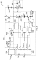
- FIG. 5 is a block diagram 40 of a monitoring circuit MC for measuring the value of a threshold voltage V TH in a Power MOSFET 100 which is coupled to an external device 300, i.e., a load 300, according to embodiments of the present description.
- monitoring circuit MC may be embedded, for instance, in a power actuator, in an electric fuse, or similar.
- the Power MOSFET 100 of Figure 3 is configured to:
- the gate driver 104 is configured to vary the value of a gate-source voltage V GS , i.e., the voltage between the gate terminal G and the source terminal S, of the Power MOSFET 100 in response to the reception of a command C ON/OFF from the controller 102 (previously described and not shown in Figure 5 ).
- the gate driver 104 has a first output terminal that is configured to be coupled to the gate terminal G of the Power MOSFET 100, for instance, through the first switch 402, and a second output terminal that is configured to be coupled to the source terminal S of the Power MOSFET 100.
- the gate driver 104 is configured to set the value of the gate-source voltage V GS to a first value that is higher than the value of the threshold voltage V TH of the Power MOSFET 100 in order to set the state of such Power MOSFET 100 to the conductive ON state.
- the gate driver 104 is configured to set the value of the gate-source voltage V GS to a second value that is lower than the value of the threshold voltage V TH , for instance, to zero, in order to set the state of the Power MOSFET 100 to the non-conductive OFF state.
- the first switch 402 is configured to couple the first output terminal of the gate driver 104 to the gate terminal G of the Power MOSFET 100, such coupling being enabled in response to the reception of a disconnect gate driver signal D GD from a timing block 400, for instance, a microcontroller, a control logic, or other types of processing units, indicating to couple the gate driver 104 to the Power MOSFET 100.
- a disconnect gate driver signal D GD from a timing block 400, for instance, a microcontroller, a control logic, or other types of processing units, indicating to couple the gate driver 104 to the Power MOSFET 100.
- the first switch 402 is further configured to receive a disconnect gate driver signal D GD from the timing block 400 and to change its state, i.e., to open or close, in response to such disconnect gate driver signal D GD .
- disconnect gate driver signal D GD indicates to couple the gate driver 104 to the Power MOSFET 100, such first switch 402 is configured to close.
- the first switch 402 is configured to remain open in response to the disconnect gate driver signal D GD indicating to decouple the gate driver 104 from the Power MOSFET 100.
- the current source 200 for instance, a current generator, is configured to be coupled to the source terminal S of the Power MOSFET 100, for instance, through the third switch 420, and to generate a test current I TEST flowing through the load 300 and/or the source terminal S of the Power MOSFET 100.
- the third switch 420 is configured to couple such current source 200 to the source terminal S of the Power MOSFET 100 and to the load 300, such coupling being enabled in response to the reception of a connect load test signal C LTEST from the timing block 400 indicating to couple the current source 200 to such MOSFET 100 and such load 300.
- the third switch 420 is further configured to receive a connect load test signal C LTEST from the timing block 400 and to change its state, i.e., to open or close, in response to such connect load test signal C LTEST .
- the third switch 420 is configured to remain open in response to the connect load test signal C LTEST indicating to decouple the current source 200 from the Power MOSFET 100 and the load 300.
- the voltage generator 404 is configured to supply a test voltage of value V TEST between the gate terminal G and the source terminal S of the Power MOSFET 100, thus, controlling the gate-source voltage V GS value.
- such voltage generator 404 is configured to be coupled to the second output terminal of the gate driver 104, i.e., to the source terminal S of the Power MOSFET 100, and to the gate terminal G of the Power MOSFET 100, for instance, through the second switch 406.
- Such test voltage of value V TEST supplied by the voltage generator 404 is a voltage that diverges from a nominal value of the threshold voltage NV TH of a chosen amount V GAP , that can be set according to the application considered and to the safety level that is to be respected.
- test voltage V TEST being the value of the test voltage V TEST smaller than the nominal threshold voltage NV TH of a given amount V GAP , when such test voltage V TEST is applied between the gate terminal G and the source terminal S of the Power MOSFET 100 the corresponding MOSFET 100 is expected to remain in a non-conductive OFF state.
- the actual threshold voltage AV TH is shifted from the nominal one NV TH , for instance, because of physical degradations of the gate structure, of an amount equal to or higher than the chosen value V GAP , i.e., so that the actual threshold voltage AV TH is equal to or lower than the voltage V TEST , it may be possible that in response to the application of the test voltage V TEST between the gate terminal G and the source terminal S of the Power MOSFET 100, such MOSFET 100 may shift to a conductive ON state, i.e., a current I DS starts flowing between the drain terminal D and the source terminal S of the Power MOSFET 100.
- the load 300 may be used as a current sensor to check if a current I DS is flowing between the drain terminal D and the source terminal S of the Power MOSFET 100, independently from the circuitry of the load itself and/or from the circuity of a power actuator wherein embodiments of the proposed solutions may be embedded.
- the Power MOSFET 100 may contain a current mirror referred to as FET, therefore, such current mirror may be used as the current sensor itself.
- the test voltage V TEST and, as a consequence, the chosen value V GAP may be fixed.
- the monitoring circuit MC of Figure 5 is configured to raise an alarm if the actual threshold voltage AV TH reaches the test voltage V TEST (i.e., is equal to or lower than the voltage V TEST ).
- Such a condition may be identified by detecting an unexpected variation of the voltage V LOAD on the load 300 in response to the test voltage V TEST being applied to the Power MOSFET 100 and causing a switch of such MOSFET 100 from a non-conductive OFF state to a conductive ON state, i.e., generating a current I DS that flows between the drain terminal D and the source terminal S.
- test voltage V TEST and, as a consequence, the chosen value V GAP may be dynamic.
- the following operations are performed by the monitoring circuit MC of Figure 5 :
- the actual threshold voltage AV TH may be measured since such actual threshold voltage AV TH corresponds to the chosen voltage V TEST .
- such measurement of the actual threshold voltage AV TH may be retrieved if the current flowing in the load 300 is compatible with a measurable currents range of the load 300, wherein such measurable currents range depends on a minimum measurable voltage and on the value of the resistive component R LOAD of the load 300.
- the second switch 406 is configured to couple such voltage generator 404 to the gate terminal G of the Power MOSFET 100, such coupling being enabled in response to the reception of a voltage equality signal V EQ from the timing block 400 indicating to couple the voltage generator 404 to the Power MOSFET 100, in order to set the value of the gate-source voltage V GS to a value substantially equal (i.e., considering a given tolerance range) to the voltage V TEST .
- the second switch 406 is further configured to receive a voltage equality signal V EQ from the timing block 400 and to change its state, i.e., to open or close, in response to such voltage equality signal V EQ .
- the second switch 406 is configured to remain open in response to the voltage equality signal V EQ indicating to decouple the voltage generator 404 from the Power MOSFET 100.
- the timing block 400 is configured to receive at least a test enable signal TE, indicating if a test of the value of the threshold voltage V TH of the Power MOSFET 100 is to be performed using the monitoring circuit MC of Figure 5 , and a test mode signal TM, indicating which test mode in a plurality of test mode is to be used for a current test of the value of the threshold voltage V TH of the Power MOSFET 100 using such monitoring circuit MC of Figure 5 .
- the plurality of test mode may include at least:
- Such first mode may further comprise at least:
- the timing block 400 is further configured to generate a plurality of control signals, such plurality of control signals comprising at least the following signals:
- a sensing block 408 is configured to have a sensing terminal coupled to the source terminal S of the Power MOSFET 100 and to the load 300, and an output terminal coupled to the first sample and hold block 410 and to the second sample and hold block 412. Such sensing block 408 is further configured to:
- the first sample and hold block 410 is configured to receive the sensed value of the voltage V LOAD from the sensing block 408 and the first load voltage sampling signal S VLOAD,T0 from the timing block 400, and, in response to the reception of such first load voltage sampling signal S VLOAD,T0 indicating to sample the received signal, is further configured to sample the received sensed value of the voltage V LOAD and to hold its value for a given time, for instance, a time longer than a selected time period T d , while providing it to a subtracting block 414.
- the second sample and hold block 412 is configured to receive the sensed value of the voltage V LOAD from the sensing block 408 and the second load voltage sampling signal S VLOAD,Td from the timing block 400, and, in response to the reception of such second load voltage sampling signal S VLOAD,TD indicating to sample the received signal, is further configured to sample the received sensed value of the voltage V LOAD and to hold its value for a given time, for instance, a time longer or shorter than the selected time period T d , while providing it to the subtracting block 414.
- the subtracting block 414 is configured to receive sensed value of the voltage V LOAD from both the first sample and hold block 410 and the second sample and hold block 412, to subtract the sensed value received from the second sample and hold block 412 from the sensed value received from the first sample and hold block 410, and to provide the result of such subtraction to a first input terminal of a comparator 418.
- the functions that are performed by the sensing block 408, the first sample and hold block 410, the second sample and hold block 412, and the subtracting block 414 may be performed by a detection unit 408-414 that is configured to:
- such functions that are performed by the sensing block 408, the first sample and hold block 410, the second sample and hold block 412, and the subtracting block 414 may be performed by different real implementations, for instance, such functions may be implemented without using a first and a second sample and hold blocks 410-412.
- the reference voltage generator 416 and the comparator 418 may be coupled to a ground terminal GND for the first test mode and to the voltage of value Vs for the second test mode. Then the voltage variation may be obtained by monitoring the output of the comparator 418, for instance, after a delay T d .
- a reference voltage generator 416 is configured to supply a second input terminal of the comparator 418 with a reference voltage of value V REF .
- such reference voltage value V REF generated by the reference voltage generator 416 may be determined according to the current test mode considered, i.e., according to the current value of the test mode signal TM.
- the comparator 418 for instance, implemented through an operational amplifier, is configured to receive at its first input terminal the result of the subtraction from the subtracting block 414 or the voltage variation provided by the detection unit 408-414 and at its second input terminal the reference voltage V REF from the reference voltage generator 416.
- Such comparator 418 is further configured to compare the voltage values received at its first and second input terminals, and, if the result of such comparison is unsuccessful, the comparator 418 is configured to raise an alarm signal AL VTH , indicating that the corresponding circuit may be at risk of short circuit failures.
- the result of such comparison may be considered as unsuccessful if the output of the comparison does not correspond to a predetermined output condition, such predetermined output condition may depend on the current test mode considered, for instance:
- the reference voltage generator 416 and the comparator 418 may be comprised in the alarm generation unit 416-418 that is configured to:
- the circuit MC for monitoring an actual threshold voltage value AV TH of a MOSFET 100 i.e., the current value of the threshold voltage V TH of the MOSFET 100, comprises:
- control unit 400 is further configured to, according to said received test mode signal TM, select the status of coupling or decoupling of said current source 200 to/from the source terminal S of the MOSFET 100,
- Figure 6 is a time diagram illustrating the behavior of signals in the monitoring circuit MC of Figure 5 according to embodiments of the present description.
- Figure 6 illustrates the behavior of signals received by or generated from the timing block 400.
- the timing block 400 is configured to indicate, for instance, by sending a pulse on the first load voltage sampling signal S VLOAD,T0 or by switching it to a high logic level, to the first sample and hold block 410 to sample the sensed value of the voltage V LOAD before any changes in the operation of the circuit.
- the timing block 400 is configured to modify the operation of the monitoring circuit MC of Figure 5 indicating, for instance, by setting the voltage equality signal V EQ to a high logic level, to couple the voltage generator 404 to the gate terminal G of the Power MOSFET 100, setting the value of the gate-source voltage V GS to a value substantially equal to the voltage V TEST .
- the timing block 400 is further configured to indicate, for instance, by sending a pulse on the second load voltage sampling signal S VLOAD,Td or by switching it to a high logic level, to the second sample and hold block 412 to sample the sensed value of the voltage V LOAD that may have been changed after the setting of the gate-source voltage V GS to the voltage V TEST , thus, the voltage V LOAD is sampled after changes in the operation of the circuit.
- the subtracting block 414 may subtract the sensed voltage V LOAD received from the second sample and hold block 412, i.e., the sensed voltage V LOAD after the setting of the gate-source voltage V GS to the voltage V TEST , from the sensed voltage V LOAD received from the first sample and hold block 410, i.e., before any changes in the operation of the circuit.
- the available test modes in the plurality of test modes are chosen in order to avoid interferences with the operations of a coupled load 300, for instance, an ECU.
- the monitoring circuit MC may advantageously be activated, for instance, by setting the test enable signal TE to a high logic level, only in specific working conditions, for instance, when the coupled load 300 is in an OFF state or in a standby mode, in particular:
- the monitoring circuit MC may be activated when the coupled load 300 is in an OFF state, i.e., there is no current flowing within such load 300, for instance, a case when a power actuator directly activates a load that is resistive and/or capacitive.
- the voltage V LOAD on the load 300 is a very low voltage, for instance, a voltage close to zero, thus, the corresponding gate-source voltage V GS of the Power MOSFET 100 is substantially equal to zero.
- Figure 7 is a time diagram illustrating the behavior of signals in the monitoring circuit MC of Figure 5 when the coupled external device 300, i.e., the coupled load 300, is in an OFF state and may be modeled as a resistive R LOAD load according to embodiments of the present description.
- the connect load test signal C LTEST supplied by the timing block 400 to the third switch 420 is set, for instance, to a low logic level, indicating to such third switch 420 to open in order to decouple the current source 200 from the source terminal S of the Power MOSFET 100. Therefore, the test current I TEST is not flowing within the load 300.
- the timing block 400 is configured to indicate, for instance, by sending a pulse on the first load voltage sampling signal S VLOAD,T0 or by switching it to a high logic level, to the first sample and hold block 410 to sample the sensed value of the voltage V LOAD before any changes in the operation of the monitoring circuit MC, i.e., when the gate-source voltage V GS of the Power MOSFET 100 is substantially equal to zero and the load is in a non-conductive OFF state.
- the timing block 400 is configured to indicate, for instance, by setting the voltage equality signal V EQ to a high logic level, to the second switch 406 that the voltage generator 404 is to be coupled to the gate terminal G of the Power MOSFET 100, to modify the value of the gate-source voltage V GS , setting its value to a value substantially equal to the voltage V TEST .
- the voltage equality signal V EQ may be set to a voltage level equal to the test voltage V TEST supplied by the voltage generator 404 in order to indicate to the second switch 406 to couple the voltage generator 404 to the Power MOSFET 100.
- the Power MOSFET 100 remains in a non-conductive OFF state, thus, there is no current I LOAD flowing within the load 300 and the voltage V LOAD on the load 300 remains of the same value that has been previously sampled by the first sample and hold block 410.
- the sensed value of the voltage V LOAD sampled by the second sample and hold block 412 will be substantially equal to the one sampled by the first sample and hold block 410.
- the result of the subtraction from the subtracting block 414 or the voltage variation provided by the detection unit 408-414 will result in a value that is substantially equal to zero.
- the Power MOSFET 100 may change its state from a non-conductive OFF state to a conductive ON state, since the voltage applied between its gate terminal G and its source terminal S, i.e., the test voltage V TEST , is higher than the actual threshold voltage AV TH value.
- a current I DS starts flowing between the drain terminal D and the source terminal S of the Power MOSFET 100 and, as a consequence, within the load 300, i.e., a resistive load.
- the resistive load 300 which is composed only of a resistive component R LOAD , may be used as a current sensor to check if the Power MOSFET 100 has changed its state from a non-conductive OFF state to a conductive ON state.
- the timing block 400 is further configured to indicate, for instance, by sending a pulse on the second load voltage sampling signal S VLOAD,Td or by switching it to a high logic level, to the second sample and hold block 412 to sample the sensed value of the voltage V LOAD .
- the Power MOSFET 100 may have changed its state from a non-conductive OFF state to a conductive ON state and a variation of both the voltage V LOAD on the load 300 and of the current I LOAD within the load 300 may have been observed.
- the sensed value of the voltage V LOAD sampled by the second sample and hold block 412 is substantially equal to the one sampled by the first sample and hold block 410.
- the subtracting block 414 may subtract the sensed voltage V LOAD received from the second sample and hold block 412, i.e., the voltage V LOAD sensed after such time T d from the setting of the gate-source voltage V GS to the voltage V TEST ,i.e., when such load 300 may have changed its state to a conductive state, from the sensed voltage V LOAD received from the first sample and hold block 410, i.e., the voltage V LOAD sensed before any modification in the operation of the monitoring circuit MC, i.e., with such load 300 in a non-conductive off state, obtaining a value indicative of the voltage variation on the load 300 during such period of time T d .
- such value indicative of the voltage variation on the load 300 indicates a voltage variation between a conductive state of such load 300 and a non-conductive off state of such load 300.
- such value indicative of the voltage variation on the load 300 may indicate if a current I LOAD was flowing within the load 300 during the time period T d .
- the actual threshold voltage AV TH is higher than the test voltage V TEST and a current I LOAD did not flow within such load 300 during such time T d .
- the actual threshold voltage AV TH is equal to or lower than the test voltage V TEST and a current I LOAD flowed within such load 300 during such time T d .
- V REF a reference voltage (as illustrated in Figure 7 ) whose value is:
- the reference voltage V REF may be a voltage referred to a ground terminal GND since the Power MOSFET is initially in a non-conductive OFF state.
- the reference voltage V REF may be illustrated, as in Figures 7 and 8 , with a double arrow between a first level indicating a corresponding ground voltage, i.e., with a value that is substantially zero, and a second level indicating a voltage value that satisfy the two conditions described above for configuring correctly the reference voltage generator.
- a criterion for dimensioning such time T d is described in the following.
- Figure 8 is a time diagram illustrating the behavior of signals in the monitoring circuit MC of Figure 5 when the coupled external device 300 is in an OFF state and may be modeled as a capacitive/resistive load according to embodiments of the present description.
- the Power MOSFET 100 changes its state from a non-conductive OFF state to a conductive ON state, with a consequent variation of both the voltage V LOAD on the load 300 and of the current I LOAD within the load 300.
- the voltage V LOAD on the load 300 slowly variates its value as the capacitive component C LOAD of the load 300 is charged (illustrated in Figure 8 ).
- the load 300 may be used as a current sensor to check if the Power MOSFET 100 has changed its state from a non-conductive OFF state to a conductive ON state, on condition that the time T d used as a delay between the first sampling and the second sampling of the sensed voltage V LOAD is dimensioned in order to allow a complete charging of the capacitive component C LOAD of the load 300 before the second sampling operation.
- the time T d used as a delay between the first sampling and the second sampling of the sensed voltage V LOAD is dimensioned in order to allow the current I LOAD flowing within such coupled load 300 to charge such capacitive component C LOAD .
- the load 300 is not configured to include a capacitive component C LOAD but only a resistive component R LOAD , even if a time T d used as a delay between the first sampling and the second sampling of the sensed voltage V LOAD is still required, such time T d may be much shorter than that of embodiments wherein the load 300 may include a capacitive component C LOAD , as the voltage V LOAD on a load 300 comprising only a resistive component R LOAD varies much faster than on a load 300 comprising also a capacitive component C LOAD .
- the monitoring circuit MC may be activated when the load 300 is in a standby mode, i.e., when there is a supply voltage V FUSE provided to the load 300 but there is no current flowing within such load 300, for instance, a case when an electronic fuse guarantees a supply voltage V FUSE to the load 300 while such load 300 is in a standby mode and no current is flowing through it.
- the load 300 may include a bulk capacitor placed in parallel with an automotive load and a corresponding quiescent current, i.e., a current flowing within an integrated circuit when such circuit is in a quiescent state, for example, in a standby mode, has a very low value such that the load 300 may be modeled with a pure capacitive load, neglecting the resistive component.
- a quiescent current i.e., a current flowing within an integrated circuit when such circuit is in a quiescent state, for example, in a standby mode
- the Power MOSFET 100 or a corresponding device, for instance, an E-Fuse, can be turned off for a short time, i.e., for a time equal to a delay T d , and during such short time a low test current I TEST can be sink from such load 300, for instance, by using a dummy load as the current generator 200. If such test current I TEST is sufficiently low, the capacitive component, for instance, a bulk capacitance, discharging is low enough to avoid an undervoltage condition on such load 300.
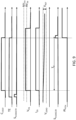
- Figure 9 and Figure 10 are time diagrams illustrating the behavior of signals in the monitoring circuit MC of Figure 5 when the coupled external device 300, modeled as a pure capacitive load, is in an ON state and in a standby mode according to embodiments of the present description.
- Figure 9 illustrates the behavior of signals in the monitoring circuit MC of Figure 5 when coupled to an external device 300, modeled as a pure capacitive load, that is in an ON state and in a standby mode, and the actual value of the threshold voltage AV TH is smaller than or equal to the test voltage V TEST , and, as a consequence, of the nominal value of the threshold voltage NV TH .
- the timing block 400 is configured to indicate, for instance, by sending a pulse on the first load voltage sampling signal S VLOAD,T0 or by switching it to a high logic level, to the first sample and hold block 410 to sample the sensed value of the voltage V LOAD before any changes in the operation of the circuit, i.e., when the gate-source voltage V GS of the Power MOSFET 100 is substantially equal to zero and the load 300 is in a standby mode, i.e., there is a supply voltage V FUSE provided to the load 300 but there is no current flowing within such load 300.
- the connect load test signal C LTEST supplied by the timing block 400 to the third switch 420 is switched, for instance, from a low logic level to a high logic level, indicating to such third switch 420 to close in order to couple the current source 200 to the source terminal S of the Power MOSFET 100.
- the test current I TEST start flowing within the load 300, discharging the capacitive component of such load 300.
- the timing block 400 is configured to indicate, for instance, by setting the voltage equality signal V EQ to a high logic level, to the second switch 406 that the voltage generator 404 is to be coupled to the gate terminal G of the Power MOSFET 100, to modify the value of the gate-source voltage V GS , setting its value to a value substantially equal to the voltage V TEST .
- the voltage equality signal V EQ may be set to a voltage level equal to the test voltage V TEST supplied by the voltage generator 404 in order to indicate to the second switch 406 to couple the voltage generator 404 to the Power MOSFET 100.
- the Power MOSFET 100 changes its state from a non-conductive OFF state to a conductive ON state, as the voltage applied between its gate terminal G and its source terminal S, i.e., the test voltage V TEST , is higher than the actual threshold voltage AV TH value.
- a current I DS starts flowing between the drain terminal D and the source terminal S of the Power MOSFET 100, such current I DS substantially corresponding to the test current I TEST generated by the current source 200.
- the voltage V LOAD on the corresponding load 300 may change of an amount that is smaller than a given threshold, for instance, smaller than a value selected for the reference voltage V REF generated by the reference voltage generator 416.
- V REF generated by the reference voltage generator 416 may be considered as a threshold and used to check if the Power MOSFET 100 has changed its state from a non-conductive OFF state to a conductive ON state.
- the corresponding Power MOSFET 100 is characterized by an actual threshold voltage AV TH value that is smaller than the test voltage V TEST supplied by the voltage generator 404, i.e., is smaller than a selected minimum value and may be at risk of short circuit failures.
- the timing block 400 is further configured to indicate, for instance, by sending a pulse on the second load voltage sampling signal S VLOAD,Td or by switching it to a high logic level, to the second sample and hold block 412 to sample the sensed value of the voltage V LOAD after the setting of the gate-source voltage V GS to the voltage V TEST , thus, when the Power MOSFET 100 has changed its state from a non-conductive OFF state to a conductive ON state and the test current I TEST generated by the current source 200 is flowing within such MOSFET 100.
- the subtracting block 414 may subtract the sensed the voltage V LOAD received from the second sample and hold block 412, i.e., the voltage V LOAD sensed after the Power MOSFET 100 changes its state from a non-conductive OFF state to a conductive ON state, from the sensed the voltage V LOAD received from the first sample and hold block 410, i.e., the voltage V LOAD sensed before any change in the operations of the monitoring circuit MC of Figure 5 , obtaining a value indicative of the voltage variation on the load 300 during the time T d .
- Such value indicative of the voltage variation on the load 300 during the time T d may indicate if a current I LOAD equal to the test current I TEST was flowing within the load 300 during the time T d .
- the voltage V LOAD on the load 300 decreased by an amount that is smaller than such selected threshold during the time T d , thus, a current I LOAD of value equal to the test current I TEST flows within the Power MOSFET 100 and not within such load 300 during such time T d .
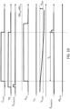
- Figure 10 illustrates the behavior of signals in the monitoring circuit MC of Figure 5 when coupled to an external device 300, modeled as a pure capacitive load , that is in an ON state and in a standby mode, and wherein the actual value of the threshold voltage AV TH is comprised in a range between the test voltage V TEST and the nominal value of the threshold voltage NV TH (for instance, without losing generality for the following description, in Figure 10 the actual value of the threshold voltage AV TH is considered equal to the nominal value of the threshold voltage NV TH ).
- the Power MOSFET 100 do not change its state into a conductive ON state in response to the connect load test signal C LTEST indicating to close the third switch 420, coupling the current source 200 to the source terminal S of the Power MOSFET 100, and the voltage equality signal V EQ indicating to close the second switch 406, coupling the voltage generator 404 to the gate terminal G of the Power MOSFET 100.
- the gate-source voltage V GS of the Power MOSFET 100 is set to the test voltage V TEST but since the actual threshold voltage AV TH is higher than such test voltage V TEST the Power MOSFET 100 remains in a non-conductive OFF state.
- a current I DS is not flowing between the drain terminal D and the source terminal S of the Power MOSFET 100 and the test current I TEST generated by the current source 200 discharge the capacitive component of the load 300, lowering the value of the voltage V LOAD on the load 300.
- the voltage V LOAD on the load 300 decrease over time of an amount that is higher than a given threshold, for instance, higher than the selected value for the reference voltage V REF generated by the reference voltage generator 416.
- the corresponding Power MOSFET 100 is characterized by an actual threshold voltage AV TH value that is higher than the test voltage V TEST supplied by the voltage generator 404, i.e., is higher than the selected minimum value and is not at risk of short circuit failures.
- the value of the voltage variation provided by the subtracting block 414 is higher than the selected threshold, i.e., the reference voltage V REF , as the voltage V LOAD on the load 300 decreased of an amount that is higher than such selected threshold during the time T d , thus, a current I LOAD of value equal to the test current I TEST flowed within such load 300 during such time T d , discharging the capacitive component of such load 300.
- V REF (as illustrated in Figure 9 ) whose value is:
- the alarm signal AL VTH is not set, for instance, remaining to a low logic level (as illustrated in Figure 10 ).
- the reference voltage V REF may be a voltage referred to the voltage Vs since the Power MOSFET is initially in a conductive ON state.
- the reference voltage V REF may be illustrated, as in Figures 9 and 10 , with a double arrow between a first level indicating such voltage Vs and a second level indicating a voltage value that satisfy the two conditions described above for configuring correctly the reference voltage generator.
- I TEST C LOAD ⁇ dV LOAD dT d wherein dV LOAD dT d is the voltage variation over the time period T d provided by the subtracting block 414 or the detection unit 408-414.
- the time T d used as a delay between the first sampling and the second sampling of the sensed voltage V LOAD may be shorter than that of embodiments wherein the load 300 may include both a resistive component and a capacitive component, as in embodiments of Figure 8 .
- the voltage variation measured on the load 300 that may allow detecting an anomaly is much smaller than the one in embodiments of Figure 8 , as the capacitive component is to be partially, and not fully, discharged/charged, thus, needing for a shorter time period T d .
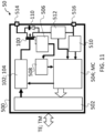
- Figure 11 is a system 50 comprising the monitoring circuit MC of Figure 5 and a temperature variation monitoring unit 506-508 according to embodiments of the present description.
- the threshold voltage V TH of a Power MOSFET 100 decreases in response to increasing temperatures. Therefore, in various embodiments, the test voltage V TEST supplied by the voltage generator 404 is to be compensated for the temperature effects, i.e., in order to maintain a same chosen gap amount V GAP between such test voltage V TEST and the nominal value of the threshold voltage NV TH which changes with temperature values.
- the compensation of the drift of the threshold voltage V TH resulting from a temperature variation is done by using a thermal sensor 506 that is configured to monitor the temperature of the Power MOSFET 100 junction (dashed arrow), and to send the sensed temperature values to a compensation block 508.
- Such compensation block 508 is configured to receive the sensed temperature values from the thermal sensor 506 and to compute as a function of such sensed temperature values a corresponding value for the test voltage V TEST that is to be generated by the voltage generator 404 of a monitoring circuit 504, corresponding to the monitoring circuit MC of Figure 5 .
- the computed value for the test voltage V TEST may be updated dynamically according to the temperature changes of the Power MOSFET 100 in order to keep a gap of constant value V GAP between the nominal threshold voltage NV TH and the test voltage V TEST .
- Such compensation block 508 is further configured to provide such computed value for the test voltage V TEST to the monitoring circuit 504, in particular, to the voltage generator 404.
- the monitoring circuit 504 may further receive current feedback and/or voltage feedback through an ammeter 512 and a voltmeter 510 respectively.
- the monitoring circuit 504 may be coupled to a communication interface 502, for instance, to receive the test enable signal TE and the test mode signal TM from an external unit.
- the thermal sensor 506 and the compensation block 508 may be integrated within the same unit, for instance, within a smart power actuator that comprises a thermal sensor integrated inside the structure of the Power MOSFET.
- the system 50 may be used for automotive applications, for instance, by coupling an upper pin 514 to an automotive power distribution source, for instance, a battery, and a lower pin 516 to a vehicle utility system or to an ECU.
- an automotive power distribution source for instance, a battery
- a lower pin 516 to a vehicle utility system or to an ECU.
- system 50 may be used for automotive applications in contexts of vehicle diagnostic and monitoring systems, multiple and backup power systems, redundant braking systems, redundant electrical power steering system, and/or the like.
- the monitoring circuit MC of Figure 5 may be embedded inside a power actuator or an E-Fuse.
- Solutions as described herein facilitate obtaining monitoring circuits for an early detection of short circuit failures in MOSFETs. This may be achieved by measuring the actual threshold voltage value of a given MOSFET while such MOSFET is coupled with a corresponding load.
- solutions as described herein facilitate achieving the health monitoring of devices, for instance, E-Fuses, through the monitoring of corresponding MOSFETs so as to prevent short circuit failures in such MOSFETs.
- E-Fuses E-Fuses
Landscapes
- Physics & Mathematics (AREA)
- General Physics & Mathematics (AREA)
- Engineering & Computer Science (AREA)
- Microelectronics & Electronic Packaging (AREA)
- Measurement Of Current Or Voltage (AREA)
- Electronic Switches (AREA)
Abstract
- a current source (200), configured to be coupled to a source terminal (S) of the MOSFET (100) and to generate a test current (ITEST),
- a voltage generator (404), configured to be coupled between a gate terminal (G) of the MOSFET (100) and the source terminal (S) of the MOSFET (100), and to generate a test voltage, said test voltage being lower than a nominal threshold voltage value of the MOSFET (100),
- a detection unit (408-414), configured to sample a plurality of voltage value (VLOAD) at the source terminal (S) of the MOSFET (100) during time, to compute as a function of said plurality of voltage value (VLOAD) at least a value of voltage variation over time, in particular over a given time period, of said voltage value (VLOAD) at the source terminal (S) of the MOSFET (100), and to provide said computed at least a value of voltage variation to an alarm generation unit (416-418),
- the alarm generation unit (416-418) being configured to receive said computed voltage variation from the detection unit (408-414), to compare said computed voltage variation with a reference voltage, and to raise an alarm (ALVTH) if the output of said comparison does not correspond to a predetermined output condition, and
- a control unit (400), configured to receive a test mode signal, indicative of an operation mode,
wherein said control unit (400) is further configured to, according to said received test mode signal, select the status of coupling or decoupling of said current source (200) to/from the source terminal (S) of the MOSFET (100),
- determine the value of said reference voltage,
- set said output condition of said comparison, and
- signal to the detection unit (408-414) to perform a plurality of said sampling operation.
Description
- The description relates to monitoring circuits.
- One or more embodiments can be applied to circuits for monitoring a health state of transistors.
- Health monitoring of electronic components is the prognosis of potential failures of such components and consists in measuring the deviation of electrical parameters that can be correlated with the physical degradation of such components.
- Health monitoring is of great importance as electronic components are widely used in most systems and their failures may lead to breakdowns and/or shutdowns of such systems, so preventing such failures may increase the robustness and reliability of systems.
- Specifically, health monitoring is of relevance in the automotive field wherein preventing hazards may increase passenger safety.
- In fact, ISO26262, which is the actual international standard considered for the functional safety of electrical and/or electronic systems that are installed in serial production road vehicles, defines a minimum requirement for safety which is measured using the Automotive Safety Integrity Level (ASIL) that is a safety level determined through hazard analysis and risk assessment.
- Therefore, failures prediction and health monitoring of vehicle's electrical components may increase the ASIL safety level of a vehicle, allowing preemptive maintenance or replacement of electronic components considered at risk.
- To satisfy ISO26262 requirements, safety critical environments such as automotive power distribution environments may use E-Fuses ("Electronic Fuses") with a high ASIL safety level. Such E-Fuses are integrated power path protection devices used to limit circuit currents and/or voltages to safe levels during fault conditions.
- Usually, such E-Fuses may perform an inrush current control using a Power MOSFET. In certain failure conditions, such Power MOSFET may be affected by short circuit failures, i.e., failures wherein the Power MOSFET cannot be controlled through its gate to be turned off, lowering the reliability of E-Fuses and, consequently, leading to a safety-critical situation.
- Such short circuit failures in Power MOSFETs may be generated by physical degradations of the gate structure, such as:
- a high leakage in the oxide of the gate, and/or
- a presence of charges trapped in the oxide of the gate.
- In particular, this last condition may result in a reduction of the threshold voltage of a Power MOSFET, such threshold voltage corresponding to the voltage needed for switching the state of such Power MOSFET from a non-conductive state ("OFF") to a conductive state ("ON").
- Such reduction may continue until the Power MOSFET, and consequently the corresponding device, i.e., the corresponding E-Fuse, remains normally in a conductive ON state, for instance, if the value of the threshold voltage of the Power MOSFET decreases to zero or to a negative value so that such Power MOSFET cannot be controlled through its gate to be turned off, i.e., to be switched to a non-conductive state.
- For example,
Figure 1 illustrates anE-Fuse structure 10 showing the effects of the physical degradation of aPower MOSFET 100. - In
Figure 1 gate capacitance CDG, i.e., between a drain terminal D and a gate terminal G of thePower MOSFET 100, and CGS, i.e., between the gate terminal G and a source terminal S of thePower MOSFET 100, of thePower MOSFET 100 are represented as adrain-gate capacitor 106 of value equal to CDG and a gate-source capacitor 108 of value equal to CGS respectively. - A
controller 102 is configured to send to agate driver 104 an ON command Corr or an OFF command COFF, in order to set the state of thePower MOSFET 100 to an ON state, i.e., a conductive state, or to an OFF state, i.e., a non-conductive state, respectively. - The
gate driver 104 is configured to vary the value of a gate-source voltage VGS between the gate terminal G and the source terminal S of thePower MOSFET 100 in response to the reception of a command from thecontroller 102. - In particular, in response to the ON command Corr, the
gate driver 104 is configured to set the value of the gate-source voltage VGS to a first value that is higher than a threshold voltage VTH of thePower MOSFET 100 in order to set the state ofsuch Power MOSFET 100 to the conductive ON state. - Conversely, in response to the OFF command COFF, the
gate driver 104 is configured to set the value of the gate-source voltage VGS to a second value that is lower than such threshold voltage VTH of thePower MOSFET 100, for instance, to zero, in order to set the state of thePower MOSFET 100 to the non-conductive OFF state. - A
blocking diode 110 is coupled between the source S and the drain D of thePower MOSFET 100 to protect thePower MOSFET 100 against reverse polarity connections. - In
Figure 1 , thecontroller 102 is configured to send the OFF command Corr to thegate driver 104 that, in response to the reception of such OFF command COFF, is configured to set the value of the gate-source voltage VGS to the second value, i.e., to a value lower than the threshold voltage VTH of thePower MOSFET 100, for instance, to zero. - In such a case, if the physical structure of the gate G of the
Power MOSFET 100 is degraded, for instance, resulting in a relevant reduction of the value of the threshold voltage VTH, for instance, if the current value of the threshold voltage VTH is a negative value, both thePower MOSFET 100 and thecorresponding E-Fuse 10 remain in a conductive ON state even after the reception of an OFF command Corr, thus, a current IDS flows between the drain terminal D and the source terminal S of thePower MOSFET 100 even after the reception of such OFF command COFF. - Therefore, the
E-Fuse 10 remains in a conductive ON state even if thecontroller 102 has sent a command for requesting a switch of such E-Fuse to a non-conductive OFF state, thus, generating a short circuit failure characterized by an uncontrolled conduction. - Such short circuit failures strongly compromise safety requirements imposed by ISO26262, since the
Power MOSFET 100 and the corresponding device, i.e., thecorresponding E-Fuse 10, cannot be controlled and switched off if required, i.e.,such E-Fuse 10 with acorresponding Power MOSFET 100 failed in short circuit cannot limit currents and/or voltages to safe levels when required. - In fact, in an
E-Fuse 10 with acorresponding Power MOSFET 100 failed in short circuit, the current IDS flowing between the drain terminal D and the source terminal S of thePower MOSFET 100 cannot be interrupted, and, consequently, a circuit to be protected coupled to the drain terminal D and/or to the source terminal S ofsuch Power MOSFET 100 cannot be interrupted, i.e., its over-currents and/or over-voltages cannot be limited, thus, the protection fails. - In addition, the uncontrolled ON state of a
Power MOSFET 100 may generate high power dissipation, resulting in high temperatures, for instance, rising the temperature of an ECU ("Electronic Control Unit") wherein acorresponding E-Fuse 10 with aPower MOSFET 100 failed in short circuit is installed, leading to fire hazards. - Solutions that facilitate the health monitoring of such devices to prevent short circuit failures would be beneficial in order to have an early prognosis on the degradation of such devices and to prevent potential failures resulting in uncontrolled conduction.
- An object of one or more embodiments is to contribute in providing solutions that facilitate the health monitoring of MOSFETs, preventing short circuit failures in order to have an early prognosis on the degradation of both such MOSFETs and corresponding devices, for instance, E-Fuses, and to prevent potential failures resulting in uncontrolled conduction.
- According to one or more embodiments, that object is achieved via a circuit having the features set forth in the claims that follow.
- One or more embodiments concern a corresponding method.
- The claims are an integral part of the technical teaching provided in respect of the embodiments.
- Solutions as described herein include a circuit for monitoring an actual threshold voltage value of a Power MOSFET comprising:
- a current source, configured to be coupled to a source terminal of the Power MOSFET and to generate a test current,
- a voltage generator, configured to be coupled between a gate terminal of the Power MOSFET and the source terminal of the Power MOSFET, and to generate a test voltage, such test voltage being lower than a nominal threshold voltage value of the Power MOSFET,
- a detection unit, configured to sample a plurality of voltage value at the source terminal of the Power MOSFET during time to compute as a function of such plurality of voltage value at least a value of voltage variation over time, in particular over a given time period, of such voltage value at the source terminal of the Power MOSFET, and to provide such computed at least a value of voltage variation to an alarm generation unit,
- the alarm generation unit being configured to receive such computed voltage variation from the detection unit, to compare such computed voltage variation with a reference voltage, and to raise an alarm if the output of such comparison does not correspond to a predetermined output condition, and
- a control unit, configured to receive a test mode signal, indicative of an operation mode,
- determine the value of such reference voltage,
- set such output condition of such comparison, and
- signal to the detection unit to perform a plurality of such sampling operation.
- In various embodiments, if such test mode signal indicates a first test mode such control unit is configured to:
- decouple such current source from the source terminal of the Power MOSFET,
- determine the value of such reference voltage so that such reference voltage is a positive voltage smaller than any possible value of such computed voltage variation obtained when the value of the actual threshold voltage is equal to or lower than the test voltage, and
- set as such predetermined output condition a result of the comparison between such computed voltage variation and such reference voltage indicating that such computed voltage variation is higher than such reference voltage.
- couple such current source to the source terminal of the Power MOSFET,
- determine the value of such reference voltage so that such reference voltage is higher than any possible value of such computed voltage variation obtained when the value of the actual threshold voltage is equal to or lower than the test voltage and smaller than any possible value of such computed voltage variation obtained when the value of the actual threshold voltage is higher than the test voltage, and
- set as such predetermined output condition a result of the comparison between such computed voltage variation and such reference voltage indicating that such computed voltage variation is smaller than such reference voltage.
- In various embodiments, such test mode signal is configured to indicate a first submode of such first test mode and a second submode of such first mode, wherein in the first submode mode such given time period is shorter than the period in the second mode.
- In various embodiments, such circuit is coupled to an external load through the source terminal of the Power MOSFET, and
the test mode signal selects an operation mode in a set of available operation modes, such set of available operation modes comprising at least: - such first mode, selected when the coupled external load is in an off state such first mode comprising such first submode corresponding to a resistive load and such second submode corresponding to a load comprising both a capacitive component and a resistive component, and
- such second mode, selected when the coupled external load is in an on state, in a standby mode, and the load corresponds to a capacitive load.
- In various embodiments, such MOSFET is a Power MOSFET.
- In various embodiments, such plurality of voltage value comprises a first voltage value and a second voltage value, such first voltage value being retrieved at the beginning of the given time period while such second voltage value being retrieved at the end of the given time period, and
such compute operation to obtain the voltage variation as a function of such plurality of voltage value comprises subtracting such second voltage value from such first voltage value. - In various embodiments, such detection unit comprises:
- a sensing unit, configured to sense voltage values at the source terminal of the Power MOSFET and to forward such sensed voltage values to a first sample and hold block and to a second sample and hold block,
- the first sample and hold block, configured to sample such first voltage value in response to the reception of a signal from the control unit indicating to perform a first of such sampling operation, to hold such first voltage value for an amount of time larger than such given time period, and to provide such first voltage value to a subtracting block,
- the second sample and hold block, configured to sample such second voltage value in response to the reception of a signal from the control unit indicating to perform a second of such sampling operation, to hold such second voltage value, and to provide such second voltage value to the subtracting block,
- the subtracting block, configured to receive the first voltage value from the first sample and hold block and the second voltage value from the second sample and hold block, to perform such subtracting of such second voltage value from such first voltage value obtaining such voltage variation, and to provide such voltage variation to the alarm generation unit.
- In various embodiments, such alarm generation unit comprises:
- a reference voltage generator, configured to provide a comparator block with such reference voltage, and
- the comparator block, configured to receive such computed voltage variation from the detection unit and such reference voltage from the reference voltage generator, to compare such computed voltage variation with such reference voltage, and to raise an alarm in response to an unsuccessful comparison operation.
- In various embodiments, such circuit further comprises:
- a first switch, configured to couple or decouple such current source to the source terminal of the Power MOSFET in response to the reception of a signal from the control unit issued as a function of such test mode signal.
- In various embodiments, such circuit further comprises an additional switch configured to decouple a gate driver from the gate terminal of the Power MOSFET in response to the reception of a signal from the control unit indicating to start the monitoring of such actual threshold voltage value, and to couple the gate driver to the gate terminal of the Power MOSFET in response to the reception of a signal from the control unit indicating to end the monitoring of such actual threshold voltage value.
- In various embodiments, such test voltage is fixed, or such test voltage is dynamic and such control unit is further configured to:
- select an initial value for such test voltage,
- start the monitoring of such actual threshold voltage value,
- if the alarm generation unit do not raise any alarm before the end of the monitoring of such actual threshold voltage value, increase the value of such test voltage of a given step and perform again the steps from the starting of the monitoring, and
- if the alarm generation unit raises an alarm before the end of the monitoring of such actual threshold voltage value, identify the current value of the test voltage as the value of the actual threshold voltage value.
- In various embodiments, such circuit is further coupled with a temperature monitoring unit, such temperature monitoring unit being configured to:
- monitor a temperature of the Power MOSFET to sense at least one temperature value, and
- compute a value for such test voltage as a function of such at least one sensed temperature value, and
- provide such value for such test voltage to the circuit to generate a test voltage of such value through the voltage generator.
- In various embodiments such circuit comprises a further switch, configured to couple or decouple such voltage generator to the gate terminal of the Power MOSFET in response to the reception of a signal from the control unit issued as a function of such test mode signal, and in such first and second mode such voltage generator is maintained coupled from the gate terminal of the Power MOSFET.
- In various embodiments, such first and second mode such voltage generator is decoupled from the gate terminal of the Power MOSFET if a test enable signal mode is not set.
- Solutions as described herein facilitate achieving the health monitoring of devices, for instance, E-Fuses, through the monitoring of corresponding MOSFETs so as to prevent short circuit failures in such MOSFETs. In this way, it may be possible to have an early prognosis on the degradation of both such MOSFETs and corresponding devices, i.e., E-Fuses, and to prevent potential failures resulting in uncontrolled conduction.
- One or more embodiments will now be described, by way of example only, with reference to the annexed figures, wherein:
-
Figure 1 , as already described, illustrates an E-Fuse structure showing the effects of the physical degradation of a Power MOSFET; -
Figure 2 illustrates a solution for measuring the value of the threshold voltage in a Power MOSFET; -
Figure 3 illustrates the solution ofFigure 2 for measuring the value of the threshold voltage in a Power MOSFET which is coupled to an external device; -
Figure 4 is a time diagram illustrating the behavior of signals in the solution ofFigure 3 ; -
Figure 5 is a block diagram of a monitoring circuit for measuring the value of the threshold voltage in a Power MOSFET which is coupled to an external device according to embodiments of the present description; -
Figure 6 is a time diagram illustrating the behavior of signals in the circuit ofFigure 5 according to embodiments of the present description; -
Figure 7 is a time diagram illustrating the behavior of signals in the circuit ofFigure 5 when the coupled external device is off and may be modeled as a resistive load according to embodiments of the present description; -
Figure 8 is a time diagram illustrating the behavior of signals in the circuit ofFigure 5 when the coupled external device is off and may be modeled as a capacitive/resistive load according to embodiments of the present description; -
Figure 9 andFigure 10 are time diagrams illustrating the behavior of signals in the circuit ofFigure 5 when the coupled external device is on, in a standby mode, and may be modeled as a pure capacitive load according to embodiments of the present description; and -
Figure 11 is a system comprising the circuit ofFigure 5 and a temperature variation monitoring unit according to embodiments of the present description. - Corresponding numerals and symbols in the different figures generally refer to corresponding parts unless otherwise indicated.
- The figures are drawn to clearly illustrate the relevant aspects of the embodiments and are not necessarily drawn to scale.
- The edges of features drawn in the figures do not necessarily indicate the termination of the extent of the feature.
- In the ensuing description one or more specific details are illustrated, aimed at providing an in-depth understanding of examples of embodiments of this description. The embodiments may be obtained without one or more of the specific details, or with other methods, components, materials, etc. In other cases, known structures, materials, or operations are not illustrated or described in detail so that certain aspects of embodiments will not be obscured.
- Reference to "an embodiment" or "one embodiment" in the framework of the present description is intended to indicate that a particular configuration, structure, or characteristic described in relation to the embodiment is comprised in at least one embodiment. Hence, phrases such as "in an embodiment" or "in one embodiment" that may be present in one or more points of the present description do not necessarily refer to one and the same embodiment.
- Moreover, particular configurations, structures, or characteristics may be combined in any adequate way in one or more embodiments.
- The headings/references used herein are provided merely for convenience and hence do not define the extent of protection or the scope of the embodiments.
- For simplicity and ease of explanation, throughout this description, and unless the context indicates otherwise, like parts or elements are indicated in the various figures with like reference signs, and a corresponding description will not be repeated for each and every figure.
- In particular, in the following figures, parts, elements and/or components which have already been described with reference to
Figure 1 are denoted by the same references previously used in such figure, therefore, the description of such previously described elements will not be repeated in the following in order not to overburden the present detailed description. - As previously described, it would be beneficial to find solutions that facilitate the health monitoring of MOSFETs, preventing short circuit failures in order to have an early prognosis on the degradation of both such MOSFETs and corresponding devices, i.e., E-Fuses, and to prevent potential failures resulting in uncontrolled conduction.
- According to embodiments of the present disclosure, a diagnostic as explained above, i.e., the health monitoring of MOSFETs and corresponding devices, may be done by monitoring the value of a threshold voltage VTH of a
Power MOSFET 100 whilesuch Power MOSFET 100 is coupled to a given circuit to be protected, i.e., while it is coupled to a given load. - It is noted that even if the following description is mainly focused on solutions using a Power MOSFET, for instance, an N-channel Power MOSFET or a P-channel Power MISFET, solutions as described herein may also be implemented considering GaN transistors or SiC Power MOSFET.
- It is to be noted that even if the following description is mainly focused on the application of proposed solutions in the automotive sector, solutions as described herein may be used also in other application contexts wherein it is needed to measure and/or monitor a threshold voltage of a Power MOSFET with a coupled load, for instance, a resistive and/or capacitive load.
- In many application contexts, standard threshold voltage VTH measurements cannot be used, for instance, as an E-Fuse 10, i.e., a corresponding MOSFET, may be always coupled to a resistive and/or capacitive load, i.e., to a circuit to be protected. In addition, such an E-Fuse 10 may be configured to have the
corresponding Power MOSFET 100 set by default to a conductive ON state (such Power MOSFET 100 may switch to a non-conductive OFF state only in case of over-currents and/or over-voltages detected in such circuit to be protected), so, in most cases, threshold voltage VTH measurements should be performed during the conductive ON state ofsuch Power MOSFET 100. -
Figure 2 illustrates asolution 20 for measuring the value of a threshold voltage VTH in aPower MOSFET 100. - The
Power MOSFET 100 ofFigure 2 is configured to: - have coupled to its drain terminal D a
voltage supply 202, configured to supply thePower MOSFET 100 with a voltage of value Vs, and aswitch 204 configured to be in a closed state; - have coupled to its gate terminal G the
closed switch 204, therefore, both the drain terminal D and the gate terminal G are set to the same voltage level; and - have coupled to its source terminal S a
current source 200, for instance, a current generator, configured to generate a test current of value ITEST, for instance, whose value is the minimum value allowing to switch the state of thePower MOSFET 100 from a non-conductive OFF state to a conductive ON state, i.e., the minimum value allowing to set the gate-source voltage VGS, i.e., the voltage between the gate terminal G and the source terminal S of thePower MOSFET 100, to the value of the current threshold voltage VTH of thePower MOSFET 100. - As illustrated in
Figure 2 , with such astructure 20 the drain-source voltage VDS, i.e., the voltage between the drain terminal D and the source terminal S, is equal to the gate-source voltage VGS, i.e., the voltage between the gate terminal G and the source terminal S, as both the drain terminal D and the gate terminal G are at the same voltage level Vs. - Therefore, in the conditions of
Figure 2 , the drain-source voltage VDS is equal to the gate-source voltage VGS, and both of these voltages are equal to the value of the threshold voltage VTH of thePower MOSFET 100. - Hence, the value of the threshold voltage VTH of the
Power MOSFET 100 may be evaluated as a function of the value of the test current ITEST generated by thecurrent source 200. - Nevertheless, such a
solution 20 cannot be used when a load is coupled to the source terminal S of thePower MOSFET 100. - To this regard,
Figure 3 illustrates thesolution 20 ofFigure 2 for measuring the value of the threshold voltage VTH in aPower MOSFET 100 as coupled to anexternal device 300, i.e., represented by any capacitive load CLOAD, e.g., a load capacitor, and/or resistive load RLOAD, e.g., a load resistor. - It is noted that, although
Figure 3 shows aload 300 comprising a resistive load RLOAD and capacitive load CLOAD,such load 300 may present only a substantial resistive behaviour, i.e., may correspond to or may be modeled with only the resistive load component RLOAD, only capacitive, i.e., may correspond to or be modeled with only the capacitive load component CLOAD, or both resistive component RLOAD and capacitive component CLOAD. - As exemplified in
Figure 3 , when aload 300, for instance, an ECU, is coupled to the source terminal S of thePower MOSFET 100, the value of the test current ITEST generated by thecurrent source 200 cannot be defined and set to a chosen value as its value is influenced by the givenload 300, i.e., by the voltage of the source terminal S that is determined by the voltage VLOAD on theload 300, which may also be a variable voltage. - For example, this may be the case of an automotive environment wherein the
load 300 may represent an ECU, i.e., an Electronic Control Unit, that may be modeled as a both resistive load RLOAD and capacitive (i.e., wherein the capacitor may be a bulk capacitor with a value of about 1 mF) CLOAD load. - Considering the structure illustrated in
Figure 3 , it is noted that the threshold voltage VTH may be measured if theload 300 comprises only a capacitive component CLOAD, for instance, if theload 300 is an ECU in a standby mode Sb modeled as a capacitor CLOAD. In such a case, a measurement of the value of the threshold voltage VTH may be done by closing theswitch 204 and waiting for a charging time CTCLOAD, i.e., until the capacitor CLOAD is charged by the selected test current ITEST. - A drawback is that the capacitive component CLOAD delays for a charging time CCLOAD, i.e., for a time equal to

- For instance, if the capacitive load CLOAD is about 1 mF, the test current ITEST is about 1 mA, and the threshold voltage VTH is about 1.5 V, the charging time CTCLOAD is about 1.5 s, which is not negligible.
-
Figure 4 is a time diagram illustrating the behavior of signals in thesolution 30 ofFigure 3 . - A current signal IRLOAD indicates the current flowing within the resistive component RLOAD of the
load 300. - When the current signal IRLOAD value is zero, for instance, when a corresponding ECU enters in a standby mode Sb, the only remaining component of the
load 300 is the capacitive component CLOAD, therefore, the threshold voltage VTH may be measured. - In response to the value of the current signal IRLOAD reaching zero, a switch control signal SON/OFF commutes, for instance, from a low logic level to a high logic level, in order to command the closure of the
switch 204, and, in response to the closure ofsuch switch 204, the test current ITEST starts flowing in the capacitive component CLOAD of theload 300, charging such capacitive component CLOAD until the voltage VDS remains substantially stable to the threshold voltage VTH value, i.e., after the charging time TCCLOAD. - Solutions that simplify and increase the precision of the monitoring of threshold voltages VTH in transistors, allowing such monitoring even when loads are coupled therewith, would be beneficial in order to have an early prognosis of degradation of devices and to prevent potential failure resulting in uncontrolled conduction.
-
Figure 5 is a block diagram 40 of a monitoring circuit MC for measuring the value of a threshold voltage VTH in aPower MOSFET 100 which is coupled to anexternal device 300, i.e., aload 300, according to embodiments of the present description. - It is noted that such monitoring circuit MC may be embedded, for instance, in a power actuator, in an electric fuse, or similar.
- The
Power MOSFET 100 ofFigure 3 is configured to: - have coupled to its drain terminal D a
voltage supply 202, configured to supply thePower MOSFET 100 with a voltage of value Vs; - have coupled to its gate terminal G a
first switch 402, configured to couplesuch MOSFET 100 to a first output terminal of agate driver 104, and asecond switch 406, configured to couplesuch MOSFET 100 to avoltage generator 404; and - have coupled to its source terminal S a second output terminal of
such gate driver 104, athird switch 420, configured to couplesuch MOSFET 100 to acurrent source 200, and anexternal load 300, that may be of the same types as already described inFigure 3 . - The
gate driver 104 is configured to vary the value of a gate-source voltage VGS, i.e., the voltage between the gate terminal G and the source terminal S, of thePower MOSFET 100 in response to the reception of a command CON/OFF from the controller 102 (previously described and not shown inFigure 5 ). - To this purpose, the
gate driver 104 has a first output terminal that is configured to be coupled to the gate terminal G of thePower MOSFET 100, for instance, through thefirst switch 402, and a second output terminal that is configured to be coupled to the source terminal S of thePower MOSFET 100. - Therefore, in response to the ON command Corr, the
gate driver 104 is configured to set the value of the gate-source voltage VGS to a first value that is higher than the value of the threshold voltage VTH of thePower MOSFET 100 in order to set the state ofsuch Power MOSFET 100 to the conductive ON state. - Conversely, in response to the OFF command COFF, the
gate driver 104 is configured to set the value of the gate-source voltage VGS to a second value that is lower than the value of the threshold voltage VTH, for instance, to zero, in order to set the state of thePower MOSFET 100 to the non-conductive OFF state. - The
first switch 402 is configured to couple the first output terminal of thegate driver 104 to the gate terminal G of thePower MOSFET 100, such coupling being enabled in response to the reception of a disconnect gate driver signal DGD from atiming block 400, for instance, a microcontroller, a control logic, or other types of processing units, indicating to couple thegate driver 104 to thePower MOSFET 100. - In fact, the
first switch 402 is further configured to receive a disconnect gate driver signal DGD from thetiming block 400 and to change its state, i.e., to open or close, in response to such disconnect gate driver signal DGD. - Therefore, if the disconnect gate driver signal DGD indicates to couple the
gate driver 104 to thePower MOSFET 100, suchfirst switch 402 is configured to close. - Conversely, the
first switch 402 is configured to remain open in response to the disconnect gate driver signal DGD indicating to decouple thegate driver 104 from thePower MOSFET 100. - The
current source 200, for instance, a current generator, is configured to be coupled to the source terminal S of thePower MOSFET 100, for instance, through thethird switch 420, and to generate a test current ITEST flowing through theload 300 and/or the source terminal S of thePower MOSFET 100. - The
third switch 420 is configured to couple suchcurrent source 200 to the source terminal S of thePower MOSFET 100 and to theload 300, such coupling being enabled in response to the reception of a connect load test signal CLTEST from thetiming block 400 indicating to couple thecurrent source 200 tosuch MOSFET 100 andsuch load 300. - In fact, the
third switch 420 is further configured to receive a connect load test signal CLTEST from thetiming block 400 and to change its state, i.e., to open or close, in response to such connect load test signal CLTEST. - Therefore, if the connect load test signal CLTEST indicates to couple the
current source 200 to thePower MOSFET 100 and to theload 300, suchthird switch 420 is configured to close. - Conversely, the
third switch 420 is configured to remain open in response to the connect load test signal CLTEST indicating to decouple thecurrent source 200 from thePower MOSFET 100 and theload 300. - The
voltage generator 404 is configured to supply a test voltage of value VTEST between the gate terminal G and the source terminal S of thePower MOSFET 100, thus, controlling the gate-source voltage VGS value. - To this purpose,
such voltage generator 404 is configured to be coupled to the second output terminal of thegate driver 104, i.e., to the source terminal S of thePower MOSFET 100, and to the gate terminal G of thePower MOSFET 100, for instance, through thesecond switch 406. - Such test voltage of value VTEST supplied by the
voltage generator 404 is a voltage that diverges from a nominal value of the threshold voltage NVTH of a chosen amount VGAP, that can be set according to the application considered and to the safety level that is to be respected. - Therefore, being the value of the test voltage VTEST smaller than the nominal threshold voltage NVTH of a given amount VGAP, when such test voltage VTEST is applied between the gate terminal G and the source terminal S of the
Power MOSFET 100 the correspondingMOSFET 100 is expected to remain in a non-conductive OFF state. - It is noted that if the actual threshold voltage AVTH is shifted from the nominal one NVTH, for instance, because of physical degradations of the gate structure, of an amount equal to or higher than the chosen value VGAP, i.e., so that the actual threshold voltage AVTH is equal to or lower than the voltage VTEST, it may be possible that in response to the application of the test voltage VTEST between the gate terminal G and the source terminal S of the
Power MOSFET 100,such MOSFET 100 may shift to a conductive ON state, i.e., a current IDS starts flowing between the drain terminal D and the source terminal S of thePower MOSFET 100. - In response to the current IDS starting flowing between the drain terminal D and the source terminal S of the
Power MOSFET 100, a variation of the voltage VLOAD on theload 300 may be observed. - Therefore, the
load 300 may be used as a current sensor to check if a current IDS is flowing between the drain terminal D and the source terminal S of thePower MOSFET 100, independently from the circuitry of the load itself and/or from the circuity of a power actuator wherein embodiments of the proposed solutions may be embedded. - It may be noted that, generally, the
Power MOSFET 100 may contain a current mirror referred to as FET, therefore, such current mirror may be used as the current sensor itself. - Nevertheless, using such current mirror as current sensor may not be reliable since a drift in the threshold voltage VTH may change the current ratio between a current IDS flowing between the drain terminal D and the source terminal S of the
Power MOSFET 100 and a current flowing in such current mirror, making a sensed current obtained using such current mirror internal tosuch MOSFET 100 unreliable. - In various embodiments, the test voltage VTEST and, as a consequence, the chosen value VGAP, may be fixed. In such cases, the monitoring circuit MC of
Figure 5 is configured to raise an alarm if the actual threshold voltage AVTH reaches the test voltage VTEST (i.e., is equal to or lower than the voltage VTEST). Such a condition may be identified by detecting an unexpected variation of the voltage VLOAD on theload 300 in response to the test voltage VTEST being applied to thePower MOSFET 100 and causing a switch ofsuch MOSFET 100 from a non-conductive OFF state to a conductive ON state, i.e., generating a current IDS that flows between the drain terminal D and the source terminal S. - In various embodiments, the test voltage VTEST and, as a consequence, the chosen value VGAP, may be dynamic. In such cases, the following operations are performed by the monitoring circuit MC of
Figure 5 : - set. the test voltage VTEST and the value VGAP to initial values;
- test the state of the
Power MOSFET 100, i.e., conductive ON state or non-conductive OFF state, for instance, by using theload 300 as current sensor; - if the
Power MOSFET 100 is in a non-conductive OFF state, for example, if a current flowing in theload 300 is not detected, increase of a given step the value of the test voltage VTEST and decrease of the same given step the value VGAP, and return again to the testing step; and - if the
Power MOSFET 100 is in a conductive ON state, for instance, if a current flowing in theload 300 is detected with a corresponding variation of the voltage VLOAD on theload 300, the value of the test voltage VTEST corresponds to the actual threshold voltage AVTH. - Therefore, in embodiments with a dynamic test voltage VTEST the actual threshold voltage AVTH may be measured since such actual threshold voltage AVTH corresponds to the chosen voltage VTEST.
- It is noted that such measurement of the actual threshold voltage AVTH may be retrieved if the current flowing in the
load 300 is compatible with a measurable currents range of theload 300, wherein such measurable currents range depends on a minimum measurable voltage and on the value of the resistive component RLOAD of theload 300. - The
second switch 406 is configured to couplesuch voltage generator 404 to the gate terminal G of thePower MOSFET 100, such coupling being enabled in response to the reception of a voltage equality signal VEQ from thetiming block 400 indicating to couple thevoltage generator 404 to thePower MOSFET 100, in order to set the value of the gate-source voltage VGS to a value substantially equal (i.e., considering a given tolerance range) to the voltage VTEST. - In fact, the
second switch 406 is further configured to receive a voltage equality signal VEQ from thetiming block 400 and to change its state, i.e., to open or close, in response to such voltage equality signal VEQ. - Therefore, if the voltage equality signal VEQ indicates to couple the
voltage generator 404 to thePower MOSFET 100, suchsecond switch 406 is configured to close. - Conversely, the
second switch 406 is configured to remain open in response to the voltage equality signal VEQ indicating to decouple thevoltage generator 404 from thePower MOSFET 100. - The
timing block 400 is configured to receive at least a test enable signal TE, indicating if a test of the value of the threshold voltage VTH of thePower MOSFET 100 is to be performed using the monitoring circuit MC ofFigure 5 , and a test mode signal TM, indicating which test mode in a plurality of test mode is to be used for a current test of the value of the threshold voltage VTH of thePower MOSFET 100 using such monitoring circuit MC ofFigure 5 . - For instance, the plurality of test mode may include at least:
- a first mode wherein the coupled external device is considered in an OFF state; and
- a second mode wherein the coupled external device is considered in an ON state, in a standby mode, and the
load 300 may correspond to or may be modeled as a pure capacitive load CLOAD. - Such first mode may further comprise at least:
- a first submode wherein the coupled external device corresponds to or may be modeled as a resistive load RLOAD; and
- a second submode wherein the coupled external device corresponds to or may be modeled as a
load 300 comprising both a capacitive component CLOAD and a resistive component RLOAD. - As a function of such test enable signal TE and such test mode signal TM, the
timing block 400 is further configured to generate a plurality of control signals, such plurality of control signals comprising at least the following signals: - the disconnect gate driver signal DGD, indicating to the
first switch 402 whether thegate driver 104 is to be coupled to or decoupled from the gate terminal G of thePower MOSFET 100; - the voltage equality signal VEQ, indicating to the
second switch 406 whether thevoltage generator 404 is to be coupled to or decoupled from the gate terminal G of thePower MOSFET 100; - the connect load test signal CLTEST, indicating to the
third switch 420 whether thecurrent source 200 is to be coupled to or decoupled from the source terminal S of thePower MOSFET 100; - a first load voltage sampling signal SVLOAD,T0, indicating to a first sample and hold ("S&H") block 410 whether to sample or not a received signal; and
- a second load voltage sampling signal SVLOAD,Td, indicating to a second sample and hold ("S&H") block 412 whether to sample or not a received signal.
- A
sensing block 408 is configured to have a sensing terminal coupled to the source terminal S of thePower MOSFET 100 and to theload 300, and an output terminal coupled to the first sample and holdblock 410 and to the second sample and holdblock 412.Such sensing block 408 is further configured to: - sense, through its sensing terminal, the value of the voltage at the source terminal S of the
Power MOSFET 100 and theload 300, i.e., the value of the voltage VLOAD, in order to monitor its variations, and - forward, through its output terminal, a sensed value of the voltage VLOAD to the first sample and hold
block 410 and to the second sample and holdblock 412. - The first sample and hold
block 410 is configured to receive the sensed value of the voltage VLOAD from thesensing block 408 and the first load voltage sampling signal SVLOAD,T0 from thetiming block 400, and, in response to the reception of such first load voltage sampling signal SVLOAD,T0 indicating to sample the received signal, is further configured to sample the received sensed value of the voltage VLOAD and to hold its value for a given time, for instance, a time longer than a selected time period Td, while providing it to asubtracting block 414. - Similarly, the second sample and hold
block 412 is configured to receive the sensed value of the voltage VLOAD from thesensing block 408 and the second load voltage sampling signal SVLOAD,Td from thetiming block 400, and, in response to the reception of such second load voltage sampling signal SVLOAD,TD indicating to sample the received signal, is further configured to sample the received sensed value of the voltage VLOAD and to hold its value for a given time, for instance, a time longer or shorter than the selected time period Td, while providing it to the subtractingblock 414. - The subtracting
block 414 is configured to receive sensed value of the voltage VLOAD from both the first sample and holdblock 410 and the second sample and holdblock 412, to subtract the sensed value received from the second sample and hold block 412 from the sensed value received from the first sample and holdblock 410, and to provide the result of such subtraction to a first input terminal of acomparator 418. - In various embodiments, the functions that are performed by the
sensing block 408, the first sample and holdblock 410, the second sample and holdblock 412, and the subtractingblock 414 may be performed by a detection unit 408-414 that is configured to: - sense the voltage value VLOAD at the source terminal S of the
Power MOSFET 100 and, as a consequence, on theload 300, - compute a voltage variation indicative of changings in such sensed voltage value VLOAD over a given time period Td, for instance, by subtracting a second voltage value sensed at a second time instant from a first voltage value sensed at a first time instant, i.e., before the second time instant, and
- provide said voltage variation indicative of changings in such sensed voltage value VLOAD over the given time period Td to the
comparator 418 or to an alarm generation unit 416-418. - In fact, such functions that are performed by the
sensing block 408, the first sample and holdblock 410, the second sample and holdblock 412, and the subtractingblock 414 may be performed by different real implementations, for instance, such functions may be implemented without using a first and a second sample and hold blocks 410-412. - In such a case, the
reference voltage generator 416 and thecomparator 418 may be coupled to a ground terminal GND for the first test mode and to the voltage of value Vs for the second test mode. Then the voltage variation may be obtained by monitoring the output of thecomparator 418, for instance, after a delay Td. - A
reference voltage generator 416 is configured to supply a second input terminal of thecomparator 418 with a reference voltage of value VREF. - In various embodiments, such reference voltage value VREF generated by the
reference voltage generator 416 may be determined according to the current test mode considered, i.e., according to the current value of the test mode signal TM. - The
comparator 418, for instance, implemented through an operational amplifier, is configured to receive at its first input terminal the result of the subtraction from the subtractingblock 414 or the voltage variation provided by the detection unit 408-414 and at its second input terminal the reference voltage VREF from thereference voltage generator 416. -
Such comparator 418 is further configured to compare the voltage values received at its first and second input terminals, and, if the result of such comparison is unsuccessful, thecomparator 418 is configured to raise an alarm signal ALVTH, indicating that the corresponding circuit may be at risk of short circuit failures. - In particular, the result of such comparison may be considered as unsuccessful if the output of the comparison does not correspond to a predetermined output condition, such predetermined output condition may depend on the current test mode considered, for instance:
- if the first or the second test modes previously described are used, the result of the comparison is considered unsuccessful if the result of the subtraction received from the subtracting
block 414 at the first input terminal is higher than the reference voltage VREF received at the second input terminal, therefore, generally, the result of the comparison is considered unsuccessful if the voltage variation, for instance, received by thecomparator 418, is higher than the reference voltage VREF; and - if the third mode previously described is used, the result of the comparison is considered unsuccessful if the result of the subtraction received from the subtracting
block 414 at the first input terminal is lower than the reference voltage VREF received at the second input terminal, therefore, generally, the result of the comparison is considered unsuccessful if the voltage variation, for instance, received by thecomparator 418, is lower than the reference voltage VREF. - In various embodiments, the
reference voltage generator 416 and thecomparator 418 may be comprised in the alarm generation unit 416-418 that is configured to: - receive the voltage variation indicative of changings in such sensed voltage value VLOAD over a given time period Td, for instance, the result of the subtraction from the subtracting
block 414 or the output of the detection unit 408-414, - compare such received voltage variation with a reference value VREF which may be both internally generated according to the current test mode considered, for instance, using the
voltage generator 416, or received from an external unit, and - generate an alarm, for instance, by setting the alarm signal ALVTH to a high logic level in response to an unsuccessful comparison operation (i.e., wherein a comparison operation is considered unsuccessful according to the criteria previously described).
- To summarize, the circuit MC for monitoring an actual threshold voltage value AVTH of a
MOSFET 100, i.e., the current value of the threshold voltage VTH of theMOSFET 100, comprises: - a
current source 200, configured to be coupled to a source terminal S of theMOSFET 100 and to generate a test current ITEST, - a
voltage generator 404, configured to be coupled between a gate terminal G of theMOSFET 100 and the source terminal S of theMOSFET 100, and to generate a test voltage VTEST, said test voltage VTEST being lower than a nominal threshold voltage value NVTH of theMOSFET 100, i.e., the value of the threshold voltage VTH of theMOSFET 100 without any modification due to external effects, - a detection unit 408-414, configured to sample a plurality of voltage value VLOAD at the source terminal S of the
MOSFET 100, i.e., to sample values of the voltage on a coupledload 300, during time, for instance, during the time period Td, to compute as a function of said plurality of voltage value VLOAD at least a value of voltage variation over time, for instance, a voltage variation, in particular over a given time period Td, of said voltage value VLOAD at the source terminal S of theMOSFET 100, and to provide said computed at least a value of voltage variation to an alarm generation unit 416-418, - the alarm generation unit 416-418 being configured to receive said computed voltage variation from the detection unit 408-414, to compare said computed voltage variation with a reference voltage VREF, and to raise an alarm ALVTH if the output of said comparison does not correspond to a predetermined output condition, for instance, if the if the result of such comparison is unsuccessful, and
- a
control unit 400, i.e., thetiming block 400, configured to receive a test mode signal TM, indicative of an operation mode, i.e., depending on the load that is currently coupled with such monitoring circuit MC, - wherein said
control unit 400 is further configured to, according to said received test mode signal TM, select the status of coupling or decoupling of saidcurrent source 200 to/from the source terminal S of theMOSFET 100, - determine the value of said reference voltage VREF,
- set said output condition of said comparison, i.e., according to the coupled load determine the corresponding condition for a result of such comparison to be unsuccessful, and
- signal to the detection unit 408-414 to perform a plurality of said sampling operation, for instance, indicating to the first sample and hold
block 410 and to the second sample and holdblock 412 to sample the voltage on the load VLOAD received from thesensing block 408. -
Figure 6 is a time diagram illustrating the behavior of signals in the monitoring circuit MC ofFigure 5 according to embodiments of the present description. - In particular,
Figure 6 illustrates the behavior of signals received by or generated from thetiming block 400. - In response to the reception of the test enable signal TE indicating, for instance, by switching from a low logic level to a high logic level, to perform a test of the value of the threshold voltage VTH of the
Power MOSFET 100 using the monitoring circuit MC ofFigure 5 , thetiming block 400 is configured to indicate, for instance, by sending a pulse on the first load voltage sampling signal SVLOAD,T0 or by switching it to a high logic level, to the first sample and holdblock 410 to sample the sensed value of the voltage VLOAD before any changes in the operation of the circuit. - In response to the first sample and hold
block 410 sampling the sensed value of the voltage VLOAD, thetiming block 400 is configured to modify the operation of the monitoring circuit MC ofFigure 5 indicating, for instance, by setting the voltage equality signal VEQ to a high logic level, to couple thevoltage generator 404 to the gate terminal G of thePower MOSFET 100, setting the value of the gate-source voltage VGS to a value substantially equal to the voltage VTEST. - Then, after a given time equal to Td, the
timing block 400 is further configured to indicate, for instance, by sending a pulse on the second load voltage sampling signal SVLOAD,Td or by switching it to a high logic level, to the second sample and holdblock 412 to sample the sensed value of the voltage VLOAD that may have been changed after the setting of the gate-source voltage VGS to the voltage VTEST, thus, the voltage VLOAD is sampled after changes in the operation of the circuit. - In this way, the subtracting
block 414 may subtract the sensed voltage VLOAD received from the second sample and holdblock 412, i.e., the sensed voltage VLOAD after the setting of the gate-source voltage VGS to the voltage VTEST, from the sensed voltage VLOAD received from the first sample and holdblock 410, i.e., before any changes in the operation of the circuit. - The available test modes in the plurality of test modes are chosen in order to avoid interferences with the operations of a coupled
load 300, for instance, an ECU. - To this purpose, the monitoring circuit MC may advantageously be activated, for instance, by setting the test enable signal TE to a high logic level, only in specific working conditions, for instance, when the coupled
load 300 is in an OFF state or in a standby mode, in particular: - when the coupled
load 300 is in an OFF state and may be modeled with a resistive load RLOAD, - when the coupled
load 300 is in an OFF state and may be modeled with aload 300 comprising both a resistive component RLOAD and a capacitive component CLOAD; and - when the coupled
load 300 is in an ON state, in a standby mode, and may be modeled with a capacitive CLOAD load. - Therefore, in various embodiments, the monitoring circuit MC may be activated when the coupled
load 300 is in an OFF state, i.e., there is no current flowing withinsuch load 300, for instance, a case when a power actuator directly activates a load that is resistive and/or capacitive. - In such cases, when the coupled
load 300 is in an OFF state, the voltage VLOAD on theload 300 is a very low voltage, for instance, a voltage close to zero, thus, the corresponding gate-source voltage VGS of thePower MOSFET 100 is substantially equal to zero. -
Figure 7 is a time diagram illustrating the behavior of signals in the monitoring circuit MC ofFigure 5 when the coupledexternal device 300, i.e., the coupledload 300, is in an OFF state and may be modeled as a resistive RLOAD load according to embodiments of the present description. - As illustrated in
Figure 7 , the connect load test signal CLTEST supplied by thetiming block 400 to thethird switch 420 is set, for instance, to a low logic level, indicating to suchthird switch 420 to open in order to decouple thecurrent source 200 from the source terminal S of thePower MOSFET 100. Therefore, the test current ITEST is not flowing within theload 300. - In such a condition, if a test is enabled, for instance, by setting the test enable signal TE to a high logic level, the
timing block 400 is configured to indicate, for instance, by sending a pulse on the first load voltage sampling signal SVLOAD,T0 or by switching it to a high logic level, to the first sample and holdblock 410 to sample the sensed value of the voltage VLOAD before any changes in the operation of the monitoring circuit MC, i.e., when the gate-source voltage VGS of thePower MOSFET 100 is substantially equal to zero and the load is in a non-conductive OFF state. - As previously described, in response to the first sample and hold
block 410 sampling the sensed value of the voltage VLOAD, thetiming block 400 is configured to indicate, for instance, by setting the voltage equality signal VEQ to a high logic level, to thesecond switch 406 that thevoltage generator 404 is to be coupled to the gate terminal G of thePower MOSFET 100, to modify the value of the gate-source voltage VGS, setting its value to a value substantially equal to the voltage VTEST. - It is noted that, in various embodiments, for instance, in the embodiment of
Figure 7 , the voltage equality signal VEQ may be set to a voltage level equal to the test voltage VTEST supplied by thevoltage generator 404 in order to indicate to thesecond switch 406 to couple thevoltage generator 404 to thePower MOSFET 100. - Therefore, when the
second switch 406 couples thevoltage generator 404 with the gate terminal G of thePower MOSFET 100,such voltage generator 404 supplies the test voltage VTEST between the gate terminal G and the source terminal S of thePower MOSFET 100, thus, modifying the value of the gate-source voltage VGS. - If the actual threshold voltage AVTH is higher than the test voltage VTEST supplied by the
voltage generator 404, thePower MOSFET 100 remains in a non-conductive OFF state, thus, there is no current ILOAD flowing within theload 300 and the voltage VLOAD on theload 300 remains of the same value that has been previously sampled by the first sample and holdblock 410. - In such a case, the sensed value of the voltage VLOAD sampled by the second sample and hold
block 412 will be substantially equal to the one sampled by the first sample and holdblock 410. Thus, the result of the subtraction from the subtractingblock 414 or the voltage variation provided by the detection unit 408-414 will result in a value that is substantially equal to zero. - Conversely, as previously described, if the actual threshold voltage AVTH is shifted from the nominal threshold voltage NVTH, for instance, because of physical degradations of the gate structure, so that the actual threshold voltage AVTH is equal to or lower than the test voltage VTEST supplied by the voltage generator 404 (as shown in
Figure 7 ), thePower MOSFET 100 may change its state from a non-conductive OFF state to a conductive ON state, since the voltage applied between its gate terminal G and its source terminal S, i.e., the test voltage VTEST, is higher than the actual threshold voltage AVTH value. - In response to the
Power MOSFET 100 changing its state to a conductive ON state, a current IDS starts flowing between the drain terminal D and the source terminal S of thePower MOSFET 100 and, as a consequence, within theload 300, i.e., a resistive load. - Thus, as illustrated in
Figure 7 , a variation of both the voltage VLOAD on theload 300 and of the current ILOAD within theload 300 are observed, in particular, the value of such current ILOAD may be obtained using the following formula:
load 300 may be obtained using the formula:
- Therefore, the
resistive load 300, which is composed only of a resistive component RLOAD, may be used as a current sensor to check if thePower MOSFET 100 has changed its state from a non-conductive OFF state to a conductive ON state. - Independently from the value of the actual threshold voltage AVTH, after a given time equal to Td, the
timing block 400 is further configured to indicate, for instance, by sending a pulse on the second load voltage sampling signal SVLOAD,Td or by switching it to a high logic level, to the second sample and holdblock 412 to sample the sensed value of the voltage VLOAD. - After such time Td from the setting of the gate-source voltage VGS to the voltage VTEST, the
Power MOSFET 100 may have changed its state from a non-conductive OFF state to a conductive ON state and a variation of both the voltage VLOAD on theload 300 and of the current ILOAD within theload 300 may have been observed. - In particular, if the actual threshold voltage AVTH is higher than the test voltage VTEST supplied by the
voltage generator 404, the sensed value of the voltage VLOAD sampled by the second sample and holdblock 412 is substantially equal to the one sampled by the first sample and holdblock 410. - Conversely, if the actual threshold voltage AVTH is equal to or lower than the test voltage VTEST supplied by the
voltage generator 404, the sensed value of the voltage VLOAD sampled by the second sample and holdblock 412 is different from, i.e., higher than, the one sampled by the first sample and holdblock 410 and equal to VLOAD = ILOAD * RLOAD . - Thus, the subtracting
block 414 may subtract the sensed voltage VLOAD received from the second sample and holdblock 412, i.e., the voltage VLOAD sensed after such time Td from the setting of the gate-source voltage VGS to the voltage VTEST ,i.e., whensuch load 300 may have changed its state to a conductive state, from the sensed voltage VLOAD received from the first sample and holdblock 410, i.e., the voltage VLOAD sensed before any modification in the operation of the monitoring circuit MC, i.e., withsuch load 300 in a non-conductive off state, obtaining a value indicative of the voltage variation on theload 300 during such period of time Td. - If the actual threshold voltage AVTH is equal to or lower than the test voltage VTEST supplied by the
voltage generator 404, such value indicative of the voltage variation on theload 300 indicates a voltage variation between a conductive state ofsuch load 300 and a non-conductive off state ofsuch load 300. - It is noted that such value indicative of the voltage variation on the
load 300 may indicate if a current ILOAD was flowing within theload 300 during the time period Td. - In fact, if the value of the voltage variation is substantially zero, the voltage VLOAD on the
load 300 remains substantially stable during the whole time period Td, therefore, the actual threshold voltage AVTH is higher than the test voltage VTEST and a current ILOAD did not flow withinsuch load 300 during such time Td. - Conversely, if the value of the voltage variation is different from zero, the voltage VLOAD on the
load 300 varies during the time period Td, therefore, the actual threshold voltage AVTH is equal to or lower than the test voltage VTEST and a current ILOAD flowed withinsuch load 300 during such time Td. - If the
reference voltage generator 416 is correctly configured to supply a reference voltage VREF (as illustrated inFigure 7 ) whose value is: - smaller than any possible voltage variation that may be obtained when the actual threshold voltage AVTH is equal to or lower than the test voltage VTEST, and
- higher than a minimum value, for instance, a value slightly higher than zero,
- In various embodiments, if the first mode or the second mode are selected, the reference voltage VREF may be a voltage referred to a ground terminal GND since the Power MOSFET is initially in a non-conductive OFF state. In such case, for instance, the reference voltage VREF may be illustrated, as in
Figures 7 and8 , with a double arrow between a first level indicating a corresponding ground voltage, i.e., with a value that is substantially zero, and a second level indicating a voltage value that satisfy the two conditions described above for configuring correctly the reference voltage generator. - A criterion for dimensioning such time Td is described in the following.
-
Figure 8 is a time diagram illustrating the behavior of signals in the monitoring circuit MC ofFigure 5 when the coupledexternal device 300 is in an OFF state and may be modeled as a capacitive/resistive load according to embodiments of the present description. - Most of the signals illustrated in
Figure 8 behave as the corresponding ones, i.e., the ones denoted by the same references, represented and already described inFigure 7 . For this reason, a description of the behavior and timing of such signals is not repeated in the following in order not to overburden the present detailed description. - Differences between the behavior of signals in
Figure 7 with the behavior of signals inFigure 8 are obtained by the addition of a capacitive component in theload 300. - If the actual threshold voltage AVTH is higher than the test voltage VTEST supplied by the
voltage generator 404, the behavior of the signals obtained using the test mode illustrated inFigure 8 is equal to that obtained using the test mode illustrated inFigure 7 , therefore, a detailed description for such a case is not described again in the following to not overburden the present description. - Even in embodiments as shown in
Figure 8 , if the actual threshold voltage AVTH is shifted from the nominal threshold voltage NVTH until it reaches a value that is equal to or lower than the test voltage VTEST supplied by thevoltage generator 404, thePower MOSFET 100 changes its state from a non-conductive OFF state to a conductive ON state, with a consequent variation of both the voltage VLOAD on theload 300 and of the current ILOAD within theload 300. - In response to the addition of such capacitive component CLOAD in the
load 300, the voltage VLOAD on theload 300 slowly variates its value as the capacitive component CLOAD of theload 300 is charged (illustrated inFigure 8 ). - In particular, the value of such current ILOAD may be obtained using again the formula:

load 300 may be obtained using the formula:
- Therefore, even in embodiments using the test mode illustrated in
Figure 8 , theload 300 may be used as a current sensor to check if thePower MOSFET 100 has changed its state from a non-conductive OFF state to a conductive ON state, on condition that the time Td used as a delay between the first sampling and the second sampling of the sensed voltage VLOAD is dimensioned in order to allow a complete charging of the capacitive component CLOAD of theload 300 before the second sampling operation. - Hence, in various embodiments wherein the
load 300 may include a capacitive component CLOAD, the time Td used as a delay between the first sampling and the second sampling of the sensed voltage VLOAD is dimensioned in order to allow the current ILOAD flowing within such coupledload 300 to charge such capacitive component CLOAD. - In various embodiments wherein the
load 300 is not configured to include a capacitive component CLOAD but only a resistive component RLOAD , even if a time Td used as a delay between the first sampling and the second sampling of the sensed voltage VLOAD is still required, such time Td may be much shorter than that of embodiments wherein theload 300 may include a capacitive component CLOAD , as the voltage VLOAD on aload 300 comprising only a resistive component RLOAD varies much faster than on aload 300 comprising also a capacitive component CLOAD . - In various embodiments, the monitoring circuit MC may be activated when the
load 300 is in a standby mode, i.e., when there is a supply voltage VFUSE provided to theload 300 but there is no current flowing withinsuch load 300, for instance, a case when an electronic fuse guarantees a supply voltage VFUSE to theload 300 whilesuch load 300 is in a standby mode and no current is flowing through it. - Usually, in automotive applications, the
load 300 may include a bulk capacitor placed in parallel with an automotive load and a corresponding quiescent current, i.e., a current flowing within an integrated circuit when such circuit is in a quiescent state, for example, in a standby mode, has a very low value such that theload 300 may be modeled with a pure capacitive load, neglecting the resistive component. - Therefore, the embodiments of
Figures 9 and10 are described considering a pure capacitive load, i.e., aload 300 containing only a capacitive component CLOAD. - In embodiments wherein the
load 300 may be modeled as a pure capacitive load, thePower MOSFET 100, or a corresponding device, for instance, an E-Fuse, can be turned off for a short time, i.e., for a time equal to a delay Td, and during such short time a low test current ITEST can be sink fromsuch load 300, for instance, by using a dummy load as thecurrent generator 200. If such test current ITEST is sufficiently low, the capacitive component, for instance, a bulk capacitance, discharging is low enough to avoid an undervoltage condition onsuch load 300. -
Figure 9 andFigure 10 are time diagrams illustrating the behavior of signals in the monitoring circuit MC ofFigure 5 when the coupledexternal device 300, modeled as a pure capacitive load, is in an ON state and in a standby mode according to embodiments of the present description. - In particular,
Figure 9 illustrates the behavior of signals in the monitoring circuit MC ofFigure 5 when coupled to anexternal device 300, modeled as a pure capacitive load, that is in an ON state and in a standby mode, and the actual value of the threshold voltage AVTH is smaller than or equal to the test voltage VTEST, and, as a consequence, of the nominal value of the threshold voltage NVTH. - As shown in
Figure 9 , if a test is enabled, for instance, by setting the test enable signal TE to a high logic level, thetiming block 400 is configured to indicate, for instance, by sending a pulse on the first load voltage sampling signal SVLOAD,T0 or by switching it to a high logic level, to the first sample and holdblock 410 to sample the sensed value of the voltage VLOAD before any changes in the operation of the circuit, i.e., when the gate-source voltage VGS of thePower MOSFET 100 is substantially equal to zero and theload 300 is in a standby mode, i.e., there is a supply voltage VFUSE provided to theload 300 but there is no current flowing withinsuch load 300. - In response to the first sample and hold
block 410 sampling the sensed value of the voltage VLOAD, the connect load test signal CLTEST supplied by thetiming block 400 to thethird switch 420 is switched, for instance, from a low logic level to a high logic level, indicating to suchthird switch 420 to close in order to couple thecurrent source 200 to the source terminal S of thePower MOSFET 100. In this way, the test current ITEST start flowing within theload 300, discharging the capacitive component ofsuch load 300. - In addition, again in in response to the first sample and hold
block 410 sampling the sensed value of the voltage VLOAD, thetiming block 400 is configured to indicate, for instance, by setting the voltage equality signal VEQ to a high logic level, to thesecond switch 406 that thevoltage generator 404 is to be coupled to the gate terminal G of thePower MOSFET 100, to modify the value of the gate-source voltage VGS, setting its value to a value substantially equal to the voltage VTEST. - Even in embodiments as the one shown in
Figure 9 , it is noted that, for instance, the voltage equality signal VEQ may be set to a voltage level equal to the test voltage VTEST supplied by thevoltage generator 404 in order to indicate to thesecond switch 406 to couple thevoltage generator 404 to thePower MOSFET 100. - Therefore, when the
second switch 406 couples thevoltage generator 404 with the gate terminal G of thePower MOSFET 100,such voltage generator 404 supplies the test voltage VTEST between the gate terminal G and the source terminal S of thePower MOSFET 100, thus, modifying the value of the gate-source voltage VGS. - As illustrated in
Figure 9 , if the actual threshold voltage AVTH is shifted from the nominal threshold voltage NVTH of an amount so that the actual threshold voltage AVTH is equal to or lower than the test voltage VTEST supplied by thevoltage generator 404, thePower MOSFET 100 changes its state from a non-conductive OFF state to a conductive ON state, as the voltage applied between its gate terminal G and its source terminal S, i.e., the test voltage VTEST, is higher than the actual threshold voltage AVTH value. - In response to the
Power MOSFET 100 changing its state from a non-conductive OFF state to a conductive ON state, a current IDS starts flowing between the drain terminal D and the source terminal S of thePower MOSFET 100, such current IDS substantially corresponding to the test current ITEST generated by thecurrent source 200. - Since the test current ITEST generated by the
current source 200 flows mainly within thePower MOSFET 100, the voltage VLOAD on thecorresponding load 300 may change of an amount that is smaller than a given threshold, for instance, smaller than a value selected for the reference voltage VREF generated by thereference voltage generator 416. - Therefore, such reference voltage VREF generated by the
reference voltage generator 416 may be considered as a threshold and used to check if thePower MOSFET 100 has changed its state from a non-conductive OFF state to a conductive ON state. - In fact, if the voltage VLOAD on the
load 300 changes of an amount that is smaller than the value of such threshold, i.e., of such reference voltage VREF, thecorresponding Power MOSFET 100 is characterized by an actual threshold voltage AVTH value that is smaller than the test voltage VTEST supplied by thevoltage generator 404, i.e., is smaller than a selected minimum value and may be at risk of short circuit failures. - Then, after a given time equal to Td, the
timing block 400 is further configured to indicate, for instance, by sending a pulse on the second load voltage sampling signal SVLOAD,Td or by switching it to a high logic level, to the second sample and holdblock 412 to sample the sensed value of the voltage VLOAD after the setting of the gate-source voltage VGS to the voltage VTEST, thus, when thePower MOSFET 100 has changed its state from a non-conductive OFF state to a conductive ON state and the test current ITEST generated by thecurrent source 200 is flowing withinsuch MOSFET 100. - In this way, the subtracting
block 414 may subtract the sensed the voltage VLOAD received from the second sample and holdblock 412, i.e., the voltage VLOAD sensed after thePower MOSFET 100 changes its state from a non-conductive OFF state to a conductive ON state, from the sensed the voltage VLOAD received from the first sample and holdblock 410, i.e., the voltage VLOAD sensed before any change in the operations of the monitoring circuit MC ofFigure 5 , obtaining a value indicative of the voltage variation on theload 300 during the time Td. - Such value indicative of the voltage variation on the
load 300 during the time Td may indicate if a current ILOAD equal to the test current ITEST was flowing within theload 300 during the time Td. - In fact, if the value of the voltage variation is smaller than the selected threshold, i.e., the reference voltage VREF, the voltage VLOAD on the
load 300 decreased by an amount that is smaller than such selected threshold during the time Td, thus, a current ILOAD of value equal to the test current ITEST flows within thePower MOSFET 100 and not withinsuch load 300 during such time Td. - Conversely,
Figure 10 illustrates the behavior of signals in the monitoring circuit MC ofFigure 5 when coupled to anexternal device 300, modeled as a pure capacitive load , that is in an ON state and in a standby mode, and wherein the actual value of the threshold voltage AVTH is comprised in a range between the test voltage VTEST and the nominal value of the threshold voltage NVTH (for instance, without losing generality for the following description, inFigure 10 the actual value of the threshold voltage AVTH is considered equal to the nominal value of the threshold voltage NVTH). - It is noted that a description for signals of
Figure 10 that behave as the corresponding ones, i.e., the ones denoted by the same references, represented and already described inFigure 9 is not repeated in the following in order not to overburden the present detailed description. - In such a condition, the
Power MOSFET 100 do not change its state into a conductive ON state in response to the connect load test signal CLTEST indicating to close thethird switch 420, coupling thecurrent source 200 to the source terminal S of thePower MOSFET 100, and the voltage equality signal VEQ indicating to close thesecond switch 406, coupling thevoltage generator 404 to the gate terminal G of thePower MOSFET 100. - Even in this case, the gate-source voltage VGS of the
Power MOSFET 100 is set to the test voltage VTEST but since the actual threshold voltage AVTH is higher than such test voltage VTEST thePower MOSFET 100 remains in a non-conductive OFF state. - Thus, a current IDS is not flowing between the drain terminal D and the source terminal S of the
Power MOSFET 100 and the test current ITEST generated by thecurrent source 200 discharge the capacitive component of theload 300, lowering the value of the voltage VLOAD on theload 300. - In response to the discharging of the capacitive component of the
load 300 by the test current ITEST, the voltage VLOAD on theload 300 decrease over time of an amount that is higher than a given threshold, for instance, higher than the selected value for the reference voltage VREF generated by thereference voltage generator 416. - Therefore, if the voltage VLOAD on the
load 300 changes of an amount that is higher than such threshold, i.e., than such reference voltage VREF, thecorresponding Power MOSFET 100 is characterized by an actual threshold voltage AVTH value that is higher than the test voltage VTEST supplied by thevoltage generator 404, i.e., is higher than the selected minimum value and is not at risk of short circuit failures. - In embodiments as illustrated in
Figure 10 , the value of the voltage variation provided by the subtractingblock 414 is higher than the selected threshold, i.e., the reference voltage VREF, as the voltage VLOAD on theload 300 decreased of an amount that is higher than such selected threshold during the time Td, thus, a current ILOAD of value equal to the test current ITEST flowed withinsuch load 300 during such time Td, discharging the capacitive component ofsuch load 300. - Therefore, if the
reference voltage generator 416 is correctly configured to supply a reference voltage VREF (as illustrated inFigure 9 ) whose value is: - higher than any possible voltage variation obtained when the
Power MOSFET 100 is in a conductive ON state, and - smaller than any possible voltage variation obtained when the
Power MOSFET 100 is in a non-conductive OFF state, - Otherwise, if the
comparator 418 detects that the value of an obtained voltage variation is higher than such correctly defined reference voltage VREF, the alarm signal ALVTH is not set, for instance, remaining to a low logic level (as illustrated inFigure 10 ). - In various embodiments, if the third mode is selected, the reference voltage VREF may be a voltage referred to the voltage Vs since the Power MOSFET is initially in a conductive ON state. In such case, for instance, the reference voltage VREF may be illustrated, as in
Figures 9 and10 , with a double arrow between a first level indicating such voltage Vs and a second level indicating a voltage value that satisfy the two conditions described above for configuring correctly the reference voltage generator. - In the embodiments illustrated in
Figure 9 and10 , to correctly set the value of the reference voltage VREF generated by thereference voltage generator 416 the following equation may be considered:

block 414 or the detection unit 408-414. - In various embodiments wherein the
load 300 may be modeled as a pure capacitive component, as in embodiments ofFigures 9 and10 , the time Td used as a delay between the first sampling and the second sampling of the sensed voltage VLOAD may be shorter than that of embodiments wherein theload 300 may include both a resistive component and a capacitive component, as in embodiments ofFigure 8 . - In fact, in embodiments of
Figures 9 and10 the voltage variation measured on theload 300 that may allow detecting an anomaly is much smaller than the one in embodiments ofFigure 8 , as the capacitive component is to be partially, and not fully, discharged/charged, thus, needing for a shorter time period Td. -
Figure 11 is asystem 50 comprising the monitoring circuit MC ofFigure 5 and a temperature variation monitoring unit 506-508 according to embodiments of the present description. - The threshold voltage VTH of a
Power MOSFET 100 decreases in response to increasing temperatures. Therefore, in various embodiments, the test voltage VTEST supplied by thevoltage generator 404 is to be compensated for the temperature effects, i.e., in order to maintain a same chosen gap amount VGAP between such test voltage VTEST and the nominal value of the threshold voltage NVTH which changes with temperature values. - The compensation of the drift of the threshold voltage VTH resulting from a temperature variation is done by using a
thermal sensor 506 that is configured to monitor the temperature of thePower MOSFET 100 junction (dashed arrow), and to send the sensed temperature values to acompensation block 508. -
Such compensation block 508 is configured to receive the sensed temperature values from thethermal sensor 506 and to compute as a function of such sensed temperature values a corresponding value for the test voltage VTEST that is to be generated by thevoltage generator 404 of amonitoring circuit 504, corresponding to the monitoring circuit MC ofFigure 5 . - In this way, the computed value for the test voltage VTEST may be updated dynamically according to the temperature changes of the
Power MOSFET 100 in order to keep a gap of constant value VGAP between the nominal threshold voltage NVTH and the test voltage VTEST. -
Such compensation block 508 is further configured to provide such computed value for the test voltage VTEST to themonitoring circuit 504, in particular, to thevoltage generator 404. - The
monitoring circuit 504, corresponding to the monitoring circuit MC ofFigure 5 , and, in particular, thevoltage generator 404 is configured to generate a voltage of a value equal to the computed value for the test voltage VTEST received from thecompensation block 508. - In various embodiments, the
monitoring circuit 504 may further receive current feedback and/or voltage feedback through anammeter 512 and avoltmeter 510 respectively. - In various embodiments, the
monitoring circuit 504 may be coupled to acommunication interface 502, for instance, to receive the test enable signal TE and the test mode signal TM from an external unit. - In various embodiments, the
thermal sensor 506 and thecompensation block 508 may be integrated within the same unit, for instance, within a smart power actuator that comprises a thermal sensor integrated inside the structure of the Power MOSFET. - In various embodiments, the
system 50 may be used for automotive applications, for instance, by coupling anupper pin 514 to an automotive power distribution source, for instance, a battery, and alower pin 516 to a vehicle utility system or to an ECU. - In various embodiments, the
system 50 may be used for automotive applications in contexts of vehicle diagnostic and monitoring systems, multiple and backup power systems, redundant braking systems, redundant electrical power steering system, and/or the like. - In various embodiments, the monitoring circuit MC of
Figure 5 may be embedded inside a power actuator or an E-Fuse. - Solutions as described herein facilitate obtaining monitoring circuits for an early detection of short circuit failures in MOSFETs. This may be achieved by measuring the actual threshold voltage value of a given MOSFET while such MOSFET is coupled with a corresponding load.
- Thus, solutions as described herein facilitate achieving the health monitoring of devices, for instance, E-Fuses, through the monitoring of corresponding MOSFETs so as to prevent short circuit failures in such MOSFETs. In this way, it may be possible to have an early prognosis on the degradation of both such MOSFETs and corresponding devices and to prevent potential failures resulting in uncontrolled conduction.
- Without prejudice to the underlying principles, the details and the embodiments may vary, even significantly, with respect to what has been described by way of example only without departing from the scope of the embodiments.
- The extent of protection is determined by the annexed claims.
Claims (15)
- Circuit (MC) for monitoring an actual threshold voltage value (AVTH) of a MOSFET (100) comprising:- a current source (200), configured to be coupled to a source terminal (S) of the MOSFET (100) and to generate a test current (ITEST),- a voltage generator (404), configured to be coupled between a gate terminal (G) of the MOSFET (100) and the source terminal (S) of the MOSFET (100), and to generate a test voltage (VTEST), said test voltage (VTEST) being lower than a nominal threshold voltage value (NVTH) of the MOSFET (100),- a detection unit (408-414), configured to sample a plurality of voltage value (VLOAD) at the source terminal (S) of the MOSFET (100) during time, to compute as a function of said plurality of voltage value (VLOAD) at least a value of voltage variation over time, in particular over a given time period (Td), of said voltage value (VLOAD) at the source terminal (S) of the MOSFET (100), and to provide said computed at least a value of voltage variation to an alarm generation unit (416-418),- the alarm generation unit (416-418) being configured to receive said computed voltage variation from the detection unit (408-414), to compare said computed voltage variation with a reference voltage (VREF), and to raise an alarm (ALVTH) if the output of said comparison does not correspond to a predetermined output condition, and- a control unit (400), configured to receive a test mode signal (TM), indicative of an operation mode,wherein said control unit (400) is further configured to, according to said received test mode signal (TM), select the status of coupling or decoupling of said current source (200) to/from the source terminal (S) of the MOSFET (100),- determine the value of said reference voltage (VREF),- set said output condition of said comparison, and- signal to the detection unit (408-414) to perform a plurality of said sampling operation.
- Circuit (MC) according to claim 1, wherein if said test mode signal (TM) indicates a first test mode said control unit (400) is configured to:- decouple said current source (200) from the source terminal (S) of the MOSFET (100),- determine the value of said reference voltage (VREF) so that said reference voltage (VREF) is a positive voltage smaller than any possible value of said computed voltage variation obtained when the value of the actual threshold voltage (AVTH) is equal to or lower than the test voltage (VTEST), and- set as said predetermined output condition a result of the comparison between said computed voltage variation and said reference voltage (VREF) indicating that said computed voltage variation is higher than said reference voltage (VREF).while if said test mode signal (TM) indicates a second mode said control unit (400) is further configured to:- couple said current source (200) to the source terminal (S) of the MOSFET (100),- determine the value of said reference voltage (VREF) so that said reference voltage (VREF) is higher than any possible value of said computed voltage variation obtained when the value of the actual threshold voltage (AVTH) is equal to or lower than the test voltage (VTEST) and smaller than any possible value of said computed voltage variation obtained when the value of the actual threshold voltage (AVTH) is higher than the test voltage (VTEST), and- set as said predetermined output condition a result of the comparison between said computed voltage variation and said reference voltage (VREF) indicating that said computed voltage variation is smaller than said reference voltage (VREF).
- Circuit (MC) according to claim 1, wherein said test mode signal (TM) is configured to indicate a first submode of said first test mode and a second submode of said first mode, wherein in the first submode mode said given time period (Td) is shorter than the period in the second mode.
- Circuit (MC) according to claim 3, whereinsaid circuit (MC) is coupled to an external load (300) through the source terminal (S) of the MOSFET (100), and the test mode signal (TM) selects an operation mode in a set of available operation modes, said set of available operation modes comprising at least:- said first mode, selected when the coupled external load (300) is in an off statesaid first mode comprising said first submode corresponding to a resistive load (RLOAD) and said second submode corresponding to a load comprising both a capacitive component (CLOAD) and a resistive component (RLOAD), and- said second mode, selected when the coupled external load (300) is in an on state, in a standby mode, and the load corresponds to a capacitive load (CLOAD).
- Circuit (MC) according to claim 1, wherein said MOSFET (100) is a Power MOSFET.
- Circuit (MC) according to any of the previous claims, whereinsaid plurality of voltage value (VLOAD) comprises a first voltage value (410) and a second voltage value (412), said first voltage value (410) being retrieved at the beginning of the given time period (Td) while said second voltage value (412) being retrieved at the end of the given time period (Td), andsaid compute operation to obtain the voltage variation as a function of said plurality of voltage value (VLOAD) comprises subtracting (414) said second voltage value (412) from said first voltage value (410).
- Circuit (MC) according to claim 6, wherein said detection unit (408-414) comprises:- a sensing unit (408), configured to sense voltage values (VLOAD) at the source terminal (S) of the MOSFET (100) and to forward said sensed voltage values (VLOAD) to a first sample and hold block (410) and to a second sample and hold block (412),- the first sample and hold block (410), configured to sample said first voltage value in response to the reception of a signal from the control unit (400) indicating to perform a first of said sampling operation, to hold said first voltage value for an amount of time larger than said given time period (Td), and to provide said first voltage value to a subtracting block (414),- the second sample and hold block (412), configured to sample said second voltage value in response to the reception of a signal from the control unit (400) indicating to perform a second of said sampling operation, to hold said second voltage value, and to provide said second voltage value to the subtracting block (414),- the subtracting block (414), configured to receive the first voltage value from the first sample and hold block (410) and the second voltage value from the second sample and hold block (412), to perform said subtracting (414) of said second voltage value from said first voltage value obtaining said voltage variation, and to provide said voltage variation to the alarm generation unit (416-418).
- Circuit (MC) according to any of the previous claims, wherein said alarm generation unit (416-418) comprises:- a reference voltage generator (416), configured to provide a comparator block (418) with said reference voltage (VREF), and- the comparator block (418), configured to receive said computed voltage variation from the detection unit (408-414) and said reference voltage (VREF) from the reference voltage generator (416), to compare said computed voltage variation with said reference voltage (VREF), and to raise an alarm (ALVTH) in response to an unsuccessful comparison operation.
- Circuit (MC) according to any of the previous claims, wherein said circuit (MC) further comprises:- a first switch (420), configured to couple or decouple said current source (200) to the source terminal (S) of the MOSFET (100) in response to the reception of a signal from the control unit (400) issued as a function of said test mode signal (TM).
- Circuit (MC) according to any of the previous claims, wherein said circuit (MC) further comprises an additional switch (402) configured to decouple a gate driver (104) from the gate terminal (G) of the MOSFET (100) in response to the reception of a signal from the control unit (400) indicating to start the monitoring of said actual threshold voltage value (AVTH), and to couple the gate driver (104) to the gate terminal (G) of the MOSFET (100) in response to the reception of a signal from the control unit (400) indicating to end the monitoring of said actual threshold voltage value (AVTH).
- Circuit (MC) according to any of the previous claims, whereinsaid test voltage (VTEST) is fixed, orsaid test voltage (VTEST) is dynamic and said control unit (400) is further configured to:- select an initial value for said test voltage (VTEST),- start the monitoring of said actual threshold voltage value (AVTH),- if the alarm generation unit (416-418) do not raise any alarm (ALVTH) before the end of the monitoring of said actual threshold voltage value (AVTH), increase the value of said test voltage (VTEST) of a given step and perform again the steps from the starting of the monitoring, and- if the alarm generation unit (416-418) raises an alarm (ALVTH) before the end of the monitoring of said actual threshold voltage value (AVTH), identify the current value of the test voltage (VTEST) as the value of the actual threshold voltage value (AVTH).
- Circuit (MC) according to any of the previous claims, wherein said circuit (MC) is further coupled with a temperature monitoring unit (506-508), said temperature monitoring unit (506-508) being configured to:- monitor (506) a temperature of the MOSFET (100) to sense at least one temperature value, and- compute (508) a value for said test voltage (VTEST) as a function of said at least one sensed temperature value, and- provide (508) said value for said test voltage (VTEST) to the circuit (MC) to generate a test voltage (VTEST) of said value through the voltage generator (404).
- Circuit (MC) according to any of the previous claims, wherein said circuit (MC) comprises a further switch (406), configured to couple or decouple said voltage generator (404) to the gate terminal (G) of the MOSFET (100) in response to the reception of a signal from the control unit (400) issued as a function of said test mode signal (TM), and in said first and second mode said voltage generator (404) is maintained coupled from the gate terminal (G) of the MOSFET (100).
- Circuit (MC) according to any of the previous claims, wherein in said first and second mode said voltage generator (404) is decoupled from the gate terminal (G) of the MOSFET (100) if a test enable signal mode (TE) is not set.
- Method for monitoring an actual threshold voltage value (AVTH) of a MOSFET (100) through a circuit (MC) according to any of the previous claims, said method comprising:- receive, through a control unit (400), a test mode signal (TM), indicative of an operation mode,- couple or decouple, through the control unit (400), a current source (200) to/from a source terminal (S) of the MOSFET (100) according to said received test mode signal (TM),- couple or decouple, through the control unit (400), a voltage generator (404) to/from a gate terminal (G) of the MOSFET (100) according to said received test mode signal (TM),- if said current source (200) is coupled to the source terminal (S) of the MOSFET (100), generate a test current (ITEST),- if said voltage generator (404) is coupled between the gate terminal (G) of the MOSFET (100) and the source terminal (S) of the MOSFET (100), generate a test voltage (VTEST), said test voltage (VTEST) being lower than a nominal threshold voltage value (NVTH) of the MOSFET (100),- determine, through the control unit (400), the value of a reference voltage (VREF) according to said received test mode signal (TM),- determine, through the control unit (400), a condition for detecting an unsuccessful comparison operation according to said received test mode signal (TM),- sample, through a detection unit (408-414), a plurality of voltage value (VLOAD) at the source terminal (S) of the MOSFET (100) in response to the reception of a signal from the control unit (400) indicating to perform a plurality of said sampling operation according to said received test mode signal (TM),- compute, through a detection unit (408-414), a voltage variation as a function of said plurality of voltage value (VLOAD), said voltage variation being indicative of changings in said plurality of voltage value (VLOAD) over a given time period (Td),- compare, through an alarm generation unit (416-418), said computed voltage variation with the reference voltage (VREF), and- raise, through an alarm generation unit (416-418), an alarm (ALVTH) in response to an unsuccessful comparison operation.
Applications Claiming Priority (1)
| Application Number | Priority Date | Filing Date | Title |
|---|---|---|---|
| IT102023000013689A IT202300013689A1 (en) | 2023-06-30 | 2023-06-30 | MONITORING CIRCUIT AND CORRESPONDING PROCEDURE |
Publications (2)
| Publication Number | Publication Date |
|---|---|
| EP4484975A1 true EP4484975A1 (en) | 2025-01-01 |
| EP4484975B1 EP4484975B1 (en) | 2025-08-13 |
Family
ID=87974437
Family Applications (1)
| Application Number | Title | Priority Date | Filing Date |
|---|---|---|---|
| EP24179642.4A Active EP4484975B1 (en) | 2023-06-30 | 2024-06-03 | Monitoring circuit and corresponding method |
Country Status (3)
| Country | Link |
|---|---|
| US (1) | US20250004020A1 (en) |
| EP (1) | EP4484975B1 (en) |
| IT (1) | IT202300013689A1 (en) |
Citations (6)
| Publication number | Priority date | Publication date | Assignee | Title |
|---|---|---|---|---|
| US20090273550A1 (en) * | 2008-04-21 | 2009-11-05 | Apple Inc. | Display Having A Transistor-Degradation Circuit |
| US20180102773A1 (en) * | 2016-10-07 | 2018-04-12 | Texas Instruments Incorporated | Gate Driver with VGTH and VCESAT Measurement Capability for the State of Health Monitor |
| US20200200816A1 (en) * | 2018-12-20 | 2020-06-25 | Micron Technology, Inc. | Methods and apparatuses for threshold voltage measurement and related semiconductor devices and systems |
| US20210203309A1 (en) * | 2019-12-31 | 2021-07-01 | Texas Instruments Incorporated | Methods and apparatus for transistor health monitoring |
| US20220381814A1 (en) * | 2021-06-01 | 2022-12-01 | Kabushiki Kaisha Toshiba | Deterioration checking apparatus and deterioration checking |
| DE102021214971A1 (en) * | 2021-12-23 | 2023-06-29 | Continental Automotive Technologies GmbH | Procedure for checking the turn-off capability of a MOSFET |
Family Cites Families (8)
| Publication number | Priority date | Publication date | Assignee | Title |
|---|---|---|---|---|
| US7622963B2 (en) * | 2007-10-01 | 2009-11-24 | Silicon Laboratories Inc. | General purpose comparator with multiplexer inputs |
| US7873854B2 (en) * | 2007-10-01 | 2011-01-18 | Silicon Laboratories Inc. | System for monitoring power supply voltage |
| US7868643B2 (en) * | 2008-10-29 | 2011-01-11 | Infineon Technologies Ag | Proportional regulation for optimized current sensor performance |
| US8896349B2 (en) * | 2011-06-16 | 2014-11-25 | Freescale Semiconductor, Inc. | Low voltage detector |
| US9970980B2 (en) * | 2016-08-26 | 2018-05-15 | Infineon Technologies Ag | Test circuit for stress leakage measurements |
| US11474552B2 (en) * | 2021-03-04 | 2022-10-18 | Taiwan Semiconductor Manufacturing Company, Ltd. | Voltage reference temperature compensation circuits and methods |
| US12085601B2 (en) * | 2022-01-04 | 2024-09-10 | Stmicroelectronics S.R.L. | Systems and methods to monitor leakage current |
| US12146923B2 (en) * | 2022-06-27 | 2024-11-19 | Infineon Technologies Austria Ag | Current leak detection for solid state devices |
-
2023
- 2023-06-30 IT IT102023000013689A patent/IT202300013689A1/en unknown
-
2024
- 2024-06-03 EP EP24179642.4A patent/EP4484975B1/en active Active
- 2024-06-14 US US18/744,420 patent/US20250004020A1/en active Pending
Patent Citations (6)
| Publication number | Priority date | Publication date | Assignee | Title |
|---|---|---|---|---|
| US20090273550A1 (en) * | 2008-04-21 | 2009-11-05 | Apple Inc. | Display Having A Transistor-Degradation Circuit |
| US20180102773A1 (en) * | 2016-10-07 | 2018-04-12 | Texas Instruments Incorporated | Gate Driver with VGTH and VCESAT Measurement Capability for the State of Health Monitor |
| US20200200816A1 (en) * | 2018-12-20 | 2020-06-25 | Micron Technology, Inc. | Methods and apparatuses for threshold voltage measurement and related semiconductor devices and systems |
| US20210203309A1 (en) * | 2019-12-31 | 2021-07-01 | Texas Instruments Incorporated | Methods and apparatus for transistor health monitoring |
| US20220381814A1 (en) * | 2021-06-01 | 2022-12-01 | Kabushiki Kaisha Toshiba | Deterioration checking apparatus and deterioration checking |
| DE102021214971A1 (en) * | 2021-12-23 | 2023-06-29 | Continental Automotive Technologies GmbH | Procedure for checking the turn-off capability of a MOSFET |
Also Published As
| Publication number | Publication date |
|---|---|
| IT202300013689A1 (en) | 2024-12-30 |
| US20250004020A1 (en) | 2025-01-02 |
| EP4484975B1 (en) | 2025-08-13 |
Similar Documents
| Publication | Publication Date | Title |
|---|---|---|
| CN109425816B (en) | Testing MOS Power Switches | |
| EP3701609B1 (en) | Pyro-fuse circuit | |
| US11280844B2 (en) | Device and method for monitoring a reliability of a cell impedance measurement of a battery cell | |
| US9825555B2 (en) | Semiconductor control device, switching device, inverter, and control system | |
| CN110958002B (en) | Solid state power switching device | |
| KR20200008881A (en) | Apparatus and method for diagnosing switch | |
| KR102100861B1 (en) | An Apparatus And A Method For Testing A Low-side Driving IC | |
| EP4300107B1 (en) | Current leak detection for solid state devices | |
| US5483406A (en) | Overvoltage protection circuit | |
| EP2760093B1 (en) | Power switch fault detection system | |
| EP4206701B1 (en) | Systems and methods to monitor leakage current | |
| US10371752B2 (en) | Switch device | |
| US11719761B2 (en) | Capacitor measurement | |
| US11201459B1 (en) | EFuse for use in high voltage applications | |
| EP4484975B1 (en) | Monitoring circuit and corresponding method | |
| US20210325479A1 (en) | Leakage current monitoring system | |
| EP4116720B1 (en) | Power supply control apparatus and semiconductor failure detection method | |
| US12578398B2 (en) | External short diagnosis method of preventing melt bonding and battery system where the method is applied | |
| CN119224512A (en) | Monitoring circuit and corresponding method | |
| US11894669B2 (en) | Power source control device, power source control method, and non-transitory computer-readable recording medium recorded with power source control program | |
| US20250357746A1 (en) | Cutoff control device | |
| US5798662A (en) | Low-side driver with gate leakage detection circuitry | |
| US20260118427A1 (en) | Power device system | |
| CN220798246U (en) | Power-on reset circuit and power-on reset system | |
| CN120870953A (en) | Pre-operation diagnosis circuit and method for high-drive load |
Legal Events
| Date | Code | Title | Description |
|---|---|---|---|
| PUAI | Public reference made under article 153(3) epc to a published international application that has entered the european phase |
Free format text: ORIGINAL CODE: 0009012 |
|
| STAA | Information on the status of an ep patent application or granted ep patent |
Free format text: STATUS: THE APPLICATION HAS BEEN PUBLISHED |
|
| AK | Designated contracting states |
Kind code of ref document: A1 Designated state(s): AL AT BE BG CH CY CZ DE DK EE ES FI FR GB GR HR HU IE IS IT LI LT LU LV MC ME MK MT NL NO PL PT RO RS SE SI SK SM TR |
|
| STAA | Information on the status of an ep patent application or granted ep patent |
Free format text: STATUS: REQUEST FOR EXAMINATION WAS MADE |
|
| 17P | Request for examination filed |
Effective date: 20250404 |
|
| GRAP | Despatch of communication of intention to grant a patent |
Free format text: ORIGINAL CODE: EPIDOSNIGR1 |
|
| STAA | Information on the status of an ep patent application or granted ep patent |
Free format text: STATUS: GRANT OF PATENT IS INTENDED |
|
| RIC1 | Information provided on ipc code assigned before grant |
Ipc: G01R 31/74 20200101ALI20250423BHEP Ipc: G01R 31/327 20060101ALI20250423BHEP Ipc: G01R 31/26 20200101AFI20250423BHEP |
|
| INTG | Intention to grant announced |
Effective date: 20250515 |
|
| GRAS | Grant fee paid |
Free format text: ORIGINAL CODE: EPIDOSNIGR3 |
|
| GRAA | (expected) grant |
Free format text: ORIGINAL CODE: 0009210 |
|
| STAA | Information on the status of an ep patent application or granted ep patent |
Free format text: STATUS: THE PATENT HAS BEEN GRANTED |
|
| AK | Designated contracting states |
Kind code of ref document: B1 Designated state(s): AL AT BE BG CH CY CZ DE DK EE ES FI FR GB GR HR HU IE IS IT LI LT LU LV MC ME MK MT NL NO PL PT RO RS SE SI SK SM TR |
|
| REG | Reference to a national code |
Ref country code: GB Ref legal event code: FG4D |
|
| REG | Reference to a national code |
Ref country code: CH Ref legal event code: EP |
|
| REG | Reference to a national code |
Ref country code: DE Ref legal event code: R096 Ref document number: 602024000449 Country of ref document: DE |
|
| REG | Reference to a national code |
Ref country code: IE Ref legal event code: FG4D |
|
| REG | Reference to a national code |
Ref country code: NL Ref legal event code: MP Effective date: 20250813 |
|
| PG25 | Lapsed in a contracting state [announced via postgrant information from national office to epo] |
Ref country code: IS Free format text: LAPSE BECAUSE OF FAILURE TO SUBMIT A TRANSLATION OF THE DESCRIPTION OR TO PAY THE FEE WITHIN THE PRESCRIBED TIME-LIMIT Effective date: 20251213 |
|
| PG25 | Lapsed in a contracting state [announced via postgrant information from national office to epo] |
Ref country code: NO Free format text: LAPSE BECAUSE OF FAILURE TO SUBMIT A TRANSLATION OF THE DESCRIPTION OR TO PAY THE FEE WITHIN THE PRESCRIBED TIME-LIMIT Effective date: 20251113 |
|
| REG | Reference to a national code |
Ref country code: LT Ref legal event code: MG9D |
|
| PG25 | Lapsed in a contracting state [announced via postgrant information from national office to epo] |
Ref country code: PT Free format text: LAPSE BECAUSE OF FAILURE TO SUBMIT A TRANSLATION OF THE DESCRIPTION OR TO PAY THE FEE WITHIN THE PRESCRIBED TIME-LIMIT Effective date: 20251215 |
|
| PG25 | Lapsed in a contracting state [announced via postgrant information from national office to epo] |
Ref country code: FI Free format text: LAPSE BECAUSE OF FAILURE TO SUBMIT A TRANSLATION OF THE DESCRIPTION OR TO PAY THE FEE WITHIN THE PRESCRIBED TIME-LIMIT Effective date: 20250813 |
|
| PG25 | Lapsed in a contracting state [announced via postgrant information from national office to epo] |
Ref country code: HR Free format text: LAPSE BECAUSE OF FAILURE TO SUBMIT A TRANSLATION OF THE DESCRIPTION OR TO PAY THE FEE WITHIN THE PRESCRIBED TIME-LIMIT Effective date: 20250813 Ref country code: NL Free format text: LAPSE BECAUSE OF FAILURE TO SUBMIT A TRANSLATION OF THE DESCRIPTION OR TO PAY THE FEE WITHIN THE PRESCRIBED TIME-LIMIT Effective date: 20250813 |
|
| PG25 | Lapsed in a contracting state [announced via postgrant information from national office to epo] |
Ref country code: GR Free format text: LAPSE BECAUSE OF FAILURE TO SUBMIT A TRANSLATION OF THE DESCRIPTION OR TO PAY THE FEE WITHIN THE PRESCRIBED TIME-LIMIT Effective date: 20251114 |
|
| PG25 | Lapsed in a contracting state [announced via postgrant information from national office to epo] |
Ref country code: SE Free format text: LAPSE BECAUSE OF FAILURE TO SUBMIT A TRANSLATION OF THE DESCRIPTION OR TO PAY THE FEE WITHIN THE PRESCRIBED TIME-LIMIT Effective date: 20250813 |
|
| PG25 | Lapsed in a contracting state [announced via postgrant information from national office to epo] |
Ref country code: LV Free format text: LAPSE BECAUSE OF FAILURE TO SUBMIT A TRANSLATION OF THE DESCRIPTION OR TO PAY THE FEE WITHIN THE PRESCRIBED TIME-LIMIT Effective date: 20250813 |
|
| PG25 | Lapsed in a contracting state [announced via postgrant information from national office to epo] |
Ref country code: PL Free format text: LAPSE BECAUSE OF FAILURE TO SUBMIT A TRANSLATION OF THE DESCRIPTION OR TO PAY THE FEE WITHIN THE PRESCRIBED TIME-LIMIT Effective date: 20250813 Ref country code: BG Free format text: LAPSE BECAUSE OF FAILURE TO SUBMIT A TRANSLATION OF THE DESCRIPTION OR TO PAY THE FEE WITHIN THE PRESCRIBED TIME-LIMIT Effective date: 20250813 |
|
| PG25 | Lapsed in a contracting state [announced via postgrant information from national office to epo] |
Ref country code: RS Free format text: LAPSE BECAUSE OF FAILURE TO SUBMIT A TRANSLATION OF THE DESCRIPTION OR TO PAY THE FEE WITHIN THE PRESCRIBED TIME-LIMIT Effective date: 20251113 |
|
| PG25 | Lapsed in a contracting state [announced via postgrant information from national office to epo] |
Ref country code: ES Free format text: LAPSE BECAUSE OF FAILURE TO SUBMIT A TRANSLATION OF THE DESCRIPTION OR TO PAY THE FEE WITHIN THE PRESCRIBED TIME-LIMIT Effective date: 20250813 |
|
| REG | Reference to a national code |
Ref country code: AT Ref legal event code: MK05 Ref document number: 1825197 Country of ref document: AT Kind code of ref document: T Effective date: 20250813 |
|
| PG25 | Lapsed in a contracting state [announced via postgrant information from national office to epo] |
Ref country code: SM Free format text: LAPSE BECAUSE OF FAILURE TO SUBMIT A TRANSLATION OF THE DESCRIPTION OR TO PAY THE FEE WITHIN THE PRESCRIBED TIME-LIMIT Effective date: 20250813 |
|
| PG25 | Lapsed in a contracting state [announced via postgrant information from national office to epo] |
Ref country code: DK Free format text: LAPSE BECAUSE OF FAILURE TO SUBMIT A TRANSLATION OF THE DESCRIPTION OR TO PAY THE FEE WITHIN THE PRESCRIBED TIME-LIMIT Effective date: 20250813 |
|
| PG25 | Lapsed in a contracting state [announced via postgrant information from national office to epo] |
Ref country code: AT Free format text: LAPSE BECAUSE OF FAILURE TO SUBMIT A TRANSLATION OF THE DESCRIPTION OR TO PAY THE FEE WITHIN THE PRESCRIBED TIME-LIMIT Effective date: 20250813 |
|
| PG25 | Lapsed in a contracting state [announced via postgrant information from national office to epo] |
Ref country code: IT Free format text: LAPSE BECAUSE OF FAILURE TO SUBMIT A TRANSLATION OF THE DESCRIPTION OR TO PAY THE FEE WITHIN THE PRESCRIBED TIME-LIMIT Effective date: 20250813 |
|
| PG25 | Lapsed in a contracting state [announced via postgrant information from national office to epo] |
Ref country code: CZ Free format text: LAPSE BECAUSE OF FAILURE TO SUBMIT A TRANSLATION OF THE DESCRIPTION OR TO PAY THE FEE WITHIN THE PRESCRIBED TIME-LIMIT Effective date: 20250813 |
|
| PG25 | Lapsed in a contracting state [announced via postgrant information from national office to epo] |
Ref country code: EE Free format text: LAPSE BECAUSE OF FAILURE TO SUBMIT A TRANSLATION OF THE DESCRIPTION OR TO PAY THE FEE WITHIN THE PRESCRIBED TIME-LIMIT Effective date: 20250813 Ref country code: SK Free format text: LAPSE BECAUSE OF FAILURE TO SUBMIT A TRANSLATION OF THE DESCRIPTION OR TO PAY THE FEE WITHIN THE PRESCRIBED TIME-LIMIT Effective date: 20250813 |