EP4482264A1 - Illumination device - Google Patents
Illumination device Download PDFInfo
- Publication number
- EP4482264A1 EP4482264A1 EP24180796.5A EP24180796A EP4482264A1 EP 4482264 A1 EP4482264 A1 EP 4482264A1 EP 24180796 A EP24180796 A EP 24180796A EP 4482264 A1 EP4482264 A1 EP 4482264A1
- Authority
- EP
- European Patent Office
- Prior art keywords
- light source
- face
- board
- illumination device
- disposed
- Prior art date
- Legal status (The legal status is an assumption and is not a legal conclusion. Google has not performed a legal analysis and makes no representation as to the accuracy of the status listed.)
- Granted
Links
Images
Classifications
-
- F—MECHANICAL ENGINEERING; LIGHTING; HEATING; WEAPONS; BLASTING
- F21—LIGHTING
- F21K—NON-ELECTRIC LIGHT SOURCES USING LUMINESCENCE; LIGHT SOURCES USING ELECTROCHEMILUMINESCENCE; LIGHT SOURCES USING CHARGES OF COMBUSTIBLE MATERIAL; LIGHT SOURCES USING SEMICONDUCTOR DEVICES AS LIGHT-GENERATING ELEMENTS; LIGHT SOURCES NOT OTHERWISE PROVIDED FOR
- F21K9/00—Light sources using semiconductor devices as light-generating elements, e.g. using light-emitting diodes [LED] or lasers
- F21K9/20—Light sources comprising attachment means
-
- B—PERFORMING OPERATIONS; TRANSPORTING
- B60—VEHICLES IN GENERAL
- B60Q—ARRANGEMENT OF SIGNALLING OR LIGHTING DEVICES, THE MOUNTING OR SUPPORTING THEREOF OR CIRCUITS THEREFOR, FOR VEHICLES IN GENERAL
- B60Q1/00—Arrangement of optical signalling or lighting devices, the mounting or supporting thereof or circuits therefor
- B60Q1/26—Arrangement of optical signalling or lighting devices, the mounting or supporting thereof or circuits therefor the devices being primarily intended to indicate the vehicle, or parts thereof, or to give signals, to other traffic
- B60Q1/50—Arrangement of optical signalling or lighting devices, the mounting or supporting thereof or circuits therefor the devices being primarily intended to indicate the vehicle, or parts thereof, or to give signals, to other traffic for indicating other intentions or conditions, e.g. request for waiting or overtaking
- B60Q1/543—Arrangement of optical signalling or lighting devices, the mounting or supporting thereof or circuits therefor the devices being primarily intended to indicate the vehicle, or parts thereof, or to give signals, to other traffic for indicating other intentions or conditions, e.g. request for waiting or overtaking for indicating other states or conditions of the vehicle
-
- H—ELECTRICITY
- H05—ELECTRIC TECHNIQUES NOT OTHERWISE PROVIDED FOR
- H05K—PRINTED CIRCUITS; CASINGS OR CONSTRUCTIONAL DETAILS OF ELECTRIC APPARATUS; MANUFACTURE OF ASSEMBLAGES OF ELECTRICAL COMPONENTS
- H05K1/00—Printed circuits
- H05K1/02—Details
- H05K1/0274—Optical details, e.g. printed circuits comprising integral optical means
-
- F—MECHANICAL ENGINEERING; LIGHTING; HEATING; WEAPONS; BLASTING
- F21—LIGHTING
- F21V—FUNCTIONAL FEATURES OR DETAILS OF LIGHTING DEVICES OR SYSTEMS THEREOF; STRUCTURAL COMBINATIONS OF LIGHTING DEVICES WITH OTHER ARTICLES, NOT OTHERWISE PROVIDED FOR
- F21V23/00—Arrangement of electric circuit elements in or on lighting devices
- F21V23/001—Arrangement of electric circuit elements in or on lighting devices the elements being electrical wires or cables
-
- F—MECHANICAL ENGINEERING; LIGHTING; HEATING; WEAPONS; BLASTING
- F21—LIGHTING
- F21V—FUNCTIONAL FEATURES OR DETAILS OF LIGHTING DEVICES OR SYSTEMS THEREOF; STRUCTURAL COMBINATIONS OF LIGHTING DEVICES WITH OTHER ARTICLES, NOT OTHERWISE PROVIDED FOR
- F21V23/00—Arrangement of electric circuit elements in or on lighting devices
- F21V23/001—Arrangement of electric circuit elements in or on lighting devices the elements being electrical wires or cables
- F21V23/002—Arrangements of cables or conductors inside a lighting device, e.g. means for guiding along parts of the housing or in a pivoting arm
-
- G—PHYSICS
- G09—EDUCATION; CRYPTOGRAPHY; DISPLAY; ADVERTISING; SEALS
- G09F—DISPLAYING; ADVERTISING; SIGNS; LABELS OR NAME-PLATES; SEALS
- G09F13/00—Illuminated signs; Luminous advertising
- G09F13/20—Illuminated signs; Luminous advertising with luminescent surfaces or parts
- G09F13/22—Illuminated signs; Luminous advertising with luminescent surfaces or parts electroluminescent
-
- F—MECHANICAL ENGINEERING; LIGHTING; HEATING; WEAPONS; BLASTING
- F21—LIGHTING
- F21Y—INDEXING SCHEME ASSOCIATED WITH SUBCLASSES F21K, F21L, F21S and F21V, RELATING TO THE FORM OR THE KIND OF THE LIGHT SOURCES OR OF THE COLOUR OF THE LIGHT EMITTED
- F21Y2113/00—Combination of light sources
-
- F—MECHANICAL ENGINEERING; LIGHTING; HEATING; WEAPONS; BLASTING
- F21—LIGHTING
- F21Y—INDEXING SCHEME ASSOCIATED WITH SUBCLASSES F21K, F21L, F21S and F21V, RELATING TO THE FORM OR THE KIND OF THE LIGHT SOURCES OR OF THE COLOUR OF THE LIGHT EMITTED
- F21Y2115/00—Light-generating elements of semiconductor light sources
- F21Y2115/10—Light-emitting diodes [LED]
-
- G—PHYSICS
- G09—EDUCATION; CRYPTOGRAPHY; DISPLAY; ADVERTISING; SEALS
- G09F—DISPLAYING; ADVERTISING; SIGNS; LABELS OR NAME-PLATES; SEALS
- G09F13/00—Illuminated signs; Luminous advertising
- G09F13/20—Illuminated signs; Luminous advertising with luminescent surfaces or parts
- G09F13/22—Illuminated signs; Luminous advertising with luminescent surfaces or parts electroluminescent
- G09F2013/222—Illuminated signs; Luminous advertising with luminescent surfaces or parts electroluminescent with LEDs
-
- H—ELECTRICITY
- H05—ELECTRIC TECHNIQUES NOT OTHERWISE PROVIDED FOR
- H05K—PRINTED CIRCUITS; CASINGS OR CONSTRUCTIONAL DETAILS OF ELECTRIC APPARATUS; MANUFACTURE OF ASSEMBLAGES OF ELECTRICAL COMPONENTS
- H05K1/00—Printed circuits
- H05K1/18—Printed circuits structurally associated with non-printed electric components
- H05K1/181—Printed circuits structurally associated with non-printed electric components associated with surface mounted components
-
- H—ELECTRICITY
- H05—ELECTRIC TECHNIQUES NOT OTHERWISE PROVIDED FOR
- H05K—PRINTED CIRCUITS; CASINGS OR CONSTRUCTIONAL DETAILS OF ELECTRIC APPARATUS; MANUFACTURE OF ASSEMBLAGES OF ELECTRICAL COMPONENTS
- H05K2201/00—Indexing scheme relating to printed circuits covered by H05K1/00
- H05K2201/01—Dielectrics
- H05K2201/0104—Properties and characteristics in general
- H05K2201/0108—Transparent
-
- H—ELECTRICITY
- H05—ELECTRIC TECHNIQUES NOT OTHERWISE PROVIDED FOR
- H05K—PRINTED CIRCUITS; CASINGS OR CONSTRUCTIONAL DETAILS OF ELECTRIC APPARATUS; MANUFACTURE OF ASSEMBLAGES OF ELECTRICAL COMPONENTS
- H05K2201/00—Indexing scheme relating to printed circuits covered by H05K1/00
- H05K2201/07—Electric details
- H05K2201/0707—Shielding
- H05K2201/0715—Shielding provided by an outer layer of PCB
-
- H—ELECTRICITY
- H05—ELECTRIC TECHNIQUES NOT OTHERWISE PROVIDED FOR
- H05K—PRINTED CIRCUITS; CASINGS OR CONSTRUCTIONAL DETAILS OF ELECTRIC APPARATUS; MANUFACTURE OF ASSEMBLAGES OF ELECTRICAL COMPONENTS
- H05K2201/00—Indexing scheme relating to printed circuits covered by H05K1/00
- H05K2201/10—Details of components or other objects attached to or integrated in a printed circuit board
- H05K2201/10007—Types of components
- H05K2201/10106—Light emitting diode [LED]
-
- Y—GENERAL TAGGING OF NEW TECHNOLOGICAL DEVELOPMENTS; GENERAL TAGGING OF CROSS-SECTIONAL TECHNOLOGIES SPANNING OVER SEVERAL SECTIONS OF THE IPC; TECHNICAL SUBJECTS COVERED BY FORMER USPC CROSS-REFERENCE ART COLLECTIONS [XRACs] AND DIGESTS
- Y02—TECHNOLOGIES OR APPLICATIONS FOR MITIGATION OR ADAPTATION AGAINST CLIMATE CHANGE
- Y02T—CLIMATE CHANGE MITIGATION TECHNOLOGIES RELATED TO TRANSPORTATION
- Y02T10/00—Road transport of goods or passengers
- Y02T10/60—Other road transportation technologies with climate change mitigation effect
- Y02T10/70—Energy storage systems for electromobility, e.g. batteries
-
- Y—GENERAL TAGGING OF NEW TECHNOLOGICAL DEVELOPMENTS; GENERAL TAGGING OF CROSS-SECTIONAL TECHNOLOGIES SPANNING OVER SEVERAL SECTIONS OF THE IPC; TECHNICAL SUBJECTS COVERED BY FORMER USPC CROSS-REFERENCE ART COLLECTIONS [XRACs] AND DIGESTS
- Y02—TECHNOLOGIES OR APPLICATIONS FOR MITIGATION OR ADAPTATION AGAINST CLIMATE CHANGE
- Y02T—CLIMATE CHANGE MITIGATION TECHNOLOGIES RELATED TO TRANSPORTATION
- Y02T10/00—Road transport of goods or passengers
- Y02T10/60—Other road transportation technologies with climate change mitigation effect
- Y02T10/7072—Electromobility specific charging systems or methods for batteries, ultracapacitors, supercapacitors or double-layer capacitors
Definitions
- the present invention relates to an illumination device.
- Patent Document 1 discloses an illumination device which includes two light emitters used for different purposes, i.e., a first light emitter 13A and a second light emitter 13B, wherein the first light emitter 13A is used as illumination for a charging inlet and the second light emitter 13B is used as an indicator.
- the illumination device as disclosed in Patent Document 1 is configured such that the first light emitter 13A and the second light emitter 13B are provided on a front side and on a back side of a board 7, respectively.
- Patent Document 1 JP 2023-42051 A
- a board is made of an insulator such as a resin and/or glass and transparent for light.
- a light coming from a light source on the front side may e.g. pass through the board to reach the back side of the board.
- a user may misrecognize that a light source on the back side of the board were turned on, despite the light source on the back side not being turned on.
- the above-described situation may cause a user to misrecognize that the indicator were turned on, despite the light source on the back side emitting no light.
- an object of the present invention is to provide an illumination device which includes two light sources to be used for different purposes.
- an embodiment of the present invention relates to an illumination device including: a board having a first face and a second face opposite to the first face; a first light source disposed on the first face; a second light source disposed on the second face; and a second wiring pattern disposed on the second face, wherein the second wiring pattern is disposed so as to cover a region on the second face, the region on the second face opposed to a region on the first face with the first light source disposed therein.
- the present invention enables an illumination device to be provided which includes two light sources to be used for different purposes.
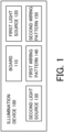
- Fig. 1 shows an illumination device 100 according to an embodiment of the present invention.
- the illumination device 100 includes a board 110, a first light source 120, a second light source 130, first wiring patterns 140, and second wiring patterns 150.
- the illumination device 100 is configured for illuminating a charging inlet of a vehicle.
- the board 110 is an element having a plate shape and has a first face 111 and a second face 112 opposite to the first face 111.
- the board 110 is made of an insulator (for example a resin and/or a glass) and transparent for light.
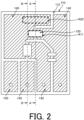
- Fig. 2 shows a view of the board 110 from its first face 111 side
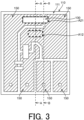
- Fig. 3 shows a view of the board 110 from its second face 112 side
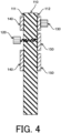
- Fig. 4 shows a sectional view of the board 110 according to Figs. 2 and 3 along the line AA
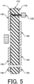
- Fig. 5 shows a sectional view of the board 110 according to Figs. 2 and 3 along the line BB.
- the first light source 120 and second light source 130 are light sources for emitting light, for example LEDs (light emitting diodes). As shown in Figs. 2 and 4 , the first light source 120 is disposed on the first face 111 of the board 110. As shown in Figs. 3 to 5 , the second light source 130 is disposed on the second face 112 of the board 110.
- the first light source 120 and the second light source 130 are intended to be used for different purposes.
- the first light source 120 is intended to be used e.g. for illumination.
- the second light source 130 is intended to be used e.g. for an indicator.
- the illumination device 100 is configured for illuminating a charging inlet of a vehicle
- the first light source 120 is configured for illuminating the charging inlet of the vehicle
- the second light source 130 is intended for an indicator
- the indicator being configured to indicate a state of charge of the vehicle (for example a state of charge of a battery (for example a main battery) of the vehicle).
- the first wiring patterns 140 are used for electrically connecting components arranged on the first face 111 of the board 110 (including the first light source 120). As shown in Figs. 2 , 4 and 5 , the first wiring patterns 140 are positioned on the first face 111 of the board 110 so that the first wiring patterns 140 are brought into contact with the first face 111.
- the second wiring patterns 150 are used for electrically connecting components arranged on the second face 112 of the board 110 (including the second light source 130). As shown in Figs. 3 to 5 , the second wiring patterns 150 are positioned on the second face 112 of the board 110 so that the second wiring patterns 150 are brought into contact with the second face 112.
- the first wiring patterns 140 and second wiring patterns 150 are made of an electrical conductor, and for example patterns of metal foils (e.g. copper foils).
- the first wiring patterns 140 and second wiring patterns 150 may be made of a same material or made of different materials.
- the second wiring pattern 150 of the illumination device 100 is disposed so as to cover a region A12 on the second face 112, the region A12 on the second face 112 opposed to a region A11 on the first face 111 with the first light source 120 disposed therein. In this manner, a light emitted from the first light source 120 toward the board 100 is blocked by the second wiring patterns 150, as shown in Fig. 4 . This means that according to the present embodiment, even when the light emitted from the first light source 120 toward the board 100 passes through the board, this light is blocked by the second wiring patterns 150.
- a light coming from the first light source 120 can be prevented from arriving at the second face 112 side of the board 100, for example by providing an element for preventing the light coming from the first light source 120 from arriving at the second face 112 side of the board 100 by circumvention (for example a cover 9 as disclosed in Patent Document 1).
- the present embodiment enables the light coming from the first light source 120 to be prevented from arriving at the second face 112 side of the board 100.
- the present embodiment enables the second light source 130 side (the second face 112 side of the board 100) to be prevented from being illuminated. Accordingly, only when the second light source 130 is turned on, the present embodiment may allow a user to recognize the fact that the second light source 130 is turned on, wherein when the second light source 130 is not turned on, the user may not recognize that the second light source 130 is turned on.
- the present embodiment allows the user to correctly recognize indication of the indicator (indication by the second light source 130) even in the case of the light source for illumination (first light source 120) being turned on.
- the present embodiment enables an illumination device to be provided which includes two light sources to be used for different purposes.
- the first wiring patterns 140 in the illumination device 100 is disposed so as to cover a region A22 on the first face 111, the region A22 on the first face 111 opposed to a region A21 on the second face 112 with the second light source 130 disposed therein. In this manner, a light emitted from the second light source 130 toward the board 100 is blocked by the first wiring patterns 140, as shown in Fig. 5 . This means that according to the present embodiment, even when the light emitted from the second light source 130 toward the board 100 passes through the board, this light is blocked by the first wiring patterns 140.
- a light coming from the second light source 130 can be prevented from arriving at the first face 111 side of the board 100, for example by providing an element for preventing the light coming from the second light source 130 from arriving at the first face 111 side of the board 100 by circumvention (for example the cover 9 as disclosed in Patent Document 1).
- the present embodiment enables the light coming from the second light source 130 to be prevented from arriving at the first face 111 side of the board 100.
- the present embodiment enables the first light source 120 side (the first face 111 side of the board 100) to be prevented from being illuminated. Accordingly, only when the first light source 120 is turned on, the present embodiment may allow the user to recognize the fact that the first light source 120 is turned on, wherein when the first light source 120 is not turned on, the user may not recognize that the first light source 120 is turned on.
- the first light source 120 may be a light source for an indicator, the indicator being configured to indicate first information
- the second light source 130 may be a light source for an indicator, the indicator being configured to indicate second information that is different from the first information.
- the present embodiment enables indications of both indicators for indicating the first information (indication via the first light source 120) and for indicating the second information (indication via the second light source 130) to be correctly recognized by the user.
Landscapes
- Engineering & Computer Science (AREA)
- General Engineering & Computer Science (AREA)
- Microelectronics & Electronic Packaging (AREA)
- Physics & Mathematics (AREA)
- Mechanical Engineering (AREA)
- Optics & Photonics (AREA)
- Theoretical Computer Science (AREA)
- General Physics & Mathematics (AREA)
- Details Of Measuring Devices (AREA)
- Fastening Of Light Sources Or Lamp Holders (AREA)
- Arrangement Of Elements, Cooling, Sealing, Or The Like Of Lighting Devices (AREA)
- Lighting Device Outwards From Vehicle And Optical Signal (AREA)
- Illuminated Signs And Luminous Advertising (AREA)
Abstract
Description
- The present invention relates to an illumination device.
- Patent Document 1 discloses an illumination device which includes two light emitters used for different purposes, i.e., a first light emitter 13A and a second light emitter 13B, wherein the first light emitter 13A is used as illumination for a charging inlet and the second light emitter 13B is used as an indicator. The illumination device as disclosed in Patent Document 1 is configured such that the first light emitter 13A and the second light emitter 13B are provided on a front side and on a back side of a board 7, respectively.
- Patent Document 1:
JP 2023-42051 A - Generally, a board is made of an insulator such as a resin and/or glass and transparent for light. In the case where light sources are arranged on two opposite faces of the board, as is in the illumination device according to Patent Document 1, a light coming from a light source on the front side may e.g. pass through the board to reach the back side of the board. As a result, a user may misrecognize that a light source on the back side of the board were turned on, despite the light source on the back side not being turned on. For example, in the case where the light source on the back side of the board is used as the indicator, as is in the illumination device according to Patent Document 1, the above-described situation may cause a user to misrecognize that the indicator were turned on, despite the light source on the back side emitting no light.
- Therefore, an object of the present invention is to provide an illumination device which includes two light sources to be used for different purposes.
- In order to achieve the above-mentioned objective, an embodiment of the present invention relates to an illumination device including: a board having a first face and a second face opposite to the first face; a first light source disposed on the first face; a second light source disposed on the second face; and a second wiring pattern disposed on the second face, wherein the second wiring pattern is disposed so as to cover a region on the second face, the region on the second face opposed to a region on the first face with the first light source disposed therein.
- The present invention enables an illumination device to be provided which includes two light sources to be used for different purposes.
-
-
Fig. 1 shows anillumination device 100 according to an embodiment of the present invention; -
Fig. 2 shows a view of aboard 110 from itsfirst face 111 side; -
Fig. 3 shows a view of theboard 110 from itssecond face 112 side; -
Fig. 4 shows a sectional view of theboard 110 according toFigs. 2 and3 along the line AA; and -
Fig. 5 shows a sectional view of theboard 110 according toFigs. 2 and3 along the line BB. -
Fig. 1 shows anillumination device 100 according to an embodiment of the present invention. Theillumination device 100 includes aboard 110, afirst light source 120, asecond light source 130,first wiring patterns 140, andsecond wiring patterns 150. For example, theillumination device 100 is configured for illuminating a charging inlet of a vehicle. - The
board 110 is an element having a plate shape and has afirst face 111 and asecond face 112 opposite to thefirst face 111. Theboard 110 is made of an insulator (for example a resin and/or a glass) and transparent for light.Fig. 2 shows a view of theboard 110 from itsfirst face 111 side,Fig. 3 shows a view of theboard 110 from itssecond face 112 side,Fig. 4 shows a sectional view of theboard 110 according toFigs. 2 and3 along the line AA, andFig. 5 shows a sectional view of theboard 110 according toFigs. 2 and3 along the line BB. - The
first light source 120 andsecond light source 130 are light sources for emitting light, for example LEDs (light emitting diodes). As shown inFigs. 2 and4 , thefirst light source 120 is disposed on thefirst face 111 of theboard 110. As shown inFigs. 3 to 5 , thesecond light source 130 is disposed on thesecond face 112 of theboard 110. - For example, the
first light source 120 and thesecond light source 130 are intended to be used for different purposes. Thefirst light source 120 is intended to be used e.g. for illumination. Thesecond light source 130 is intended to be used e.g. for an indicator. For example, when theillumination device 100 is configured for illuminating a charging inlet of a vehicle, thefirst light source 120 is configured for illuminating the charging inlet of the vehicle, wherein thesecond light source 130 is intended for an indicator, the indicator being configured to indicate a state of charge of the vehicle (for example a state of charge of a battery (for example a main battery) of the vehicle). - The
first wiring patterns 140 are used for electrically connecting components arranged on thefirst face 111 of the board 110 (including the first light source 120). As shown inFigs. 2 ,4 and5 , thefirst wiring patterns 140 are positioned on thefirst face 111 of theboard 110 so that thefirst wiring patterns 140 are brought into contact with thefirst face 111. - The
second wiring patterns 150 are used for electrically connecting components arranged on thesecond face 112 of the board 110 (including the second light source 130). As shown inFigs. 3 to 5 , thesecond wiring patterns 150 are positioned on thesecond face 112 of theboard 110 so that thesecond wiring patterns 150 are brought into contact with thesecond face 112. - The
first wiring patterns 140 andsecond wiring patterns 150 are made of an electrical conductor, and for example patterns of metal foils (e.g. copper foils). Thefirst wiring patterns 140 andsecond wiring patterns 150 may be made of a same material or made of different materials. - The
second wiring pattern 150 of theillumination device 100 according to the present embodiment is disposed so as to cover a region A12 on thesecond face 112, the region A12 on thesecond face 112 opposed to a region A11 on thefirst face 111 with thefirst light source 120 disposed therein. In this manner, a light emitted from thefirst light source 120 toward theboard 100 is blocked by thesecond wiring patterns 150, as shown inFig. 4 . This means that according to the present embodiment, even when the light emitted from thefirst light source 120 toward theboard 100 passes through the board, this light is blocked by thesecond wiring patterns 150. According to the present embodiment, a light coming from thefirst light source 120 can be prevented from arriving at thesecond face 112 side of theboard 100, for example by providing an element for preventing the light coming from thefirst light source 120 from arriving at thesecond face 112 side of theboard 100 by circumvention (for example a cover 9 as disclosed in Patent Document 1). - In the above-described manner, the present embodiment enables the light coming from the
first light source 120 to be prevented from arriving at thesecond face 112 side of theboard 100. As a result, when thesecond light source 130 emits no light, the present embodiment enables thesecond light source 130 side (thesecond face 112 side of the board 100) to be prevented from being illuminated. Accordingly, only when thesecond light source 130 is turned on, the present embodiment may allow a user to recognize the fact that thesecond light source 130 is turned on, wherein when thesecond light source 130 is not turned on, the user may not recognize that thesecond light source 130 is turned on. - Therefore, for example when the
first light source 120 is intended to be used for illumination and thesecond light source 130 is intended to be used for an indicator, the present embodiment allows the user to correctly recognize indication of the indicator (indication by the second light source 130) even in the case of the light source for illumination (first light source 120) being turned on. As a result, the present embodiment enables an illumination device to be provided which includes two light sources to be used for different purposes. - Furthermore, the
first wiring patterns 140 in theillumination device 100 according to the present embodiment is disposed so as to cover a region A22 on thefirst face 111, the region A22 on thefirst face 111 opposed to a region A21 on thesecond face 112 with thesecond light source 130 disposed therein. In this manner, a light emitted from thesecond light source 130 toward theboard 100 is blocked by thefirst wiring patterns 140, as shown inFig. 5 . This means that according to the present embodiment, even when the light emitted from thesecond light source 130 toward theboard 100 passes through the board, this light is blocked by thefirst wiring patterns 140. According to the present embodiment, a light coming from thesecond light source 130 can be prevented from arriving at thefirst face 111 side of theboard 100, for example by providing an element for preventing the light coming from thesecond light source 130 from arriving at thefirst face 111 side of theboard 100 by circumvention (for example the cover 9 as disclosed in Patent Document 1). - In the above-described manner, the present embodiment enables the light coming from the
second light source 130 to be prevented from arriving at thefirst face 111 side of theboard 100. As a result, when thefirst light source 120 emits no light, the present embodiment enables thefirst light source 120 side (thefirst face 111 side of the board 100) to be prevented from being illuminated. Accordingly, only when thefirst light source 120 is turned on, the present embodiment may allow the user to recognize the fact that thefirst light source 120 is turned on, wherein when thefirst light source 120 is not turned on, the user may not recognize that thefirst light source 120 is turned on. - The
first light source 120 may be a light source for an indicator, the indicator being configured to indicate first information, wherein thesecond light source 130 may be a light source for an indicator, the indicator being configured to indicate second information that is different from the first information. Also in such a configuration, the present embodiment enables indications of both indicators for indicating the first information (indication via the first light source 120) and for indicating the second information (indication via the second light source 130) to be correctly recognized by the user. -
- 100
- Illumination device
- 110
- Board
- 111
- First face of the
board 110 - 112
- Second face of the
board 110 - 120
- First light source
- 130
- Second light source
- 140
- First wiring patterns
- 150
- Second wiring patterns
Claims (7)
- An illumination device (100) comprising:a board (110) having a first face (111) and a second face (112) opposite to the first face (111);a first light source (120) disposed on the first face (111);a second light source (130) disposed on the second face (112); anda second wiring pattern (150) disposed on the second face (112),wherein the second wiring pattern (150) is disposed so as to cover a region (A12) on the second face (112), the region (A12) on the second face (112) opposed to a region (A11) on the first face (111) with the first light source (120) disposed therein.
- The illumination device (100) as claimed in claim 1, further comprising a first wiring pattern (140) disposed on the first face (111),
wherein the first wiring pattern (140) is disposed so as to cover a region (A22) on the first face (111), the region (A22) on the first face (111) opposed to a region (A21) on the second face (112) with the second light source (130) disposed therein. - The illumination device (100) as claimed in claim 1 or 2,
wherein the first light source (120) and the second light source (130) are intended to be used for different purposes. - The illumination device (100) as claimed in claim 3,
wherein the second light source (130) is intended to be used for an indicator. - The illumination device (100) as claimed in claim 4,
wherein the first light source (120) is intended to be used for illumination. - The illumination device (100) as claimed in claim 5,wherein the illumination device (100) is an illumination device configured for illuminating a charging inlet of a vehicle,wherein the first light source (120) is a light source configured for illuminating the charging inlet of the vehicle, andwherein the second light source (130) is a light source for an indicator, the indicator being configured to indicate a state of charge of the vehicle.
- The illumination device (100) as claimed in claim 2,wherein the first light source (120) is a light source for an indicator, the indicator being configured to indicate first information, andwherein the second light source (130) is a light source for an indicator, the indicator being configured to indicate second information that is different from the first information.
Applications Claiming Priority (1)
| Application Number | Priority Date | Filing Date | Title |
|---|---|---|---|
| JP2023100008A JP2025000251A (en) | 2023-06-19 | 2023-06-19 | Lighting device |
Publications (2)
| Publication Number | Publication Date |
|---|---|
| EP4482264A1 true EP4482264A1 (en) | 2024-12-25 |
| EP4482264B1 EP4482264B1 (en) | 2025-05-07 |
Family
ID=91465313
Family Applications (1)
| Application Number | Title | Priority Date | Filing Date |
|---|---|---|---|
| EP24180796.5A Active EP4482264B1 (en) | 2023-06-19 | 2024-06-07 | Illumination device |
Country Status (4)
| Country | Link |
|---|---|
| US (1) | US20240416832A1 (en) |
| EP (1) | EP4482264B1 (en) |
| JP (1) | JP2025000251A (en) |
| CN (1) | CN119163896A (en) |
Citations (5)
| Publication number | Priority date | Publication date | Assignee | Title |
|---|---|---|---|---|
| US20110175548A1 (en) * | 2010-01-18 | 2011-07-21 | Toshiba Lighting & Technology Corporation | Lighting apparatus |
| US8198109B2 (en) * | 2010-08-27 | 2012-06-12 | Quarkstar Llc | Manufacturing methods for solid state light sheet or strip with LEDs connected in series for general illumination |
| US20120181560A1 (en) * | 2011-01-17 | 2012-07-19 | Ibiden Co., Ltd. | Led wiring board, light emitting module, method for manufacturing led wiring board and method for manufacturing light emitting module |
| US10665576B2 (en) * | 2017-06-21 | 2020-05-26 | Stanley Electric Co., Ltd. | Optically transparent plate with light emitting function and method of producing the same |
| JP2023042051A (en) | 2021-09-14 | 2023-03-27 | 矢崎総業株式会社 | Lighting device |
Family Cites Families (3)
| Publication number | Priority date | Publication date | Assignee | Title |
|---|---|---|---|---|
| JP4873319B2 (en) * | 2007-06-04 | 2012-02-08 | 日本精機株式会社 | Display device |
| JP2017228405A (en) * | 2016-06-22 | 2017-12-28 | 東芝ライテック株式会社 | Vehicular lighting device, vehicular lighting fixture, and vehicular lighting fixture set |
| JP7113216B2 (en) * | 2017-08-25 | 2022-08-05 | パナソニックIpマネジメント株式会社 | Light emitting device and moving object |
-
2023
- 2023-06-19 JP JP2023100008A patent/JP2025000251A/en active Pending
-
2024
- 2024-06-07 EP EP24180796.5A patent/EP4482264B1/en active Active
- 2024-06-12 US US18/741,195 patent/US20240416832A1/en not_active Abandoned
- 2024-06-13 CN CN202410760910.3A patent/CN119163896A/en active Pending
Patent Citations (5)
| Publication number | Priority date | Publication date | Assignee | Title |
|---|---|---|---|---|
| US20110175548A1 (en) * | 2010-01-18 | 2011-07-21 | Toshiba Lighting & Technology Corporation | Lighting apparatus |
| US8198109B2 (en) * | 2010-08-27 | 2012-06-12 | Quarkstar Llc | Manufacturing methods for solid state light sheet or strip with LEDs connected in series for general illumination |
| US20120181560A1 (en) * | 2011-01-17 | 2012-07-19 | Ibiden Co., Ltd. | Led wiring board, light emitting module, method for manufacturing led wiring board and method for manufacturing light emitting module |
| US10665576B2 (en) * | 2017-06-21 | 2020-05-26 | Stanley Electric Co., Ltd. | Optically transparent plate with light emitting function and method of producing the same |
| JP2023042051A (en) | 2021-09-14 | 2023-03-27 | 矢崎総業株式会社 | Lighting device |
Also Published As
| Publication number | Publication date |
|---|---|
| JP2025000251A (en) | 2025-01-07 |
| CN119163896A (en) | 2024-12-20 |
| US20240416832A1 (en) | 2024-12-19 |
| EP4482264B1 (en) | 2025-05-07 |
Similar Documents
| Publication | Publication Date | Title |
|---|---|---|
| US5047761A (en) | Pointer illuminated instrument | |
| US6904866B2 (en) | Indicator | |
| CN104978910B (en) | Display device | |
| JP4208316B2 (en) | Illumination structure of meter device | |
| US4004546A (en) | Illuminated indicator gauge | |
| JP2006196395A (en) | Touch switch | |
| EP4482264A1 (en) | Illumination device | |
| US6727825B2 (en) | Structure of string resistor body in an operation panel device | |
| CN105144328A (en) | Lighting switch for display unit | |
| US8783207B2 (en) | Meter pointer device | |
| GB2066575A (en) | Illuminated keyboard | |
| US2948073A (en) | Illuminated instrument panel | |
| US20080282588A1 (en) | Display apparatus | |
| US3571585A (en) | Panel and edge lighting assembly | |
| EP3736985A1 (en) | Illuminated switch | |
| US9694744B2 (en) | Flexible lighting system and component illuminated by the system | |
| US20080316758A1 (en) | Light-emitting diode module for instrument panel | |
| WO2012153873A1 (en) | LED Lighting Unit | |
| US11383677B2 (en) | Switch device | |
| JPH0280916A (en) | Illumination device of instrument apparatus | |
| US20180130317A1 (en) | Visual signalling device for control and/or display unit | |
| JP2021017144A (en) | Illumination device for license plate | |
| US4186376A (en) | Illuminable safety and vehicle function display device | |
| EP3945755A1 (en) | Power converter | |
| KR101034594B1 (en) | Probe device for measuring instrument |
Legal Events
| Date | Code | Title | Description |
|---|---|---|---|
| PUAI | Public reference made under article 153(3) epc to a published international application that has entered the european phase |
Free format text: ORIGINAL CODE: 0009012 |
|
| STAA | Information on the status of an ep patent application or granted ep patent |
Free format text: STATUS: REQUEST FOR EXAMINATION WAS MADE |
|
| 17P | Request for examination filed |
Effective date: 20240607 |
|
| AK | Designated contracting states |
Kind code of ref document: A1 Designated state(s): AL AT BE BG CH CY CZ DE DK EE ES FI FR GB GR HR HU IE IS IT LI LT LU LV MC ME MK MT NL NO PL PT RO RS SE SI SK SM TR |
|
| GRAP | Despatch of communication of intention to grant a patent |
Free format text: ORIGINAL CODE: EPIDOSNIGR1 |
|
| STAA | Information on the status of an ep patent application or granted ep patent |
Free format text: STATUS: GRANT OF PATENT IS INTENDED |
|
| GRAS | Grant fee paid |
Free format text: ORIGINAL CODE: EPIDOSNIGR3 |
|
| GRAA | (expected) grant |
Free format text: ORIGINAL CODE: 0009210 |
|
| STAA | Information on the status of an ep patent application or granted ep patent |
Free format text: STATUS: THE PATENT HAS BEEN GRANTED |
|
| INTG | Intention to grant announced |
Effective date: 20250305 |
|
| AK | Designated contracting states |
Kind code of ref document: B1 Designated state(s): AL AT BE BG CH CY CZ DE DK EE ES FI FR GB GR HR HU IE IS IT LI LT LU LV MC ME MK MT NL NO PL PT RO RS SE SI SK SM TR |
|
| REG | Reference to a national code |
Ref country code: GB Ref legal event code: FG4D |
|
| REG | Reference to a national code |
Ref country code: CH Ref legal event code: EP |
|
| REG | Reference to a national code |
Ref country code: DE Ref legal event code: R096 Ref document number: 602024000112 Country of ref document: DE |
|
| REG | Reference to a national code |
Ref country code: IE Ref legal event code: FG4D |
|
| REG | Reference to a national code |
Ref country code: NL Ref legal event code: MP Effective date: 20250507 |
|
| PG25 | Lapsed in a contracting state [announced via postgrant information from national office to epo] |
Ref country code: FI Free format text: LAPSE BECAUSE OF FAILURE TO SUBMIT A TRANSLATION OF THE DESCRIPTION OR TO PAY THE FEE WITHIN THE PRESCRIBED TIME-LIMIT Effective date: 20250507 Ref country code: ES Free format text: LAPSE BECAUSE OF FAILURE TO SUBMIT A TRANSLATION OF THE DESCRIPTION OR TO PAY THE FEE WITHIN THE PRESCRIBED TIME-LIMIT Effective date: 20250507 Ref country code: PT Free format text: LAPSE BECAUSE OF FAILURE TO SUBMIT A TRANSLATION OF THE DESCRIPTION OR TO PAY THE FEE WITHIN THE PRESCRIBED TIME-LIMIT Effective date: 20250908 |
|
| REG | Reference to a national code |
Ref country code: LT Ref legal event code: MG9D |
|
| PG25 | Lapsed in a contracting state [announced via postgrant information from national office to epo] |
Ref country code: NO Free format text: LAPSE BECAUSE OF FAILURE TO SUBMIT A TRANSLATION OF THE DESCRIPTION OR TO PAY THE FEE WITHIN THE PRESCRIBED TIME-LIMIT Effective date: 20250807 Ref country code: GR Free format text: LAPSE BECAUSE OF FAILURE TO SUBMIT A TRANSLATION OF THE DESCRIPTION OR TO PAY THE FEE WITHIN THE PRESCRIBED TIME-LIMIT Effective date: 20250808 |
|
| PG25 | Lapsed in a contracting state [announced via postgrant information from national office to epo] |
Ref country code: PL Free format text: LAPSE BECAUSE OF FAILURE TO SUBMIT A TRANSLATION OF THE DESCRIPTION OR TO PAY THE FEE WITHIN THE PRESCRIBED TIME-LIMIT Effective date: 20250507 Ref country code: NL Free format text: LAPSE BECAUSE OF FAILURE TO SUBMIT A TRANSLATION OF THE DESCRIPTION OR TO PAY THE FEE WITHIN THE PRESCRIBED TIME-LIMIT Effective date: 20250507 |
|
| REG | Reference to a national code |
Ref country code: AT Ref legal event code: MK05 Ref document number: 1793929 Country of ref document: AT Kind code of ref document: T Effective date: 20250507 |
|
| PG25 | Lapsed in a contracting state [announced via postgrant information from national office to epo] |
Ref country code: BG Free format text: LAPSE BECAUSE OF FAILURE TO SUBMIT A TRANSLATION OF THE DESCRIPTION OR TO PAY THE FEE WITHIN THE PRESCRIBED TIME-LIMIT Effective date: 20250507 |
|
| PG25 | Lapsed in a contracting state [announced via postgrant information from national office to epo] |
Ref country code: HR Free format text: LAPSE BECAUSE OF FAILURE TO SUBMIT A TRANSLATION OF THE DESCRIPTION OR TO PAY THE FEE WITHIN THE PRESCRIBED TIME-LIMIT Effective date: 20250507 |
|
| PG25 | Lapsed in a contracting state [announced via postgrant information from national office to epo] |
Ref country code: AT Free format text: LAPSE BECAUSE OF FAILURE TO SUBMIT A TRANSLATION OF THE DESCRIPTION OR TO PAY THE FEE WITHIN THE PRESCRIBED TIME-LIMIT Effective date: 20250507 |
|
| PG25 | Lapsed in a contracting state [announced via postgrant information from national office to epo] |
Ref country code: RS Free format text: LAPSE BECAUSE OF FAILURE TO SUBMIT A TRANSLATION OF THE DESCRIPTION OR TO PAY THE FEE WITHIN THE PRESCRIBED TIME-LIMIT Effective date: 20250807 |
|
| PG25 | Lapsed in a contracting state [announced via postgrant information from national office to epo] |
Ref country code: IS Free format text: LAPSE BECAUSE OF FAILURE TO SUBMIT A TRANSLATION OF THE DESCRIPTION OR TO PAY THE FEE WITHIN THE PRESCRIBED TIME-LIMIT Effective date: 20250907 |
|
| PG25 | Lapsed in a contracting state [announced via postgrant information from national office to epo] |
Ref country code: LV Free format text: LAPSE BECAUSE OF FAILURE TO SUBMIT A TRANSLATION OF THE DESCRIPTION OR TO PAY THE FEE WITHIN THE PRESCRIBED TIME-LIMIT Effective date: 20250507 |
|
| PG25 | Lapsed in a contracting state [announced via postgrant information from national office to epo] |
Ref country code: DK Free format text: LAPSE BECAUSE OF FAILURE TO SUBMIT A TRANSLATION OF THE DESCRIPTION OR TO PAY THE FEE WITHIN THE PRESCRIBED TIME-LIMIT Effective date: 20250507 Ref country code: SM Free format text: LAPSE BECAUSE OF FAILURE TO SUBMIT A TRANSLATION OF THE DESCRIPTION OR TO PAY THE FEE WITHIN THE PRESCRIBED TIME-LIMIT Effective date: 20250507 |
|
| PG25 | Lapsed in a contracting state [announced via postgrant information from national office to epo] |
Ref country code: CZ Free format text: LAPSE BECAUSE OF FAILURE TO SUBMIT A TRANSLATION OF THE DESCRIPTION OR TO PAY THE FEE WITHIN THE PRESCRIBED TIME-LIMIT Effective date: 20250507 |
|
| PG25 | Lapsed in a contracting state [announced via postgrant information from national office to epo] |
Ref country code: EE Free format text: LAPSE BECAUSE OF FAILURE TO SUBMIT A TRANSLATION OF THE DESCRIPTION OR TO PAY THE FEE WITHIN THE PRESCRIBED TIME-LIMIT Effective date: 20250507 |
|
| PG25 | Lapsed in a contracting state [announced via postgrant information from national office to epo] |
Ref country code: SK Free format text: LAPSE BECAUSE OF FAILURE TO SUBMIT A TRANSLATION OF THE DESCRIPTION OR TO PAY THE FEE WITHIN THE PRESCRIBED TIME-LIMIT Effective date: 20250507 |
|
| PG25 | Lapsed in a contracting state [announced via postgrant information from national office to epo] |
Ref country code: IT Free format text: LAPSE BECAUSE OF FAILURE TO SUBMIT A TRANSLATION OF THE DESCRIPTION OR TO PAY THE FEE WITHIN THE PRESCRIBED TIME-LIMIT Effective date: 20250507 |
|
| REG | Reference to a national code |
Ref country code: DE Ref legal event code: R097 Ref document number: 602024000112 Country of ref document: DE |
|
| PG25 | Lapsed in a contracting state [announced via postgrant information from national office to epo] |
Ref country code: MC Free format text: LAPSE BECAUSE OF FAILURE TO SUBMIT A TRANSLATION OF THE DESCRIPTION OR TO PAY THE FEE WITHIN THE PRESCRIBED TIME-LIMIT Effective date: 20250507 |
|
| PLBE | No opposition filed within time limit |
Free format text: ORIGINAL CODE: 0009261 |
|
| STAA | Information on the status of an ep patent application or granted ep patent |
Free format text: STATUS: NO OPPOSITION FILED WITHIN TIME LIMIT |
|
| REG | Reference to a national code |
Ref country code: CH Ref legal event code: L10 Free format text: ST27 STATUS EVENT CODE: U-0-0-L10-L00 (AS PROVIDED BY THE NATIONAL OFFICE) Effective date: 20260318 |
|
| 26N | No opposition filed |
Effective date: 20260210 |
|
| PG25 | Lapsed in a contracting state [announced via postgrant information from national office to epo] |
Ref country code: FR Free format text: LAPSE BECAUSE OF NON-PAYMENT OF DUE FEES Effective date: 20250707 |