EP4482036A1 - Device and method for continuous-time energy calculation of an analog signal - Google Patents
Device and method for continuous-time energy calculation of an analog signal Download PDFInfo
- Publication number
- EP4482036A1 EP4482036A1 EP23305983.1A EP23305983A EP4482036A1 EP 4482036 A1 EP4482036 A1 EP 4482036A1 EP 23305983 A EP23305983 A EP 23305983A EP 4482036 A1 EP4482036 A1 EP 4482036A1
- Authority
- EP
- European Patent Office
- Prior art keywords
- signal
- request signal
- delayed
- req
- dir
- Prior art date
- Legal status (The legal status is an assumption and is not a legal conclusion. Google has not performed a legal analysis and makes no representation as to the accuracy of the status listed.)
- Granted
Links
Images




Classifications
-
- H—ELECTRICITY
- H03—ELECTRONIC CIRCUITRY
- H03M—CODING; DECODING; CODE CONVERSION IN GENERAL
- H03M1/00—Analogue/digital conversion; Digital/analogue conversion
- H03M1/12—Analogue/digital converters
- H03M1/124—Sampling or signal conditioning arrangements specially adapted for A/D converters
- H03M1/1245—Details of sampling arrangements or methods
- H03M1/1265—Non-uniform sampling
-
- H—ELECTRICITY
- H03—ELECTRONIC CIRCUITRY
- H03M—CODING; DECODING; CODE CONVERSION IN GENERAL
- H03M1/00—Analogue/digital conversion; Digital/analogue conversion
- H03M1/12—Analogue/digital converters
- H03M1/124—Sampling or signal conditioning arrangements specially adapted for A/D converters
- H03M1/1245—Details of sampling arrangements or methods
- H03M1/125—Asynchronous, i.e. free-running operation within each conversion cycle
-
- G—PHYSICS
- G01—MEASURING; TESTING
- G01R—MEASURING ELECTRIC VARIABLES; MEASURING MAGNETIC VARIABLES
- G01R19/00—Arrangements for measuring currents or voltages or for indicating presence or sign thereof
- G01R19/25—Arrangements for measuring currents or voltages or for indicating presence or sign thereof using digital measurement techniques
- G01R19/2506—Arrangements for conditioning or analysing measured signals, e.g. for indicating peak values ; Details concerning sampling, digitizing or waveform capturing
- G01R19/2509—Details concerning sampling, digitizing or waveform capturing
-
- H—ELECTRICITY
- H03—ELECTRONIC CIRCUITRY
- H03H—IMPEDANCE NETWORKS, e.g. RESONANT CIRCUITS; RESONATORS
- H03H17/00—Networks using digital techniques
- H03H17/02—Frequency selective networks
- H03H17/06—Non-recursive filters
-
- H—ELECTRICITY
- H03—ELECTRONIC CIRCUITRY
- H03M—CODING; DECODING; CODE CONVERSION IN GENERAL
- H03M1/00—Analogue/digital conversion; Digital/analogue conversion
- H03M1/06—Continuously compensating for, or preventing, undesired influence of physical parameters
- H03M1/0617—Continuously compensating for, or preventing, undesired influence of physical parameters characterised by the use of methods or means not specific to a particular type of detrimental influence
- H03M1/0626—Continuously compensating for, or preventing, undesired influence of physical parameters characterised by the use of methods or means not specific to a particular type of detrimental influence by filtering
-
- H—ELECTRICITY
- H03—ELECTRONIC CIRCUITRY
- H03M—CODING; DECODING; CODE CONVERSION IN GENERAL
- H03M1/00—Analogue/digital conversion; Digital/analogue conversion
- H03M1/12—Analogue/digital converters
- H03M1/1205—Multiplexed conversion systems
- H03M1/121—Interleaved, i.e. using multiple converters or converter parts for one channel
-
- G—PHYSICS
- G01—MEASURING; TESTING
- G01R—MEASURING ELECTRIC VARIABLES; MEASURING MAGNETIC VARIABLES
- G01R21/00—Arrangements for measuring electric power or power factor
- G01R21/133—Arrangements for measuring electric power or power factor by using digital technique
-
- H—ELECTRICITY
- H03—ELECTRONIC CIRCUITRY
- H03H—IMPEDANCE NETWORKS, e.g. RESONANT CIRCUITS; RESONATORS
- H03H17/00—Networks using digital techniques
- H03H2017/0072—Theoretical filter design
- H03H2017/0081—Theoretical filter design of FIR filters
Definitions
- the present invention concerns a device for continuous-time energy calculation of an analog signal.
- the invention also concerns an associated method for continuous-time energy calculation of an analog signal.
- a clock is used to sample the analog signal, and to synchronize subsequent processing operations.
- the power consumed for the discrete-time digital signal processing is constant in time, and depends on the frequency of the clock: the higher the frequency, the greater the power consumed.
- Voice signal processing is particularly relevant in keyword spotting applications, where the recognition of one keyword will result in an action being performed by a system, with applications in connected objects and real-time sensing.
- the present invention aims to solve this problem, by calculating the energy of the analog signal while reducing the power consumption.
- the invention consists in a device, for continuous-time energy calculation of an analog signal, comprising:
- the device further comprises:
- the combined request signal acts as a non-uniformly distributed time base, which is then used to track the variations in the filtered output. More specifically, it can be used as a time base to calculate the energy value associated with the filtered output.
- the energy present in the analog signal is calculated using continuous-time processing, which enables the decrease of the power consumption.
- the device comprises one or several of the following characteristics, separately, or according to any technically possible combinations:
- the invention also relates to a method for continuous-time energy calculation of an analog signal, the method being implemented by a device according of any of the preceding claims, the method comprising:
- Figure 1 is a view of an integrated device 1 according to an embodiment of the invention.
- the device 1 comprises a continuous-time analog-to-digital converter 10, or CT-ADC 10, not visible on figure 1 but visible on figure 2 , and an integrated circuit 5.
- CT-ADC continuous-time analog-to-digital converter
- the continuous-time analog-to-digital converter 10 converts an analog signal S in into a request signal REQ and a direction signal DIR, visible on figure 2 .
- the CT-ADC 10 receives the analog signal S in , which is preferentially an analog signal with a frequency equal to or below 1MHz, and outputs the request signal REQ and the direction signal DIR.
- the analog signal S in is for example an audio signal, in particular a voice signal, and the device 1 is used for voice signal processing.
- the CT-ADC 10 is characterized by a given resolution, which determines a number of a plurality of predetermined levels of the CT-ADC 10.
- the CT-ADC 10 samples the analog signal S in only if the analog signal S in crosses one of the plurality of predetermined levels.
- the predetermined levels are predetermined quantization amplitude levels of the analog signal S in and depend on the resolution of the CT-ADC 10.
- the samples generated by the CT-ADC 10 form a request signal REQ and a direction signal DIR, associated to the request signal REQ.
- the request signal REQ comprises at least one pulse and the direction signal DIR comprises at least one state.
- the request signal REQ comprises a plurality of pulses and the direction signal DIR comprises a plurality of states, each state being associated to a corresponding pulse.
- Each pulse of the request signal REQ corresponds to the analog signal S in crossing one of the predetermined level and comprises a rising edge.
- Each state on the direction signal DIR is either high state, corresponding to an increase in the amplitude level of the analog signal S in , or low, corresponding to a decrease in the amplitude level of the analog signal S in .
- the CT-ADC 10 encodes asynchronously the analog signal S in , the predetermined levels being the corresponding quantization levels.
- the CT-ADC 10 samples the analog signal S in only based on the amplitude of the analog signal S in and not based on a sampling frequency, the time between two successive rising edges in the request signal REQ is unknown and may vary.
- the integrated circuit 5 is connected to the CT-ADC 10 and comprises at least one digital processing module 14, visible on figure 2 .
- Each digital processing module 14 comprises a filtering unit 11, a pulse combiner 16 and an energy estimator 17.
- the filtering unit 11 is configured to perform continuous-time finite impulse response filtering operations.
- the filtering unit 11 comprises a delaying module 12 and a calculating module 15.
- the device 1 comprises eight digital processing modules 14 for voice processing applications, but could comprise more or less, for example between one to sixteen digital processing modules 14, and up to thirty-two or sixty-four digital processing modules 14.
- the digital processing modules 14 may share components between themselves, such as the delaying module 12, as visible on figure 1 , where one delaying module 12 is shared by all digital processing modules 14.
- all digital processing modules 14 may be fully separated and do not share any components.
- the integrated circuit 5 comprises at least one fully depleted silicon on insulator transistor, in particular at least one 28nm fully depleted silicon on insulator transistor, which is used to implement on-chip the digital processing modules 14.
- the delaying module 12 is connected to the CT-ADC 10. When the device 1 is in operation, the delaying module 12 is configured to receive the request and direction signals REQ and DIR output by the CT-ADC 10.
- the delaying module 12 comprises at least one delay block 21, and advantageously comprises a plurality of successive delay blocks 21, as shown in figure 3 .
- FIG. 3 shows three delay blocks 21 as an example, but the delaying module 12 alternatively comprises more or less delay blocks 21, for example between one and twenty delay blocks 21, for example sixteen delay blocks 21.
- Each delay block 21 delays signals it receives by a given delay time. This given delay time is advantageously configurable by external means.
- each delay block 21 is identical, and delays the signals it receives by the same delay time.
- the delay time is for example set between 10 and 100ns, for example is equal to 62.5 ⁇ s when performing voice signal processing.
- the delay blocks 21 are arranged sequentially, so that when the device 1 is in operation, an output signal of a first delay block 21 is received by a second delay block 21. Therefore, a signal passing through the delay blocks 21 is delayed by an integer multiple of the delay time, the integer multiple being equal to the number of delay blocks 21 the signal went through.
- the request signal REQ and the direction signal DIR are received by the delay blocks 21.
- a first delay block 21 thus outputs a delayed request signal and a delayed direction signal, both delayed request and direction signals being delayed by the delay time.
- the delayed direction signal maintains its association with the delayed request signal.
- the delayed request and direction signals are then received by a following delay block 21, which outputs further delayed request and direction signals.
- the delaying module 12 outputs the request signal REQ and the direction signal DIR and the delayed request and direction signals delayed by the three delay blocks 21.
- the delay blocks may not have the same behaviour and delay the signal by a different delay time.
- a signal passing through the delay blocks is delayed by the sum of all the delay times of the delay blocks it passes through.
- the calculating module 15 is connected to the delaying module 12.
- the calculating module 15 comprises at least one multiply-accumulate block 23 and a summation unit 24.
- the calculating module 15 comprises one more multiply-accumulate blocks 23 than there are delay blocks 21 in the delaying module 12.
- the calculating module 15 comprises four multiply-accumulate blocks 23, and the delaying module 12 comprises three delay blocks 21.
- a first multiply-accumulate block 23 is connected to the delaying module 12 and receives the request and direction signals REQ and DIR , and the other multiply-accumulate blocks 23 are each connected to one of the delay blocks 21 of the delaying module 12 and receive the delayed direction and request signals from each delay block 21.
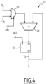
- FIG. 4 A detailed schematic of a structure of the first multiply-accumulate block 23 is shown on figure 4 .
- each multiply-accumulate block 23 has an identical structure.
- Each multiply-accumulate block 23 comprises a logic multiplexer 25, a summation unit 26 and a D flip-flop 27.
- the summation unit 26 is connected on one input to an output of the logic multiplexer 25 and on another input to an output port of the D flip-flop 27.
- the summation unit 26 is connected on an output to a data input port of the D flip-flop 27.
- Each multiply-accumulate block 23 is associated with a coefficient h i , with i an integer ranging from 0 to k-1, k being the number of multiply-accumulate blocks 23.
- k is also called a length of the filtering unit 11, and k-1 the order of the filter 11.
- k is equal to four, but may be more or less, generally between one and thirty-two.
- the coefficients h i are advantageously stored in a memory, not represented, and are received respectively by the logic multiplexers 25 of each multiply-accumulate block 23.
- the coefficients h i are advantageously configured, for example by a user of the device 1, according to the analog signal S in , and desired characteristics of the filtering unit 11.
- the coefficients h i are chosen so that one of the filtering units 11 is a band pass filter with a bandwidth comprised between 573.8Hz and 1079.5Hz with an out-of-band attenuation of 5dB.
- the following description refers to the first multiply-accumulate block 23, connected to the CT-ADC 10 and configured to receive the request and direction signals REQ and DIR. It is applicable to all the other multiply-accumulate blocks 23 by changing the request and direction signals REQ and DIR into the delayed request and direction signals.
- the logic multiplexer 25 of the first multiply-accumulate block 23 receives the value of the coefficient h 0 it is associated with, and the direction signal DIR. The logic multiplexer 25 then outputs either the value of the coefficient h 0 , or its opposite -h 0 , based on a value of the direction signal DIR. For example, if the direction signal DIR is in high state, the logic multiplexer 25 outputs the value h 0 . If the direction signal DIR is in low state, the logic multiplexer 25 outputs the value -h 0 .
- the logic multiplexer 25 outputs the value h 0 if the direction signal DIR is in low state and the logic multiplexer 25 outputs the value -h 0 if the direction signal DIR is in high state.
- This value is then added by the summation unit 26 with an output value of the D flip-flop 27 to obtain a summation value, which is received by the D flip-flop 27.
- the D flip-flop 27 also receives the request signal REQ, and when a rising edge in the request signal REQ occurs, the D flip-flop 27 is triggered and outputs an output value Y 0 of the first multiply-accumulate block 23, which is equal to the summation value.
- t n-1 , t n are successive times corresponding to a rising edge in the request signal REQ. As the rising edges are not uniform, the successive times t n-1 , and t n are not separated by a regular interval.
- the output value Y 0 is equal to zero.
- the output value Y 0 is the quantization value associated to the request signal REQ, multiplied by coefficient h 0 .
- a filtered output signal F out from the calculating module 15 is then obtained by summing the output values of all the multiply-accumulate blocks 23, which is performed by the summation unit 24.
- the filtered output signal F out is therefore a result of the finite impulse response filtering operation performed by the filter 11 on the request signal REQ and the direction signal DIR.
- the filtered output signal F out varies when the output value of each multiply-accumulate block 23 varies.
- the pulse combiner 16 is connected to the CT-ADC 10 and to all the REQ outputs of all the delay blocks 21, as presented in figure 3 .
- the pulse combiner 16 receives the request signal REQ and the delayed request signals that are output by the delay blocks 21.
- the pulse combiner 16 then outputs a combined request signal CREQ.
- the combined request signal CREQ is advantageously a concatenation of the request signal REQ and the delayed request signals received by the pulse combiner 16.
- the concatenation is advantageously performed by a logical "OR" operation.
- the pulse combiner 16 further comprises a synchronizing block, not represented, to take into account propagation delays caused by the multiply-accumulate blocks 23 and the summation unit 24, for example by adding a programmable delay, so that the combined request signal CREQ and the filtered output signal F out are synchronized.
- the combined request signal CREQ advantageously forms a non-uniformly distributed time base suitable to track variations of the filtered output signal F out .
- the energy estimator 17 is connected to the filtering unit 11 and to the pulse combiner 16.
- the energy estimator 17 advantageously comprises a D flip-flop 31, a combinatory squarer 32 and an accumulator 33, visible on figure 3 .
- the D flip-flop 31 is connected to the combinatory squarer 32.
- the D flip-flop 31 receives the filtered output signal F out and the combined pulse signal CREQ. For each rising edge of the combined pulse signal CREQ, the D flip-flop 31 is triggered and outputs a corresponding filtered output signal value, which is then received by the combinatory squarer 32.
- the combinatory squarer 32 calculates and outputs a squared filtered output signal SF out , which is the square value of the filtered output signal F out .
- the squared filtered output signal SF out is an approximation of the square value of the filtered output signal F out .
- the accumulator 33 is connected to the combinatory squarer 32.
- the accumulator 33 comprises a summation unit 35 and a resettable D flip-flop 36.
- the summation unit 35 is connected in input to the combinatory squarer 32 and to the Q output port of the resettable D flip-flop 36.
- the resettable D flip-flop 36 is further connected to an output port of the summation unit 35 and to the pulse combiner 16.
- a D flip-flop 37 is connected to the resettable D flip-flop 36.
- the squared filtered output signal SF out is received by the summation unit 35.
- the summation unit 35 adds the squared filtered output signal SF out to a stored energy value A out in the resettable D flip-flop 36 to obtain an updated energy value.
- the stored energy value A out is then modified to the updated energy value at each rising edge in the combined request signal CREQ. More precisely, the resettable flip-flop 36 outputs the updated energy value at each rising edge in the combined request signal CREQ, so that the stored energy value A out is modified to the updated energy value.
- the combined request signal CREQ acts as a time-base for energy calculation, as it is used to determine when to modify the stored energy value A out .
- the resettable D flip-flop 36 When the device 1 is in operation, the resettable D flip-flop 36 further receives a frame signal FR.
- the frame signal FR comprises at least one alternating low and high state.
- the frame signal FR comprises multiple low states alternating with multiple high states.
- the low and high states are advantageously regular, such that the frame signal FR is periodic. In variant, the frame signal FR is not periodic.
- the resettable D flip-flop 36 When the frame signal FR goes from a high state to a low state, also called a falling edge, the resettable D flip-flop 36 is reset and the D flip-flop 37 is activated.
- the D flip-flop 37 outputs an energy value E out equal to the stored energy value A out , and the stored energy value A out is set to zero.
- the stored energy value A out stays equal to zero until the frame signal FR goes from a low state to a high state, also called rising edge, at which time the stored energy value A out is modified again at each rising edge in the combined request signal CREQ, as previously described.
- the resettable D flip-flop 36 is reset and the D flip-flop 37 is activated when a rising edge occurs in the frame signal FR, and the stored energy value A out stays equal to zero until a falling edge occurs in the frame signal FR.
- the energy value E out corresponds to an approximation of an energy of the analog signal S in in a frequency range corresponding to the bandwidth of the filtering unit 11, calculated over a high state of the frame signal FR.
- the energy value E out is calculated without ponderation of the time between successive rising edges in the combined request signal CREQ.
- the energy value E out is not exactly equal to the energy of the analog signal S in .
- a discrepancy between the energy value E out and an energy value output by a similar device through discrete time digital signal processing is low, advantageously of less than 1% on average in a voice signal processing application.
- the energy value E out is advantageously used to display a spectrogram for a frequency interval corresponding to the bandwidth of the filtering unit 11, by collecting energy values E out over multiple time frames.
- the estimated energy values E out are used as features extracted from the voice signal.
- the energy values are advantageously stored in a dedicated memory unit, where additional processing, such as leading one detection and truncation of the energy values E out can be performed.
- the truncated energy values are advantageously used as input to a neural network trained to detect predetermined keywords.
- Figure 5 represents an example of an evolution of signals received and output by the accumulator 33 when the device 1 is in operation.
- the squared filtered output signal SF out is constant, equal to value A, the stored energy value A out is equal to zero, and the energy value E out is equal to zero.
- a rising edge occurs in the frame signal FR, with no impact on the values previously mentioned.
- the squared filtered output signal SF out changes, as a rising edge in the combined request signal CREQ is synchronized with a change in the filtered output signal F out .
- the stored energy A out changes as well, and becomes the updated energy value, which is a sum of the stored energy value A out and the value of the squared filtered output signal SF out before each rising edge occured.
- the squared filtered output signal SF out becomes equal to value B and the stored energy value A out becomes equal to value A.
- the squared filtered output signal SF out successively becomes equal to values C and D and A out successively becomes equal to value A+B and A+B+C.
- the energy value E out stays constant, equal to zero, or to the previous energy value E out .
- a falling edge occurs on the frame signal FR. This causes the energy value E out to become equal to the stored energy value A out , and the stored energy value A out to be reset to zero.
- a high state in the frame signal FR corresponds to a time duration over which the energy value E out is calculated.
- the value of the squared filtered signal SF out is not modified.
- the combined request signal CREQ is used as an unevenly distributed time base in order to synchronise the operation of the filtering unit 11 with the combinatory squarer 32 and the accumulator 33. More precisely, the combined request signal CREQ is used to follow every variation of the filtered output signal F out , so that the energy value E out is a function of all the variations of the filtered output signal F out .
- the operation of the device 1 requires little power due to the device 1 performing continuous-time processing. Indeed, in this case the device 1 consumes power only if the analog signal S in reaches predetermined levels. In case of silence, or low background noise, the CT-ADC 10 does not sample the analog signal S in , resulting in reduced power consumption.
- a power consumption of the microchip 5 of the device 1 is for example in a voice signal processing application, lower than 1 ⁇ W, preferentially lower than 500nW.
- a power consumption of the energy estimator 17 is lower than 5nW, preferentially lower than 2nW when detecting keywords in audio signals. The values may vary, depending on the application and the type of signal.
- the pulse combiner is not connected to all the delay blocks.
- the pulse combiner does not take into account the delayed request signals output by the delay blocks which are not connected to the pulse combiner. This results in the variations in the filtered output caused by a delay block not connected to the pulse combiner being ignored when calculating the energy values.
- some delay blocks are deactivated, and do not transmit delayed request signals to the pulse combiner. Both cases allow to obtain an effect similar to modifying the order of the filtering unit without changing an architecture of the filtering unit.
- the user determines if the pulse combiner is connected to all the delay blocks or not, and if not, to which delay blocks the pulse combiner is connected, or which delay blocks are deactivated.
- Filtering the request signal REQ and direction signal DIR is then performed. More precisely, the filtering is a finite impulse response filtering operation and results in outputting the filtered output signal F out . Filtering consists in two steps, a step S102 and a step S103.
- Step S102 consists in delaying the request signal REQ and the associated direction signal DIR.
- Step S102 results in the output of at least one delayed request signal, and the at least one delayed direction signal associated to the at least one delayed request signal.
- the delayed request signal is delayed from the request signal REQ by the delay time, and the delayed direction signal is delayed from the direction signal DIR by the same delay time.
- a plurality of delayed request signals, and a plurality of delayed direction signals associated to the delayed request signals are output, as well as the request signal DIR and direction signal REQ.
- step S102 is performed by the delaying module 12.
- Step S103 consists in calculating the filtered output signal F out from the request signal REQ, the direction signal DIR, the delayed request signals and the delayed direction signals.
- a step S104 of combining the request signal REQ and the at least one delayed request signal is then performed.
- the combination of the request signal REQ and the at least one delayed request signal results in the combined request signal CREQ.
- Step S104 is advantageously performed by the pulse combiner 16.
- a step S105 of computing the stored energy value A out associated with each rising edge of the combined request signal CREQ using the filtered output signal F out is performed.
- the squared filtered output signal SF out is first output and the value of the stored energy value A out is computed from the squared filtered output signal SF out .
- Step S105 is advantageously performed by the accumulator 33.
- a step of outputting the energy value E out is performed when a falling edge occurs on the frame signal FR.
- the device 1 performs low power energy calculation of the analog signal S in , through continuous-time digital processing.
- the pulse combiner 16 of the device 1 allows to create a time base usable to output the energy value E out , therefore making continuous-time digital processing compatible with energy calculations.
- a difference between the energy value E out output by the device 1 and an energy value output by a similar device using discrete time digital processing is low, with for example the discrepancy being of less than 1% on average in voice signal processing applications.
- using the device 1 resulted in 90.08% accuracy, and using a similar device performing discrete-time signal processing resulted in 90.21% accuracy.
- the number of digital processing modules 14, the order of the filtering unit 11 and the number of energy estimators 17 are advantageously chosen depending on an application desired by the user. For example, choosing eight digital processing modules 14, with filtering units 11 with an order of sixteen allows the user to process an audio analog signal S in corresponding to a voice signal.
Landscapes
- Engineering & Computer Science (AREA)
- Theoretical Computer Science (AREA)
- Physics & Mathematics (AREA)
- Computer Hardware Design (AREA)
- Mathematical Physics (AREA)
- General Physics & Mathematics (AREA)
- Compression, Expansion, Code Conversion, And Decoders (AREA)
Abstract
- a continuous-time analog-to-digital converter which is configured to convert the analog signal into a request signal (REQ), and a direction signal (DIR) ;
- at least one filtering unit (11), configured to output a filtered output signal (Fout), and comprising a delaying module (12) and a calculating module (15), connected to the delaying module (12) and configured calculate the filtered output signal (Fout).
According to the invention, the device (1) further comprises:
- at least one pulse combiner (16), connected to the delaying module (12) and configured to output a combined request signal (CREQ); and
- at least one energy estimator (17), connected to the filtering unit (11) and to the pulse combiner (16), configured to compute a stored energy value (Aout) associated with each pulse of the combined request signal (CREQ).
Description
- The present invention concerns a device for continuous-time energy calculation of an analog signal.
- The invention also concerns an associated method for continuous-time energy calculation of an analog signal.
- To calculate the energy from an analog signal, it is well known to perform discrete-time digital signal processing. In this case, a clock is used to sample the analog signal, and to synchronize subsequent processing operations. In this case, the power consumed for the discrete-time digital signal processing is constant in time, and depends on the frequency of the clock: the higher the frequency, the greater the power consumed.
- This leads to high power consumption, which is wasteful in particular in settings where the analog signal is sparse. This is the case for example in voice signal processing, where a voice signal can alternate with long periods of silence or of non-significant noise. Voice signal processing is particularly relevant in keyword spotting applications, where the recognition of one keyword will result in an action being performed by a system, with applications in connected objects and real-time sensing.
- To decrease power consumption, it is known to perform continuous-time digital signal processing, and in particular, continuous-time non-uniform amplitude sampling of the analog signal. However, this leads to the absence of a time reference, making it impossible to calculate an energy value from the analog signal.
- The present invention aims to solve this problem, by calculating the energy of the analog signal while reducing the power consumption.
- To this end, the invention consists in a device, for continuous-time energy calculation of an analog signal, comprising:
- a continuous-time analog-to-digital converter, configured to convert the analog signal into a request signal, the request signal comprising at least one pulse, each pulse being representative of the analog signal crossing one of a plurality of predetermined levels, and a direction signal, associated to the request signal, the direction signal being representative of a direction of the level crossing;
- at least one filtering unit, configured to perform a continuous-time finite impulse response filtering operation, the at least one filtering unit being configured to receive the request signal, the direction signal, and to output a filtered output signal, the at least one filtering unit comprising:
- o a delaying module, configured to receive the request signal and the direction signal, and to output at least one delayed request signal, delayed from the request signal by a delay time, and at least one delayed direction signal, delayed from the direction signal by the delay time, the at least one delayed request signal being associated with one of the at least one delayed direction signal; and
- o a calculating module, connected to the delaying module the calculating unit being configured to receive the request signal, the direction signal, the at least one delayed request signal and the at least one delayed direction signal and to calculate the filtered output signal.
- According to the invention, the device further comprises:
- at least one pulse combiner, connected to the delaying module, the at least one pulse combiner being configured to receive the request signal and the at least one delayed request signal and to output a combined request signal; and
- at least one energy estimator, connected to the filtering unit and to the pulse combiner, the at least one energy estimator being configured to receive the filtered output signal and the combined request signal and configured to compute a stored energy value associated with each pulse of the combined request signal..
- Advantageously, the combined request signal acts as a non-uniformly distributed time base, which is then used to track the variations in the filtered output. More specifically, it can be used as a time base to calculate the energy value associated with the filtered output. Thus, the energy present in the analog signal is calculated using continuous-time processing, which enables the decrease of the power consumption.
- According to certain embodiments of the invention, the device comprises one or several of the following characteristics, separately, or according to any technically possible combinations:
- The combined request signal is a result of a concatenation of the request signal and the at least one delayed request signal.
- The delaying module comprises a plurality of successive delay blocks, each delay block applying said delay time, a delayed request signal and a delayed direction signal being obtained as an output of each delay block.
- The at least one calculating module comprises a plurality of multiply-accumulate blocks, each multiply-accumulate block receiving one of the plurality of delayed request signals and the delayed direction signal associated to the delayed request signal, or the request signal and direction signal.
- Each multiply-accumulate block is associated with a coefficient.
- The at least one pulse combiner is configured to receive all or only some of the plurality of delayed request and associated direction signals.
- The at least one energy estimator comprises:
- a combinatory squarer configured to output a squared filtered output signal at each rising edge of the combined request signal;
- an accumulator, configured to add the squared filtered output signal to a stored energy value to obtain an updated energy value and to set a value of the stored energy value to the updated energy value at each rising edge of the combined request signal, and the accumulator is further configured to receive a frame signal, comprising alternating high states and low states, and the frame signal goes from a high state to a low state, to output the stored energy value and then set the stored energy value to zero.
- The device comprises a plurality of energy estimators, each energy estimator being configured to receive a different frame signal.
- The delaying module and/or the at least one calculating module and/or the at least one pulse combiner and/or the at least one energy estimator is implemented on an integrated circuit comprising at least one fully depleted silicon on insulator transistor.
- The invention also relates to a method for continuous-time energy calculation of an analog signal, the method being implemented by a device according of any of the preceding claims, the method comprising:
- converting the analog signal into the request signal, the request signal comprising at least one pulse, each pulse being representative of the analog signal crossing one of the plurality of predetermined levels, and into the direction signal, associated to the request signal, the direction signal being representative of the direction of the level crossing;
- filtering the request signal and the direction signal by a finite impulse response filtering operation
- the filtering comprising:
- o delaying the request signal and the associated direction signal to output the at least one delayed request signal, delayed from the request signal by the delay time, and the delayed direction signal associated to the at least one delayed request signal, delayed from the direction signal by the delay time;
- o calculating from the request signal, the direction signal, the at least one delayed request signal and the at least one delayed direction signal the filtered output signal;
- combining the request signal and the at least one delayed request signal into the combined request signal acting as a non-uniform time base; and
- The features and advantages of the invention will appear upon reading the following description, given only as an example and not limited to the following description, and making reference to the enclosed drawings, wherein:
- [
Fig. 1] figure 1 is a top view of an integrated circuit according to an embodiment of the invention; - [
Fig. 2] figure 2 is a schematic of the device offigure 1 ; - [
Fig. 3] figure 3 is a detailed schematic of the device; - [
Fig. 4] figure 4 is a schematic of detail IV offigure 3 ; - [
Fig. 5 ] is a graph showing states of the device during its operation as a function of time; and - [
Fig. 6 ] is a flowchart of a method according to an embodiment of the invention. -
Figure 1 is a view of an integrateddevice 1 according to an embodiment of the invention. Thedevice 1 comprises a continuous-time analog-to-digital converter 10, or CT-ADC 10, not visible onfigure 1 but visible onfigure 2 , and anintegrated circuit 5. - When the
device 1 is in operation, the continuous-time analog-to-digital converter 10 converts an analog signal Sin into a request signal REQ and a direction signal DIR, visible onfigure 2 . In other words, the CT-ADC 10 receives the analog signal Sin, which is preferentially an analog signal with a frequency equal to or below 1MHz, and outputs the request signal REQ and the direction signal DIR. The analog signal Sin is for example an audio signal, in particular a voice signal, and thedevice 1 is used for voice signal processing. - The CT-
ADC 10 is characterized by a given resolution, which determines a number of a plurality of predetermined levels of the CT-ADC 10. The CT-ADC 10 samples the analog signal Sin only if the analog signal Sin crosses one of the plurality of predetermined levels. The predetermined levels are predetermined quantization amplitude levels of the analog signal Sin and depend on the resolution of the CT-ADC 10.The samples generated by the CT-ADC 10 form a request signal REQ and a direction signal DIR, associated to the request signal REQ. The request signal REQ comprises at least one pulse and the direction signal DIR comprises at least one state. In general, the request signal REQ comprises a plurality of pulses and the direction signal DIR comprises a plurality of states, each state being associated to a corresponding pulse. Each pulse of the request signal REQ corresponds to the analog signal Sin crossing one of the predetermined level and comprises a rising edge. Each state on the direction signal DIR is either high state, corresponding to an increase in the amplitude level of the analog signal Sin, or low, corresponding to a decrease in the amplitude level of the analog signal Sin. In other terms, the CT-ADC 10 encodes asynchronously the analog signal Sin, the predetermined levels being the corresponding quantization levels. - As the CT-
ADC 10 samples the analog signal Sin only based on the amplitude of the analog signal Sin and not based on a sampling frequency, the time between two successive rising edges in the request signal REQ is unknown and may vary. - The
integrated circuit 5 is connected to the CT-ADC 10 and comprises at least onedigital processing module 14, visible onfigure 2 . Eachdigital processing module 14 comprises afiltering unit 11, apulse combiner 16 and anenergy estimator 17. Thefiltering unit 11 is configured to perform continuous-time finite impulse response filtering operations. Thefiltering unit 11 comprises adelaying module 12 and a calculatingmodule 15. - In
figures 2 to 4 , only onedigital processing module 14 is represented and does not share thedelaying module 12 with otherdigital processing modules 14. As an alternative, thedevice 1 comprises eightdigital processing modules 14 for voice processing applications, but could comprise more or less, for example between one to sixteendigital processing modules 14, and up to thirty-two or sixty-fourdigital processing modules 14. Thedigital processing modules 14 may share components between themselves, such as thedelaying module 12, as visible onfigure 1 , where onedelaying module 12 is shared by alldigital processing modules 14. Alternatively, alldigital processing modules 14 may be fully separated and do not share any components. Advantageously, theintegrated circuit 5 comprises at least one fully depleted silicon on insulator transistor, in particular at least one 28nm fully depleted silicon on insulator transistor, which is used to implement on-chip thedigital processing modules 14. - The
delaying module 12 is connected to the CT-ADC 10. When thedevice 1 is in operation, the delayingmodule 12 is configured to receive the request and direction signals REQ and DIR output by the CT-ADC 10. Thedelaying module 12 comprises at least onedelay block 21, and advantageously comprises a plurality of successive delay blocks 21, as shown infigure 3 . -
Figure 3 shows threedelay blocks 21 as an example, but thedelaying module 12 alternatively comprises more or less delay blocks 21, for example between one and twenty delay blocks 21, for example sixteen delay blocks 21. Eachdelay block 21 delays signals it receives by a given delay time. This given delay time is advantageously configurable by external means. In the example of the figures, eachdelay block 21 is identical, and delays the signals it receives by the same delay time. The delay time is for example set between 10 and 100ns, for example is equal to 62.5µs when performing voice signal processing. - The delay blocks 21 are arranged sequentially, so that when the
device 1 is in operation, an output signal of afirst delay block 21 is received by asecond delay block 21. Therefore, a signal passing through the delay blocks 21 is delayed by an integer multiple of the delay time, the integer multiple being equal to the number of delay blocks 21 the signal went through. - In the examples of
figures 2 to 4 , the request signal REQ and the direction signal DIR are received by the delay blocks 21. Afirst delay block 21 thus outputs a delayed request signal and a delayed direction signal, both delayed request and direction signals being delayed by the delay time. Thus, the delayed direction signal maintains its association with the delayed request signal. The delayed request and direction signals are then received by a followingdelay block 21, which outputs further delayed request and direction signals. Thedelaying module 12 outputs the request signal REQ and the direction signal DIR and the delayed request and direction signals delayed by the three delay blocks 21. - In a variant, not represented, the delay blocks may not have the same behaviour and delay the signal by a different delay time. In this case, a signal passing through the delay blocks is delayed by the sum of all the delay times of the delay blocks it passes through.
- The calculating
module 15 is connected to thedelaying module 12. The calculatingmodule 15 comprises at least one multiply-accumulateblock 23 and asummation unit 24. Advantageously, the calculatingmodule 15 comprises one more multiply-accumulateblocks 23 than there aredelay blocks 21 in thedelaying module 12. In the example shown onfigure 3 , the calculatingmodule 15 comprises four multiply-accumulateblocks 23, and thedelaying module 12 comprises three delay blocks 21. - A first multiply-accumulate
block 23 is connected to thedelaying module 12 and receives the request and direction signals REQ and DIR , and the other multiply-accumulateblocks 23 are each connected to one of the delay blocks 21 of thedelaying module 12 and receive the delayed direction and request signals from eachdelay block 21. - A detailed schematic of a structure of the first multiply-accumulate
block 23 is shown onfigure 4 . - In the example of the figures, each multiply-accumulate
block 23 has an identical structure. Each multiply-accumulateblock 23 comprises alogic multiplexer 25, asummation unit 26 and a D flip-flop 27. Thesummation unit 26 is connected on one input to an output of thelogic multiplexer 25 and on another input to an output port of the D flip-flop 27. Thesummation unit 26 is connected on an output to a data input port of the D flip-flop 27. - Each multiply-accumulate
block 23 is associated with a coefficient hi, with i an integer ranging from 0 to k-1, k being the number of multiply-accumulateblocks 23. In other terms, k is also called a length of thefiltering unit 11, and k-1 the order of thefilter 11. - In the example shown in
figure 3 , k is equal to four, but may be more or less, generally between one and thirty-two. The coefficients hi are advantageously stored in a memory, not represented, and are received respectively by thelogic multiplexers 25 of each multiply-accumulateblock 23. The coefficients hi are advantageously configured, for example by a user of thedevice 1, according to the analog signal Sin, and desired characteristics of thefiltering unit 11. - For example, in the case of voice signal processing, the coefficients hi are chosen so that one of the
filtering units 11 is a band pass filter with a bandwidth comprised between 573.8Hz and 1079.5Hz with an out-of-band attenuation of 5dB. - The following description refers to the first multiply-accumulate
block 23, connected to the CT-ADC 10 and configured to receive the request and direction signals REQ and DIR. It is applicable to all the other multiply-accumulateblocks 23 by changing the request and direction signals REQ and DIR into the delayed request and direction signals. - When the
device 1 is in operation, thelogic multiplexer 25 of the first multiply-accumulateblock 23 receives the value of the coefficient h0 it is associated with, and the direction signal DIR. Thelogic multiplexer 25 then outputs either the value of the coefficient h0, or its opposite -h0, based on a value of the direction signal DIR. For example, if the direction signal DIR is in high state, thelogic multiplexer 25 outputs the value h0. If the direction signal DIR is in low state, thelogic multiplexer 25 outputs the value -h0. As an alternative, thelogic multiplexer 25 outputs the value h0 if the direction signal DIR is in low state and thelogic multiplexer 25 outputs the value -h0 if the direction signal DIR is in high state. This value is then added by thesummation unit 26 with an output value of the D flip-flop 27 to obtain a summation value, which is received by the D flip-flop 27. The D flip-flop 27 also receives the request signal REQ, and when a rising edge in the request signal REQ occurs, the D flip-flop 27 is triggered and outputs an output value Y0 of the first multiply-accumulateblock 23, which is equal to the summation value. - In other words, the output value Y0 of the first multiply-accumulate
block 23 is determined by the following equation:
- tn-1, tn are successive times corresponding to a rising edge in the request signal REQ. As the rising edges are not uniform, the successive times tn-1, and tn are not separated by a regular interval.
- Initially, the output value Y0 is equal to zero. The output value Y0 is the quantization value associated to the request signal REQ, multiplied by coefficient h0.
- A filtered output signal Fout from the calculating
module 15 is then obtained by summing the output values of all the multiply-accumulateblocks 23, which is performed by thesummation unit 24. The filtered output signal Fout is therefore a result of the finite impulse response filtering operation performed by thefilter 11 on the request signal REQ and the direction signal DIR. The filtered output signal Fout varies when the output value of each multiply-accumulateblock 23 varies. - The
pulse combiner 16 is connected to the CT-ADC 10 and to all the REQ outputs of all the delay blocks 21, as presented infigure 3 . When thedevice 1 is in operation, thepulse combiner 16 receives the request signal REQ and the delayed request signals that are output by the delay blocks 21. Thepulse combiner 16 then outputs a combined request signal CREQ. The combined request signal CREQ is advantageously a concatenation of the request signal REQ and the delayed request signals received by thepulse combiner 16. The concatenation is advantageously performed by a logical "OR" operation. Optionally, thepulse combiner 16 further comprises a synchronizing block, not represented, to take into account propagation delays caused by the multiply-accumulateblocks 23 and thesummation unit 24, for example by adding a programmable delay, so that the combined request signal CREQ and the filtered output signal Fout are synchronized. The combined request signal CREQ advantageously forms a non-uniformly distributed time base suitable to track variations of the filtered output signal Fout. - The
energy estimator 17 is connected to thefiltering unit 11 and to thepulse combiner 16. Theenergy estimator 17 advantageously comprises a D flip-flop 31, a combinatory squarer 32 and anaccumulator 33, visible onfigure 3 . - The D flip-
flop 31 is connected to thecombinatory squarer 32. - When the
device 1 is in operation, the D flip-flop 31 receives the filtered output signal Fout and the combined pulse signal CREQ. For each rising edge of the combined pulse signal CREQ, the D flip-flop 31 is triggered and outputs a corresponding filtered output signal value, which is then received by thecombinatory squarer 32. The combinatory squarer 32 calculates and outputs a squared filtered output signal SFout, which is the square value of the filtered output signal Fout. - In a variant, the squared filtered output signal SFout is an approximation of the square value of the filtered output signal Fout.
- The
accumulator 33 is connected to thecombinatory squarer 32. Theaccumulator 33 comprises asummation unit 35 and a resettable D flip-flop 36. Thesummation unit 35 is connected in input to the combinatory squarer 32 and to the Q output port of the resettable D flip-flop 36. The resettable D flip-flop 36 is further connected to an output port of thesummation unit 35 and to thepulse combiner 16. A D flip-flop 37 is connected to the resettable D flip-flop 36. - When the
device 1 is in operation, the squared filtered output signal SFout is received by thesummation unit 35. Thesummation unit 35 adds the squared filtered output signal SFout to a stored energy value Aout in the resettable D flip-flop 36 to obtain an updated energy value. The stored energy value Aout is then modified to the updated energy value at each rising edge in the combined request signal CREQ. More precisely, the resettable flip-flop 36 outputs the updated energy value at each rising edge in the combined request signal CREQ, so that the stored energy value Aout is modified to the updated energy value. - The combined request signal CREQ acts as a time-base for energy calculation, as it is used to determine when to modify the stored energy value Aout.
- When the
device 1 is in operation, the resettable D flip-flop 36 further receives a frame signal FR. The frame signal FR comprises at least one alternating low and high state. In general, the frame signal FR comprises multiple low states alternating with multiple high states. The low and high states are advantageously regular, such that the frame signal FR is periodic. In variant, the frame signal FR is not periodic. - When the frame signal FR goes from a high state to a low state, also called a falling edge, the resettable D flip-
flop 36 is reset and the D flip-flop 37 is activated. The D flip-flop 37 outputs an energy value Eout equal to the stored energy value Aout, and the stored energy value Aout is set to zero. The stored energy value Aout stays equal to zero until the frame signal FR goes from a low state to a high state, also called rising edge, at which time the stored energy value Aout is modified again at each rising edge in the combined request signal CREQ, as previously described. - As an alternative, the resettable D flip-
flop 36 is reset and the D flip-flop 37 is activated when a rising edge occurs in the frame signal FR, and the stored energy value Aout stays equal to zero until a falling edge occurs in the frame signal FR. - The energy value Eout corresponds to an approximation of an energy of the analog signal Sin in a frequency range corresponding to the bandwidth of the
filtering unit 11, calculated over a high state of the frame signal FR. As the rising edges comprised in the combined request signal CREQ are not distributed uniformly and the time between two successive rising edges in the combined request signal CREQ may vary, the energy value Eout is calculated without ponderation of the time between successive rising edges in the combined request signal CREQ. In other words, even though the time between two rising edges in the combined request signal CREQ may vary, when calculating the energy value Eout, it is considered that all the rising edges in the combined request signal CREQ are evenly distributed. Thus, the energy value Eout is not exactly equal to the energy of the analog signal Sin. A discrepancy between the energy value Eout and an energy value output by a similar device through discrete time digital signal processing is low, advantageously of less than 1% on average in a voice signal processing application. - The energy value Eout is advantageously used to display a spectrogram for a frequency interval corresponding to the bandwidth of the
filtering unit 11, by collecting energy values Eout over multiple time frames. - Alternatively, for voice signal processing applications such as keyword spotting, the estimated energy values Eout are used as features extracted from the voice signal. The energy values are advantageously stored in a dedicated memory unit, where additional processing, such as leading one detection and truncation of the energy values Eout can be performed. The truncated energy values are advantageously used as input to a neural network trained to detect predetermined keywords.
-
Figure 5 represents an example of an evolution of signals received and output by theaccumulator 33 when thedevice 1 is in operation. - During phase P10, before a rising edge occurs in the combined request signal CREQ, the squared filtered output signal SFout is constant, equal to value A, the stored energy value Aout is equal to zero, and the energy value Eout is equal to zero. A rising edge occurs in the frame signal FR, with no impact on the values previously mentioned.
- At each phase P11, P12 and P13, which each correspond to a rising edge at the combined request signal CREQ, the squared filtered output signal SFout changes, as a rising edge in the combined request signal CREQ is synchronized with a change in the filtered output signal Fout. The stored energy Aout changes as well, and becomes the updated energy value, which is a sum of the stored energy value Aout and the value of the squared filtered output signal SFout before each rising edge occured. In the example of
figure 5 , after phase P11, the squared filtered output signal SFout becomes equal to value B and the stored energy value Aout becomes equal to value A. Similarly, after phases P12 and P13, but before phase P14, the squared filtered output signal SFout successively becomes equal to values C and D and Aout successively becomes equal to value A+B and A+B+C. The energy value Eout stays constant, equal to zero, or to the previous energy value Eout. - At phase P14, a falling edge occurs on the frame signal FR. This causes the energy value Eout to become equal to the stored energy value Aout, and the stored energy value Aout to be reset to zero. Thus, a high state in the frame signal FR corresponds to a time duration over which the energy value Eout is calculated. The value of the squared filtered signal SFout is not modified.
- The combined request signal CREQ is used as an unevenly distributed time base in order to synchronise the operation of the
filtering unit 11 with the combinatory squarer 32 and theaccumulator 33. More precisely, the combined request signal CREQ is used to follow every variation of the filtered output signal Fout, so that the energy value Eout is a function of all the variations of the filtered output signal Fout. - The operation of the
device 1 requires little power due to thedevice 1 performing continuous-time processing. Indeed, in this case thedevice 1 consumes power only if the analog signal Sin reaches predetermined levels. In case of silence, or low background noise, the CT-ADC 10 does not sample the analog signal Sin, resulting in reduced power consumption. A power consumption of themicrochip 5 of thedevice 1 is for example in a voice signal processing application, lower than 1µW, preferentially lower than 500nW. In particular, a power consumption of theenergy estimator 17 is lower than 5nW, preferentially lower than 2nW when detecting keywords in audio signals. The values may vary, depending on the application and the type of signal. - In a variant not represented, the pulse combiner is not connected to all the delay blocks. In this case, the pulse combiner does not take into account the delayed request signals output by the delay blocks which are not connected to the pulse combiner. This results in the variations in the filtered output caused by a delay block not connected to the pulse combiner being ignored when calculating the energy values. As an alternative, some delay blocks are deactivated, and do not transmit delayed request signals to the pulse combiner. Both cases allow to obtain an effect similar to modifying the order of the filtering unit without changing an architecture of the filtering unit. Advantageously, the user determines if the pulse combiner is connected to all the delay blocks or not, and if not, to which delay blocks the pulse combiner is connected, or which delay blocks are deactivated.
- In a variant not represented, each digital processing module comprises more than one energy estimator, for example three energy estimators. When the device is in operation, the energy estimators of the same digital processing module advantageously receive a different frame signal. The frame signals advantageously overlap. The energy value can thus be calculated over different overlapping time durations.
- A method for calculating the energy value Eout is now described in relation to
figure 6 . - A step S101 consists in converting the analog signal Sin. The analog signal Sin is converted into the request signal REQ and the direction signal DIR associated to the request signal REQ. The request signal REQ comprises at least one pulse comprising a rising edge, each pulse being representative of the analog signal Sin crossing one of the plurality of predetermined levels, as described previously. The direction signal DIR is representative of the direction of the level crossing. Step S101 is advantageously performed by the CT-
ADC 10. - Filtering the request signal REQ and direction signal DIR is then performed. More precisely, the filtering is a finite impulse response filtering operation and results in outputting the filtered output signal Fout. Filtering consists in two steps, a step S102 and a step S103.
- Step S102 consists in delaying the request signal REQ and the associated direction signal DIR. Step S102 results in the output of at least one delayed request signal, and the at least one delayed direction signal associated to the at least one delayed request signal. The delayed request signal is delayed from the request signal REQ by the delay time, and the delayed direction signal is delayed from the direction signal DIR by the same delay time. Advantageously, and as shown in the figures, a plurality of delayed request signals, and a plurality of delayed direction signals associated to the delayed request signals are output, as well as the request signal DIR and direction signal REQ. Advantageously, step S102 is performed by the delaying
module 12. - Step S103 consists in calculating the filtered output signal Fout from the request signal REQ, the direction signal DIR, the delayed request signals and the delayed direction signals.
- A step S104 of combining the request signal REQ and the at least one delayed request signal is then performed. The combination of the request signal REQ and the at least one delayed request signal results in the combined request signal CREQ. Step S104 is advantageously performed by the
pulse combiner 16. - A step S105 of computing the stored energy value Aout associated with each rising edge of the combined request signal CREQ using the filtered output signal Fout is performed. The squared filtered output signal SFout is first output and the value of the stored energy value Aout is computed from the squared filtered output signal SFout. Step S105 is advantageously performed by the
accumulator 33. - A step of outputting the energy value Eout is performed when a falling edge occurs on the frame signal FR.
- The
device 1 performs low power energy calculation of the analog signal Sin, through continuous-time digital processing. Thepulse combiner 16 of thedevice 1 allows to create a time base usable to output the energy value Eout, therefore making continuous-time digital processing compatible with energy calculations. - Advantageously, as previously mentioned, even though the rising edges comprised in the combined request signal CREQ are not distributed uniformly, a difference between the energy value Eout output by the
device 1 and an energy value output by a similar device using discrete time digital processing is low, with for example the discrepancy being of less than 1% on average in voice signal processing applications. This allows the enegy value Eout to be exploited in a similar way as the energy value which is obtained through discrete time digital processing. In an application using voice signal processing for keyword recognition by a convolutional neural network, using thedevice 1 resulted in 90.08% accuracy, and using a similar device performing discrete-time signal processing resulted in 90.21% accuracy. The number ofdigital processing modules 14, the order of thefiltering unit 11 and the number ofenergy estimators 17 are advantageously chosen depending on an application desired by the user. For example, choosing eightdigital processing modules 14, with filteringunits 11 with an order of sixteen allows the user to process an audio analog signal Sin corresponding to a voice signal.
Claims (10)
- Device (1), for continuous-time energy calculation of an analog signal (Sin), comprising:- a continuous-time analog-to-digital converter (10), configured to convert the analog signal (Sin) into a request signal (REQ), the request signal (REQ) comprising at least one pulse, each pulse being representative of the analog signal (Sin) crossing one of a plurality of predetermined levels, and a direction signal (DIR), associated to the request signal (REQ), the direction signal (DIR) being representative of a direction of the level crossing;- at least one filtering unit (11), configured to perform a continuous-time finite impulse response filtering operation, the at least one filtering unit (11) being configured to receive the request signal (REQ), the direction signal (DIR), and to output a filtered output signal (Fout), the at least one filtering unit (11) comprising:characterized in that the device (1) further comprises:o a delaying module (12), configured to receive the request signal (REQ) and the direction signal (DIR), and to output at least one delayed request signal, delayed from the request signal (REQ) by a delay time, and at least one delayed direction signal, delayed from the direction signal (DIR) by the delay time, the at least one delayed request signal being associated with one of the at least one delayed direction signal; ando a calculating module (15), connected to the delaying module (12) the calculating module (15) being configured to receive the request signal (REQ), the direction signal (DIR), the at least one delayed request signal and the at least one delayed direction signal and to calculate the filtered output signal (Fout);- at least one pulse combiner (16), connected to the delaying module (12), the at least one pulse combiner (16) being configured to receive the request signal (REQ) and the at least one delayed request signal and to output a combined request signal (CREQ); and- at least one energy estimator (17), connected to the filtering unit (11) and to the pulse combiner (16), the at least one energy estimator (17) being configured to receive the filtered output signal (Fout) and the combined request signal (CREQ) and configured to compute a stored energy value (Aout) associated with each pulse of the combined request signal (CREQ).
- Device (1) according to claim 1, wherein the combined request signal (CREQ) is a result of a concatenation of the request signal (REQ) and the at least one delayed request signal.
- Device (1) according to any of the preceding claims, wherein the delaying module (12) comprises a plurality of successive delay blocks (21), each delay block (21) applying said delay time, a delayed request signal and a delayed direction signal being obtained as an output of each delay block (21).
- Device (1) according to claim 3, wherein the at least one calculating module (15) comprises a plurality of multiply-accumulate blocks (23), each multiply-accumulate block (23) receiving one of the plurality of delayed request signals and the delayed direction signal associated to the delayed request signal, or the request signal (REQ) and direction signal (DIR).
- Device (1) according to claim 4, wherein each multiply-accumulate block (23) is associated with a coefficient (hi).
- Device (1) according to any of claims 4 or 5, wherein the at least one pulse combiner (16) is configured to receive all or only some of the plurality of delayed request and associated direction signals.
- Device (1) according to claim 1, wherein the at least one energy estimator (17) comprises:- a combinatory squarer (32) configured to output a squared filtered output signal (SFout) at each rising edge of the combined request signal (CREQ);- an accumulator (33), configured to add the squared filtered output signal (SFout) to a stored energy value (Aout) to obtain an updated energy value and to set a value of the stored energy value (Aout) to the updated energy value at each rising edge of the combined request signal (CREQ), and wherein the accumulator (33) is further configured to receive a frame signal (FR), comprising alternating high states and low states, and when the frame signal (FR) goes from a high state to a low state, to output the stored energy value (Aout) and then set the stored energy value (Aout) to zero.
- Device (1) according to claim 7, comprising a plurality of energy estimators (17), each energy estimator (17) being configured to receive a different frame signal (FR).
- Device (1) according to any of the preceding claims, wherein the delaying module (12) and/or the at least one calculating module (15) and/or the at least one pulse combiner (16) and/or the at least one energy estimator (17) is implemented on an integrated circuit (5) comprising at least one fully depleted silicon on insulator transistor.
- Method for continuous-time energy calculation of an analog signal (Sin), the method being implemented by a device (1) according of any of the preceding claims, the method comprising:- converting (S101) the analog signal (Sin) into the request signal (REQ), the request signal (REQ) comprising at least one pulse, each pulse being representative of the analog signal (Sin) crossing one of the plurality of predetermined levels, and into the direction signal (DIR), associated to the request signal (REQ), the direction signal (DIR) being representative of the direction of the level crossing;- filtering the request signal (REQ) and the direction signal (DIR) by a finite impulse response filtering operation- the filtering comprising:o delaying (S102) the request signal (REQ) and the associated direction signal (DIR) to output the at least one delayed request signal, delayed from the request signal by the delay time, and the delayed direction signal associated to the at least one delayed request signal, delayed from the direction signal by the delay time;o calculating (S103) from the request signal (REQ), the direction signal (DIR), the at least one delayed request signal and the at least one delayed direction signal the filtered output signal (Fout);- combining (S104) the request signal (REQ) and the at least one delayed request signal into the combined request signal (CREQ) acting as a non-uniform time base; and- computing (S105) the stored energy value (Aout) associated with each pulse of the combined request signal (CREQ) from the filtered output signal (Fout).
Priority Applications (2)
| Application Number | Priority Date | Filing Date | Title |
|---|---|---|---|
| EP23305983.1A EP4482036B1 (en) | 2023-06-21 | 2023-06-21 | Device and method for continuous-time energy calculation of an analog signal |
| US18/748,787 US20240429934A1 (en) | 2023-06-21 | 2024-06-20 | Device and method for continuous-time energy calculation of an analog signal |
Applications Claiming Priority (1)
| Application Number | Priority Date | Filing Date | Title |
|---|---|---|---|
| EP23305983.1A EP4482036B1 (en) | 2023-06-21 | 2023-06-21 | Device and method for continuous-time energy calculation of an analog signal |
Publications (2)
| Publication Number | Publication Date |
|---|---|
| EP4482036A1 true EP4482036A1 (en) | 2024-12-25 |
| EP4482036B1 EP4482036B1 (en) | 2026-04-08 |
Family
ID=87158153
Family Applications (1)
| Application Number | Title | Priority Date | Filing Date |
|---|---|---|---|
| EP23305983.1A Active EP4482036B1 (en) | 2023-06-21 | 2023-06-21 | Device and method for continuous-time energy calculation of an analog signal |
Country Status (2)
| Country | Link |
|---|---|
| US (1) | US20240429934A1 (en) |
| EP (1) | EP4482036B1 (en) |
Citations (1)
| Publication number | Priority date | Publication date | Assignee | Title |
|---|---|---|---|---|
| US20210257908A1 (en) * | 2020-02-13 | 2021-08-19 | Universite De Lille | Instantaneous power estimation in a continuous time digital signal processing system |
Family Cites Families (12)
| Publication number | Priority date | Publication date | Assignee | Title |
|---|---|---|---|---|
| US6462687B1 (en) * | 2001-04-03 | 2002-10-08 | International Business Machines Corporatiom | High performance delta sigma ADC using a feedback NRZ sin DAC |
| US6466143B2 (en) * | 2001-04-03 | 2002-10-15 | International Business Machines Corporation | Non-return-to-zero DAC using reference sine wave signals |
| US7348914B1 (en) * | 2006-06-29 | 2008-03-25 | Lattice Semiconductor Corporation | Method and systems to align outputs signals of an analog-to-digital converter |
| US8489661B2 (en) * | 2006-12-14 | 2013-07-16 | Cirrus Logic, Inc. | Signal processing system with a digital sample rate converter |
| TWI355807B (en) * | 2008-06-26 | 2012-01-01 | Realtek Semiconductor Corp | Digital-to-analog converter for converting 1-bit s |
| KR101224102B1 (en) * | 2009-11-05 | 2013-01-21 | 한국전자통신연구원 | The SHA-less Pipelined Analog-to-Digital Converter |
| US9304154B1 (en) * | 2013-03-04 | 2016-04-05 | Google Inc. | Dynamic measurements of pulse peak value |
| US8896475B2 (en) * | 2013-03-15 | 2014-11-25 | Analog Devices Technology | Continuous-time oversampling pipeline analog-to-digital converter |
| US8878711B1 (en) * | 2013-07-30 | 2014-11-04 | Broadcom Corporation | Analog to digital converter with low jitter sensitivity |
| US9397693B1 (en) * | 2015-10-29 | 2016-07-19 | Texas Instruments Incorporated | Asynchronous analog-to-digital converter |
| US10044360B2 (en) * | 2016-08-16 | 2018-08-07 | Microchip Technology Incorporated | ADC controller with temporal separation |
| US10218369B2 (en) * | 2016-11-17 | 2019-02-26 | The Trustees Of Columbia University In The City Of New York | Systems and methods for delay-based continuous time processing |
-
2023
- 2023-06-21 EP EP23305983.1A patent/EP4482036B1/en active Active
-
2024
- 2024-06-20 US US18/748,787 patent/US20240429934A1/en active Pending
Patent Citations (1)
| Publication number | Priority date | Publication date | Assignee | Title |
|---|---|---|---|---|
| US20210257908A1 (en) * | 2020-02-13 | 2021-08-19 | Universite De Lille | Instantaneous power estimation in a continuous time digital signal processing system |
Non-Patent Citations (3)
| Title |
|---|
| MOURRANE SOUFIANE ET AL: "Event-Driven Continuous-Time Feature Extraction for Ultra Low-Power Audio Keyword Spotting", 2021 IEEE 3RD INTERNATIONAL CONFERENCE ON ARTIFICIAL INTELLIGENCE CIRCUITS AND SYSTEMS (AICAS), IEEE, 6 June 2021 (2021-06-06), pages 1 - 4, XP033929651, DOI: 10.1109/AICAS51828.2021.9458425 * |
| MOURRANE SOUFIANE ET AL: "Low-Power Event-Driven Spectrogram Extractor for Multiple Keyword Spotting: A proof of concept", 2023 21ST IEEE INTERREGIONAL NEWCAS CONFERENCE (NEWCAS), IEEE, 26 June 2023 (2023-06-26), pages 1 - 5, XP034392200, DOI: 10.1109/NEWCAS57931.2023.10198120 * |
| WU TZU-FAN ET AL: "A Flash-Based Non-Uniform Sampling ADC With Hybrid Quantization Enabling Digital Anti-Aliasing Filter", IEEE JOURNAL OF SOLID-STATE CIRCUITS, IEEE, USA, vol. 52, no. 9, 27 July 2017 (2017-07-27), pages 2335 - 2349, XP011659292, ISSN: 0018-9200, [retrieved on 20170823], DOI: 10.1109/JSSC.2017.2718671 * |
Also Published As
| Publication number | Publication date |
|---|---|
| US20240429934A1 (en) | 2024-12-26 |
| EP4482036B1 (en) | 2026-04-08 |
Similar Documents
| Publication | Publication Date | Title |
|---|---|---|
| US20080018502A1 (en) | Enhanced Time-Interleaved A/D Conversion Using Compression | |
| US20020049798A1 (en) | Adder-saving implementation of digital interpolation/decimation fir filter | |
| JPH01175310A (en) | Sampling frequency converting circuit | |
| US9432043B2 (en) | Sample rate converter, an analog to digital converter including a sample rate converter and a method of converting a data stream from one data rate to another data rate | |
| JPH09200042A (en) | Composite phase filter, timing error compensator using the same, and method thereof | |
| JPH07202634A (en) | Data converter with programmable division or interpolation coefficients | |
| EP2771973B1 (en) | Asynchronous sample rate converter | |
| KR20080042729A (en) | Decimation filter | |
| JP2002100988A (en) | A/d conversion input delay correction device, method and recording medium | |
| RU2731251C2 (en) | Method and device for sample rate conversion of fetch stream | |
| EP0523307B1 (en) | Decimation filter for a sigma-delta converter and data circuit terminating equipment including the same | |
| EP4482036B1 (en) | Device and method for continuous-time energy calculation of an analog signal | |
| CN110247642B (en) | A kind of FIR filter method and filter | |
| US20060212503A1 (en) | Multi-channel sample rate conversion method | |
| WO2003047091A2 (en) | A data processing circuit | |
| US7225214B2 (en) | Digital filter realization | |
| WO2019210642A1 (en) | Novel time-to-digital converter | |
| EP3607660B1 (en) | Binary stochastic time-to-digital converter and method | |
| US7680220B2 (en) | Numerical phase detector with interpolated values | |
| US20050007863A1 (en) | Sampling frequency conversion device and sampling frequency conversion method | |
| EP1211806A1 (en) | A parallel implementation for digital infinite impulse response filter | |
| JP5176545B2 (en) | Signal measuring device | |
| EP1594248A1 (en) | Sample rate adjustment | |
| CA3026161C (en) | Method and apparatus for sampling rate conversion of a stream of samples | |
| RU2080608C1 (en) | Meter of spectral characteristics of radio signals |
Legal Events
| Date | Code | Title | Description |
|---|---|---|---|
| PUAI | Public reference made under article 153(3) epc to a published international application that has entered the european phase |
Free format text: ORIGINAL CODE: 0009012 |
|
| STAA | Information on the status of an ep patent application or granted ep patent |
Free format text: STATUS: THE APPLICATION HAS BEEN PUBLISHED |
|
| AK | Designated contracting states |
Kind code of ref document: A1 Designated state(s): AL AT BE BG CH CY CZ DE DK EE ES FI FR GB GR HR HU IE IS IT LI LT LU LV MC ME MK MT NL NO PL PT RO RS SE SI SK SM TR |
|
| STAA | Information on the status of an ep patent application or granted ep patent |
Free format text: STATUS: REQUEST FOR EXAMINATION WAS MADE |
|
| 17P | Request for examination filed |
Effective date: 20250618 |
|
| GRAP | Despatch of communication of intention to grant a patent |
Free format text: ORIGINAL CODE: EPIDOSNIGR1 |
|
| STAA | Information on the status of an ep patent application or granted ep patent |
Free format text: STATUS: GRANT OF PATENT IS INTENDED |
|
| RIC1 | Information provided on ipc code assigned before grant |
Ipc: H03M 1/12 20060101AFI20251015BHEP Ipc: G01R 21/133 20060101ALI20251015BHEP Ipc: H02M 3/157 20060101ALI20251015BHEP Ipc: G01R 19/25 20060101ALI20251015BHEP |
|
| INTG | Intention to grant announced |
Effective date: 20251106 |
|
| GRAS | Grant fee paid |
Free format text: ORIGINAL CODE: EPIDOSNIGR3 |
|
| GRAA | (expected) grant |
Free format text: ORIGINAL CODE: 0009210 |
|
| STAA | Information on the status of an ep patent application or granted ep patent |
Free format text: STATUS: THE PATENT HAS BEEN GRANTED |
|
| AK | Designated contracting states |
Kind code of ref document: B1 Designated state(s): AL AT BE BG CH CY CZ DE DK EE ES FI FR GB GR HR HU IE IS IT LI LT LU LV MC ME MK MT NL NO PL PT RO RS SE SI SK SM TR |
|
| REG | Reference to a national code |
Ref country code: CH Ref legal event code: F10 Free format text: ST27 STATUS EVENT CODE: U-0-0-F10-F00 (AS PROVIDED BY THE NATIONAL OFFICE) Effective date: 20260408 Ref country code: GB Ref legal event code: FG4D |
|
| REG | Reference to a national code |
Ref country code: DE Ref legal event code: R096 Ref document number: 602023014855 Country of ref document: DE |