EP4481823A1 - Solid-state imaging device and method for manufacturing solid-state imaging device - Google Patents
Solid-state imaging device and method for manufacturing solid-state imaging device Download PDFInfo
- Publication number
- EP4481823A1 EP4481823A1 EP22926120.1A EP22926120A EP4481823A1 EP 4481823 A1 EP4481823 A1 EP 4481823A1 EP 22926120 A EP22926120 A EP 22926120A EP 4481823 A1 EP4481823 A1 EP 4481823A1
- Authority
- EP
- European Patent Office
- Prior art keywords
- oxide semiconductor
- semiconductor layer
- imaging device
- solid
- state imaging
- Prior art date
- Legal status (The legal status is an assumption and is not a legal conclusion. Google has not performed a legal analysis and makes no representation as to the accuracy of the status listed.)
- Pending
Links
Images




Classifications
-
- H—ELECTRICITY
- H10—SEMICONDUCTOR DEVICES; ELECTRIC SOLID-STATE DEVICES NOT OTHERWISE PROVIDED FOR
- H10F—INORGANIC SEMICONDUCTOR DEVICES SENSITIVE TO INFRARED RADIATION, LIGHT, ELECTROMAGNETIC RADIATION OF SHORTER WAVELENGTH OR CORPUSCULAR RADIATION
- H10F39/00—Integrated devices, or assemblies of multiple devices, comprising at least one element covered by group H10F30/00, e.g. radiation detectors comprising photodiode arrays
- H10F39/80—Constructional details of image sensors
- H10F39/805—Coatings
-
- H—ELECTRICITY
- H10—SEMICONDUCTOR DEVICES; ELECTRIC SOLID-STATE DEVICES NOT OTHERWISE PROVIDED FOR
- H10F—INORGANIC SEMICONDUCTOR DEVICES SENSITIVE TO INFRARED RADIATION, LIGHT, ELECTROMAGNETIC RADIATION OF SHORTER WAVELENGTH OR CORPUSCULAR RADIATION
- H10F39/00—Integrated devices, or assemblies of multiple devices, comprising at least one element covered by group H10F30/00, e.g. radiation detectors comprising photodiode arrays
- H10F39/011—Manufacture or treatment of image sensors covered by group H10F39/12
- H10F39/024—Manufacture or treatment of image sensors covered by group H10F39/12 of coatings or optical elements
-
- H—ELECTRICITY
- H10—SEMICONDUCTOR DEVICES; ELECTRIC SOLID-STATE DEVICES NOT OTHERWISE PROVIDED FOR
- H10F—INORGANIC SEMICONDUCTOR DEVICES SENSITIVE TO INFRARED RADIATION, LIGHT, ELECTROMAGNETIC RADIATION OF SHORTER WAVELENGTH OR CORPUSCULAR RADIATION
- H10F39/00—Integrated devices, or assemblies of multiple devices, comprising at least one element covered by group H10F30/00, e.g. radiation detectors comprising photodiode arrays
- H10F39/10—Integrated devices
- H10F39/12—Image sensors
- H10F39/18—Complementary metal-oxide-semiconductor [CMOS] image sensors; Photodiode array image sensors
- H10F39/184—Infrared image sensors
-
- H—ELECTRICITY
- H10—SEMICONDUCTOR DEVICES; ELECTRIC SOLID-STATE DEVICES NOT OTHERWISE PROVIDED FOR
- H10F—INORGANIC SEMICONDUCTOR DEVICES SENSITIVE TO INFRARED RADIATION, LIGHT, ELECTROMAGNETIC RADIATION OF SHORTER WAVELENGTH OR CORPUSCULAR RADIATION
- H10F39/00—Integrated devices, or assemblies of multiple devices, comprising at least one element covered by group H10F30/00, e.g. radiation detectors comprising photodiode arrays
- H10F39/10—Integrated devices
- H10F39/12—Image sensors
- H10F39/191—Photoconductor image sensors
- H10F39/192—Colour image sensors
-
- H—ELECTRICITY
- H10—SEMICONDUCTOR DEVICES; ELECTRIC SOLID-STATE DEVICES NOT OTHERWISE PROVIDED FOR
- H10F—INORGANIC SEMICONDUCTOR DEVICES SENSITIVE TO INFRARED RADIATION, LIGHT, ELECTROMAGNETIC RADIATION OF SHORTER WAVELENGTH OR CORPUSCULAR RADIATION
- H10F39/00—Integrated devices, or assemblies of multiple devices, comprising at least one element covered by group H10F30/00, e.g. radiation detectors comprising photodiode arrays
- H10F39/80—Constructional details of image sensors
- H10F39/802—Geometry or disposition of elements in pixels, e.g. address-lines or gate electrodes
-
- H—ELECTRICITY
- H10—SEMICONDUCTOR DEVICES; ELECTRIC SOLID-STATE DEVICES NOT OTHERWISE PROVIDED FOR
- H10F—INORGANIC SEMICONDUCTOR DEVICES SENSITIVE TO INFRARED RADIATION, LIGHT, ELECTROMAGNETIC RADIATION OF SHORTER WAVELENGTH OR CORPUSCULAR RADIATION
- H10F39/00—Integrated devices, or assemblies of multiple devices, comprising at least one element covered by group H10F30/00, e.g. radiation detectors comprising photodiode arrays
- H10F39/80—Constructional details of image sensors
- H10F39/803—Pixels having integrated switching, control, storage or amplification elements
-
- H—ELECTRICITY
- H10—SEMICONDUCTOR DEVICES; ELECTRIC SOLID-STATE DEVICES NOT OTHERWISE PROVIDED FOR
- H10F—INORGANIC SEMICONDUCTOR DEVICES SENSITIVE TO INFRARED RADIATION, LIGHT, ELECTROMAGNETIC RADIATION OF SHORTER WAVELENGTH OR CORPUSCULAR RADIATION
- H10F39/00—Integrated devices, or assemblies of multiple devices, comprising at least one element covered by group H10F30/00, e.g. radiation detectors comprising photodiode arrays
- H10F39/80—Constructional details of image sensors
- H10F39/807—Pixel isolation structures
-
- H—ELECTRICITY
- H10—SEMICONDUCTOR DEVICES; ELECTRIC SOLID-STATE DEVICES NOT OTHERWISE PROVIDED FOR
- H10K—ORGANIC ELECTRIC SOLID-STATE DEVICES
- H10K39/00—Integrated devices, or assemblies of multiple devices, comprising at least one organic radiation-sensitive element covered by group H10K30/00
- H10K39/30—Devices controlled by radiation
- H10K39/32—Organic image sensors
-
- H—ELECTRICITY
- H10—SEMICONDUCTOR DEVICES; ELECTRIC SOLID-STATE DEVICES NOT OTHERWISE PROVIDED FOR
- H10F—INORGANIC SEMICONDUCTOR DEVICES SENSITIVE TO INFRARED RADIATION, LIGHT, ELECTROMAGNETIC RADIATION OF SHORTER WAVELENGTH OR CORPUSCULAR RADIATION
- H10F39/00—Integrated devices, or assemblies of multiple devices, comprising at least one element covered by group H10F30/00, e.g. radiation detectors comprising photodiode arrays
- H10F39/10—Integrated devices
- H10F39/12—Image sensors
- H10F39/199—Back-illuminated image sensors
Definitions
- the present disclosure relates to a solid-state imaging device and a method of manufacturing the solid-state imaging device.
- PTL 1 discloses an imaging element, a stacked imaging element, and a solid-state imaging device.
- the imaging element includes a first electrode, a photoelectric conversion layer including an organic material, and a second electrode. This imaging element has an oxide semiconductor layer formed between the first electrode and the photoelectric conversion layer.
- a solid-state imaging device includes: an oxide semiconductor layer disposed above a substrate; a photoelectric conversion layer stacked on the oxide semiconductor layer on an opposite side of the substrate; and an insulating separator disposed in the oxide semiconductor layer between pixels, the insulation separator including an insulator.
- a method of manufacturing a solid-state imaging device includes: forming an oxide semiconductor layer above a substrate; forming a separation groove between regions where pixels are to be formed, the separation groove being formed in a thickness direction of the oxide semiconductor layer from a surface of the oxide semiconductor layer on an opposite side of the substrate; forming an insulating separator by embedding an insulating film in the separation groove; and forming a photoelectric conversion layer on the surface.
- the first embodiment describes an example of applying the present technology to a solid-state imaging device.
- the first embodiment describes a vertical cross-sectional configuration and a planar configuration of the solid-state imaging device.
- the first embodiment then describes a method of manufacturing the solid-state imaging device.
- the second embodiment describes a first example of changing the configuration of the insulating separator of the solid-state imaging device according to the first embodiment.
- the second embodiment then describes a method of manufacturing the solid-state imaging device.
- the third embodiment describes a second example of changing the configuration of the insulating separator of the solid-state imaging device according to the first embodiment.
- FIGs. 1 to 12 the following describes a solid-state imaging device 1 according to the first embodiment of the present disclosure and a method of manufacturing the solid-state imaging device 1.
- the direction of arrow X in the drawings illustrated as appropriate indicates one planar direction of the solid-state imaging device 1 placed on a plane for convenience.
- the direction of arrow Y indicates another plane direction orthogonal to the arrow X direction.
- the direction of arrow Z indicates upward direction orthogonal to the arrow X direction and arrow Y direction. That is, the arrow X direction, arrow Y direction, and arrow Z direction exactly coincide with the X-axis direction, Y-axis direction, and Z-axis direction, respectively, of the three-dimensional coordinate system.
- FIG. 1 illustrates an example of a vertical cross-sectional configuration of a pixel 100 of a solid-state imaging device 1.
- the solid-state imaging device 1 is able to acquire visible-light information and distance information using a common pixel 100.
- the solid-state imaging device 1 includes a substrate 2, a first photoelectric converter 3, and a second photoelectric converter 20.
- the solid-state imaging device 1 further includes a first filter 10, a second filter 31, and an optical lens 33.
- the substrate 2 Letting that the arrow Z direction is the thickness direction, the substrate 2 has a first surface (top surface) 2A that extends in the arrow X and arrow Y directions, and a second surface (bottom surface) 2B facing the first surface 2A. Light enters from the first surface 2A.
- the substrate 2 used is a semiconductor substrate including single crystal silicon (Si).
- Si single crystal silicon
- a p-type well region of a first conductivity type is formed in the semiconductor substrate.
- a first photoelectric converter 3 is formed in the substrate 2 at the region corresponding to a single pixel 100.
- the first photoelectric converter 3 converts light into electric charge.
- the first photoelectric converter 3 includes a photodiode.
- the photodiode is formed at a pn junction between an n-type semiconductor region and a p-type semiconductor region.
- the first photoelectric converter 3 in this embodiment is configured to be sensitive to all visible light from blue light to red light.
- the first photoelectric converter 3 is coupled to a wiring 7 with a transfer transistor 4 interposed therebetween, the transfer transistor 4 being disposed on the second surface 2B of the substrate 2.
- the transfer transistor 4 includes a gate electrode 41 and a pair of main electrodes. Note here that the transfer transistor 4 includes an n-channel insulated gate field effect transistor (IGFET). IGFET refers to both a metal insulator semiconductor field effect transistor (MISFET) and a metal oxide semiconductor field effect transistor (MOSFET).
- IGFET n-channel insulated gate field effect transistor
- MISFET metal insulator semiconductor field effect transistor
- MOSFET metal oxide semiconductor field effect transistor
- One of the main electrodes of the transfer transistor 4 includes the photodiode of the first photoelectric converter 3.
- the other main electrode includes a floating electrode 42 disposed on the second surface 2B of the substrate 2.
- the floating electrode 42 in this embodiment includes an n-type semiconductor region (n-type diffusion region).
- the transfer transistor 4 transfers the electric charge converted from light at the first photoelectric converter 3 to the floating electrode 42 in accordance with a control signal applied to the gate electrode 41.
- the wiring 7 is disposed below the second surface 2B of the substrate 2 with an insulating layer 5 interposed therebetween.
- the wiring 7 is electrically coupled to the floating electrode 42 through a connection hole wiring 6 that penetrates the insulating layer 5 in the thickness direction.
- the wiring 7 includes copper (Cu).
- the connection hole wiring 6 includes a conductive metal material such as tungsten (W).
- a circuit for constituting an indirect time of flight (iToF) sensor is disposed at the second surface 2B of the substrate 2.
- An iToF sensor accumulates incident light and detects the phase difference between the incident light and the emitted light, thus making it possible to measure a distance.
- the first filter 10 is disposed above the first surface 2A of the substrate 2 with a fixed charge layer 8 interposed therebetween.
- the first filter 10 is disposed in an insulating layer 9 formed on the first surface 2A of the substrate 2.
- the first filter 10 in this embodiment is configured to block visible light and transmit infrared light. That is, when using infrared light at the substrate 2, the first filter 10 is able to reduce color mixing between the infrared light and ultraviolet light.
- the first filter 10 may be configured to block visible light and transmit blue light. That is, when using blue light at the substrate 2, the first filter 10 is able to reduce color mixing between the blue light and ultraviolet light.
- the fixed charge layer 8 is disposed between the first surface 2A of the substrate 2 and the insulating layer 9.
- the fixed charge layer 8 has a cross-sectional shape that alternates between protruding toward the light-entering side and protruding toward the opposite side of the light-entering in the arrow X direction.
- the fixed charge layer 8 has a zigzag shape in cross section. A negative charge is applied to the fixed charge layer 8.
- the fixed charge layer 8 configured in this way is able to confine infrared light, for example, within the substrate 2.
- the fixed charge layer 8 is able to blue light, for example, within the substrate 2.
- an inter-pixel light shielding layer 11 is disposed between the first filter 10 and the fixed charge layer 8.
- the inter-pixel light shielding layer 11 is able to reduce color mixing of light between the pixel 100 and other pixels 100 adjacent thereto.
- the second photoelectric converter 20 is opposed to the first photoelectric converter 3 with the first filter 10 interposed therebetween.
- the second photoelectric converter 20 includes an oxide semiconductor layer 21, a photoelectric conversion layer 22, and a transparent electrode 23.
- the oxide semiconductor layer 21 is opposed to the first surface 2A of the substrate 2. Specifically, the oxide semiconductor layer 21 is opposed to the first filter 10 with a storage electrode 25 and an insulating film 24 interposed therebetween.
- the oxide semiconductor layer 21 is transparent semiconductor that transmits electromagnetic waves in the visible light range, and accumulates electrons converted from light at the photoelectric conversion layer 22.
- the oxide semiconductor layer 21 includes IGZO containing indium (In), gallium (Ga), zinc (Zn), and oxygen (O), for example.
- the oxide semiconductor layer 21 may include IGSiO containing In, Ga, Si, and O and IAZO containing In, aluminum (Al), Zn, and O.
- the oxide semiconductor layer 21 has a thickness of 10 nm or more and 100 nm or less.
- the photoelectric conversion layer 22 is stacked on the oxide semiconductor layer 21.
- the photoelectric conversion layer 22 includes a photoelectric conversion material that is sensitive to green light, for example.
- This photoelectric conversion material includes an organic photoelectric conversion material such as rhodamine dyes, merocyanine dyes, or quinacridone.
- the photoelectric conversion layer 22 has a thickness of 100 nm or more and 1000 nm or less.
- the transparent electrode 23 is stacked on the photoelectric conversion layer 22.
- the transparent electrode 23 includes indium oxide-zinc oxide series oxide (IZO), for example.
- the transparent electrode 23 may also include indium tin oxide (ITO).
- the transparent electrode 23 has a thickness of 10 nm or more and 100 nm or less.
- the storage electrode 25 stores the electric charge, which is converted from light at the second photoelectric converter 20, in the oxide semiconductor layer 21.
- the stored electric charge is read out by a readout electrode 26.
- the storage electrode 25 is disposed between the first filter 10 and the oxide semiconductor layer 21.
- the insulating film 24 is disposed between the storage electrode 25 and the oxide semiconductor layer 21. Similar to the transparent electrode 23, the storage electrode 25 includes a transparent electrode material, for example.
- the insulating film 24 operates as a gate insulating film.
- the storage electrode 25, insulating film 24, and oxide semiconductor layer 21 constitute a metal-insulator-semiconductor type capacitance.
- the readout electrode 26 is disposed in the same layer as the storage electrode 25. When a control signal is applied to the readout electrode 26, the readout electrode 26 transfers the electric charge accumulated in the circuit disposed at the second surface 2B of the substrate 2 through a feedthrough wiring 200.
- the feedthrough wiring 200 penetrates the substrate 2 in the thickness direction.
- a light shielding wall 201 is also disposed between the substrate 2 and the feedthrough wiring 200 to cover the periphery of the lateral surface of the feedthrough wiring 200.
- the light shielding wall 201 is able to reduce color mixing.
- the second filter 31 is opposed to the second photoelectric converter 20 on the opposite side of the first filter 10 with a sealing film 30 interposed therebetween.
- the second filter 31 is able to transmit visible light including red light, green light, and blue light, for example.
- the sealing film 30 includes an insulating film containing Al and titanium (Ti) or an insulating film such as silicon nitride (SiN), for example.
- the second filter 31 is not necessary for the solid-state imaging device 1 that detects only black and white incident light.
- the optical lens 33 is opposed to the second filter 31 on the opposite side of the second photoelectric converter 20 with a planarizing film 32 interposed therebetween.
- the optical lens 33 in this embodiment includes an on-chip lens.
- FIG. 2 illustrates an example of the specific planar configuration of pixels 100.
- FIG. 3 illustrates an example of the specific cross-sectional configuration of pixels 100.
- One pixel 100 has a rectangular shape, viewed in the direction of arrow Z (hereinafter simply referred to as "plan view").
- the pixel 100 has a square shape.
- the pixels 100 are regularly arranged at the equal intervals in each of the arrow X direction and the arrow Y direction. That is, the pixels 100 are arranged in a matrix shape.
- the second photoelectric converter 20 is disposed over almost the entire region of the pixel 100.
- two storage electrodes 25 are disposed in each of the arrow X direction and the arrow Y direction, that is, a total of four storage electrodes 25 is disposed.
- One readout electrode 26 is disposed in the middle of the storage electrodes 25 arranged that are four in total (at the middle of the pixels 100).
- the second photoelectric converter 20 includes an oxide layer 210 disposed between the oxide semiconductor layer 21 and the photoelectric conversion layer 22.
- the oxide layer 210 makes it possible to improve oxygen deficiency near the surface of the oxide semiconductor layer 21 and improve the transfer characteristics of electric charge.
- the oxide layer 210 includes a film stack of a metal oxide film and a tunnel oxide film.
- the metal oxide film includes at least one element selected from tantalum (Ta), Ti, palladium (Pd), niobium (Nb), tungsten (W), zirconium (Zr), hafnium (Hf), scandium (Sc), yttrium (Y), lanthanum. (La), gallium (Ga), and manganese (Mg).
- the tunnel oxide film includes at least one material selected from SiO x , SiON, SiOC, and AlOY.
- the oxide layer 210 also includes at least one element added, which is selected from Si, Ta, Pd, Nb, W, Zr, Hf, Sc, Y, La, Ga, Mg, aluminum (Al), strontium (Sr), germanium (Ge), hydrogen (H 2 ), carbon (C), and nitrogen (N 2 ).
- the oxide layer 210 has a thickness of 0.2 nm or more (approximately one atomic layer or more) and 10 nm or less.
- the solid-state imaging device 1 of the first embodiment includes the insulating separator 28 disposed in the oxide semiconductor layer 21 of the second photoelectric converter 20 between the pixels 100.
- the insulating separator 28 surrounds a pixel 100 in plan view.
- the insulating separator 28 also surrounds at least the lateral periphery of the oxide semiconductor layer 21 in lateral view.
- the insulating separator 28 includes a separation groove 281 and an insulating film 282.
- the separation groove 281 penetrates from the top surface of the oxide semiconductor layer 21 on a side of the second filter 31 to the bottom surface on a side of the first filter 10.
- the separation groove 281 has a constant width.
- the separation groove 281 may have a tapered shape, a stepped shape, and other shapes that are different in width between the top surface and the bottom surface of the oxide semiconductor layer 21.
- the insulating film 282 is embedded in the separation groove 281.
- the insulating film 282 includes silicon oxide (SiO 2 ), for example.
- SiO 2 has electrical insulating properties and further is able to repair oxygen defects in the oxide semiconductor layer 21.
- the insulating separator 28 is able to block the flow of electric charge, specifically the flow of dark current, which causes noise between adjacent pixels 100.
- the insulating separator 28 is able to repair oxygen defects in the oxide semiconductor layer 21 of the second photoelectric converter 20, thus making it possible to improve the transfer efficiency of electric charge.
- the insulating film 282 of the insulating separator 28 may also include one or more insulating materials selected from silicon oxynitride (SiON), aluminum oxide (AlO), titanium oxide (TiO), and titanium oxide silicide (TiSiO). These insulating materials are able to effectively inhibit the ingress of H 2 , thus making it possible to improve sealing performance.
- FIG. 4 is an example graph representing noise characteristics.
- Letter A on the horizontal axis in FIG. 4 indicates the noise characteristics of the solid-state imaging device 1 according to the first embodiment.
- Letter B indicates the noise characteristics of a solid-state imaging device according to a comparative example.
- the vertical axis represents noise (a.u.).
- the solid-state imaging device 1 of the first embodiment includes the insulating separator 28 in the oxide semiconductor layer 21 of the second photoelectric converter 20 between the pixels 100. This makes it possible to significantly reduce noise compared to the solid-state imaging device of the comparative example.
- FIG. 5 illustrates a specific cross-sectional configuration of a pixel 100, conceptually illustrating the state of electron density.
- the electron density is 1 ⁇ 10 19 cm 3 , for example, upon operations including charge storage and charge transfer operations.
- the electron density is 1 ⁇ 10 17 cm 3 or less, for example, upon operations.
- the solid-state imaging device 1 of the first embodiment includes the oxide semiconductor layer 21 that is formed to have a thickness t, at which the electron density in region D is the above-described value or less.
- the electron density of the above-described value or less makes it possible to effectively suppress noise.
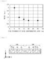
- FIG. 6 illustrates an example of the relationship between the film thickness (thickness t) of the oxide semiconductor layer 21 and noise.
- the horizontal axis in FIG. 6 represents the thickness (nm) of the oxide semiconductor layer 21.
- the vertical axis represents noise (a.u.).
- the oxide semiconductor layer 21 of 20 nm or more in thickness hardly generates noise. Assuming this noise generation is set at "1", the effect of noise is ignorable when it is 1.5 times or less.
- the solid-state imaging device 1 of the first embodiment includes the oxide semiconductor layer 21 that has thickness t set at 10 nm or more.
- FIGs. 7 to 12 illustrate the manufacturing method of the solid-state imaging device 1 according to the first embodiment, process by process.
- the following mainly describes the method of manufacturing the second photoelectric converter 20, while omitting the method of manufacturing the first photoelectric converter 3.
- the insulating film 24 is formed on the storage electrodes 25 in the region where the pixels 100 are to be formed.
- the insulating film 24 is also formed on the readout electrodes 26, but this insulating film 24 is removed to form openings. These openings are used for coupling the read electrode 26 to the corresponding feedthrough wiring 200. Note that the storage electrodes 25 and the readout electrodes 26 are formed above the first surface 2A of the substrate 2.
- the oxide semiconductor layer 21 of the second photoelectric converter 20 is formed on the insulating film 24.
- the oxide semiconductor layer 21 is coupled to the read electrodes 26 through the openings described above.
- the separation groove 281 is formed in the oxide semiconductor layer 21 between the regions where the pixels 100 are to be formed.
- a mask prepared by a photolithography technique and an anisotropic etching method such as reactive ion etching (RIE) are used, for example.
- the insulating film 282 is formed on the oxide semiconductor layer 21.
- the insulating film 282 is formed by a chemical vapor deposition (CVD) method, for example.
- the insulating film 282 formed is embedded in the separation groove 281.
- excess insulating film 282 on the oxide semiconductor layer 21 is removed, and a portion of the surface of the oxide semiconductor layer 21 is further removed to planarize the surface of the oxide semiconductor layer 21.
- CMP chemical mechanical polishing
- the etch-back method is also used for the planarization.
- the planarization forms the insulating separator 28 in the oxide semiconductor layer 21 between the regions where the pixels 100 are to be formed, and the insulating separator 28 includes the separation groove 281 and the insulating film 282.
- the oxide semiconductor layer 21 is formed to have a thickness t of 10 nm or more, for example (see FIG. 6 ).
- the oxide semiconductor layer 21 is formed to have a thickness t such that the electron density in the region D adjacent to the surface of the oxide semiconductor layer 21 is 1 ⁇ 10 17 cm 3 or less, for example, during the operation (see FIG. 5 ).
- the oxide layer 210 is formed on the oxide semiconductor layer 21.
- the photoelectric conversion layer 22 is subsequently formed on the oxide layer 210, and the transparent electrode 23 is formed on the photoelectric conversion layer 22, as illustrated in FIG. 3 described above.
- the sealing film 30, the second filter 31, the planarizing film 32, and the optical lens 33 are formed in sequence.
- the solid-state imaging device 1 according to the first embodiment is completed and the manufacturing method is finished.
- the solid-state imaging device 1 includes the oxide semiconductor layer 21 and the photoelectric conversion layer 22.
- the oxide semiconductor layer 21 is disposed above the substrate 2.
- the photoelectric conversion layer 22 is stacked on the oxide semiconductor layer 21 on the opposite side of the substrate 2.
- the solid-state imaging device 1 further includes the insulating separator 28.
- the insulating separator 28 is disposed in the oxide semiconductor layer 21 between the pixels 100 and includes an insulator.
- the insulating separator 28 is able to physically block the dark current flowing from a pixel 100 to the adjacent pixel 100 through the oxide semiconductor layer 21. This makes it possible to effectively suppress or prevent dark current, which is the cause of noise.
- the position of the surface of the insulating separator 28 on a side of the photoelectric conversion layer 22 is the same as the position of the surface of the oxide semiconductor layer 21 on a side of the photoelectric conversion layer 22.
- This configuration is able to reliably intercept the dark current flowing through the oxide semiconductor layer 21 because the insulating separator 28 is disposed in the entire thickness direction of the oxide semiconductor layer 21.
- the oxide semiconductor layer 21 in the solid-state imaging device 1 includes IGZO, IGSiO, or IAZO. That is, any of the materials is able to effectively suppress or prevent dark current flowing through the oxide semiconductor layer 21.
- the insulating separator 28 in the solid-state imaging device 1 includes SiO 2 .
- the insulating film 282 of the insulating separator 28 includes SiO 2 .
- the insulating separator 28 has electrical insulation properties and is also able to repair oxygen defects in the oxide semiconductor layer 21, thus making it possible to effectively suppress or prevent the dark current flowing through the oxide semiconductor layer 21, and improve the charge transfer efficiency.
- the insulating separator 28 includes one or more insulating materials selected from SiON, AlO, TiO, and TiSiO. This makes it possible to effectively suppress or prevent dark current flowing through the oxide semiconductor layer 21, and also improve the sealing performance.
- the oxide semiconductor layer 21 in the solid-state imaging device 1 is formed to have a thickness t such that the electron density is 1 ⁇ 10 17 cm 3 or less during the operation.
- the oxide semiconductor layer 21 in the solid-state imaging device 1 is formed to have a thickness t of 10 nm or more.
- the method of manufacturing the solid-state imaging device 1 according to the first embodiment has the following processes.
- the oxide semiconductor layer 21 is formed above the substrate 2.
- the separation groove 281 is formed between the regions where the pixels 100 are to be formed, and the separation groove 281 is formed in the thickness direction from the surface of the oxide semiconductor layer 21 on the opposite side of the substrate 2.
- the insulating film 282 is embedded in the separation groove 281 to form the insulating separator 28.
- the photoelectric conversion layer 22 is formed on the surface of the oxide semiconductor layer 21.
- the insulating film 282 on the surface of the oxide semiconductor layer 21 is removed, and a portion of the oxide semiconductor layer 21 is removed from the surface in the thickness direction.
- the oxide semiconductor layer 21 is formed to have a thickness t such that an electron density is 1 ⁇ 10 17 cm 3 or less during the operation.
- the insulating film 282 on the surface of the oxide semiconductor layer 21 is removed, and a portion of the oxide semiconductor layer 21 is removed from the surface in the thickness direction.
- the oxide semiconductor layer 21 is formed to have a thickness t of 10 nm or more.
- the same or substantially the same components as those of the solid-state imaging device 1 according to the first embodiment are denoted by the same reference numerals, and duplicate explanations will be omitted.
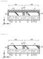
- FIG. 13 illustrates an example of the specific cross-sectional configuration of pixels 100.
- the surface of the insulating separator 28 on a side of the photoelectric conversion layer 22 is located closer to the photoelectric conversion layer 22 than the surface of the oxide semiconductor layer 21 on a side of the photoelectric conversion layer 22.
- the insulating separator 28 is disposed across the oxide semiconductor layer 21 and the oxide layer 210. That is, the position of the surface of the insulating separator 28 on a side of the photoelectric conversion layer 22 is the same as the position of the surface of the oxide layer 210 on a side of the photoelectric conversion layer 22.
- the components other than the above are the same as those of the solid-state imaging device 1 according to the first embodiment.
- FIGs. 14 to 17 illustrate the manufacturing method of the solid-state imaging device 1 according to the second embodiment, process by process.
- the oxide layer 210 is formed on the oxide semiconductor layer 21.
- the separation groove 281 is formed in the oxide layer 210 and the oxide semiconductor layer 21 between the regions where the pixels 100 are to be formed.
- the insulating film 282 is formed on the oxide layer 210.
- the insulating film 282 formed is embedded in the separation groove 281.
- excess insulating film 282 on the oxide layer 210 is removed.
- the insulating separator 28 with the separation groove 281 and insulating film 282 is formed.
- the photoelectric conversion layer 22 is subsequently formed on the oxide layer 210, and the transparent electrode 23 is formed on the photoelectric conversion layer 22, as illustrated in FIG. 13 described above.
- the sealing film 30, the second filter 31, the planarizing film 32, and the optical lens 33 are formed in sequence.
- the solid-state imaging device 1 according to the second embodiment is completed and the manufacturing method is finished.
- the same workings and effects are obtainable as those obtained from the solid-state imaging device 1 and the method of manufacturing the solid-state imaging device 1 according to the first embodiment.
- the surface of the insulating separator 28 on a side of the photoelectric conversion layer 22 is located closer to the photoelectric conversion layer 22 than the surface of the oxide semiconductor layer 21 on a side of the photoelectric conversion layer 22.
- This configuration is able to more reliably intercept the dark current flowing through the oxide semiconductor layer 21 because the insulating separator 28 is disposed in the entire thickness direction of the oxide semiconductor layer 21 and the oxide layer 210.
- FIG. 18 the following describes a solid-state imaging device 1 according to the third embodiment of the present disclosure.
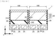
- FIG. 18 illustrates an example of the specific cross-sectional configuration of pixels 100.
- the surface of the insulating separator 28 on a side of the photoelectric conversion layer 22 is located closer to the photoelectric conversion layer 22 than the surface of the oxide semiconductor layer 21 on a side of the photoelectric conversion layer 22.
- the insulating separator 28 is disposed across the oxide semiconductor layer 21, the oxide layer 210, the photoelectric conversion layer 22, and the transparent electrode 23.
- the position of the surface of the insulating separator 28 on a side of the photoelectric conversion layer 22 is the same as the position of the surface of the transparent electrode 23 on a side of the optical lens 33.
- the insulating separator 28 is formed.
- the components other than the above are the same as those of the solid-state imaging device 1 according to the first embodiment.
- the present technology is not limited to the embodiments described above, and is modifiable in various ways without departing from the gist thereof.
- the oxide layer between the oxide semiconductor layer and the photoelectric conversion layer of the second photoelectric converter may be omitted in the solid-state imaging devices of the first to third embodiments described above.
- the solid-state imaging device includes the oxide semiconductor layer and the photoelectric conversion layer.
- the oxide semiconductor layer is disposed above the substrate.
- the photoelectric conversion layer is stacked on the oxide semiconductor layer on the opposite side of the substrate.
- the solid-state imaging device further includes the insulating separator.
- the insulation separator is disposed in the oxide semiconductor layer between the pixels and includes an insulator.
- the insulating separator is able to physically block the dark current flowing from a pixel to the adjacent pixel through the oxide semiconductor. This makes it possible to effectively suppress or prevent dark current, which is the cause of noise.
- the method of manufacturing the solid-state imaging device includes forming the oxide semiconductor layer above the substrate. Next, the separation groove is formed between the regions where the pixels are to be formed, and the separation groove is formed in the thickness direction from the surface of the oxide semiconductor layer on the opposite side of the substrate. Next, the insulating film is embedded in the separation groove to form the insulating separator. The photoelectric conversion layer is formed on the surface of the oxide semiconductor layer.
- the present technology has the following configuration.
- the following configuration makes it possible to provide a solid-state imaging device and a method of manufacturing the solid-state imaging device that is able to effectively suppress or prevent dark current, which causes the noise.
Landscapes
- Solid State Image Pick-Up Elements (AREA)
Abstract
Description
- The present disclosure relates to a solid-state imaging device and a method of manufacturing the solid-state imaging device.
-
PTL 1 discloses an imaging element, a stacked imaging element, and a solid-state imaging device. The imaging element includes a first electrode, a photoelectric conversion layer including an organic material, and a second electrode. This imaging element has an oxide semiconductor layer formed between the first electrode and the photoelectric conversion layer. - PTL 1: International Publication No.
WO2020/017330 - For the imaging element described above, it is desired to effectively suppress or prevent dark current flowing through the oxide semiconductor layer in a region corresponding between pixels.
- A solid-state imaging device according to a first embodiment of the present disclosure includes: an oxide semiconductor layer disposed above a substrate; a photoelectric conversion layer stacked on the oxide semiconductor layer on an opposite side of the substrate; and an insulating separator disposed in the oxide semiconductor layer between pixels, the insulation separator including an insulator.
- A method of manufacturing a solid-state imaging device according to a second embodiment of the present disclosure includes: forming an oxide semiconductor layer above a substrate; forming a separation groove between regions where pixels are to be formed, the separation groove being formed in a thickness direction of the oxide semiconductor layer from a surface of the oxide semiconductor layer on an opposite side of the substrate; forming an insulating separator by embedding an insulating film in the separation groove; and forming a photoelectric conversion layer on the surface.
-
- [
FIG. 1] FIG. 1 is a diagram illustrating a vertical cross-sectional configuration of a portion of a pixel of a solid-state imaging device according to a first embodiment of the present disclosure. - [
FIG. 2] FIG. 2 is a diagram illustrating a planar configuration of the pixel inFIG. 1 ; - [
FIG. 3] FIG. 3 is a diagram illustrating a vertical cross-sectional view of the main part of the pixel inFIG. 2 (cross-sectional view taken along the A-A line inFIG. 2 ). - [
FIG. 4] FIG. 4 is a graph to describe workings and effects of the solid-state imaging device according to the first embodiment, compared to the solid-state imaging device according to the comparative example. - [
FIG. 5] FIG. 5 is a conceptual diagram corresponding toFIG 3 , which explains workings and effects of the solid-state imaging device according to the first embodiment. - [
FIG. 6] FIG. 6 is a graph illustrating the relationship between the thickness of the oxide semiconductor layer and noise, which explains workings and effects of the solid-state imaging device according to the first embodiment. - [
FIG. 7] FIG. 7 is a cross-sectional view of a first process corresponding toFIG. 3 , which explains the method of manufacturing the solid-state imaging device according to the first embodiment. - [
FIG. 8] FIG. 8 is a cross-sectional view of a second process. - [
FIG. 9] FIG. 9 is a cross-sectional view of a third process. - [
FIG. 10] FIG. 10 is a cross-sectional view of a fourth process. - [
FIG. 11] FIG. 11 is a cross-sectional view of a fifth process. - [
FIG. 12] FIG. 12 is a cross-sectional view of a sixth process. - [
FIG. 13] FIG. 13 is a diagram illustrating a vertical cross-sectional configuration of the main part of a pixel of a solid-state imaging device according to a second embodiment of the present disclosure, corresponding toFIG. 3 . - [
FIG. 14] FIG. 14 is a cross-sectional view of a first process corresponding toFIG. 3 , which explains the method of manufacturing the solid-state imaging device according to the second embodiment. - [
FIG. 15] FIG. 15 is a cross-sectional view of a second process. - [
FIG. 16] FIG. 16 is a cross-sectional view of a third process. - [
FIG. 17] FIG. 17 is a cross-sectional view of a fourth process. - [
FIG. 18] FIG. 18 is a diagram illustrating a vertical cross-sectional configuration of the main part of a pixel of a solid-state imaging device according to a third embodiment of the present disclosure, corresponding toFIG. 3 . - The following describes embodiments of the present disclosure in details with reference to the drawings. Note that the explanation will be given in the following order.
- The first embodiment describes an example of applying the present technology to a solid-state imaging device. The first embodiment describes a vertical cross-sectional configuration and a planar configuration of the solid-state imaging device. The first embodiment then describes a method of manufacturing the solid-state imaging device.
- The second embodiment describes a first example of changing the configuration of the insulating separator of the solid-state imaging device according to the first embodiment. The second embodiment then describes a method of manufacturing the solid-state imaging device.
- The third embodiment describes a second example of changing the configuration of the insulating separator of the solid-state imaging device according to the first embodiment.
- Referring to
FIGs. 1 to 12 , the following describes a solid-state imaging device 1 according to the first embodiment of the present disclosure and a method of manufacturing the solid-state imaging device 1. - Here, the direction of arrow X in the drawings illustrated as appropriate indicates one planar direction of the solid-
state imaging device 1 placed on a plane for convenience. The direction of arrow Y indicates another plane direction orthogonal to the arrow X direction. The direction of arrow Z indicates upward direction orthogonal to the arrow X direction and arrow Y direction. That is, the arrow X direction, arrow Y direction, and arrow Z direction exactly coincide with the X-axis direction, Y-axis direction, and Z-axis direction, respectively, of the three-dimensional coordinate system. - Note that these directions are illustrated to help understand the explanation, and do not limit the directions of the present technology.
-
FIG. 1 illustrates an example of a vertical cross-sectional configuration of apixel 100 of a solid-state imaging device 1. - The solid-
state imaging device 1 according to the first embodiment is able to acquire visible-light information and distance information using acommon pixel 100. The solid-state imaging device 1 includes asubstrate 2, a firstphotoelectric converter 3, and a secondphotoelectric converter 20. The solid-state imaging device 1 further includes afirst filter 10, asecond filter 31, and anoptical lens 33. - Letting that the arrow Z direction is the thickness direction, the
substrate 2 has a first surface (top surface) 2A that extends in the arrow X and arrow Y directions, and a second surface (bottom surface) 2B facing thefirst surface 2A. Light enters from thefirst surface 2A. - For instance, the
substrate 2 used is a semiconductor substrate including single crystal silicon (Si). Although not clearly illustrated, a p-type well region of a first conductivity type is formed in the semiconductor substrate. - A first
photoelectric converter 3 is formed in thesubstrate 2 at the region corresponding to asingle pixel 100. The firstphotoelectric converter 3 converts light into electric charge. - Although a detailed description of the configuration is omitted, the first
photoelectric converter 3 includes a photodiode. The photodiode is formed at a pn junction between an n-type semiconductor region and a p-type semiconductor region. For instance, the firstphotoelectric converter 3 in this embodiment is configured to be sensitive to all visible light from blue light to red light. - The first
photoelectric converter 3 is coupled to awiring 7 with a transfer transistor 4 interposed therebetween, the transfer transistor 4 being disposed on thesecond surface 2B of thesubstrate 2. - The transfer transistor 4 includes a
gate electrode 41 and a pair of main electrodes. Note here that the transfer transistor 4 includes an n-channel insulated gate field effect transistor (IGFET). IGFET refers to both a metal insulator semiconductor field effect transistor (MISFET) and a metal oxide semiconductor field effect transistor (MOSFET). - One of the main electrodes of the transfer transistor 4 includes the photodiode of the first
photoelectric converter 3. The other main electrode includes a floatingelectrode 42 disposed on thesecond surface 2B of thesubstrate 2. The floatingelectrode 42 in this embodiment includes an n-type semiconductor region (n-type diffusion region). - The transfer transistor 4 transfers the electric charge converted from light at the first
photoelectric converter 3 to the floatingelectrode 42 in accordance with a control signal applied to thegate electrode 41. - The
wiring 7 is disposed below thesecond surface 2B of thesubstrate 2 with an insulatinglayer 5 interposed therebetween. Thewiring 7 is electrically coupled to the floatingelectrode 42 through aconnection hole wiring 6 that penetrates the insulatinglayer 5 in the thickness direction. - For instance, the
wiring 7 includes copper (Cu). For instance, theconnection hole wiring 6 includes a conductive metal material such as tungsten (W). - Note here that, although not illustrated in
FIG. 1 , a circuit for constituting an indirect time of flight (iToF) sensor is disposed at thesecond surface 2B of thesubstrate 2. An iToF sensor accumulates incident light and detects the phase difference between the incident light and the emitted light, thus making it possible to measure a distance. - The
first filter 10 is disposed above thefirst surface 2A of thesubstrate 2 with a fixedcharge layer 8 interposed therebetween. Thefirst filter 10 is disposed in an insulatinglayer 9 formed on thefirst surface 2A of thesubstrate 2. Thefirst filter 10 in this embodiment is configured to block visible light and transmit infrared light. That is, when using infrared light at thesubstrate 2, thefirst filter 10 is able to reduce color mixing between the infrared light and ultraviolet light. - The
first filter 10 may be configured to block visible light and transmit blue light. That is, when using blue light at thesubstrate 2, thefirst filter 10 is able to reduce color mixing between the blue light and ultraviolet light. - The fixed
charge layer 8 is disposed between thefirst surface 2A of thesubstrate 2 and the insulatinglayer 9. In this embodiment, viewed in the arrow Y direction (hereinafter simply referred to as "in lateral view"), the fixedcharge layer 8 has a cross-sectional shape that alternates between protruding toward the light-entering side and protruding toward the opposite side of the light-entering in the arrow X direction. In other words, the fixedcharge layer 8 has a zigzag shape in cross section. A negative charge is applied to the fixedcharge layer 8. - The fixed
charge layer 8 configured in this way is able to confine infrared light, for example, within thesubstrate 2. Alternatively, the fixedcharge layer 8 is able to blue light, for example, within thesubstrate 2. - Note that between the
pixels 100, an inter-pixellight shielding layer 11 is disposed between thefirst filter 10 and the fixedcharge layer 8. The inter-pixellight shielding layer 11 is able to reduce color mixing of light between thepixel 100 andother pixels 100 adjacent thereto. - The second
photoelectric converter 20 is opposed to the firstphotoelectric converter 3 with thefirst filter 10 interposed therebetween. The secondphotoelectric converter 20 includes anoxide semiconductor layer 21, aphotoelectric conversion layer 22, and atransparent electrode 23. - The
oxide semiconductor layer 21 is opposed to thefirst surface 2A of thesubstrate 2. Specifically, theoxide semiconductor layer 21 is opposed to thefirst filter 10 with astorage electrode 25 and an insulatingfilm 24 interposed therebetween. - The
oxide semiconductor layer 21 is transparent semiconductor that transmits electromagnetic waves in the visible light range, and accumulates electrons converted from light at thephotoelectric conversion layer 22. Theoxide semiconductor layer 21 includes IGZO containing indium (In), gallium (Ga), zinc (Zn), and oxygen (O), for example. Theoxide semiconductor layer 21 may include IGSiO containing In, Ga, Si, and O and IAZO containing In, aluminum (Al), Zn, and O. - For instance, the
oxide semiconductor layer 21 has a thickness of 10 nm or more and 100 nm or less. - The
photoelectric conversion layer 22 is stacked on theoxide semiconductor layer 21. Thephotoelectric conversion layer 22 includes a photoelectric conversion material that is sensitive to green light, for example. This photoelectric conversion material includes an organic photoelectric conversion material such as rhodamine dyes, merocyanine dyes, or quinacridone. - For instance, the
photoelectric conversion layer 22 has a thickness of 100 nm or more and 1000 nm or less. - The
transparent electrode 23 is stacked on thephotoelectric conversion layer 22. Thetransparent electrode 23 includes indium oxide-zinc oxide series oxide (IZO), for example. Thetransparent electrode 23 may also include indium tin oxide (ITO). - For instance, the
transparent electrode 23 has a thickness of 10 nm or more and 100 nm or less. - The
storage electrode 25 stores the electric charge, which is converted from light at the secondphotoelectric converter 20, in theoxide semiconductor layer 21. The stored electric charge is read out by areadout electrode 26. Thestorage electrode 25 is disposed between thefirst filter 10 and theoxide semiconductor layer 21. The insulatingfilm 24 is disposed between thestorage electrode 25 and theoxide semiconductor layer 21. Similar to thetransparent electrode 23, thestorage electrode 25 includes a transparent electrode material, for example. The insulatingfilm 24 operates as a gate insulating film. In other words, thestorage electrode 25, insulatingfilm 24, andoxide semiconductor layer 21 constitute a metal-insulator-semiconductor type capacitance. - The
readout electrode 26 is disposed in the same layer as thestorage electrode 25. When a control signal is applied to thereadout electrode 26, thereadout electrode 26 transfers the electric charge accumulated in the circuit disposed at thesecond surface 2B of thesubstrate 2 through afeedthrough wiring 200. Thefeedthrough wiring 200 penetrates thesubstrate 2 in the thickness direction. - A
light shielding wall 201 is also disposed between thesubstrate 2 and thefeedthrough wiring 200 to cover the periphery of the lateral surface of thefeedthrough wiring 200. Thelight shielding wall 201 is able to reduce color mixing. - The
second filter 31 is opposed to the secondphotoelectric converter 20 on the opposite side of thefirst filter 10 with a sealingfilm 30 interposed therebetween. Thesecond filter 31 is able to transmit visible light including red light, green light, and blue light, for example. The sealingfilm 30 includes an insulating film containing Al and titanium (Ti) or an insulating film such as silicon nitride (SiN), for example. - Note that the
second filter 31 is not necessary for the solid-state imaging device 1 that detects only black and white incident light. - The
optical lens 33 is opposed to thesecond filter 31 on the opposite side of the secondphotoelectric converter 20 with aplanarizing film 32 interposed therebetween. Theoptical lens 33 in this embodiment includes an on-chip lens. -
FIG. 2 illustrates an example of the specific planar configuration ofpixels 100.FIG. 3 illustrates an example of the specific cross-sectional configuration ofpixels 100. - One
pixel 100 has a rectangular shape, viewed in the direction of arrow Z (hereinafter simply referred to as "plan view"). In this example, thepixel 100 has a square shape. In plan view, thepixels 100 are regularly arranged at the equal intervals in each of the arrow X direction and the arrow Y direction. That is, thepixels 100 are arranged in a matrix shape. - In a region surrounded by the inter-pixel
light shielding layer 11, the secondphotoelectric converter 20 is disposed over almost the entire region of thepixel 100. In this embodiment, twostorage electrodes 25 are disposed in each of the arrow X direction and the arrow Y direction, that is, a total of fourstorage electrodes 25 is disposed. - One
readout electrode 26 is disposed in the middle of thestorage electrodes 25 arranged that are four in total (at the middle of the pixels 100). - As illustrated in
FIG. 3 as lateral view, the secondphotoelectric converter 20 includes anoxide layer 210 disposed between theoxide semiconductor layer 21 and thephotoelectric conversion layer 22. Theoxide layer 210 makes it possible to improve oxygen deficiency near the surface of theoxide semiconductor layer 21 and improve the transfer characteristics of electric charge. - Although the detailed configuration is omitted, the
oxide layer 210 includes a film stack of a metal oxide film and a tunnel oxide film. - The metal oxide film includes at least one element selected from tantalum (Ta), Ti, palladium (Pd), niobium (Nb), tungsten (W), zirconium (Zr), hafnium (Hf), scandium (Sc), yttrium (Y), lanthanum. (La), gallium (Ga), and manganese (Mg).
- The tunnel oxide film includes at least one material selected from SiOx, SiON, SiOC, and AlOY.
- The
oxide layer 210 also includes at least one element added, which is selected from Si, Ta, Pd, Nb, W, Zr, Hf, Sc, Y, La, Ga, Mg, aluminum (Al), strontium (Sr), germanium (Ge), hydrogen (H2), carbon (C), and nitrogen (N2). - For instance, the
oxide layer 210 has a thickness of 0.2 nm or more (approximately one atomic layer or more) and 10 nm or less. - As illustrated in
FIGs. 2 and 3 , the solid-state imaging device 1 of the first embodiment includes the insulatingseparator 28 disposed in theoxide semiconductor layer 21 of the secondphotoelectric converter 20 between thepixels 100. - Specifically, the insulating
separator 28 surrounds apixel 100 in plan view. The insulatingseparator 28 also surrounds at least the lateral periphery of theoxide semiconductor layer 21 in lateral view. - The insulating
separator 28 includes aseparation groove 281 and an insulatingfilm 282. - The
separation groove 281 penetrates from the top surface of theoxide semiconductor layer 21 on a side of thesecond filter 31 to the bottom surface on a side of thefirst filter 10. In this embodiment, theseparation groove 281 has a constant width. - Note that the
separation groove 281 may have a tapered shape, a stepped shape, and other shapes that are different in width between the top surface and the bottom surface of theoxide semiconductor layer 21. - The insulating
film 282 is embedded in theseparation groove 281. In the first embodiment, the insulatingfilm 282 includes silicon oxide (SiO2), for example. SiO2 has electrical insulating properties and further is able to repair oxygen defects in theoxide semiconductor layer 21. - That is, the insulating
separator 28 is able to block the flow of electric charge, specifically the flow of dark current, which causes noise betweenadjacent pixels 100. In addition, the insulatingseparator 28 is able to repair oxygen defects in theoxide semiconductor layer 21 of the secondphotoelectric converter 20, thus making it possible to improve the transfer efficiency of electric charge. - The insulating
film 282 of the insulatingseparator 28 may also include one or more insulating materials selected from silicon oxynitride (SiON), aluminum oxide (AlO), titanium oxide (TiO), and titanium oxide silicide (TiSiO). These insulating materials are able to effectively inhibit the ingress of H2, thus making it possible to improve sealing performance. -
FIG. 4 is an example graph representing noise characteristics. - Letter A on the horizontal axis in
FIG. 4 indicates the noise characteristics of the solid-state imaging device 1 according to the first embodiment. Letter B indicates the noise characteristics of a solid-state imaging device according to a comparative example. The vertical axis represents noise (a.u.). - The solid-
state imaging device 1 of the first embodiment includes the insulatingseparator 28 in theoxide semiconductor layer 21 of the secondphotoelectric converter 20 between thepixels 100. This makes it possible to significantly reduce noise compared to the solid-state imaging device of the comparative example. -
FIG. 5 illustrates a specific cross-sectional configuration of apixel 100, conceptually illustrating the state of electron density. - In the region indicated by letter C in
FIG. 5 , that is, adjacent to thestorage electrode 25 of theoxide semiconductor layer 21, the electron density is 1×1019 cm3, for example, upon operations including charge storage and charge transfer operations. - In the region indicated by letter D, that is, adjacent to the
photoelectric conversion layer 22 of theoxide semiconductor layer 21, the electron density is 1×1017 cm3 or less, for example, upon operations. The solid-state imaging device 1 of the first embodiment includes theoxide semiconductor layer 21 that is formed to have a thickness t, at which the electron density in region D is the above-described value or less. The electron density of the above-described value or less makes it possible to effectively suppress noise. -
FIG. 6 illustrates an example of the relationship between the film thickness (thickness t) of theoxide semiconductor layer 21 and noise. The horizontal axis inFIG. 6 represents the thickness (nm) of theoxide semiconductor layer 21. The vertical axis represents noise (a.u.). - As illustrated in
FIG. 6 , theoxide semiconductor layer 21 of 20 nm or more in thickness hardly generates noise. Assuming this noise generation is set at "1", the effect of noise is ignorable when it is 1.5 times or less. Thus, the solid-state imaging device 1 of the first embodiment includes theoxide semiconductor layer 21 that has thickness t set at 10 nm or more. -
FIGs. 7 to 12 illustrate the manufacturing method of the solid-state imaging device 1 according to the first embodiment, process by process. The following mainly describes the method of manufacturing the secondphotoelectric converter 20, while omitting the method of manufacturing the firstphotoelectric converter 3. - As illustrated in
FIG. 7 , the insulatingfilm 24 is formed on thestorage electrodes 25 in the region where thepixels 100 are to be formed. The insulatingfilm 24 is also formed on thereadout electrodes 26, but this insulatingfilm 24 is removed to form openings. These openings are used for coupling theread electrode 26 to the correspondingfeedthrough wiring 200. Note that thestorage electrodes 25 and thereadout electrodes 26 are formed above thefirst surface 2A of thesubstrate 2. - As illustrated in
FIG. 8 , theoxide semiconductor layer 21 of the secondphotoelectric converter 20 is formed on the insulatingfilm 24. Theoxide semiconductor layer 21 is coupled to the readelectrodes 26 through the openings described above. - As illustrated in
FIG. 9 , theseparation groove 281 is formed in theoxide semiconductor layer 21 between the regions where thepixels 100 are to be formed. To form theseparation groove 281, a mask prepared by a photolithography technique and an anisotropic etching method such as reactive ion etching (RIE) are used, for example. - As illustrated in
FIG. 10 , the insulatingfilm 282 is formed on theoxide semiconductor layer 21. The insulatingfilm 282 is formed by a chemical vapor deposition (CVD) method, for example. The insulatingfilm 282 formed is embedded in theseparation groove 281. - As illustrated in
FIG. 11 , excess insulatingfilm 282 on theoxide semiconductor layer 21 is removed, and a portion of the surface of theoxide semiconductor layer 21 is further removed to planarize the surface of theoxide semiconductor layer 21. For planarization, a chemical mechanical polishing (CMP) method is used, for example. The etch-back method is also used for the planarization. - The planarization forms the insulating
separator 28 in theoxide semiconductor layer 21 between the regions where thepixels 100 are to be formed, and the insulatingseparator 28 includes theseparation groove 281 and the insulatingfilm 282. - In this process, damage occurs on the surface of the
oxide semiconductor layer 21 due to the CMP method or the etch-back method. Thus, theoxide semiconductor layer 21 is formed to have a thickness t of 10 nm or more, for example (seeFIG. 6 ). In addition, theoxide semiconductor layer 21 is formed to have a thickness t such that the electron density in the region D adjacent to the surface of theoxide semiconductor layer 21 is 1×1017 cm3 or less, for example, during the operation (seeFIG. 5 ). - As illustrated in
FIG. 12 , theoxide layer 210 is formed on theoxide semiconductor layer 21. - The
photoelectric conversion layer 22 is subsequently formed on theoxide layer 210, and thetransparent electrode 23 is formed on thephotoelectric conversion layer 22, as illustrated inFIG. 3 described above. - Thereafter, as illustrated in
FIG. 1 described above, the sealingfilm 30, thesecond filter 31, theplanarizing film 32, and theoptical lens 33 are formed in sequence. - When a series of these manufacturing processes ends, the solid-
state imaging device 1 according to the first embodiment is completed and the manufacturing method is finished. - As illustrated in
FIGs. 1 to 3 , the solid-state imaging device 1 according to the first embodiment includes theoxide semiconductor layer 21 and thephotoelectric conversion layer 22. Theoxide semiconductor layer 21 is disposed above thesubstrate 2. Thephotoelectric conversion layer 22 is stacked on theoxide semiconductor layer 21 on the opposite side of thesubstrate 2. - In this embodiment, the solid-
state imaging device 1 further includes the insulatingseparator 28. The insulatingseparator 28 is disposed in theoxide semiconductor layer 21 between thepixels 100 and includes an insulator. - With this configuration, as illustrated in
FIG. 4 , the insulatingseparator 28 is able to physically block the dark current flowing from apixel 100 to theadjacent pixel 100 through theoxide semiconductor layer 21. This makes it possible to effectively suppress or prevent dark current, which is the cause of noise. - As illustrated in
FIG. 3 , in the solid-state imaging device 1, the position of the surface of the insulatingseparator 28 on a side of thephotoelectric conversion layer 22 is the same as the position of the surface of theoxide semiconductor layer 21 on a side of thephotoelectric conversion layer 22. - This configuration is able to reliably intercept the dark current flowing through the
oxide semiconductor layer 21 because the insulatingseparator 28 is disposed in the entire thickness direction of theoxide semiconductor layer 21. - In addition, as illustrated in
FIGs. 1 and3 , theoxide semiconductor layer 21 in the solid-state imaging device 1 includes IGZO, IGSiO, or IAZO. That is, any of the materials is able to effectively suppress or prevent dark current flowing through theoxide semiconductor layer 21. - In addition, as illustrated in
FIGs. 1 and3 , the insulatingseparator 28 in the solid-state imaging device 1 includes SiO2. In other words, the insulatingfilm 282 of the insulatingseparator 28 includes SiO2. - This means that the insulating
separator 28 has electrical insulation properties and is also able to repair oxygen defects in theoxide semiconductor layer 21, thus making it possible to effectively suppress or prevent the dark current flowing through theoxide semiconductor layer 21, and improve the charge transfer efficiency. - In addition, the insulating
separator 28 includes one or more insulating materials selected from SiON, AlO, TiO, and TiSiO. This makes it possible to effectively suppress or prevent dark current flowing through theoxide semiconductor layer 21, and also improve the sealing performance. - In addition, as illustrated in
FIG. 5 , theoxide semiconductor layer 21 in the solid-state imaging device 1 is formed to have a thickness t such that the electron density is 1×1017 cm3 or less during the operation. In addition, as illustrated inFIG. 6 , theoxide semiconductor layer 21 in the solid-state imaging device 1 is formed to have a thickness t of 10 nm or more. - This makes it possible to effectively suppress noise in the
oxide semiconductor layer 21. - The method of manufacturing the solid-
state imaging device 1 according to the first embodiment has the following processes. - As illustrated in
FIG. 8 , theoxide semiconductor layer 21 is formed above thesubstrate 2. As illustrated inFIG. 9 , theseparation groove 281 is formed between the regions where thepixels 100 are to be formed, and theseparation groove 281 is formed in the thickness direction from the surface of theoxide semiconductor layer 21 on the opposite side of thesubstrate 2. As illustrated inFIGs. 10 and 11 , the insulatingfilm 282 is embedded in theseparation groove 281 to form the insulatingseparator 28. As illustrated inFIG. 3 , thephotoelectric conversion layer 22 is formed on the surface of theoxide semiconductor layer 21. - With these processes, it is possible to easily form the insulating
separator 28 that is able to effectively suppress or prevent dark current flowing through theoxide semiconductor layer 21. - In the method of manufacturing the solid-
state imaging device 1, after forming the insulatingseparator 28, the insulatingfilm 282 on the surface of theoxide semiconductor layer 21 is removed, and a portion of theoxide semiconductor layer 21 is removed from the surface in the thickness direction. In this process, theoxide semiconductor layer 21 is formed to have a thickness t such that an electron density is 1×1017 cm3 or less during the operation. - Furthermore, in the method of manufacturing the solid-
state imaging device 1, after forming the insulatingseparator 28, the insulatingfilm 282 on the surface of theoxide semiconductor layer 21 is removed, and a portion of theoxide semiconductor layer 21 is removed from the surface in the thickness direction. In this process, theoxide semiconductor layer 21 is formed to have a thickness t of 10 nm or more. - With these processes, it is possible to easily form the
oxide semiconductor layer 21 that is able to effectively suppress noise. - Referring to
FIGs. 13 to 17 , the following describes a solid-state imaging device 1 according to the second embodiment of the present disclosure. - For the solid-
state imaging device 1 according to the second embodiment and subsequent embodiments, the same or substantially the same components as those of the solid-state imaging device 1 according to the first embodiment are denoted by the same reference numerals, and duplicate explanations will be omitted. -
FIG. 13 illustrates an example of the specific cross-sectional configuration ofpixels 100. - In the solid-
state imaging device 1 according to the second embodiment, the surface of the insulatingseparator 28 on a side of thephotoelectric conversion layer 22 is located closer to thephotoelectric conversion layer 22 than the surface of theoxide semiconductor layer 21 on a side of thephotoelectric conversion layer 22. In other words, the insulatingseparator 28 is disposed across theoxide semiconductor layer 21 and theoxide layer 210. That is, the position of the surface of the insulatingseparator 28 on a side of thephotoelectric conversion layer 22 is the same as the position of the surface of theoxide layer 210 on a side of thephotoelectric conversion layer 22. - The components other than the above are the same as those of the solid-
state imaging device 1 according to the first embodiment. -
FIGs. 14 to 17 illustrate the manufacturing method of the solid-state imaging device 1 according to the second embodiment, process by process. - As illustrated in
FIG. 14 , after forming theoxide semiconductor layer 21 inFIG. 8 illustrating the method of manufacturing the solid-state imaging device 1 according to the first embodiment (hereinafter simply referred to as "first manufacturing method"), theoxide layer 210 is formed on theoxide semiconductor layer 21. - As illustrated in
FIG. 15 , theseparation groove 281 is formed in theoxide layer 210 and theoxide semiconductor layer 21 between the regions where thepixels 100 are to be formed. - As illustrated in
FIG. 16 , the insulatingfilm 282 is formed on theoxide layer 210. The insulatingfilm 282 formed is embedded in theseparation groove 281. - As illustrated in
FIG. 17 , excess insulatingfilm 282 on theoxide layer 210 is removed. When the insulatingfilm 282 is removed, the insulatingseparator 28 with theseparation groove 281 and insulatingfilm 282 is formed. - The
photoelectric conversion layer 22 is subsequently formed on theoxide layer 210, and thetransparent electrode 23 is formed on thephotoelectric conversion layer 22, as illustrated inFIG. 13 described above. - Thereafter, as illustrated in
FIG. 1 described above, the sealingfilm 30, thesecond filter 31, theplanarizing film 32, and theoptical lens 33 are formed in sequence. - When a series of these manufacturing processes ends, the solid-
state imaging device 1 according to the second embodiment is completed and the manufacturing method is finished. - With the solid-
state imaging device 1 and the method of manufacturing the solid-state imaging device 1 according to the second embodiment, the same workings and effects are obtainable as those obtained from the solid-state imaging device 1 and the method of manufacturing the solid-state imaging device 1 according to the first embodiment. - As illustrated in
FIG. 13 , in the solid-state imaging device 1, the surface of the insulatingseparator 28 on a side of thephotoelectric conversion layer 22 is located closer to thephotoelectric conversion layer 22 than the surface of theoxide semiconductor layer 21 on a side of thephotoelectric conversion layer 22. - This configuration is able to more reliably intercept the dark current flowing through the
oxide semiconductor layer 21 because the insulatingseparator 28 is disposed in the entire thickness direction of theoxide semiconductor layer 21 and theoxide layer 210. - Referring to
FIG. 18 , the following describes a solid-state imaging device 1 according to the third embodiment of the present disclosure. -
FIG. 18 illustrates an example of the specific cross-sectional configuration ofpixels 100. - In the solid-
state imaging device 1 according to the third embodiment, the surface of the insulatingseparator 28 on a side of thephotoelectric conversion layer 22 is located closer to thephotoelectric conversion layer 22 than the surface of theoxide semiconductor layer 21 on a side of thephotoelectric conversion layer 22. In other words, the insulatingseparator 28 is disposed across theoxide semiconductor layer 21, theoxide layer 210, thephotoelectric conversion layer 22, and thetransparent electrode 23. The position of the surface of the insulatingseparator 28 on a side of thephotoelectric conversion layer 22 is the same as the position of the surface of thetransparent electrode 23 on a side of theoptical lens 33. - For the manufacturing method, after forming the
transparent electrode 23 by the first manufacturing method, the insulatingseparator 28 is formed. - The components other than the above are the same as those of the solid-
state imaging device 1 according to the first embodiment. - The present technology is not limited to the embodiments described above, and is modifiable in various ways without departing from the gist thereof.
- For instance, the oxide layer between the oxide semiconductor layer and the photoelectric conversion layer of the second photoelectric converter may be omitted in the solid-state imaging devices of the first to third embodiments described above.
- The solid-state imaging device according to the first embodiment of the present disclosure includes the oxide semiconductor layer and the photoelectric conversion layer. The oxide semiconductor layer is disposed above the substrate. The photoelectric conversion layer is stacked on the oxide semiconductor layer on the opposite side of the substrate.
- In this embodiment, the solid-state imaging device further includes the insulating separator. The insulation separator is disposed in the oxide semiconductor layer between the pixels and includes an insulator.
- With this configuration, the insulating separator is able to physically block the dark current flowing from a pixel to the adjacent pixel through the oxide semiconductor. This makes it possible to effectively suppress or prevent dark current, which is the cause of noise.
- The method of manufacturing the solid-state imaging device according to the second embodiment of the present disclosure includes forming the oxide semiconductor layer above the substrate. Next, the separation groove is formed between the regions where the pixels are to be formed, and the separation groove is formed in the thickness direction from the surface of the oxide semiconductor layer on the opposite side of the substrate. Next, the insulating film is embedded in the separation groove to form the insulating separator. The photoelectric conversion layer is formed on the surface of the oxide semiconductor layer.
- With these processes, it is possible to easily form the insulating separator that is able to effectively suppress or prevent dark current flowing through the oxide semiconductor.
- The present technology has the following configuration. The following configuration makes it possible to provide a solid-state imaging device and a method of manufacturing the solid-state imaging device that is able to effectively suppress or prevent dark current, which causes the noise.
- (1) A solid-state imaging device including:
- an oxide semiconductor layer disposed above a substrate;
- a photoelectric conversion layer stacked on the oxide semiconductor layer on an opposite side of the substrate; and
- an insulating separator disposed in the oxide semiconductor layer between pixels, the insulation separator including an insulator.
- (2) The solid-state imaging device according to (1), in which a position of a surface of the insulating separator on a side of the photoelectric conversion layer is the same as a position of a surface of the oxide semiconductor layer on a side of the photoelectric conversion layer.
- (3) The solid-state imaging device according to (1), in which a position of a surface of the insulating separator on a side of the photoelectric conversion layer is located closer to the photoelectric conversion layer than a position of a surface of the oxide semiconductor layer on a side of the photoelectric conversion layer.
- (4) The solid-state imaging device according to (1) or (3), further including a transparent electrode on the photoelectric conversion layer on an opposite side of the oxide semiconductor layer, in which
the insulating separator extends through the photoelectric conversion layer to the transparent electrode. - (5) The solid-state imaging device according to any one of (1) to (4), further including an oxide layer between the oxide semiconductor layer and the photoelectric conversion layer.
- (6) The solid-state imaging device according to (5), in which the oxide layer includes a film stack of a metal oxide film and a tunnel oxide film.
- (7) The solid-state imaging device according to (6), in which the metal oxide film includes at least one element selected from Ta, Ti, Pd, Nb, W, Zr, Hf, Sc, Y, La, Ga, and Mg.
- (8) The solid-state imaging device according to (5), in which the oxide film includes at least one element added, selected from Si, Ta, Pd, Nb, W, Zr, Hf, Sc, Y, La, Ga, Mg, Al, Sr, Ge, H2, C, and N2.
- (9) The solid-state imaging device according to any one of (1) to (8), in which the oxide semiconductor layer includes IGZO, IGSiO, or IAZO.
- (10) The solid-state imaging device according to any one of (1) to (9), in which the photoelectric conversion layer includes an organic photoelectric conversion layer.
- (11) The solid-state imaging device according to any one of (1) to (10), in which the insulating separator includes one or more materials selected from SiO2, SiON, AlO, TiO, and TiSiO.
- (12) The solid-state imaging device according to any one of (1) to (11), in which the oxide semiconductor layer has a thickness to allow an electron density to be 1×1017 cm3 or less upon operation.
- (13) The solid-state imaging device according to any one of (1) to (12), in which the oxide semiconductor layer has a thickness of 10 nm or more.
- (14) A method of manufacturing a solid-state imaging device, including:
- forming an oxide semiconductor layer above a substrate;
- forming a separation groove between regions where pixels are to be formed, the separation groove being formed in a thickness direction of the oxide semiconductor layer from a surface of the oxide semiconductor layer on an opposite side of the substrate;
- forming an insulating separator by embedding an insulating film in the separation groove; and
- forming a photoelectric conversion layer on the surface.
- (15) The method of manufacturing the solid-state imaging device according to (14), further including, after forming the insulating separator:
- removing the insulating film on the surface; and
- removing a part of the surface of the oxide semiconductor layer in the thickness direction to form the oxide semiconductor layer having a thickness to allow an electron density to be 1×1017 cm3 or less upon operation.
- (16) The method of manufacturing the solid-state imaging device according to (14) or (15), further including, after forming the insulation separator:
- removing the insulating film on the surface; and
- removing a part of the surface of the oxide semiconductor layer in the thickness direction to form the oxide semiconductor layer having a thickness of 10 nm or more.
- The present application claims the benefit of Japanese Priority Patent Application
JP2022-020874 filed with the Japan Patent Office on February, 14, 2022 - It should be understood by those skilled in the art that various modifications, combinations, sub-combinations and alterations may occur depending on design requirements and other factors insofar as they are within the scope of the appended claims or the equivalents thereof.
Claims (16)
- A solid-state imaging device comprising:an oxide semiconductor layer disposed above a substrate;a photoelectric conversion layer stacked on the oxide semiconductor layer on an opposite side of the substrate; andan insulating separator disposed in the oxide semiconductor layer between pixels, the insulation separator including an insulator.
- The solid-state imaging device according to claim 1, wherein a position of a surface of the insulating separator on a side of the photoelectric conversion layer is same as a position of a surface of the oxide semiconductor layer on a side of the photoelectric conversion layer.
- The solid-state imaging device according to claim 1, wherein a position of a surface of the insulating separator on a side of the photoelectric conversion layer is located closer to the photoelectric conversion layer than a position of a surface of the oxide semiconductor layer on a side of the photoelectric conversion layer.
- The solid-state imaging device according to claim 1, further comprising a transparent electrode on the photoelectric conversion layer on an opposite side of the oxide semiconductor layer, wherein
the insulating separator extends through the photoelectric conversion layer to the transparent electrode. - The solid-state imaging device according to claim 1, further comprising an oxide layer between the oxide semiconductor layer and the photoelectric conversion layer.
- The solid-state imaging device according to claim 5, wherein the oxide layer comprises a film stack of a metal oxide film and a tunnel oxide film.
- The solid-state imaging device according to claim 6, wherein the metal oxide film includes at least one element selected from Ta, Ti, Pd, Nb, W, Zr, Hf, Sc, Y, La, Ga, and Mg.
- The solid-state imaging device according to claim 5, in which the oxide layer includes at least one element added, selected from Si, Ta, Pd, Nb, W, Zr, Hf, Sc, Y, La, Ga, Mg, Al, Sr, Ge, H2, C, and N2.
- The solid-state imaging device according to claim 1, wherein the oxide semiconductor layer includes IGZO, IGSiO, or IAZO.
- The solid-state imaging device according to claim 1, wherein the photoelectric conversion layer comprises an organic photoelectric conversion layer.
- The solid-state imaging device according to claim 1, wherein the insulating separator includes one or more materials selected from SiO2, SiON, AlO, TiO, and TiSiO.
- The solid-state imaging device according to claim 1, wherein the oxide semiconductor layer has a thickness to allow an electron density to be 1×1017 cm3 or less upon operation.
- The solid-state imaging device according to claim 1, wherein the oxide semiconductor layer has a thickness of 10 nm or more.
- A method of manufacturing a solid-state imaging device, the method comprising:forming an oxide semiconductor layer above a substrate;forming a separation groove between regions where pixels are to be formed, the separation groove being formed in a thickness direction of the oxide semiconductor layer from a surface of the oxide semiconductor layer on an opposite side of the substrate;forming an insulating separator by embedding an insulating film in the separation groove; andforming a photoelectric conversion layer on the surface.
- The method of manufacturing the solid-state imaging device according to claim 14, further comprising, after forming the insulating separator:removing the insulating film on the surface; andremoving a part of the surface of the oxide semiconductor layer in the thickness direction to form the oxide semiconductor layer having a thickness to allow an electron density to be 1×1017 cm3 or less upon operation.
- The method of manufacturing the solid-state imaging device according to claim 14, further comprising, after forming the insulating separator:removing the insulating film on the surface; andremoving a part of the surface of the oxide semiconductor layer in the thickness direction to form the oxide semiconductor layer having a thickness of 10 nm or more.
Applications Claiming Priority (2)
| Application Number | Priority Date | Filing Date | Title |
|---|---|---|---|
| JP2022020874 | 2022-02-14 | ||
| PCT/JP2022/048306 WO2023153106A1 (en) | 2022-02-14 | 2022-12-27 | Solid-state imaging device and method for manufacturing solid-state imaging device |
Publications (2)
| Publication Number | Publication Date |
|---|---|
| EP4481823A1 true EP4481823A1 (en) | 2024-12-25 |
| EP4481823A4 EP4481823A4 (en) | 2025-10-08 |
Family
ID=87564181
Family Applications (1)
| Application Number | Title | Priority Date | Filing Date |
|---|---|---|---|
| EP22926120.1A Pending EP4481823A4 (en) | 2022-02-14 | 2022-12-27 | SOLID-STATE IMAGING DEVICE AND METHOD FOR MANUFACTURING A SOLID-STATE IMAGING DEVICE |
Country Status (6)
| Country | Link |
|---|---|
| US (1) | US20250160015A1 (en) |
| EP (1) | EP4481823A4 (en) |
| JP (1) | JPWO2023153106A1 (en) |
| KR (1) | KR20240148847A (en) |
| CN (1) | CN118511278A (en) |
| WO (1) | WO2023153106A1 (en) |
Family Cites Families (7)
| Publication number | Priority date | Publication date | Assignee | Title |
|---|---|---|---|---|
| KR102355558B1 (en) * | 2014-07-31 | 2022-01-27 | 삼성전자주식회사 | Image sensor |
| JP2016058559A (en) * | 2014-09-10 | 2016-04-21 | ソニー株式会社 | Solid-state imaging device, driving method thereof, and electronic apparatus |
| JP2018093052A (en) * | 2016-12-02 | 2018-06-14 | ソニーセミコンダクタソリューションズ株式会社 | Solid-state imaging device, manufacturing method thereof, and electronic device |
| CN111656525B (en) * | 2018-03-19 | 2024-10-22 | 索尼半导体解决方案公司 | Solid-state imaging element and solid-state imaging device |
| CN112119500B (en) * | 2018-05-21 | 2025-06-17 | 索尼公司 | Solid-state imaging device and method for manufacturing the same |
| WO2020017330A1 (en) | 2018-07-17 | 2020-01-23 | ソニーセミコンダクタソリューションズ株式会社 | Imaging element, multilayer imaging element, and solid-state imaging apparatus |
| JP7298563B2 (en) | 2020-07-21 | 2023-06-27 | 新東工業株式会社 | Dust solidification device |
-
2022
- 2022-12-27 CN CN202280087541.5A patent/CN118511278A/en active Pending
- 2022-12-27 EP EP22926120.1A patent/EP4481823A4/en active Pending
- 2022-12-27 WO PCT/JP2022/048306 patent/WO2023153106A1/en not_active Ceased
- 2022-12-27 JP JP2023580109A patent/JPWO2023153106A1/ja active Pending
- 2022-12-27 KR KR1020247027816A patent/KR20240148847A/en active Pending
- 2022-12-27 US US18/836,256 patent/US20250160015A1/en active Pending
Also Published As
| Publication number | Publication date |
|---|---|
| WO2023153106A1 (en) | 2023-08-17 |
| KR20240148847A (en) | 2024-10-11 |
| JPWO2023153106A1 (en) | 2023-08-17 |
| EP4481823A4 (en) | 2025-10-08 |
| CN118511278A (en) | 2024-08-16 |
| US20250160015A1 (en) | 2025-05-15 |
Similar Documents
| Publication | Publication Date | Title |
|---|---|---|
| US10510789B2 (en) | Extra doped region for back-side deep trench isolation | |
| US10886320B2 (en) | Mechanisms for forming image-sensor device with epitaxial isolation feature | |
| US9564463B2 (en) | Methods of fabricating image sensors having deep trenches including negative charge material | |
| US10868067B2 (en) | Image sensor device and manufacturing method for improving shutter efficiency | |
| US20220344383A1 (en) | Backside structure for image sensor | |
| KR101003869B1 (en) | Transparent channel thin film transistor based pixels for high performance image sensors | |
| US10998359B2 (en) | Image sensor with shallow trench edge doping | |
| US11411052B2 (en) | Image sensor | |
| US8564034B2 (en) | Solid-state imaging device | |
| US10622395B2 (en) | Image sensing device | |
| US20240379721A1 (en) | High reflectance isolation structure to increase image sensor performance | |
| US20230082312A1 (en) | Image Sensor Pixel with Deep Trench Isolation Structure | |
| US12581762B2 (en) | Enhanced trench isolation structure | |
| US20210098516A1 (en) | Image sensor and manufacturing method thereof | |
| US20250344545A1 (en) | Back-trench isolation structure | |
| US20250318308A1 (en) | Image sensor having a gate dielectric structure for improved device scaling | |
| US20250324799A1 (en) | Dielectric structure for small pixel designs | |
| US10304889B2 (en) | Image sensor device and manufacturing method thereof | |
| US20250160015A1 (en) | Solid-state imaging device and method of manufacturing solid-state imaging device | |
| US20250120209A1 (en) | Image sensor device and method of manufacturing the same | |
| US12113079B2 (en) | Image sensor with shallow trench edge doping | |
| US20250098346A1 (en) | Image sensor structure | |
| US20250142232A1 (en) | Stacked cmos image sensor comprising a pixel sensor for high conversion gain and method for forming the same | |
| CN122028529A (en) | Image sensor and pixel with trench isolation structure |
Legal Events
| Date | Code | Title | Description |
|---|---|---|---|
| STAA | Information on the status of an ep patent application or granted ep patent |
Free format text: STATUS: THE INTERNATIONAL PUBLICATION HAS BEEN MADE |
|
| PUAI | Public reference made under article 153(3) epc to a published international application that has entered the european phase |
Free format text: ORIGINAL CODE: 0009012 |
|
| STAA | Information on the status of an ep patent application or granted ep patent |
Free format text: STATUS: REQUEST FOR EXAMINATION WAS MADE |
|
| 17P | Request for examination filed |
Effective date: 20240627 |
|
| AK | Designated contracting states |
Kind code of ref document: A1 Designated state(s): AL AT BE BG CH CY CZ DE DK EE ES FI FR GB GR HR HU IE IS IT LI LT LU LV MC ME MK MT NL NO PL PT RO RS SE SI SK SM TR |
|
| DAV | Request for validation of the european patent (deleted) | ||
| DAX | Request for extension of the european patent (deleted) | ||
| REG | Reference to a national code |
Ref country code: DE Ref legal event code: R079 Free format text: PREVIOUS MAIN CLASS: H01L0027146000 Ipc: H10F0039120000 |
|
| A4 | Supplementary search report drawn up and despatched |
Effective date: 20250909 |
|
| RIC1 | Information provided on ipc code assigned before grant |
Ipc: H10F 39/12 20250101AFI20250903BHEP Ipc: H10K 39/32 20230101ALI20250903BHEP Ipc: H10F 39/18 20250101ALI20250903BHEP Ipc: H10F 39/00 20250101ALI20250903BHEP |