EP4481810A2 - Microelectronic mechanical fuse and anti-fuse apparatus and method - Google Patents
Microelectronic mechanical fuse and anti-fuse apparatus and method Download PDFInfo
- Publication number
- EP4481810A2 EP4481810A2 EP24182396.2A EP24182396A EP4481810A2 EP 4481810 A2 EP4481810 A2 EP 4481810A2 EP 24182396 A EP24182396 A EP 24182396A EP 4481810 A2 EP4481810 A2 EP 4481810A2
- Authority
- EP
- European Patent Office
- Prior art keywords
- layer
- conductive
- input
- electrically coupled
- dielectric layer
- Prior art date
- Legal status (The legal status is an assumption and is not a legal conclusion. Google has not performed a legal analysis and makes no representation as to the accuracy of the status listed.)
- Granted
Links
Images




Classifications
-
- H—ELECTRICITY
- H10—SEMICONDUCTOR DEVICES; ELECTRIC SOLID-STATE DEVICES NOT OTHERWISE PROVIDED FOR
- H10W—GENERIC PACKAGES, INTERCONNECTIONS, CONNECTORS OR OTHER CONSTRUCTIONAL DETAILS OF DEVICES COVERED BY CLASS H10
- H10W20/00—Interconnections in chips, wafers or substrates
- H10W20/40—Interconnections external to wafers or substrates, e.g. back-end-of-line [BEOL] metallisations or vias connecting to gate electrodes
- H10W20/49—Adaptable interconnections, e.g. fuses or antifuses
- H10W20/491—Antifuses, i.e. interconnections changeable from non-conductive to conductive
-
- C—CHEMISTRY; METALLURGY
- C06—EXPLOSIVES; MATCHES
- C06B—EXPLOSIVES OR THERMIC COMPOSITIONS; MANUFACTURE THEREOF; USE OF SINGLE SUBSTANCES AS EXPLOSIVES
- C06B45/00—Compositions or products which are defined by structure or arrangement of component of product
- C06B45/12—Compositions or products which are defined by structure or arrangement of component of product having contiguous layers or zones
-
- H—ELECTRICITY
- H10—SEMICONDUCTOR DEVICES; ELECTRIC SOLID-STATE DEVICES NOT OTHERWISE PROVIDED FOR
- H10W—GENERIC PACKAGES, INTERCONNECTIONS, CONNECTORS OR OTHER CONSTRUCTIONAL DETAILS OF DEVICES COVERED BY CLASS H10
- H10W20/00—Interconnections in chips, wafers or substrates
- H10W20/40—Interconnections external to wafers or substrates, e.g. back-end-of-line [BEOL] metallisations or vias connecting to gate electrodes
- H10W20/49—Adaptable interconnections, e.g. fuses or antifuses
- H10W20/493—Fuses, i.e. interconnections changeable from conductive to non-conductive
-
- H—ELECTRICITY
- H05—ELECTRIC TECHNIQUES NOT OTHERWISE PROVIDED FOR
- H05K—PRINTED CIRCUITS; CASINGS OR CONSTRUCTIONAL DETAILS OF ELECTRIC APPARATUS; MANUFACTURE OF ASSEMBLAGES OF ELECTRICAL COMPONENTS
- H05K1/00—Printed circuits
- H05K1/02—Details
- H05K1/0275—Security details, e.g. tampering prevention or detection
Definitions
- COTS commercial off the shelf
- COTS components may be designed into a single package.
- a single package will be designed with significant versatility to fit multiple use cases.
- This versatility comes a need to enable or disable selected features, and/or provide methods of unique component identification, not based on COTS components within the package and therefore not vulnerable to trust issues or bypassability as noted above.
- a microelectronic anti-fuse apparatus in a first aspect, includes a layer of dielectric material having a low melting point and deposited above a pair of conductive pads (e.g., which are below the dielectric layer but may or may not be under the dielectric layer) set into a substrate.
- the first pad is electrically coupled to an integrated circuit (IC) input, but the first and second pads are not otherwise initially electrically coupled to each other.
- a layer of conductive alloy having a low melting point is deposited over the dielectric layer.
- a layer of energetic material having a higher melting point is deposited over the conductive alloy layer and connected to an ignition circuit. When engaged by a control circuit, the ignition circuit triggers a thermal reaction in the energetic layer. The thermal reaction melts the dielectric and conductive alloy layers without otherwise damaging the underlying substrate, removing the dielectric layer and allowing the conductive alloy layer to electrically bridge the two conductive pads.
- the second conductive pad (e.g., the conductive pad not coupled to the IC input) is electrically coupled to ground, and the thermal reaction grounds the IC input by electrically bridging the two conductive pads.
- the second conductive pad (e.g., the conductive pad not coupled to the IC input) is electrically coupled to ground, the IC input is electrically interfaced with an output of another IC via the first conductive pad, and the thermal reaction disables the interface by bridging the two conductive pads and grounding the IC output.
- the second conductive pad is also connected to a (second) IC (the IC input being associated with a first IC) and the thermal reaction enables input/output (I/O) between the first and second ICs, enabling access to features associated with the second IC by bridging the two conductive pads and therefore electrically bridging the first and second ICs.
- a (second) IC the IC input being associated with a first IC
- I/O input/output
- the dielectric layer is deposited via aerosol jet printing, inkjet printing, or screenprinting.
- the dielectric layer is deposited between the conductive pads, e.g., over conductive leads between the conductive pads but not over the conductive pads themselves.
- the dielectric layer is deposited directly over the conductive pads.
- a microelectronic anti-fuse apparatus in a first aspect, includes a layer of dielectric material having a low melting point and deposited above a pair of conductive pads (e.g., which are below the dielectric layer but may or may not be under the dielectric layer) set into a substrate.
- the first pad is electrically coupled to an integrated circuit (IC) input, but the first and second pads are not otherwise initially electrically coupled to each other.
- a layer of energetic material is deposited over the dielectric layer and connected to an ignition circuit.
- a layer of conductive alloy having a low melting point is deposited over the energetic layer.
- the ignition circuit triggers a thermal reaction in the energetic layer. The thermal reaction melts the dielectric and conductive alloy layers without otherwise damaging the underlying substrate, removing the dielectric and energetic layers and allowing the conductive alloy layer to electrically bridge the two conductive pads.
- the second conductive pad (e.g., the conductive pad not coupled to the IC input) is electrically coupled to ground, and the thermal reaction grounds the IC input by electrically bridging the two conductive pads.
- the second conductive pad (e.g., the conductive pad not coupled to the IC input) is electrically coupled to ground, the IC input is electrically interfaced with an output of another IC via the first conductive pad, and the thermal reaction disables the interface by bridging the two conductive pads and grounding the IC output.
- the second conductive pad is also connected to a (second) IC (the IC input being associated with a first IC) and the thermal reaction enables input/output (I/O) between the first and second ICs, enabling access to features associated with the second IC by bridging the two conductive pads and therefore electrically bridging the first and second ICs.
- a (second) IC the IC input being associated with a first IC
- I/O input/output
- the dielectric layer is deposited via aerosol jet printing, inkjet printing, or screenprinting.
- the dielectric layer is deposited between the conductive pads, e.g., over conductive leads between the conductive pads but not over the conductive pads themselves.
- the dielectric layer is deposited directly over the conductive pads.
- a method for forming an anti-fuse apparatus on a substrate includes depositing a layer of a dielectric material having a low melting point over a portion of a substrate, between (and, in some embodiments, directly over) a first conductive pad and a second conductive pad set into the substrate.
- the first conductive pad is electrically coupled to an integrated circuit (IC) input, but the first and second conductive pads are not otherwise electrically coupled to each other.
- the method includes depositing a layer of a low-melting-point conductive alloy over the dielectric layer.
- the method includes depositing an energetic material over some or all of the conductive alloy layer.
- the method includes connecting the energetic material to an ignition circuit capable of triggering a thermal reaction in the energetic material.
- the thermal reaction is capable of melting and removing the dielectric layer and melting the conductive alloy layer, allowing the conductive alloy layer to electrically bridge the conductive pads while avoiding generating sufficient heat or energy to otherwise damage the underlying substrate.
- a letter following a reference numeral is intended to reference an embodiment of the feature or element that may be similar, but not necessarily identical, to a previously described element or feature bearing the same reference numeral (e.g., 1, 1a, 1b).
- reference numeral e.g. 1, 1a, 1b
- Such shorthand notations are used for purposes of convenience only and should not be construed to limit the disclosure in any way unless expressly stated to the contrary.
- any reference to “one embodiment” or “some embodiments” means that a particular element, feature, structure, or characteristic described in connection with the embodiment is included in at least one embodiment disclosed herein.
- the appearances of the phrase “in some embodiments” in various places in the specification are not necessarily all referring to the same embodiment, and embodiments may include one or more of the features expressly described or inherently present herein, or any combination or sub-combination of two or more such features, along with any other features which may not necessarily be expressly described or inherently present in the instant disclosure.
- embodiments of the inventive concepts disclosed herein are directed to apparatus and methods for leveraging energetic materials on a microelectronic scale to create fuse and anti-fuse apparatus for the modification of identification (ID) strapping, fault flags, and/or circuit interconnectivity on a mechanical, irreversible basis. Accordingly, ID strapping and feature modification can be implemented on COTS components without the trust issues or vulnerabilities of said COTS components.
- ID identification
- the anti-fuse apparatus 100 may include a dielectric layer 102, conductive alloy layer 104, energetic layer 106, ignition circuit 108, and substrate 110.
- one or more components of the anti-fuse apparatus 100 may be attached to a substrate 110 via additive manufacturing methods.
- the substrate 110 may include a system in package (SiP), bare die, circuit board, microelectronic device, backplane connector, Ethernet physical layer (PHY) device, electronic device, and/or mobile cellular/WiFi antenna.
- SiP system in package
- PHY Ethernet physical layer
- one or more integrated circuits 112 (IC) may likewise be attached to the substrate 110.
- the dielectric layer 102 may be similarly deposited over a portion of the substrate 110.
- the dielectric layer 102 may include ultraviolet-cure epoxy resins (e.g., MasterBond UV15, Loctite EA3335), polyimides, or any other appropriate dielectric deposited over high melting point conductive metal pads 114, 116 (e.g., or electric leads 118 electrically coupled to said conductive pads) which in turn may be positioned over a portion of the substrate 110.
- the incorporation of relatively lower-melting-point components requires less thermal energy to melt, and therefore minimizes the risk of damage to, or destruction of, the underlying substrate 110 as a result of the thermal reaction.
- the dielectric layer 102 may be deposited over the substrate 110 between two conductive pads 114, 116 having a high melting point (e.g., copper) and not otherwise electrically coupled to each other.
- one conductive pad 114 may be electrically coupled to an input of the IC 112 and/or a power supply (e.g., common collector voltage V cc ).
- the other conductive pad 116 may be electrically coupled to a ground 120.
- the dielectric layer 102 may be deposited over the substrate 110 (e.g., over a portion thereof) such that electric leads 118 between the conductive pads 114, 116 are insulated from the conductive alloy layer 104 by the dielectric layer 102.
- the conductive pads 114, 116 may be disposed directly beneath the dielectric layer 102, the conductive alloy 104, and the energetic layer 106, e.g., the said layers are deposited directly over the conductive pads (e.g., in which case the electric leads 118 are not needed).
- the conductive alloy layer 104 may comprise a quantity of metal alloy having a low melting point (e.g., lower than that of the energetic layer 106).
- the conductive alloy layer may likewise be deposited over the electric leads 118 but insulated therefrom by the dielectric layer 102.
- the conductive alloy layer 104 may include, but is not limited to, tin (Sn) or any of the following alloys: tin/lead (SnPb), bismuth/tin (BiSn), bismuth/tin/silver (BiSnAg), tin/indium/silver (SnInAg).
- the conductive alloy layer 104 may be deposited via one or more methods including, but not limited to, alloy paste screening, preshaping (e.g., into a resistor shape) and pick-and-place deposition, placement by hand, and/or any other appropriate method capable of depositing the conductive alloy layer 104 without disturbing or damaging the underlying dielectric layer 102.
- the energetic layer 106 may be deposited over the conductive alloy layer 104 according to any appropriate deposition methods (e.g., controlled direct-write (e.g., inkjet printing, liquid deposition, extrusion), aerosol jet printing, fused-filament fabrication) capable of providing precise control for the feature size of the energetic layer.
- the energetic layer 106 may include one or more nanothermite, pyrotechnic, or explosive compounds as disclosed in U.S. Patent App. 17/120,574 and incorporated by reference herein in their entirety, but not sufficiently thickly or densely applied as to be capable of causing a pyrotechnic or explosive reaction damaging to (or destructive to) the substrate 110.
- the conductive alloy layer 104 may be deposited above the energetic layer 106.
- the energetic layer 106 may have a lower melting point, such that the thermal reaction triggered by the ignition circuit melts and removes the energetic layer as well as the dielectric layer, leaving the melted conductive alloy layer 104 to bridge the conductive pads.
- the energetic layer 106 may be connected to an ignition circuit 108, which likewise may be attached to the substrate 110.
- the ignition circuit 108 e.g., on engagement or initiation by a control circuit
- the thermal reaction triggered by the ignition circuit 108 may be limited to a small footprint including the dielectric layer 102 and conductive alloy layer 104, so as not to fracture or otherwise damage the substrate 110.
- the IC 112 may be identification (ID) strapped in order to uniquely identify the IC among a set of many such otherwise identical ICs.
- the IC 112 may be associated with an Ethernet device having a media access control (MAC) address (e.g., a 48-bit, 12-digit hexadecimal) or like unique identifier.
- MAC media access control
- the IC 112 may be "marked" with the corresponding MAC address in a mechanical and permanent way that does not leave the substrate or IC open to tampering or to exploitation of vulnerabilities associated with COTS components, and that does not otherwise damage the substrate.
- the IC 112 may have a series of discrete hardwired input interfaces 112a-112n, e.g., 48 interfaces, each input interface capable of a shorted state or an open (e.g., grounded) state readable by a digital circuit interface as either a logical one or a logical zero respectively.
- each of the interfaces 112a-112n to the IC 112 may be associated with a default state wherein the conductive pads 114, 116 are not electrically coupled and the resistor 122 pulls the line high, such that the state of the interface may be interpreted as a logical-one.
- the ignition circuits 108 for selected interfaces 112a-112n may be engaged by a control circuit (not shown) to selectively trigger the thermal reaction in their respective energetic layers 106, removing their respective dielectric layers 102 and melting their respective conductive alloy layers 104 to electrically bridge the conductive pads 114, 116 and connecting the respective interface to ground 120.
- a control circuit not shown
- each of the resulting grounded interfaces distributed within 112a-112n may be interpreted as a logical-zero
- each of the untriggered interfaces distributed within 112a-112n may be interpreted as a logical-one
- the full set of interfaces may represent the 48-bit MAC address.
- the anti-fuse apparatus 200 may be implemented and may function similarly to the anti-fuse apparatus 100 of FIG. 1 , except that the anti-fuse apparatus 200 may be engaged to disable additional features with respect to the substrate 110 and/or component ICs 112, 202.
- the substrate 110 may include an IC output 202 electrically coupled to an input of the IC 112 via the conductive pad 114.
- the ignition circuit 108 may be engaged (e.g., via control circuit, not shown) to trigger a thermal reaction with respect to the energetic layer 106, melt and remove the dielectric layer 102, and melt the conductive alloy layer 104 so as to disable the electrical coupling between the ICs 112 and 202 by shorting the interface between the two ICs to ground 120.
- the melted conductive alloy layer 104 may form an electrical bridge between the conductive pads 114 and 116, grounding the interface. Current through the interface may be limited by the resistor 204 on the output of the IC 202, preventing damage to the IC due to the grounding.
- the anti-fuse apparatus 300 may be implemented and may function similarly to the anti-fuse apparatus 100 of FIG. 1 , except that the anti-fuse apparatus 300 may be engaged to enable additional features with respect to the substrate 110 and/or component ICs 112, 302.
- the ignition circuit 108 may be engaged (e.g., via control panel, not shown) to trigger a thermal reaction within the energetic layer 106, removing the dielectric layer 102, melting the conductive alloy layer 104, and bridging the conductive pads 114, 116 via the conductive alloy.
- the electrical bridge between the conductive pads 114, 116 may enable input/output (I/O) between the IC 112 and the IC 302, enabling access to features associated with the IC 302.
- the conductive pads 114, 116 may be disposed directly beneath the conductive alloy layer 104.
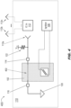
- FIG. 4 a fuse apparatus 400 is shown.
- the fuse apparatus 400 may include an energetic layer 106 and ignition circuit 108 that may be implemented and may function similarly to the anti-fuse apparatus 100, 200 of FIGS. 1 and 2 .
- the fuse apparatus 300 may be engaged to modify one or more input interfaces 112a-112-n to the IC 112 for identification strapping purposes.
- each of the interfaces 112a-112n may be associated with a default state wherein the conductive pads 114, 116 are electrically bridged by a closed circuit 402, such that each input may be readable or detectable as a logical-zero.
- the energetic layer 106 may be deposited over the closed circuit 402.
- the energetic layer 106 may be deposited via any additive manufacturing process elsewhere disclosed herein allowing for precise control over the surface area and/or thickness of the energetic layer.
- the ignition circuit 108 may be engaged (e.g., via a control circuit) to trigger a thermal reaction within the energetic layer 106.
- the thermal reaction may not generate sufficient heat to fracture or otherwise damage the substrate 110 (e.g., as opposed to a pyrotechnic or explosive reaction), but may render the material of the closed circuit 402 highly resistive, modifying the closed circuit to an open circuit for identification strapping purposes: e.g., any interface 112a-112n so modified may subsequently be readable or detectable as a logical-one rather than a logical-zero (e.g., the disconnected line pulled high by the resistor 122), such that the set of interfaces 112a-112n may collectively mechanically encode an n-bit binary identifier, e.g., a 48-bit unique MAC address.
- an n-bit binary identifier e.g., a 48-bit unique MAC address.
- the fuse apparatus 500 may be implemented and may function similarly to the fuse apparatus 400, except that the energetic layer 106 of the fuse apparatus 500 may be deposited over an electric bridge 502 connecting the input of a first IC 112 and the output of a second IC 504 (e.g., via the conductive pads 114, 116 respectively).
- the ignition circuit 108 may be engaged (e.g., via a control circuit, not shown) to trigger a thermal reaction within the energetic layer 106 and render the electric bridge 502 highly resistive, disabling the connection between the output IC 504 and the input IC 112 and likewise disabling any features associated with the input IC 112.
- the method 600 may be implemented by the anti-fuse apparatus 100, 200 and may include the following steps.
- a layer of low melting point dielectric material is deposited over a portion of a circuit board or other like substrate.
- the dielectric may be deposited between a pair of conductive pads set into the substrate, one conductive pad connected to an integrated circuit (IC) input and the two conductive pads not otherwise electrically connected.
- the second conductive pad is electrically coupled to a logical ground.
- the second conductive pad is electrically coupled to the output of another integrated circuit (e.g., such that the output of the second IC feeds into the input of the first IC).
- a layer of a low melting point conductive alloy is deposited over the dielectric layer when constructing the anti-fuse.
- a layer of energetic material is deposited over a portion of the conductive alloy layer.
- the energetic material may be deposited first, and the conductive alloy layer deposited over the energetic material.
- the energetic material may be deposited via aerosol jet printing or any like appropriate additive method providing precise control of footprint size and/or thickness.
- the energetic material is connected to an ignition circuit (e.g., which may be triggered or engaged by a control circuit, the ignition circuit and control circuit likewise set into the substrate).
- the ignition circuit triggers a thermal reaction in the energetic material.
- the heat generated melts and removes the dielectric layer, and similarly melts the conductive alloy layer such that the conductive alloy forms an electrical bridge connecting the two conductive pads.
- the conductive alloy layer may electrically bridge a conductive pad connecting two ICs (e.g., a second IC output to a first IC input) with another conductive pad electrically coupled to ground, grounding the output IC and disabling the interface between the two ICs.
- the conductive alloy layer may electrically bridge one or more ICs' inputs to one or more IC outputs, enabling I/O between the bridged ICs and enabling access to additional features associated with newly bridged ICs.
- embodiments of the methods disclosed herein may include one or more of the steps described herein. Further, such steps may be carried out in any desired order and two or more of the steps may be carried out simultaneously with one another. Two or more of the steps disclosed herein may be combined in a single step, and in some embodiments, one or more of the steps may be carried out as two or more sub-steps. Further, other steps or sub-steps may be carried in addition to, or as substitutes to one or more of the steps disclosed herein.
Landscapes
- Chemical & Material Sciences (AREA)
- Crystallography & Structural Chemistry (AREA)
- Organic Chemistry (AREA)
- Design And Manufacture Of Integrated Circuits (AREA)
Abstract
Description
- Leveraging commercial off the shelf (COTS) components often leads to use of third-party components and/or circuit boards that may not have a high degree of trust. For example, it may still be possible to bypass methods for enabling or disabling discrete circuit features based on COTS provided features. Methods for providing identification and feature strapping based on software stored variables (such as in Flash or E-Fuse) may still be reversible or overwritable.
- In a microelectronics system in package (SiP), many COTS components may be designed into a single package. In many instances, a single package will be designed with significant versatility to fit multiple use cases. However, with this versatility comes a need to enable or disable selected features, and/or provide methods of unique component identification, not based on COTS components within the package and therefore not vulnerable to trust issues or bypassability as noted above.
- In a first aspect, a microelectronic anti-fuse apparatus is disclosed. In embodiments, the anti-fuse apparatus includes a layer of dielectric material having a low melting point and deposited above a pair of conductive pads (e.g., which are below the dielectric layer but may or may not be under the dielectric layer) set into a substrate. The first pad is electrically coupled to an integrated circuit (IC) input, but the first and second pads are not otherwise initially electrically coupled to each other. A layer of conductive alloy having a low melting point is deposited over the dielectric layer. A layer of energetic material having a higher melting point is deposited over the conductive alloy layer and connected to an ignition circuit. When engaged by a control circuit, the ignition circuit triggers a thermal reaction in the energetic layer. The thermal reaction melts the dielectric and conductive alloy layers without otherwise damaging the underlying substrate, removing the dielectric layer and allowing the conductive alloy layer to electrically bridge the two conductive pads.
- In some embodiments, the second conductive pad (e.g., the conductive pad not coupled to the IC input) is electrically coupled to ground, and the thermal reaction grounds the IC input by electrically bridging the two conductive pads.
- In some embodiments, the second conductive pad (e.g., the conductive pad not coupled to the IC input) is electrically coupled to ground, the IC input is electrically interfaced with an output of another IC via the first conductive pad, and the thermal reaction disables the interface by bridging the two conductive pads and grounding the IC output.
- In some embodiments, the second conductive pad is also connected to a (second) IC (the IC input being associated with a first IC) and the thermal reaction enables input/output (I/O) between the first and second ICs, enabling access to features associated with the second IC by bridging the two conductive pads and therefore electrically bridging the first and second ICs.
- In some embodiments, the dielectric layer is deposited via aerosol jet printing, inkjet printing, or screenprinting.
- In some embodiments, the dielectric layer is deposited between the conductive pads, e.g., over conductive leads between the conductive pads but not over the conductive pads themselves.
- In some embodiments, the dielectric layer is deposited directly over the conductive pads.
- In a first aspect, a microelectronic anti-fuse apparatus is disclosed. In embodiments, the anti-fuse apparatus includes a layer of dielectric material having a low melting point and deposited above a pair of conductive pads (e.g., which are below the dielectric layer but may or may not be under the dielectric layer) set into a substrate. The first pad is electrically coupled to an integrated circuit (IC) input, but the first and second pads are not otherwise initially electrically coupled to each other. A layer of energetic material is deposited over the dielectric layer and connected to an ignition circuit. A layer of conductive alloy having a low melting point is deposited over the energetic layer. When engaged by a control circuit, the ignition circuit triggers a thermal reaction in the energetic layer. The thermal reaction melts the dielectric and conductive alloy layers without otherwise damaging the underlying substrate, removing the dielectric and energetic layers and allowing the conductive alloy layer to electrically bridge the two conductive pads.
- In some embodiments, the second conductive pad (e.g., the conductive pad not coupled to the IC input) is electrically coupled to ground, and the thermal reaction grounds the IC input by electrically bridging the two conductive pads.
- In some embodiments, the second conductive pad (e.g., the conductive pad not coupled to the IC input) is electrically coupled to ground, the IC input is electrically interfaced with an output of another IC via the first conductive pad, and the thermal reaction disables the interface by bridging the two conductive pads and grounding the IC output.
- In some embodiments, the second conductive pad is also connected to a (second) IC (the IC input being associated with a first IC) and the thermal reaction enables input/output (I/O) between the first and second ICs, enabling access to features associated with the second IC by bridging the two conductive pads and therefore electrically bridging the first and second ICs.
- In some embodiments, the dielectric layer is deposited via aerosol jet printing, inkjet printing, or screenprinting.
- In some embodiments, the dielectric layer is deposited between the conductive pads, e.g., over conductive leads between the conductive pads but not over the conductive pads themselves.
- In some embodiments, the dielectric layer is deposited directly over the conductive pads.
- In a still further aspect, a method for forming an anti-fuse apparatus on a substrate is also disclosed. In embodiments, the method includes depositing a layer of a dielectric material having a low melting point over a portion of a substrate, between (and, in some embodiments, directly over) a first conductive pad and a second conductive pad set into the substrate. The first conductive pad is electrically coupled to an integrated circuit (IC) input, but the first and second conductive pads are not otherwise electrically coupled to each other. The method includes depositing a layer of a low-melting-point conductive alloy over the dielectric layer. The method includes depositing an energetic material over some or all of the conductive alloy layer. The method includes connecting the energetic material to an ignition circuit capable of triggering a thermal reaction in the energetic material. The thermal reaction is capable of melting and removing the dielectric layer and melting the conductive alloy layer, allowing the conductive alloy layer to electrically bridge the conductive pads while avoiding generating sufficient heat or energy to otherwise damage the underlying substrate.
- This Summary is provided solely as an introduction to subject matter that is fully described in the Detailed Description and Drawings. The Summary should not be considered to describe essential features nor be used to determine the scope of the Claims. Moreover, it is to be understood that both the foregoing Summary and the following Detailed Description are example and explanatory only and are not necessarily restrictive of the subject matter claimed.
- The detailed description is described with reference to the accompanying figures. The use of the same reference numbers in different instances in the description and the figures may indicate similar or identical items. Various embodiments or examples ("examples") of the present disclosure are disclosed in the following detailed description and the accompanying drawings. The drawings are not necessarily to scale. In general, operations of disclosed processes may be performed in an arbitrary order, unless otherwise provided in the claims. In the drawings:
-
FIG. 1 is a diagrammatic illustration of an anti-fuse apparatus for identification strapping of an integrated circuit (IC) according to example embodiments of this disclosure; -
FIG. 2 is a diagrammatic illustration of an anti-fuse apparatus for disabling of additional IC features according to example embodiments of this disclosure; -
FIG. 3 is a diagrammatic illustration of an anti-fuse apparatus for enabling of additional IC features according to example embodiments of this disclosure; -
FIG. 4 is a diagrammatic illustration of a fuse apparatus for identification strapping of an IC according to example embodiments of this disclosure; -
FIG. 5 is a diagrammatic illustration of a fuse apparatus for disabling IC features according to example embodiments of this disclosure; - and
FIG. 6 is a flow diagram illustrating a method for forming an anti-fuse apparatus according to example embodiments of this disclosure. - Before explaining one or more embodiments of the disclosure in detail, it is to be understood that the embodiments are not limited in their application to the details of construction and the arrangement of the components or steps or methodologies set forth in the following description or illustrated in the drawings. In the following detailed description of embodiments, numerous specific details may be set forth in order to provide a more thorough understanding of the disclosure. However, it will be apparent to one of ordinary skill in the art having the benefit of the instant disclosure that the embodiments disclosed herein may be practiced without some of these specific details. In other instances, well-known features may not be described in detail to avoid unnecessarily complicating the instant disclosure.
- As used herein a letter following a reference numeral is intended to reference an embodiment of the feature or element that may be similar, but not necessarily identical, to a previously described element or feature bearing the same reference numeral (e.g., 1, 1a, 1b). Such shorthand notations are used for purposes of convenience only and should not be construed to limit the disclosure in any way unless expressly stated to the contrary.
- Further, unless expressly stated to the contrary, "or" refers to an inclusive or and not to an exclusive or. For example, a condition A or B is satisfied by any one of the following: A is true (or present) and B is false (or not present), A is false (or not present) and B is true (or present), and both A and B are true (or present).
- In addition, use of "a" or "an" may be employed to describe elements and components of embodiments disclosed herein. This is done merely for convenience and "a" and "an" are intended to include "one" or "at least one," and the singular also includes the plural unless it is obvious that it is meant otherwise.
- Finally, as used herein any reference to "one embodiment" or "some embodiments" means that a particular element, feature, structure, or characteristic described in connection with the embodiment is included in at least one embodiment disclosed herein. The appearances of the phrase "in some embodiments" in various places in the specification are not necessarily all referring to the same embodiment, and embodiments may include one or more of the features expressly described or inherently present herein, or any combination or sub-combination of two or more such features, along with any other features which may not necessarily be expressly described or inherently present in the instant disclosure.
- Broadly speaking, embodiments of the inventive concepts disclosed herein are directed to apparatus and methods for leveraging energetic materials on a microelectronic scale to create fuse and anti-fuse apparatus for the modification of identification (ID) strapping, fault flags, and/or circuit interconnectivity on a mechanical, irreversible basis. Accordingly, ID strapping and feature modification can be implemented on COTS components without the trust issues or vulnerabilities of said COTS components.
- Referring now to
FIG. 1 , a microelectronicanti-fuse apparatus 100 is shown. Theanti-fuse apparatus 100 may include adielectric layer 102,conductive alloy layer 104,energetic layer 106,ignition circuit 108, andsubstrate 110. - In embodiments, one or more components of the
anti-fuse apparatus 100 may be attached to asubstrate 110 via additive manufacturing methods. For example, thesubstrate 110 may include a system in package (SiP), bare die, circuit board, microelectronic device, backplane connector, Ethernet physical layer (PHY) device, electronic device, and/or mobile cellular/WiFi antenna. In embodiments, one or more integrated circuits 112 (IC) may likewise be attached to thesubstrate 110. - In embodiments, the
dielectric layer 102, e.g., one or more layers of dielectric material having a low melting point, may be similarly deposited over a portion of thesubstrate 110. For example, thedielectric layer 102 may include ultraviolet-cure epoxy resins (e.g., MasterBond UV15, Loctite EA3335), polyimides, or any other appropriate dielectric deposited over high melting pointconductive metal pads 114, 116 (e.g., or electric leads 118 electrically coupled to said conductive pads) which in turn may be positioned over a portion of thesubstrate 110. With respect to thedielectric layer 102 and theconductive alloy layer 104, the incorporation of relatively lower-melting-point components requires less thermal energy to melt, and therefore minimizes the risk of damage to, or destruction of, theunderlying substrate 110 as a result of the thermal reaction. - In embodiments, the
dielectric layer 102 may be deposited over thesubstrate 110 between twoconductive pads conductive pad 114 may be electrically coupled to an input of theIC 112 and/or a power supply (e.g., common collector voltage V cc ). Further, the otherconductive pad 116 may be electrically coupled to aground 120. In embodiments, thedielectric layer 102 may be deposited over the substrate 110 (e.g., over a portion thereof) such that electric leads 118 between theconductive pads conductive alloy layer 104 by thedielectric layer 102. In some embodiments, theconductive pads dielectric layer 102, theconductive alloy 104, and theenergetic layer 106, e.g., the said layers are deposited directly over the conductive pads (e.g., in which case the electric leads 118 are not needed). - In embodiments, the
conductive alloy layer 104 may comprise a quantity of metal alloy having a low melting point (e.g., lower than that of the energetic layer 106). For example, the conductive alloy layer may likewise be deposited over the electric leads 118 but insulated therefrom by thedielectric layer 102. In embodiments, theconductive alloy layer 104 may include, but is not limited to, tin (Sn) or any of the following alloys: tin/lead (SnPb), bismuth/tin (BiSn), bismuth/tin/silver (BiSnAg), tin/indium/silver (SnInAg). Further, theconductive alloy layer 104 may be deposited via one or more methods including, but not limited to, alloy paste screening, preshaping (e.g., into a resistor shape) and pick-and-place deposition, placement by hand, and/or any other appropriate method capable of depositing theconductive alloy layer 104 without disturbing or damaging theunderlying dielectric layer 102. - In embodiments, the
energetic layer 106 may be deposited over theconductive alloy layer 104 according to any appropriate deposition methods (e.g., controlled direct-write (e.g., inkjet printing, liquid deposition, extrusion), aerosol jet printing, fused-filament fabrication) capable of providing precise control for the feature size of the energetic layer. Further, theenergetic layer 106 may include one or more nanothermite, pyrotechnic, or explosive compounds as disclosed inU.S. Patent App. 17/120,574 and incorporated by reference herein in their entirety, but not sufficiently thickly or densely applied as to be capable of causing a pyrotechnic or explosive reaction damaging to (or destructive to) thesubstrate 110. In some embodiments, theconductive alloy layer 104 may be deposited above theenergetic layer 106. For example, in some cases theenergetic layer 106 may have a lower melting point, such that the thermal reaction triggered by the ignition circuit melts and removes the energetic layer as well as the dielectric layer, leaving the meltedconductive alloy layer 104 to bridge the conductive pads. - In embodiments, the
energetic layer 106 may be connected to anignition circuit 108, which likewise may be attached to thesubstrate 110. For example, the ignition circuit 108 (e.g., on engagement or initiation by a control circuit) may trigger a thermal reaction with respect to theenergetic layer 106, providing sufficient heat as to melt both thedielectric layer 102 and theconductive alloy layer 104, removing the dielectric layer and allowing the melted conductive alloy layer to complete an electrical bridge between the underlyingconductive pads 114, 116 (e.g., thus connecting theIC 112 and the ground 120). However, the thermal reaction triggered by theignition circuit 108 may be limited to a small footprint including thedielectric layer 102 andconductive alloy layer 104, so as not to fracture or otherwise damage thesubstrate 110. - In embodiments, the
IC 112 may be identification (ID) strapped in order to uniquely identify the IC among a set of many such otherwise identical ICs. For example, theIC 112 may be associated with an Ethernet device having a media access control (MAC) address (e.g., a 48-bit, 12-digit hexadecimal) or like unique identifier. In embodiments, theIC 112 may be "marked" with the corresponding MAC address in a mechanical and permanent way that does not leave the substrate or IC open to tampering or to exploitation of vulnerabilities associated with COTS components, and that does not otherwise damage the substrate. For example, theIC 112 may have a series of discretehardwired input interfaces 112a-112n, e.g., 48 interfaces, each input interface capable of a shorted state or an open (e.g., grounded) state readable by a digital circuit interface as either a logical one or a logical zero respectively. In embodiments, each of theinterfaces 112a-112n to theIC 112 may be associated with a default state wherein theconductive pads resistor 122 pulls the line high, such that the state of the interface may be interpreted as a logical-one. In embodiments, theignition circuits 108 for selectedinterfaces 112a-112n may be engaged by a control circuit (not shown) to selectively trigger the thermal reaction in their respectiveenergetic layers 106, removing their respectivedielectric layers 102 and melting their respective conductive alloy layers 104 to electrically bridge theconductive pads ground 120. For example, each of the resulting grounded interfaces distributed within 112a-112n may be interpreted as a logical-zero, while each of the untriggered interfaces distributed within 112a-112n may be interpreted as a logical-one, and the full set of interfaces may represent the 48-bit MAC address. - Referring now to
FIG. 2 , theanti-fuse apparatus 200 may be implemented and may function similarly to theanti-fuse apparatus 100 ofFIG. 1 , except that theanti-fuse apparatus 200 may be engaged to disable additional features with respect to thesubstrate 110 and/orcomponent ICs - In embodiments, the
substrate 110 may include anIC output 202 electrically coupled to an input of theIC 112 via theconductive pad 114. For example, theignition circuit 108 may be engaged (e.g., via control circuit, not shown) to trigger a thermal reaction with respect to theenergetic layer 106, melt and remove thedielectric layer 102, and melt theconductive alloy layer 104 so as to disable the electrical coupling between theICs ground 120. Further, the meltedconductive alloy layer 104 may form an electrical bridge between theconductive pads resistor 204 on the output of theIC 202, preventing damage to the IC due to the grounding. - Referring now to
FIG. 3 theanti-fuse apparatus 300 may be implemented and may function similarly to theanti-fuse apparatus 100 ofFIG. 1 , except that theanti-fuse apparatus 300 may be engaged to enable additional features with respect to thesubstrate 110 and/orcomponent ICs 112, 302. - In embodiments, and as described above with respect to the anti-fuse apparatus of
FIG. 1 , theignition circuit 108 may be engaged (e.g., via control panel, not shown) to trigger a thermal reaction within theenergetic layer 106, removing thedielectric layer 102, melting theconductive alloy layer 104, and bridging theconductive pads conductive pads IC 112 and the IC 302, enabling access to features associated with the IC 302. It may be noted that with respect to the anti-fuse apparatus 300 (and as noted above with respect to the anti-fuse apparatus ofFIG. 1 ), theconductive pads conductive alloy layer 104. - Referring now to
FIG. 4 , afuse apparatus 400 is shown. - Commonly owned
U.S. Patent Application 17/120,574 , which is incorporated herein by reference in its entirety, discloses an anti-tamper architecture based on the addition of energetic materials to a COTS device. However, said anti-temper architecture involves the use of pyrotechnic and/or explosive compounds to permanently fracture or destroy the device via exothermic reaction. - In embodiments, the
fuse apparatus 400 may include anenergetic layer 106 andignition circuit 108 that may be implemented and may function similarly to theanti-fuse apparatus FIGS. 1 and2 . In particular, similarly to theanti-fuse apparatus 100, thefuse apparatus 300 may be engaged to modify one ormore input interfaces 112a-112-n to theIC 112 for identification strapping purposes. For example, each of theinterfaces 112a-112n may be associated with a default state wherein theconductive pads closed circuit 402, such that each input may be readable or detectable as a logical-zero. - In embodiments, with respect to the
fuse apparatus 400, theenergetic layer 106 may be deposited over theclosed circuit 402. For example, theenergetic layer 106 may be deposited via any additive manufacturing process elsewhere disclosed herein allowing for precise control over the surface area and/or thickness of the energetic layer. In embodiments, theignition circuit 108 may be engaged (e.g., via a control circuit) to trigger a thermal reaction within theenergetic layer 106. For example, the thermal reaction may not generate sufficient heat to fracture or otherwise damage the substrate 110 (e.g., as opposed to a pyrotechnic or explosive reaction), but may render the material of theclosed circuit 402 highly resistive, modifying the closed circuit to an open circuit for identification strapping purposes: e.g., anyinterface 112a-112n so modified may subsequently be readable or detectable as a logical-one rather than a logical-zero (e.g., the disconnected line pulled high by the resistor 122), such that the set ofinterfaces 112a-112n may collectively mechanically encode an n-bit binary identifier, e.g., a 48-bit unique MAC address. - Referring now to
FIG. 5 , thefuse apparatus 500 may be implemented and may function similarly to thefuse apparatus 400, except that theenergetic layer 106 of thefuse apparatus 500 may be deposited over anelectric bridge 502 connecting the input of afirst IC 112 and the output of a second IC 504 (e.g., via theconductive pads ignition circuit 108 may be engaged (e.g., via a control circuit, not shown) to trigger a thermal reaction within theenergetic layer 106 and render theelectric bridge 502 highly resistive, disabling the connection between theoutput IC 504 and theinput IC 112 and likewise disabling any features associated with theinput IC 112. - Referring now to
FIG. 6 , themethod 600 may be implemented by theanti-fuse apparatus - At a
step 602, a layer of low melting point dielectric material is deposited over a portion of a circuit board or other like substrate. For example, the dielectric may be deposited between a pair of conductive pads set into the substrate, one conductive pad connected to an integrated circuit (IC) input and the two conductive pads not otherwise electrically connected. In some embodiments, the second conductive pad is electrically coupled to a logical ground. In other embodiments, the second conductive pad is electrically coupled to the output of another integrated circuit (e.g., such that the output of the second IC feeds into the input of the first IC). - At a
step 604, a layer of a low melting point conductive alloy is deposited over the dielectric layer when constructing the anti-fuse. - At a
step 606, a layer of energetic material is deposited over a portion of the conductive alloy layer. In some embodiments, the energetic material may be deposited first, and the conductive alloy layer deposited over the energetic material. For example, the energetic material may be deposited via aerosol jet printing or any like appropriate additive method providing precise control of footprint size and/or thickness. - At a
step 608, the energetic material is connected to an ignition circuit (e.g., which may be triggered or engaged by a control circuit, the ignition circuit and control circuit likewise set into the substrate). For example, when triggered by the control circuit, the ignition circuit triggers a thermal reaction in the energetic material. The heat generated melts and removes the dielectric layer, and similarly melts the conductive alloy layer such that the conductive alloy forms an electrical bridge connecting the two conductive pads. In some embodiments, e.g., the conductive alloy layer may electrically bridge a conductive pad connecting two ICs (e.g., a second IC output to a first IC input) with another conductive pad electrically coupled to ground, grounding the output IC and disabling the interface between the two ICs. In some embodiments, the conductive alloy layer may electrically bridge one or more ICs' inputs to one or more IC outputs, enabling I/O between the bridged ICs and enabling access to additional features associated with newly bridged ICs. - It is to be understood that embodiments of the methods disclosed herein may include one or more of the steps described herein. Further, such steps may be carried out in any desired order and two or more of the steps may be carried out simultaneously with one another. Two or more of the steps disclosed herein may be combined in a single step, and in some embodiments, one or more of the steps may be carried out as two or more sub-steps. Further, other steps or sub-steps may be carried in addition to, or as substitutes to one or more of the steps disclosed herein.
- Although inventive concepts have been described with reference to the embodiments illustrated in the attached drawing figures, equivalents may be employed and substitutions made herein without departing from the scope of the claims. Components illustrated and described herein are merely examples of a system/device and components that may be used to implement embodiments of the inventive concepts and may be replaced with other devices and components without departing from the scope of the claims. Furthermore, any dimensions, degrees, and/or numerical ranges provided herein are to be understood as non-limiting examples unless otherwise specified in the claims.
Claims (15)
- An apparatus, comprising:at least one layer of a dielectric material (102) deposited above a first and a second conductive pad (114, 116) set into a substrate (110), the first conductive pad electrically coupled to an integrated circuit, IC, input (112), the first and second conductive pads (114, 116) not otherwise electrically coupled to each other;at least one layer of a conductive alloy (104) deposited above the dielectric layer (102);
andat least one layer of an energetic material (106) deposited above the conductive alloy layer (104), the energetic material coupled to an ignition circuit (108);whereinthe ignition circuit (108) is configured to trigger a thermal reaction in the energetic material (106), the thermal reaction capable of:1) removing the at least one dielectric layer (102);2) melting the at least one conductive alloy layer (104);
and3) electrically bridging the first and second conductive pads (114, 116) via the conductive alloy (104). - The apparatus of Claim 1, wherein:the second conductive pad (116) is electrically coupled to a ground (120);
andthe thermal reaction is configured to ground the IC input (112) by electrically bridging the first and second conductive pads (114, 116). - The apparatus of Claim 1, wherein:the second conductive pad (116) is electrically coupled to a ground (120);the IC input (112) is electrically coupled to at least one second IC output (202) via the first conductive pad (114);
andthe thermal reaction is capable of 1) disabling the electrical coupling of the IC input (112) and the IC output (202) by grounding the at least one second IC output. - The apparatus of Claim 1, wherein:the IC input (112) is associated with a first IC;the second conductive pad (116) is electrically coupled to a second IC;
andthe electrical bridge between the first and second ICs is capable of enabling input/output (I/O) between the first and second ICs. - The apparatus of any preceding Claim, wherein the at least one dielectric layer (102) is deposited via at least one of aerosol jet printing, inkjet printing, or screen printing.
- The apparatus of any preceding Claim, wherein the at least one dielectric layer (102) is deposited between the first and the second conductive pads (114, 116).
- The apparatus of any of Claims 1-5, wherein the at least one dielectric layer (102) is deposited over the first and the second conductive pads (114, 116).
- An apparatus, comprising:a first conductive pad (114) and a second conductive pad (116) set into a substrate (110), the first conductive pad (114) electrically coupled to an integrated circuit, IC, input (112), the first and second conductive pads (114, 116) not otherwise electrically coupled to each other;at least one layer of a dielectric material (102) deposited above the first and second conductive pads (114, 116);at least one layer of an energetic material (106) deposited above the dielectric layer, the energetic material coupled to an ignition circuit (108);
andat least one layer of a conductive alloy (104) deposited above the energetic layer;whereinthe ignition circuit (108) is configured to trigger a thermal reaction in the energetic material (106), the thermal reaction capable of:1) removing the at least one dielectric layer (102) and the at least one energetic layer (106);2) melting the at least one conductive alloy layer (104);
and3) electrically bridging the first and second conductive pads (114, 116) via the conductive alloy (104). - The apparatus of Claim 8, wherein:the second conductive pad (116) is electrically coupled to a ground (120);
andthe thermal reaction is configured to ground the IC input (112) by electrically bridging the first and second conductive pads (114, 116). - The apparatus of Claim 8, wherein:the second conductive pad (116) is electrically coupled to a ground (120);the IC input (112) is electrically coupled to at least one second IC output (202) via the first conductive pad (114);
andthe thermal reaction is capable of 1) disabling the electrical coupling of the IC input (112) and the IC output (202) by grounding the at least one second IC output. - The apparatus of Claim 8, wherein:the IC input (112) is associated with a first IC;the second conductive pad (114) is electrically coupled to a second IC;
andthe electrical bridge between the first and second ICs is capable of enabling input/output (I/O) between the first and second ICs. - The apparatus of any of Claims 8-11, wherein the at least one dielectric layer (102) is deposited via at least one of aerosol jet printing, inkjet printing, or screen printing.
- The apparatus of any of Claims 8-12, wherein the at least one dielectric layer (102) is deposited between the first and the second conductive pads (114, 116).
- The apparatus of any of Claims 8-12, wherein the at least one dielectric layer (102) is deposited over the first and the second conductive pads (114, 116).
- A method for forming an anti-fuse on an apparatus, the method comprising:depositing a layer of a dielectric material over a portion of a substrate, the portion including a first conductive pad and a second conductive pad set thereinto, the first conductive pad electrically coupled to an integrated circuit (IC) input, the first and second conductive pads not otherwise electrically coupled to each other;depositing a layer of a conductive alloy over the dielectric layer;depositing, via an additive manufacturing method, at least one layer of an energetic material over a portion of the conductive alloy layer;connecting the at least one layer of the energetic material to an ignition circuit, the ignition circuit configured to trigger a thermal reaction in the at least one energetic layer, the thermal reaction capable of:1) removing the at least one dielectric layer;2) melting the at least one conductive alloy layer;
and3) electrically bridging the first and second conductive pads via the conductive alloy.
Applications Claiming Priority (1)
| Application Number | Priority Date | Filing Date | Title |
|---|---|---|---|
| US18/213,612 US20240429160A1 (en) | 2023-06-23 | 2023-06-23 | Microelectronic mechanical fuse and anti-fuse apparatus and method |
Publications (3)
| Publication Number | Publication Date |
|---|---|
| EP4481810A2 true EP4481810A2 (en) | 2024-12-25 |
| EP4481810A3 EP4481810A3 (en) | 2025-01-08 |
| EP4481810B1 EP4481810B1 (en) | 2025-10-22 |
Family
ID=91580970
Family Applications (1)
| Application Number | Title | Priority Date | Filing Date |
|---|---|---|---|
| EP24182396.2A Active EP4481810B1 (en) | 2023-06-23 | 2024-06-14 | Microelectronic mechanical fuse and anti-fuse apparatus and method |
Country Status (2)
| Country | Link |
|---|---|
| US (1) | US20240429160A1 (en) |
| EP (1) | EP4481810B1 (en) |
Family Cites Families (10)
| Publication number | Priority date | Publication date | Assignee | Title |
|---|---|---|---|---|
| US3725671A (en) * | 1970-11-02 | 1973-04-03 | Us Navy | Pyrotechnic eradication of microcircuits |
| US9905265B2 (en) * | 2007-12-03 | 2018-02-27 | Jonathan Mohler | Destructive system having a functional layer and an adjacent reactive layer and an associated method |
| US8861728B2 (en) * | 2012-10-17 | 2014-10-14 | International Business Machines Corporation | Integrated circuit tamper detection and response |
| JP6420053B2 (en) * | 2013-03-28 | 2018-11-07 | デクセリアルズ株式会社 | Fuse element and fuse element |
| DE102016208419B4 (en) * | 2016-05-17 | 2025-12-18 | Fraunhofer-Gesellschaft zur Förderung der angewandten Forschung e.V. | Electrical bridging device for bridging an electrical energy source or energy consumer |
| US11332254B2 (en) * | 2019-12-16 | 2022-05-17 | Goodrich Corporation | Pyrotechnic energy conversion system for ejection assembly |
| US12354817B2 (en) * | 2020-02-19 | 2025-07-08 | Siemens Energy Global GmbH & Co. KG | Short-circuit switching device including at least one pyrotechnic ignition device |
| CN111739850A (en) * | 2020-07-09 | 2020-10-02 | 中国人民解放军92228部队 | A self-destructing chip embedded with an energy-containing film and a preparation method thereof |
| US11877389B2 (en) * | 2020-12-14 | 2024-01-16 | Rockwell Collins, Inc. | Additively manufactured energetic material anti-tamper feature and implementation |
| TWI866440B (en) * | 2023-09-04 | 2024-12-11 | 聚鼎科技股份有限公司 | Protection device |
-
2023
- 2023-06-23 US US18/213,612 patent/US20240429160A1/en active Pending
-
2024
- 2024-06-14 EP EP24182396.2A patent/EP4481810B1/en active Active
Also Published As
| Publication number | Publication date |
|---|---|
| US20240429160A1 (en) | 2024-12-26 |
| EP4481810A3 (en) | 2025-01-08 |
| EP4481810B1 (en) | 2025-10-22 |
Similar Documents
| Publication | Publication Date | Title |
|---|---|---|
| US7703201B2 (en) | Method of embedding tamper proof layers and discrete components into printed circuit board stack-up | |
| CN104934954B (en) | Fuse-resistor | |
| JP2009544838A5 (en) | ||
| US10566164B2 (en) | Temperature-triggered fuse device and method of production thereof | |
| CN104882342B (en) | Composite protection device | |
| US20110132645A1 (en) | Granular varistor and applications for use thereof | |
| JPH0779196B2 (en) | Wiring change method | |
| EP4481810B1 (en) | Microelectronic mechanical fuse and anti-fuse apparatus and method | |
| KR20150083810A (en) | Ceramic chip fuse with offset fuse element | |
| JP6388427B2 (en) | Wafer scale manufacturing method for surface mount electronic module | |
| KR20120064678A (en) | Rapid activation fusible link | |
| US6364731B1 (en) | Circuit device manufacturing equipment | |
| JP4823201B2 (en) | Circuit board | |
| US6380059B1 (en) | Method of breaking electrically conductive traces on substrate into open-circuited state | |
| US7961450B2 (en) | Antistatic apparatus | |
| KR100331129B1 (en) | Fault-current fuse resistors and methods | |
| KR102956628B1 (en) | Circuit Board | |
| KR101026258B1 (en) | Micro Fuses for Printed Circuit Boards | |
| CN213342817U (en) | A circuit board and electronic equipment | |
| GB2345187A (en) | Metal oxide varistors | |
| US20240274595A1 (en) | Integrated circuit with protective element | |
| CN118486683A (en) | Integrated circuit with protective element | |
| CN121532848A (en) | Circuit with resistive fuse | |
| CN114121900A (en) | ESD device processing method with overvoltage and overcurrent protection | |
| CN119486263A (en) | Display module, method for manufacturing display module, and display device |
Legal Events
| Date | Code | Title | Description |
|---|---|---|---|
| PUAI | Public reference made under article 153(3) epc to a published international application that has entered the european phase |
Free format text: ORIGINAL CODE: 0009012 |
|
| STAA | Information on the status of an ep patent application or granted ep patent |
Free format text: STATUS: THE APPLICATION HAS BEEN PUBLISHED |
|
| PUAL | Search report despatched |
Free format text: ORIGINAL CODE: 0009013 |
|
| AK | Designated contracting states |
Kind code of ref document: A2 Designated state(s): AL AT BE BG CH CY CZ DE DK EE ES FI FR GB GR HR HU IE IS IT LI LT LU LV MC ME MK MT NL NO PL PT RO RS SE SI SK SM TR |
|
| AK | Designated contracting states |
Kind code of ref document: A3 Designated state(s): AL AT BE BG CH CY CZ DE DK EE ES FI FR GB GR HR HU IE IS IT LI LT LU LV MC ME MK MT NL NO PL PT RO RS SE SI SK SM TR |
|
| RIC1 | Information provided on ipc code assigned before grant |
Ipc: H01L 23/525 20060101AFI20241202BHEP |
|
| STAA | Information on the status of an ep patent application or granted ep patent |
Free format text: STATUS: REQUEST FOR EXAMINATION WAS MADE |
|
| 17P | Request for examination filed |
Effective date: 20250218 |
|
| GRAP | Despatch of communication of intention to grant a patent |
Free format text: ORIGINAL CODE: EPIDOSNIGR1 |
|
| STAA | Information on the status of an ep patent application or granted ep patent |
Free format text: STATUS: GRANT OF PATENT IS INTENDED |
|
| RIC1 | Information provided on ipc code assigned before grant |
Ipc: C06B 45/12 20060101ALI20250515BHEP Ipc: H05K 1/02 20060101ALI20250515BHEP Ipc: H01L 23/525 20060101AFI20250515BHEP |
|
| INTG | Intention to grant announced |
Effective date: 20250603 |
|
| GRAS | Grant fee paid |
Free format text: ORIGINAL CODE: EPIDOSNIGR3 |
|
| GRAA | (expected) grant |
Free format text: ORIGINAL CODE: 0009210 |
|
| STAA | Information on the status of an ep patent application or granted ep patent |
Free format text: STATUS: THE PATENT HAS BEEN GRANTED |
|
| AK | Designated contracting states |
Kind code of ref document: B1 Designated state(s): AL AT BE BG CH CY CZ DE DK EE ES FI FR GB GR HR HU IE IS IT LI LT LU LV MC ME MK MT NL NO PL PT RO RS SE SI SK SM TR |
|
| REG | Reference to a national code |
Ref country code: CH Ref legal event code: F10 Free format text: ST27 STATUS EVENT CODE: U-0-0-F10-F00 (AS PROVIDED BY THE NATIONAL OFFICE) Effective date: 20251022 Ref country code: GB Ref legal event code: FG4D |
|
| REG | Reference to a national code |
Ref country code: DE Ref legal event code: R096 Ref document number: 602024001005 Country of ref document: DE |
|
| REG | Reference to a national code |
Ref country code: IE Ref legal event code: FG4D |
|
| REG | Reference to a national code |
Ref country code: DE Ref legal event code: R079 Ref document number: 602024001005 Country of ref document: DE Free format text: PREVIOUS MAIN CLASS: H01L0023525000 Ipc: H10W0020490000 |
|
| REG | Reference to a national code |
Ref country code: NL Ref legal event code: MP Effective date: 20251022 |
|
| PG25 | Lapsed in a contracting state [announced via postgrant information from national office to epo] |
Ref country code: NL Free format text: LAPSE BECAUSE OF FAILURE TO SUBMIT A TRANSLATION OF THE DESCRIPTION OR TO PAY THE FEE WITHIN THE PRESCRIBED TIME-LIMIT Effective date: 20251022 |
|
| PG25 | Lapsed in a contracting state [announced via postgrant information from national office to epo] |
Ref country code: ES Free format text: LAPSE BECAUSE OF FAILURE TO SUBMIT A TRANSLATION OF THE DESCRIPTION OR TO PAY THE FEE WITHIN THE PRESCRIBED TIME-LIMIT Effective date: 20251022 |
|
| REG | Reference to a national code |
Ref country code: LT Ref legal event code: MG9D |
|
| PG25 | Lapsed in a contracting state [announced via postgrant information from national office to epo] |
Ref country code: NO Free format text: LAPSE BECAUSE OF FAILURE TO SUBMIT A TRANSLATION OF THE DESCRIPTION OR TO PAY THE FEE WITHIN THE PRESCRIBED TIME-LIMIT Effective date: 20260122 |
|
| PG25 | Lapsed in a contracting state [announced via postgrant information from national office to epo] |
Ref country code: HR Free format text: LAPSE BECAUSE OF FAILURE TO SUBMIT A TRANSLATION OF THE DESCRIPTION OR TO PAY THE FEE WITHIN THE PRESCRIBED TIME-LIMIT Effective date: 20251022 Ref country code: AT Free format text: LAPSE BECAUSE OF FAILURE TO SUBMIT A TRANSLATION OF THE DESCRIPTION OR TO PAY THE FEE WITHIN THE PRESCRIBED TIME-LIMIT Effective date: 20251022 Ref country code: FI Free format text: LAPSE BECAUSE OF FAILURE TO SUBMIT A TRANSLATION OF THE DESCRIPTION OR TO PAY THE FEE WITHIN THE PRESCRIBED TIME-LIMIT Effective date: 20251022 |
|
| REG | Reference to a national code |
Ref country code: AT Ref legal event code: MK05 Ref document number: 1850001 Country of ref document: AT Kind code of ref document: T Effective date: 20251022 |
|
| PG25 | Lapsed in a contracting state [announced via postgrant information from national office to epo] |
Ref country code: RS Free format text: LAPSE BECAUSE OF FAILURE TO SUBMIT A TRANSLATION OF THE DESCRIPTION OR TO PAY THE FEE WITHIN THE PRESCRIBED TIME-LIMIT Effective date: 20260122 |
|
| PG25 | Lapsed in a contracting state [announced via postgrant information from national office to epo] |
Ref country code: IS Free format text: LAPSE BECAUSE OF FAILURE TO SUBMIT A TRANSLATION OF THE DESCRIPTION OR TO PAY THE FEE WITHIN THE PRESCRIBED TIME-LIMIT Effective date: 20260222 |
|
| PG25 | Lapsed in a contracting state [announced via postgrant information from national office to epo] |
Ref country code: PT Free format text: LAPSE BECAUSE OF FAILURE TO SUBMIT A TRANSLATION OF THE DESCRIPTION OR TO PAY THE FEE WITHIN THE PRESCRIBED TIME-LIMIT Effective date: 20260223 |
|
| PG25 | Lapsed in a contracting state [announced via postgrant information from national office to epo] |
Ref country code: PL Free format text: LAPSE BECAUSE OF FAILURE TO SUBMIT A TRANSLATION OF THE DESCRIPTION OR TO PAY THE FEE WITHIN THE PRESCRIBED TIME-LIMIT Effective date: 20251022 |
|
| PG25 | Lapsed in a contracting state [announced via postgrant information from national office to epo] |
Ref country code: LV Free format text: LAPSE BECAUSE OF FAILURE TO SUBMIT A TRANSLATION OF THE DESCRIPTION OR TO PAY THE FEE WITHIN THE PRESCRIBED TIME-LIMIT Effective date: 20251022 |
|
| PG25 | Lapsed in a contracting state [announced via postgrant information from national office to epo] |
Ref country code: BG Free format text: LAPSE BECAUSE OF FAILURE TO SUBMIT A TRANSLATION OF THE DESCRIPTION OR TO PAY THE FEE WITHIN THE PRESCRIBED TIME-LIMIT Effective date: 20251022 |