EP4481796A1 - Method for growing diamond on silicon substrate and method for selectively growing diamond on silicon substrate - Google Patents
Method for growing diamond on silicon substrate and method for selectively growing diamond on silicon substrate Download PDFInfo
- Publication number
- EP4481796A1 EP4481796A1 EP23756127.9A EP23756127A EP4481796A1 EP 4481796 A1 EP4481796 A1 EP 4481796A1 EP 23756127 A EP23756127 A EP 23756127A EP 4481796 A1 EP4481796 A1 EP 4481796A1
- Authority
- EP
- European Patent Office
- Prior art keywords
- silicon substrate
- diamond
- pretreatment
- growing diamond
- growth
- Prior art date
- Legal status (The legal status is an assumption and is not a legal conclusion. Google has not performed a legal analysis and makes no representation as to the accuracy of the status listed.)
- Pending
Links
Images


Classifications
-
- C—CHEMISTRY; METALLURGY
- C01—INORGANIC CHEMISTRY
- C01B—NON-METALLIC ELEMENTS; COMPOUNDS THEREOF; METALLOIDS OR COMPOUNDS THEREOF NOT COVERED BY SUBCLASS C01C
- C01B32/00—Carbon; Compounds thereof
- C01B32/25—Diamond
-
- C—CHEMISTRY; METALLURGY
- C23—COATING METALLIC MATERIAL; COATING MATERIAL WITH METALLIC MATERIAL; CHEMICAL SURFACE TREATMENT; DIFFUSION TREATMENT OF METALLIC MATERIAL; COATING BY VACUUM EVAPORATION, BY SPUTTERING, BY ION IMPLANTATION OR BY CHEMICAL VAPOUR DEPOSITION, IN GENERAL; INHIBITING CORROSION OF METALLIC MATERIAL OR INCRUSTATION IN GENERAL
- C23C—COATING METALLIC MATERIAL; COATING MATERIAL WITH METALLIC MATERIAL; SURFACE TREATMENT OF METALLIC MATERIAL BY DIFFUSION INTO THE SURFACE, BY CHEMICAL CONVERSION OR SUBSTITUTION; COATING BY VACUUM EVAPORATION, BY SPUTTERING, BY ION IMPLANTATION OR BY CHEMICAL VAPOUR DEPOSITION, IN GENERAL
- C23C16/00—Chemical coating by decomposition of gaseous compounds, without leaving reaction products of surface material in the coating, i.e. chemical vapour deposition [CVD] processes
- C23C16/02—Pretreatment of the material to be coated
-
- C—CHEMISTRY; METALLURGY
- C23—COATING METALLIC MATERIAL; COATING MATERIAL WITH METALLIC MATERIAL; CHEMICAL SURFACE TREATMENT; DIFFUSION TREATMENT OF METALLIC MATERIAL; COATING BY VACUUM EVAPORATION, BY SPUTTERING, BY ION IMPLANTATION OR BY CHEMICAL VAPOUR DEPOSITION, IN GENERAL; INHIBITING CORROSION OF METALLIC MATERIAL OR INCRUSTATION IN GENERAL
- C23C—COATING METALLIC MATERIAL; COATING MATERIAL WITH METALLIC MATERIAL; SURFACE TREATMENT OF METALLIC MATERIAL BY DIFFUSION INTO THE SURFACE, BY CHEMICAL CONVERSION OR SUBSTITUTION; COATING BY VACUUM EVAPORATION, BY SPUTTERING, BY ION IMPLANTATION OR BY CHEMICAL VAPOUR DEPOSITION, IN GENERAL
- C23C16/00—Chemical coating by decomposition of gaseous compounds, without leaving reaction products of surface material in the coating, i.e. chemical vapour deposition [CVD] processes
- C23C16/02—Pretreatment of the material to be coated
- C23C16/0254—Physical treatment to alter the texture of the surface, e.g. scratching or polishing
-
- C—CHEMISTRY; METALLURGY
- C23—COATING METALLIC MATERIAL; COATING MATERIAL WITH METALLIC MATERIAL; CHEMICAL SURFACE TREATMENT; DIFFUSION TREATMENT OF METALLIC MATERIAL; COATING BY VACUUM EVAPORATION, BY SPUTTERING, BY ION IMPLANTATION OR BY CHEMICAL VAPOUR DEPOSITION, IN GENERAL; INHIBITING CORROSION OF METALLIC MATERIAL OR INCRUSTATION IN GENERAL
- C23C—COATING METALLIC MATERIAL; COATING MATERIAL WITH METALLIC MATERIAL; SURFACE TREATMENT OF METALLIC MATERIAL BY DIFFUSION INTO THE SURFACE, BY CHEMICAL CONVERSION OR SUBSTITUTION; COATING BY VACUUM EVAPORATION, BY SPUTTERING, BY ION IMPLANTATION OR BY CHEMICAL VAPOUR DEPOSITION, IN GENERAL
- C23C16/00—Chemical coating by decomposition of gaseous compounds, without leaving reaction products of surface material in the coating, i.e. chemical vapour deposition [CVD] processes
- C23C16/04—Coating on selected surface areas, e.g. using masks
-
- C—CHEMISTRY; METALLURGY
- C23—COATING METALLIC MATERIAL; COATING MATERIAL WITH METALLIC MATERIAL; CHEMICAL SURFACE TREATMENT; DIFFUSION TREATMENT OF METALLIC MATERIAL; COATING BY VACUUM EVAPORATION, BY SPUTTERING, BY ION IMPLANTATION OR BY CHEMICAL VAPOUR DEPOSITION, IN GENERAL; INHIBITING CORROSION OF METALLIC MATERIAL OR INCRUSTATION IN GENERAL
- C23C—COATING METALLIC MATERIAL; COATING MATERIAL WITH METALLIC MATERIAL; SURFACE TREATMENT OF METALLIC MATERIAL BY DIFFUSION INTO THE SURFACE, BY CHEMICAL CONVERSION OR SUBSTITUTION; COATING BY VACUUM EVAPORATION, BY SPUTTERING, BY ION IMPLANTATION OR BY CHEMICAL VAPOUR DEPOSITION, IN GENERAL
- C23C16/00—Chemical coating by decomposition of gaseous compounds, without leaving reaction products of surface material in the coating, i.e. chemical vapour deposition [CVD] processes
- C23C16/22—Chemical coating by decomposition of gaseous compounds, without leaving reaction products of surface material in the coating, i.e. chemical vapour deposition [CVD] processes characterised by the deposition of inorganic material, other than metallic material
- C23C16/26—Deposition of carbon only
- C23C16/27—Diamond only
-
- C—CHEMISTRY; METALLURGY
- C23—COATING METALLIC MATERIAL; COATING MATERIAL WITH METALLIC MATERIAL; CHEMICAL SURFACE TREATMENT; DIFFUSION TREATMENT OF METALLIC MATERIAL; COATING BY VACUUM EVAPORATION, BY SPUTTERING, BY ION IMPLANTATION OR BY CHEMICAL VAPOUR DEPOSITION, IN GENERAL; INHIBITING CORROSION OF METALLIC MATERIAL OR INCRUSTATION IN GENERAL
- C23C—COATING METALLIC MATERIAL; COATING MATERIAL WITH METALLIC MATERIAL; SURFACE TREATMENT OF METALLIC MATERIAL BY DIFFUSION INTO THE SURFACE, BY CHEMICAL CONVERSION OR SUBSTITUTION; COATING BY VACUUM EVAPORATION, BY SPUTTERING, BY ION IMPLANTATION OR BY CHEMICAL VAPOUR DEPOSITION, IN GENERAL
- C23C16/00—Chemical coating by decomposition of gaseous compounds, without leaving reaction products of surface material in the coating, i.e. chemical vapour deposition [CVD] processes
- C23C16/22—Chemical coating by decomposition of gaseous compounds, without leaving reaction products of surface material in the coating, i.e. chemical vapour deposition [CVD] processes characterised by the deposition of inorganic material, other than metallic material
- C23C16/26—Deposition of carbon only
- C23C16/27—Diamond only
- C23C16/271—Diamond only using hot filaments
-
- C—CHEMISTRY; METALLURGY
- C30—CRYSTAL GROWTH
- C30B—SINGLE-CRYSTAL GROWTH; UNIDIRECTIONAL SOLIDIFICATION OF EUTECTIC MATERIAL OR UNIDIRECTIONAL DEMIXING OF EUTECTOID MATERIAL; REFINING BY ZONE-MELTING OF MATERIAL; PRODUCTION OF A HOMOGENEOUS POLYCRYSTALLINE MATERIAL WITH DEFINED STRUCTURE; SINGLE CRYSTALS OR HOMOGENEOUS POLYCRYSTALLINE MATERIAL WITH DEFINED STRUCTURE; AFTER-TREATMENT OF SINGLE CRYSTALS OR A HOMOGENEOUS POLYCRYSTALLINE MATERIAL WITH DEFINED STRUCTURE; APPARATUS THEREFOR
- C30B25/00—Single-crystal growth by chemical reaction of reactive gases, e.g. chemical vapour-deposition growth
- C30B25/02—Epitaxial-layer growth
- C30B25/18—Epitaxial-layer growth characterised by the substrate
- C30B25/186—Epitaxial-layer growth characterised by the substrate being specially pre-treated by, e.g. chemical or physical means
-
- C—CHEMISTRY; METALLURGY
- C30—CRYSTAL GROWTH
- C30B—SINGLE-CRYSTAL GROWTH; UNIDIRECTIONAL SOLIDIFICATION OF EUTECTIC MATERIAL OR UNIDIRECTIONAL DEMIXING OF EUTECTOID MATERIAL; REFINING BY ZONE-MELTING OF MATERIAL; PRODUCTION OF A HOMOGENEOUS POLYCRYSTALLINE MATERIAL WITH DEFINED STRUCTURE; SINGLE CRYSTALS OR HOMOGENEOUS POLYCRYSTALLINE MATERIAL WITH DEFINED STRUCTURE; AFTER-TREATMENT OF SINGLE CRYSTALS OR A HOMOGENEOUS POLYCRYSTALLINE MATERIAL WITH DEFINED STRUCTURE; APPARATUS THEREFOR
- C30B29/00—Single crystals or homogeneous polycrystalline material with defined structure characterised by the material or by their shape
- C30B29/02—Elements
- C30B29/04—Diamond
-
- H—ELECTRICITY
- H10—SEMICONDUCTOR DEVICES; ELECTRIC SOLID-STATE DEVICES NOT OTHERWISE PROVIDED FOR
- H10P—GENERIC PROCESSES OR APPARATUS FOR THE MANUFACTURE OR TREATMENT OF DEVICES COVERED BY CLASS H10
- H10P14/00—Formation of materials, e.g. in the shape of layers or pillars
- H10P14/20—Formation of materials, e.g. in the shape of layers or pillars of semiconductor materials
- H10P14/24—Formation of materials, e.g. in the shape of layers or pillars of semiconductor materials using chemical vapour deposition [CVD]
-
- H—ELECTRICITY
- H10—SEMICONDUCTOR DEVICES; ELECTRIC SOLID-STATE DEVICES NOT OTHERWISE PROVIDED FOR
- H10P—GENERIC PROCESSES OR APPARATUS FOR THE MANUFACTURE OR TREATMENT OF DEVICES COVERED BY CLASS H10
- H10P14/00—Formation of materials, e.g. in the shape of layers or pillars
- H10P14/20—Formation of materials, e.g. in the shape of layers or pillars of semiconductor materials
- H10P14/27—Formation of materials, e.g. in the shape of layers or pillars of semiconductor materials using selective deposition, e.g. simultaneous growth of monocrystalline and non-monocrystalline semiconductor materials
- H10P14/271—Formation of materials, e.g. in the shape of layers or pillars of semiconductor materials using selective deposition, e.g. simultaneous growth of monocrystalline and non-monocrystalline semiconductor materials characterised by the preparation of substrate for selective deposition
-
- H—ELECTRICITY
- H10—SEMICONDUCTOR DEVICES; ELECTRIC SOLID-STATE DEVICES NOT OTHERWISE PROVIDED FOR
- H10P—GENERIC PROCESSES OR APPARATUS FOR THE MANUFACTURE OR TREATMENT OF DEVICES COVERED BY CLASS H10
- H10P14/00—Formation of materials, e.g. in the shape of layers or pillars
- H10P14/20—Formation of materials, e.g. in the shape of layers or pillars of semiconductor materials
- H10P14/29—Formation of materials, e.g. in the shape of layers or pillars of semiconductor materials characterised by the substrates
- H10P14/2901—Materials
- H10P14/2902—Materials being Group IVA materials
- H10P14/2905—Silicon, silicon germanium or germanium
-
- H—ELECTRICITY
- H10—SEMICONDUCTOR DEVICES; ELECTRIC SOLID-STATE DEVICES NOT OTHERWISE PROVIDED FOR
- H10P—GENERIC PROCESSES OR APPARATUS FOR THE MANUFACTURE OR TREATMENT OF DEVICES COVERED BY CLASS H10
- H10P14/00—Formation of materials, e.g. in the shape of layers or pillars
- H10P14/20—Formation of materials, e.g. in the shape of layers or pillars of semiconductor materials
- H10P14/29—Formation of materials, e.g. in the shape of layers or pillars of semiconductor materials characterised by the substrates
- H10P14/2924—Structures
- H10P14/2925—Surface structures
-
- H—ELECTRICITY
- H10—SEMICONDUCTOR DEVICES; ELECTRIC SOLID-STATE DEVICES NOT OTHERWISE PROVIDED FOR
- H10P—GENERIC PROCESSES OR APPARATUS FOR THE MANUFACTURE OR TREATMENT OF DEVICES COVERED BY CLASS H10
- H10P14/00—Formation of materials, e.g. in the shape of layers or pillars
- H10P14/20—Formation of materials, e.g. in the shape of layers or pillars of semiconductor materials
- H10P14/29—Formation of materials, e.g. in the shape of layers or pillars of semiconductor materials characterised by the substrates
- H10P14/2926—Crystal orientations
-
- H—ELECTRICITY
- H10—SEMICONDUCTOR DEVICES; ELECTRIC SOLID-STATE DEVICES NOT OTHERWISE PROVIDED FOR
- H10P—GENERIC PROCESSES OR APPARATUS FOR THE MANUFACTURE OR TREATMENT OF DEVICES COVERED BY CLASS H10
- H10P14/00—Formation of materials, e.g. in the shape of layers or pillars
- H10P14/20—Formation of materials, e.g. in the shape of layers or pillars of semiconductor materials
- H10P14/34—Deposited materials, e.g. layers
- H10P14/3402—Deposited materials, e.g. layers characterised by the chemical composition
- H10P14/3404—Deposited materials, e.g. layers characterised by the chemical composition being Group IVA materials
- H10P14/3406—Carbon, e.g. diamond-like carbon
-
- H—ELECTRICITY
- H10—SEMICONDUCTOR DEVICES; ELECTRIC SOLID-STATE DEVICES NOT OTHERWISE PROVIDED FOR
- H10P—GENERIC PROCESSES OR APPARATUS FOR THE MANUFACTURE OR TREATMENT OF DEVICES COVERED BY CLASS H10
- H10P14/00—Formation of materials, e.g. in the shape of layers or pillars
- H10P14/20—Formation of materials, e.g. in the shape of layers or pillars of semiconductor materials
- H10P14/36—Formation of materials, e.g. in the shape of layers or pillars of semiconductor materials characterised by treatments done before the formation of the materials
-
- Y—GENERAL TAGGING OF NEW TECHNOLOGICAL DEVELOPMENTS; GENERAL TAGGING OF CROSS-SECTIONAL TECHNOLOGIES SPANNING OVER SEVERAL SECTIONS OF THE IPC; TECHNICAL SUBJECTS COVERED BY FORMER USPC CROSS-REFERENCE ART COLLECTIONS [XRACs] AND DIGESTS
- Y02—TECHNOLOGIES OR APPLICATIONS FOR MITIGATION OR ADAPTATION AGAINST CLIMATE CHANGE
- Y02E—REDUCTION OF GREENHOUSE GAS [GHG] EMISSIONS, RELATED TO ENERGY GENERATION, TRANSMISSION OR DISTRIBUTION
- Y02E10/00—Energy generation through renewable energy sources
- Y02E10/50—Photovoltaic [PV] energy
Definitions
- the present invention relates to a method for growing diamond on a silicon substrate and a method for selectively growing diamond on a silicon substrate.
- Diamond is expected to be applied to various semiconductor devices and electronic devices due to excellent physical property values such as high hardness, good thermal conductivity, high carrier mobility, and wide bandgap.
- artificially synthesized diamond is used.
- the synthesis of diamond has two methods: a growth using ultra high pressure and vapor deposition; in view of applications for semiconductors, vapor deposition (CVD growth) is attracting attention for being capable of obtaining large diameters (Patent Documents 1 to 3).
- the CVD growth is a method for placing a substrate in a reaction tube while flowing a raw material gas and a carrier gas under normal pressure or reduced pressure, thereby decomposing and activating the raw material gas by pyrolysis or plasma to grow a film on the substrate.
- a micro-wave plasma, a DC plasma, and a hot filament method in which a filament such as tungsten is used, are adopted; however, when considering the application to large diameter substrates, the hot filament method, which theoretically allows for a larger diameter, is attracting attention.
- the hot filament method is also an excellent technique used for diamond coating of tools and jigs; however, nucleation for a nucleus of the growth has been considered necessary to grow the diamond on the substrates (Patent Document 4). In particular, when silicon substrates are used as the diamond growth substrates, this nucleation is important.
- the nucleus of the growth is regarded to require treatments such as immersing the substrate into a solution containing diamond particles to dry afterward, immersing the substrate into a solution containing diamond particles to apply ultrasonic waves, or introducing gases such as methane to perform DC plasma treatment.
- Non Patent Document 1 Wei Li et. al., "Modeling of the removal mechanism of monocrystalline silicon - based on phase change - dislocation theory and its edge chipping damage during micro - griping", Precision Eng., 71 (2021) 103-118 .
- a large-diameter diamond substrate has attracted attention in light of a heat-dissipating property thereof, etc.
- a hot-filament CVD method is present as a growth method corresponding to a large diameter, seeding for making a nucleus of a growth is required, and other than homoepitaxy, pretreatments such as ultrasonic treatments with coating diamond particles or DC plasma are required.
- the ultrasonic treatment with coating the diamond particles can correspond to the large diameter substrate, application thereof to a semiconductor process is impossible due to problems including contamination or the particles.
- the DC plasma treatment has not been able to achieve a larger diameter, such as a diameter of 300 mm, for example.
- An object of the present invention is to provide a method for growing diamond on a silicon substrate and a method for selectively growing diamond on a silicon substrate with a simple and easy manufacturing process while suppressing contamination and particles.
- the present invention provides a method for growing diamond on a silicon substrate, the method comprising:
- This substrate was placed in a hot filament CVD apparatus and grown for 4 hours under the following conditions: a filament temperature: 2200°C, an H 2 flow rate: 10 SLM, a CH 4 concentration: 3 %, a substrate temperature: 850°C, 5 Torr (667 Pa).
- the Raman measurement was then performed to evaluate a diamond growth. As a result, the diamond growth was observed only in the partially ground area on the silicon substrate ( FIG. 6 ).
- a boron-doped high resistance single crystal silicon substrate having a diameter of 300 mm and orientation (111) was provided, and the substrate was oxidized to form a silicon oxide film of 100 nm, and then photolithography was performed to form a window to the oxide film only in a predetermined area. Subsequently, etching was performed with 10 % KOH aqueous solution for 5 min. The oxide film was then removed with buffered HF, and roughness and damage were measured by Raman and AFM. As a result, the roughness Sa by AFM was 50 nm, and a peak shift amount at 520 cm -1 in the Raman spectrum was 1.2 cm -1 .
- This substrate was placed in a hot filament CVD apparatus and grown for 4 hours under the following conditions: a filament temperature: 2200°C, an H 2 flow rate: 10 SLM, a CH 4 concentration: 3 %, a substrate temperature: 850°C, 5 Torr (667 Pa).
- the Raman measurement was then performed to evaluate a diamond growth. As a result, the diamond growth was observed only in the partially ground area on the silicon substrate ( FIG. 8 ).
Landscapes
- Chemical & Material Sciences (AREA)
- Organic Chemistry (AREA)
- Engineering & Computer Science (AREA)
- Metallurgy (AREA)
- Materials Engineering (AREA)
- General Chemical & Material Sciences (AREA)
- Chemical Kinetics & Catalysis (AREA)
- Mechanical Engineering (AREA)
- Inorganic Chemistry (AREA)
- Crystallography & Structural Chemistry (AREA)
- Life Sciences & Earth Sciences (AREA)
- Geology (AREA)
- General Life Sciences & Earth Sciences (AREA)
- Crystals, And After-Treatments Of Crystals (AREA)
- Carbon And Carbon Compounds (AREA)
- Chemical Vapour Deposition (AREA)
- Formation Of Insulating Films (AREA)
Abstract
Description
- The present invention relates to a method for growing diamond on a silicon substrate and a method for selectively growing diamond on a silicon substrate.
- Diamond is expected to be applied to various semiconductor devices and electronic devices due to excellent physical property values such as high hardness, good thermal conductivity, high carrier mobility, and wide bandgap. As for these semiconductor devices and the electric devices applications, artificially synthesized diamond is used. The synthesis of diamond has two methods: a growth using ultra high pressure and vapor deposition; in view of applications for semiconductors, vapor deposition (CVD growth) is attracting attention for being capable of obtaining large diameters (
Patent Documents 1 to 3). - The CVD growth is a method for placing a substrate in a reaction tube while flowing a raw material gas and a carrier gas under normal pressure or reduced pressure, thereby decomposing and activating the raw material gas by pyrolysis or plasma to grow a film on the substrate.
- In the growth of diamond, a micro-wave plasma, a DC plasma, and a hot filament method, in which a filament such as tungsten is used, are adopted; however, when considering the application to large diameter substrates, the hot filament method, which theoretically allows for a larger diameter, is attracting attention.
- The hot filament method is also an excellent technique used for diamond coating of tools and jigs; however, nucleation for a nucleus of the growth has been considered necessary to grow the diamond on the substrates (Patent Document 4). In particular, when silicon substrates are used as the diamond growth substrates, this nucleation is important.
- The nucleus of the growth is regarded to require treatments such as immersing the substrate into a solution containing diamond particles to dry afterward, immersing the substrate into a solution containing diamond particles to apply ultrasonic waves, or introducing gases such as methane to perform DC plasma treatment.
-
- Patent Document 1:
JP 2001-354491 A - Patent Document 2:
JP 2004-176132 A - Patent Document 3:
JP 2006-143561 A - Patent Document 4:
JP 2013-166692 A - Non Patent Document 1: Wei Li et. al., "Modeling of the removal mechanism of monocrystalline silicon - based on phase change - dislocation theory and its edge chipping damage during micro - griping", Precision Eng., 71 (2021) 103-118.
- In this way, a large-diameter diamond substrate has attracted attention in light of a heat-dissipating property thereof, etc. Although a hot-filament CVD method is present as a growth method corresponding to a large diameter, seeding for making a nucleus of a growth is required, and other than homoepitaxy, pretreatments such as ultrasonic treatments with coating diamond particles or DC plasma are required. In particular, although the ultrasonic treatment with coating the diamond particles can correspond to the large diameter substrate, application thereof to a semiconductor process is impossible due to problems including contamination or the particles. On the other hand, the DC plasma treatment has not been able to achieve a larger diameter, such as a diameter of 300 mm, for example.
- In addition, a selective growth of diamond to a predetermined area becomes necessary. This is because the diamond is difficult to process due to high hardness thereof, and also difficult to process after forming a film on the entire surface due to a problem of progressing oxidation at high temperatures in the presence of oxygen.
- The present invention has been made to solve the above-described problem. An object of the present invention is to provide a method for growing diamond on a silicon substrate and a method for selectively growing diamond on a silicon substrate with a simple and easy manufacturing process while suppressing contamination and particles.
- To achieve the object, the present invention provides a method for growing diamond on a silicon substrate, the method comprising:
- subjecting a surface of a silicon substrate to damage as a pretreatment so as to make a Raman shift of a peak at 520 cm-1 in Raman spectroscopy 0.1 cm-1 or more;
- or subjecting the surface of the silicon substrate to unevenness formation as the pretreatment so as to make a surface roughness Sa measured by
AFM 10 nm or more; - or subjecting the surface of the silicon substrate to both the damage and the unevenness formation thereon as the pretreatment; and
- growing diamond by a CVD method on the silicon substrate subjected to the pretreatment.
- With such a method for growing diamond on a silicon substrate, the diamond having a large diameter can be obtained with a simple and easy manufacturing process while suppressing contamination and particles.
- In this event, it is preferred that the CVD method is a hot filament method.
- By using such a CVD method, the diamond having the large diameter can be obtained more efficiently.
- In addition, the present invention provides a method for selectively growing diamond on a silicon substrate, the method comprising:
- in the method for growing diamond on a silicon substrate described above,
- subjecting only a part of a region on the surface of the silicon substrate to the damage as a pretreatment,
- or subjecting only a part of a region on the surface of the silicon substrate to the unevenness formation as the pretreatment,
- or subjecting only a part of the surface of the silicon substrate to both the damage and the unevenness formation as the pretreatment; and
- growing diamond by a CVD method on the region where the pretreatment is performed.
- With such a method for selectively growing diamond on a silicon substrate, the selectively diamond-grown substrate having a large diameter can be obtained with a simple and easy manufacturing process while suppressing contamination and particles.
- At this time, it is preferred that the CVD method is a hot filament method.
- By using such a CVD method, the selectively diamond-grown substrate having the large diameter can be obtained more efficiently.
- According to a structure of the invention, it is possible to grow a diamond nucleus of the growth by controlling parameters of the surface of the silicon substrate with specific value, and it is also possible to grow the diamond on the silicon substrate by a simple and easy production process without generating contamination or particles.
-
-
FIG. 1 is a view illustrating an example of a schematic view of a method for growing diamond using a hot filament method according to the present invention. -
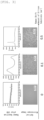
FIG. 2 is a graph illustrating a Raman peak of diamond on a silicon substrate. -
FIG. 3 is a view illustrating a relation between a Raman shift amount of a peak at 520 cm-1 of a silicon substrate and a diamond growth. -
FIG. 4 is a view illustrating a relation between an AFM roughness of a silicon substrate and a diamond growth. -
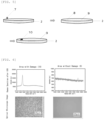
FIG. 5 is a flowchart illustrating an example of a selective diamond growth flow on a silicon substrate. -
FIG. 6 is a figure illustrating Raman spectra and optical microscope images after a CVD growth on a partially polished silicon substrate. -
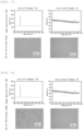
FIG. 7 is a figure illustrating Raman spectra and optical microscope images after a CVD growth on a partially dry-etched silicon substrate. -
FIG. 8 is a figure illustrating another example of Raman spectra and optical microscope images after a CVD growth on a partially dry-etched silicon substrate. - As described above, it is desired to develop a method for growing a diamond on a silicon substrate that can suppress contamination and particles.
- To solve the above problem, the present inventors have earnestly studied and found that diamond can be grown on a silicon substrate while suppressing contamination and particles by subjecting a surface of the silicon substrate to damage, or forming unevenness, or both above treatments. This led to the completion of the present invention.
- That is, the present invention is a method for growing diamond on a silicon substrate, the method includes subjecting a surface of the silicon substrate to damage as a pretreatment so as to make a Raman shift of a peak at 520 cm-1 in Raman spectroscopy 0.1 cm-1 or more, or subjecting the surface of the silicon substrate to unevenness formation as the pretreatment so as to make a surface roughness Sa measured by
AFM 10 nm or more, or subjecting the surface of the silicon substrate to both the damage and the unevenness formation thereon as the pretreatment, and growing diamond by a CVD method on the silicon substrate subjected to the pretreatment. - In this case, the pretreatment may be performed on an entire surface of the silicon substrate or a part of a region.
- Hereinafter, the present invention will be described in detail. However, the present invention is not limited thereto. The embodiments of the present invention will be described with reference to the drawings.
- The inventive method for growing diamond on a silicon substrate includes a method for growing diamond on a silicon substrate, the method includes: subjecting a surface of the silicon substrate to damage as a pretreatment so as to make a Raman shift of a peak at 520 cm-1 in Raman spectroscopy 0.1 cm-1 or more, or subjecting the surface of the silicon substrate to unevenness formation as the pretreatment so as to make a surface roughness Sa measured by
AFM 10 nm or more, or subjecting the surface of the silicon substrate to both the damage and the unevenness formation thereon as the pretreatment, and growing diamond by a CVD method on the silicon substrate subjected to the pretreatment. - In this event, it is preferred that the CVD method is a hot filament method.
-
FIG. 1 shows an example of an embodiment and schematically shows a method for growing diamond using a hot filament method. Methane and hydrogen are introduced into areaction vessel 1 as areaction gas 4, and atungsten filament 3 installed above the silicon substrate (to be film-formed substrate) 2 is energized to electric-heat and then decompose thereaction gas 4, thereby growing diamond on thesilicon substrate 2. A nucleation on the silicon substrate at this time is described. When a normal silicon substrate is measured by Raman spectroscopy, a peak at 520 cm-1 is obtained. When this silicon substrate is subjected to damage, this peak shifts. As for the change of Raman peak when scratched, for example,Non Patent Document 1 discloses a comparison between a depth (degree) of a scratch and Raman, showing that the peak at 520 cm-1 shifts as the degree of the scratch becomes larger (more severe). - As for a method for subjecting the silicon substrate surface to the damage, for example, a method for grinding the silicon substrate surface with a grindstone can be mentioned. In addition, for a method for subjecting the silicon substrate surface to the roughness, for example, a method for grinding the silicon substrate surface with a grindstone can be mentioned. A method includes immersing the substrate in pure water with diamond particles dispersed therein and applying ultrasonic waves to damage or roughen the surface. Moreover, other than such methods for mechanical damaging or roughening, for example, a method for using DC plasma (applying high voltage to the substrate and ionizing gases such as Ar or methane with plasma) to subject damage by ion particles is also available.
- In this way, the damage on the surface can be evaluated by the Raman shift; samples are produced by changing the amount of the Raman shift, and then a diamond growth is performed by the hot filament method, resulting in the diamond growth is confirmed at a place where the amount of the Raman shift of 0.1 cm-1 or more, preferably 0.5 cm-1 or more as shown in
FIG. 3 , that is, at a place where the damage becomes larger. The upper limit of the Raman shift is not particularly limited but can be, for example, defined as 2 cm-1 or less. - At this point, the growth of the diamond is confirmed by performing a Raman measurement and a resulting peak thereof at 1330 cm-1 and an optical microscope image. For example, as shown in
FIG. 2 , whenRaman peak 5 of the diamond is confirmed in the vicinity of 1330 cm-1, the growth of the diamond is indicated. Note that, in the vicinity of 1600cm-1,Raman peak 6 of carbide (graphite) can be confirmed. - In a schematic view of the method for growing diamond using the hot filament method (
FIG. 1 ), methane and hydrogen are introduced into thereaction vessel 1 as thereaction gas 4, and thetungsten filament 3 installed above thesilicon substrate 2 is energized to electric-heat and then decompose thereaction gas 4, thereby growing diamond on thesilicon substrate 2. As the nucleation to thesilicon substrate 2 at this time, samples are produced by changing surface roughness Sa measured by AFM of thesilicon substrate 2. Then, the diamond growth is performed by the hot filament method, and then the growth of the diamond can be confirmed when the surface roughness Sa is 10 nm or more and 50 nm or more, as shown inFIG. 4 . At this point, the growth of the diamond is confirmed by performing a Raman measurement and a resulting peak thereof at 1330 cm-1 and the optical microscope image. The upper limit of the surface roughness Sa is not particularly limited but can be, for example, 5000 nm or less. - The AFM measurement can be performed, for example, by XE-WAFER manufactured by Park Systems Corp.
- In a schematic view of the method for growing diamond using the hot filament method (
FIG. 1 ), methane and hydrogen are introduced into thereaction vessel 1 as thereaction gas 4, and thetungsten filament 3 installed above thesilicon substrate 2 is energized to electric-heat and then decompose thereaction gas 4, thereby growing diamond on thesilicon substrate 2. As the nucleation (pretreatment) to thesilicon substrate 2 at this time, samples are produced by changing the amount of Raman shift and the surface roughness Sa measured by AFM of thesilicon substrate 2. Subsequently, with performing the diamond growth by the hot filament method, the growth of the diamond can be confirmed at an area where the Raman shift amount is 0.1 cm-1 or more, preferably 0.5 cm-1 or more when the Raman measurement of a peak at 520 cm-1 is measured on the surface of thesilicon substrate 2, that is, at the area where the damage is larger, and the surface roughness Sa of thesilicon substrate 2 measured by AFM is 10 nm or more and 50 nm or more. In this case, the growth of the diamond is confirmed by performing the Raman measurement and a resulting peak at 1330 cm-1 and the optical microscope image. - Meanwhile, the present invention is a method for selectively growing diamond on a silicon substrate, the method includes, in the method for growing diamond on a silicon substrate described above, subjecting only a part of a region on the surface of the silicon substrate to the damage as a pretreatment, or subjecting only a part of a region on the surface of the silicon substrate to the unevenness formation as the pretreatment, or subjecting only a part of the surface of the silicon substrate to both the damage and the unevenness formation as the pretreatment, and growing diamond by a CVD method on the region where the pretreatment is performed.
- In this case, it is preferred that the CVD method is a hot filament method.
- As described above, damage on a surface can be evaluated by Raman shift. Samples of silicon substrates on which an amount of Raman shift is partially changed are produced (
FIG. 5 ), and then a diamond growth method is performed by a hot filament method, as a result, where the Raman shift amount is 0.1 cm-1 or more, i.e., at an area where damage is larger, a partially selective growth of diamond can be confirmed. InFIG. 5 , to begin with, apad portion 7 of a partial polishing apparatus is applied on thesilicon substrate 2 to produce a polished-to-roughenarea 8 and anunpolished area 9. Then, a CVD-growndiamond 10 is produced on the polished-to-roughenarea 8. - At this point, the growth of the diamond is confirmed by performing a Raman measurement and a resulting peak thereof at 1330 cm-1 and an optical microscope image.
- As for a method for partially subjecting the surface to the damage, for example, it is possible to polish (grind) only a predetermined area by a partially polishing (grinding) apparatus, or as another method, it is possible to perform photolithography and then perform a method for performing wet or dry etching, etc.
- In a schematic view of the method for growing diamond using the hot filament method (
FIG. 1 ), methane and hydrogen are introduced into areaction vessel 1 as areaction gas 4, and atungsten filament 3 installed above asilicon substrate 2 is energized to electric-heat and then decompose thereaction gas 4, thereby growing diamond on thesilicon substrate 2. As the nucleation (pretreatment) to thesilicon substrate 2 at this time, samples are produced by partially changing surface roughness Sa measured by AFM of thesilicon substrate 2. Then, the diamond growth is performed by the hot filament method, and then the partially selective growth of the diamond can be confirmed (FIG. 5 ) when the surface roughness Sa is 10 nm or more. At this point, the growth of the diamond is confirmed by performing a Raman measurement and a resulting peak thereof at 1330 cm-1 and an optical microscope image. - As for a method for partially subjecting the surface to the roughness, for example, it is possible to polish (grind) only a predetermined area by the partially polishing (grinding) apparatus, or as another method, a method for performing photolithography and then performing wet or dry etching, etc. can be selected.
- In a schematic view of the method for growing diamond using the hot filament method (
FIG. 1 ), the methane and the hydrogen are introduced into thereaction vessel 1 as thereaction gas 4, and thetungsten filament 3 installed above thesilicon substrate 2 is energized to electric-heat and then decompose thereaction gas 4, thereby growing diamond on thesilicon substrate 2. As the nucleation to thesilicon substrate 2 at this time, samples are produced by changing the amount of Raman shift and the surface roughness Sa measured by AFM of thesilicon substrate 2. Subsequently, with performing the diamond growth by the hot filament method, the partially selective growth of the diamond can be confirmed at an area where the Raman shift amount is 0.1 cm-1 or more, preferably 0.5 cm-1 or more when the Raman measurement of a peak at 520 cm-1 is measured on the surface; that is, at the area where the damage is larger, and the surface roughness Sa of thesilicon substrate 2 measured by AFM is 10 nm or more and 50 nm or more (FIG. 5 ). In this case, the growth of the diamond is confirmed by performing a Raman measurement and a resulting peak thereof at 1330 cm-1 and an optical microscope image. - As for a method for partially subjecting the surface to the damage and roughness, for example, it is possible to polish (grind) only a predetermined area by the partially polishing (grinding) apparatus, or as another method, a method for performing photolithography and then performing wet or dry etching, etc. can be selected.
- Hereinafter, the present invention will be specifically described with reference to Examples and Comparative Examples. However, the present invention is not limited thereto.
- A boron-doped high resistance single crystal silicon substrate having a diameter of 300 mm and orientation (111) was provided, and then three types of substrates having different surface conditions were provided in which an intact substrate (CMP processed), ground by a grindstone of 12000 grit, and ground by a grindstone of 3000 grit. Raman measurements were performed to respective substrate surfaces to evaluate a peak shift of silicon from 520 cm-1; that of the CMP processed substrate had a shift amount of 0 cm-1, that of 12000 grit ground had 0.1 cm-1, that of 3000 grit ground had 0.5 cm-1.
- Each of these substrates was placed in a hot filament CVD apparatus and grown for 4 hours under the following conditions: a filament temperature: 2200°C, an H2 flow rate: 10 SLM, a CH4 concentration: 3 %, a substrate temperature: 850°C, 5 Torr (667 Pa). The Raman measurements were then performed to evaluate diamond growth. As a result, a relationship between a Raman shift amount of the silicon substrate and the diamond growth was observed, with no diamond growth observed when the Raman shift amount of the silicon substrate was 0 cm-1, but the diamond growth was observed when the Raman shift was 0.1 cm-1 or more (
FIG. 3 ) . - A boron-doped high resistance single crystal silicon substrate having a diameter of 300 mm and orientation (111) was provided, and then three types of substrates having different surface conditions were provided in which an intact substrate (CMP processed), ground by a grindstone of 12000 grit, and ground by a grindstone of 3000 grit. When roughness measurement on each substrate surface by AFM was performed, a roughness Sa of the CMP processed substrate was 1 nm, that of 12000 grit ground was 10 nm, and that of 3000 grit ground was 50 nm. However, due to the unreliability of AFM for Sa = 50 nm (3000 grit), the results were also confirmed with a visual field of 100 um using a white-light interference microscope.
- Each of these substrates was placed in a hot filament CVD apparatus and grown for 4 hours under the following conditions: a filament temperature: 2200°C, an H2 flow rate: 10 SLM, a CH4 concentration: 3 %, a substrate temperature: 850°C, 5 Torr (667 Pa). Raman measurements were then performed to evaluate a diamond growth. As a result, a relationship between the surface roughness Sa of the silicon substrate and the diamond growth was observed, with no diamond growth observed when the surface roughness Sa of the silicon substrate was 1 nm, but the diamond growth was observed when the surface roughness Sa was 10 nm or more (
FIG. 4 ). - A boron-doped high resistance single crystal silicon substrate having a diameter of 300 mm and orientation (111) was provided, and then a surface thereof was ground by a small grindstone of 12000 grit using a partially polishing apparatus to perform Raman measurement of the substrate surface; then, a sample in which a peak shift amount of silicon from 520 cm-1 was 0.1 cm-1 was provided.
- This substrate was placed in a hot filament CVD apparatus and grown for 4 hours under the following conditions: a filament temperature: 2200°C, an H2 flow rate: 10 SLM, a CH4 concentration: 3 %, a substrate temperature: 850°C, 5 Torr (667 Pa). The Raman measurement was then performed to evaluate a diamond growth. As a result, the diamond growth was observed only in the partially ground area on the silicon substrate (
FIG. 6 ). - A boron-doped high resistance single crystal silicon substrate having a diameter of 300 mm and orientation (111) was provided, and then a surface thereof was ground by a small grindstone of 12000 grit using a partially polishing apparatus to perform a roughness measurement by AFM of the substrate surface, then the surface roughness Sa was 10 nm.
- This substrate was placed in a hot filament CVD apparatus and grown for 4 hours under the following conditions: a filament temperature: 2200°C, an H2 flow rate: 10 SLM, a CH4 concentration: 3 %, a substrate temperature: 850°C, 5 Torr (667 Pa). The Raman measurement was then performed to evaluate a diamond growth. As a result, the diamond growth was observed only in the partially ground area on the silicon substrate (
FIG. 6 ). - A boron-doped high resistance single crystal silicon substrate having a diameter of 300 mm and orientation (111) was provided, photolithography was then performed thereon to form a window only in a predetermined area, and then the substrate was etched in a plasma etching apparatus for 5 minutes under conditions of a flow rate of 100 sscm and 100 Torr (13332 Pa) using CF4 as an etching gas. Then, a resist was removed by oxygen plasma to measure roughness and damage by Raman and AFM. As a result, the roughness Sa by AFM was 15 nm, and a peak shift amount at 520 cm-1 in the Raman spectrum was 1 cm-1.
- This substrate was placed in a hot filament CVD apparatus and grown for 4 hours under the following conditions: a filament temperature: 2200°C, an H2 flow rate: 10 SLM, a CH4 concentration: 3 %, a substrate temperature: 850°C, 5 Torr (667 Pa). The Raman measurement was then performed to evaluate a diamond growth. As a result, the diamond growth was observed only in the partially ground area on the silicon substrate (
FIG. 7 ). - A boron-doped high resistance single crystal silicon substrate having a diameter of 300 mm and orientation (111) was provided, and the substrate was oxidized to form a silicon oxide film of 100 nm, and then photolithography was performed to form a window to the oxide film only in a predetermined area. Subsequently, etching was performed with 10 % KOH aqueous solution for 5 min. The oxide film was then removed with buffered HF, and roughness and damage were measured by Raman and AFM. As a result, the roughness Sa by AFM was 50 nm, and a peak shift amount at 520 cm-1 in the Raman spectrum was 1.2 cm-1.
- This substrate was placed in a hot filament CVD apparatus and grown for 4 hours under the following conditions: a filament temperature: 2200°C, an H2 flow rate: 10 SLM, a CH4 concentration: 3 %, a substrate temperature: 850°C, 5 Torr (667 Pa). The Raman measurement was then performed to evaluate a diamond growth. As a result, the diamond growth was observed only in the partially ground area on the silicon substrate (
FIG. 8 ). - It should be noted that the present invention is not limited to the above-described embodiments. The embodiments are just examples, and any examples that have substantially the same feature and demonstrate the same functions and effects as those in the technical concept disclosed in claims of the present invention are included in the technical scope of the present invention.
Claims (4)
- A method for growing diamond on a silicon substrate, the method comprising:subjecting a surface of a silicon substrate to damage as a pretreatment so as to make a Raman shift of a peak at 520 cm-1 in Raman spectroscopy 0.1 cm-1 or more;or subjecting the surface of the silicon substrate to unevenness formation as the pretreatment so as to make a surface roughness Sa measured by AFM 10 nm or more;or subjecting the surface of the silicon substrate to both the damage and the unevenness formation thereon as the pretreatment; andgrowing diamond by a CVD method on the silicon substrate subjected to the pretreatment.
- The method for growing diamond on a silicon substrate according to claim 1, wherein
the CVD method is a hot filament method. - A method for selectively growing diamond on a silicon substrate, the method comprising:in the method for growing diamond on a silicon substrate according to claim 1,subjecting only a part of a region on the surface of the silicon substrate to the damage as a pretreatment,or subjecting only a part of a region on the surface of the silicon substrate to the unevenness formation as the pretreatment,or subjecting only a part of the surface of the silicon substrate to both the damage and the unevenness formation as the pretreatment; andgrowing diamond by a CVD method on the region where the pretreatment is performed.
- The method for selectively growing diamond on a silicon substrate according to claim 3, wherein
the CVD method is a hot filament method.
Applications Claiming Priority (2)
| Application Number | Priority Date | Filing Date | Title |
|---|---|---|---|
| JP2022020997A JP7432119B2 (en) | 2022-02-15 | 2022-02-15 | Method for growing diamond on a silicon substrate and method for selectively growing diamond on a silicon substrate |
| PCT/JP2023/002500 WO2023157599A1 (en) | 2022-02-15 | 2023-01-26 | Method for growing diamond on silicon substrate and method for selectively growing diamond on silicon substrate |
Publications (2)
| Publication Number | Publication Date |
|---|---|
| EP4481796A1 true EP4481796A1 (en) | 2024-12-25 |
| EP4481796A4 EP4481796A4 (en) | 2025-10-22 |
Family
ID=87578394
Family Applications (1)
| Application Number | Title | Priority Date | Filing Date |
|---|---|---|---|
| EP23756127.9A Pending EP4481796A4 (en) | 2022-02-15 | 2023-01-26 | Method for growing diamond on a silicon substrate and method for selectively growing diamond on a silicon substrate |
Country Status (7)
| Country | Link |
|---|---|
| US (1) | US20250109488A1 (en) |
| EP (1) | EP4481796A4 (en) |
| JP (1) | JP7432119B2 (en) |
| KR (1) | KR20240145997A (en) |
| CN (1) | CN118591869A (en) |
| TW (1) | TW202348553A (en) |
| WO (1) | WO2023157599A1 (en) |
Family Cites Families (8)
| Publication number | Priority date | Publication date | Assignee | Title |
|---|---|---|---|---|
| JP2637508B2 (en) * | 1988-02-08 | 1997-08-06 | キヤノン株式会社 | Method for forming vapor-phase synthetic diamond crystal and substrate having diamond crystal |
| JP3185289B2 (en) * | 1991-12-03 | 2001-07-09 | ソニー株式会社 | Diamond deposition method |
| JPH06263595A (en) * | 1993-03-10 | 1994-09-20 | Canon Inc | Diamond-coated material and its production |
| JP2001354491A (en) | 2000-06-07 | 2001-12-25 | New Japan Radio Co Ltd | Method and device for growing diamond |
| JP2004176132A (en) | 2002-11-27 | 2004-06-24 | Toppan Printing Co Ltd | Nanodiamond film and method of manufacturing the same |
| JP2006143561A (en) | 2004-11-24 | 2006-06-08 | Japan Science & Technology Agency | Low temperature synthesis method of diamond |
| JP2009091234A (en) | 2007-09-18 | 2009-04-30 | Tokyo Univ Of Science | Substrate on which conductive diamond film is formed and method for manufacturing substrate on which conductive diamond film is formed |
| WO2019226850A1 (en) | 2018-05-25 | 2019-11-28 | The Government Of The United States Of America, As Represented By The Secretary Of The Navy | Diamond on nanopatterned substrate |
-
2022
- 2022-02-15 JP JP2022020997A patent/JP7432119B2/en active Active
-
2023
- 2023-01-26 KR KR1020247026455A patent/KR20240145997A/en active Pending
- 2023-01-26 CN CN202380019505.XA patent/CN118591869A/en active Pending
- 2023-01-26 EP EP23756127.9A patent/EP4481796A4/en active Pending
- 2023-01-26 WO PCT/JP2023/002500 patent/WO2023157599A1/en not_active Ceased
- 2023-01-26 US US18/832,814 patent/US20250109488A1/en active Pending
- 2023-02-01 TW TW112103426A patent/TW202348553A/en unknown
Also Published As
| Publication number | Publication date |
|---|---|
| US20250109488A1 (en) | 2025-04-03 |
| EP4481796A4 (en) | 2025-10-22 |
| TW202348553A (en) | 2023-12-16 |
| WO2023157599A1 (en) | 2023-08-24 |
| JP2023118186A (en) | 2023-08-25 |
| KR20240145997A (en) | 2024-10-07 |
| JP7432119B2 (en) | 2024-02-16 |
| CN118591869A (en) | 2024-09-03 |
Similar Documents
| Publication | Publication Date | Title |
|---|---|---|
| EP3042389B1 (en) | Semiconductor device structures comprising polycrystalline cvd diamond with improved near-substrate thermal conductivity | |
| Zhang et al. | Highly efficient and damage-free polishing of GaN (0 0 0 1) by electrochemical etching-enhanced CMP process | |
| Shi et al. | Characterization of colloidal silica abrasives with different sizes and their chemical–mechanical polishing performance on 4H-SiC (0 0 0 1) | |
| US5458733A (en) | Method for etching a diamond film | |
| JP3292101B2 (en) | Method for smoothing silicon single crystal substrate surface | |
| Stubhan et al. | Heteroepitaxial nucleation of diamond on Si (001) in hot filament chemical vapor deposition | |
| Nugera et al. | Effect of CH4 concentration on the early growth stage of patterned diamond using high seeding density and hot filament chemical vapor deposition | |
| Rotter et al. | Diamond CVD by a combined plasma pretreatment and seeding procedure | |
| WO1992022689A1 (en) | Process for making large-area single crystal diamond films | |
| US20250109488A1 (en) | Method for growing diamond on silicon substrate and method for selectively growing diamond on silicon substrate | |
| Huang et al. | Growth of diamond films with high surface smoothness | |
| JP5124781B2 (en) | Nano-diamond thin film having n-type conductivity and method for producing the same | |
| Wang et al. | CVD diamond nucleation enhanced by ultrasonic pretreatment using diamond and mixture of diamond and TaC powders | |
| Feygelson et al. | Reduced-stress nanocrystalline diamond films for heat spreading in electronic devices | |
| Tao et al. | High-efficiency modification mechanism of GaN (0001) in plasma-assisted polishing using hydrogen plasma | |
| Ali et al. | Effect of surface treatment on hot-filament chemical vapour deposition grown diamond films | |
| Rebello et al. | On the Effects of Physical Abrasion on Nucleation and Growth of Diamond on Silicon Using Hot Filament Chemical Vapor Deposition | |
| TWI490064B (en) | Micro-drill and method for manufacturing the same | |
| Ali et al. | Diamond films grown without seeding treatment and bias by hot-filament CVD system | |
| Wang et al. | High‐Quality Silicon‐Based Diamond Growth Based on a Femtosecond Laser‐Induced Diamond Nucleation | |
| Trava-Airoldi et al. | CVD-Diamond: an overview of research and development at INPE | |
| Shen et al. | Enhanced diamond nucleation on pretreated silicon substrates | |
| Pryor et al. | Growth technique for large area mosaic diamond films | |
| Hayashi et al. | Role of cyclic process in the initial stage of diamond deposition during bias enhanced nucleation | |
| Pryor et al. | MOSAIC DIAMOND FILMSt |
Legal Events
| Date | Code | Title | Description |
|---|---|---|---|
| STAA | Information on the status of an ep patent application or granted ep patent |
Free format text: STATUS: THE INTERNATIONAL PUBLICATION HAS BEEN MADE |
|
| PUAI | Public reference made under article 153(3) epc to a published international application that has entered the european phase |
Free format text: ORIGINAL CODE: 0009012 |
|
| STAA | Information on the status of an ep patent application or granted ep patent |
Free format text: STATUS: REQUEST FOR EXAMINATION WAS MADE |
|
| 17P | Request for examination filed |
Effective date: 20240712 |
|
| AK | Designated contracting states |
Kind code of ref document: A1 Designated state(s): AL AT BE BG CH CY CZ DE DK EE ES FI FR GB GR HR HU IE IS IT LI LT LU LV MC ME MK MT NL NO PL PT RO RS SE SI SK SM TR |
|
| DAV | Request for validation of the european patent (deleted) | ||
| DAX | Request for extension of the european patent (deleted) | ||
| A4 | Supplementary search report drawn up and despatched |
Effective date: 20250919 |
|
| RIC1 | Information provided on ipc code assigned before grant |
Ipc: H01L 21/314 20060101AFI20250915BHEP Ipc: C01B 32/25 20170101ALI20250915BHEP Ipc: C23C 16/27 20060101ALI20250915BHEP Ipc: C30B 25/18 20060101ALI20250915BHEP Ipc: C30B 29/04 20060101ALI20250915BHEP Ipc: H01L 21/31 20060101ALI20250915BHEP Ipc: H01L 21/02 20060101ALI20250915BHEP |