EP4481486A1 - Optical switch and switching method - Google Patents
Optical switch and switching method Download PDFInfo
- Publication number
- EP4481486A1 EP4481486A1 EP22927299.2A EP22927299A EP4481486A1 EP 4481486 A1 EP4481486 A1 EP 4481486A1 EP 22927299 A EP22927299 A EP 22927299A EP 4481486 A1 EP4481486 A1 EP 4481486A1
- Authority
- EP
- European Patent Office
- Prior art keywords
- signal light
- optical
- modulation element
- signal
- mirror
- Prior art date
- Legal status (The legal status is an assumption and is not a legal conclusion. Google has not performed a legal analysis and makes no representation as to the accuracy of the status listed.)
- Pending
Links
Images



Classifications
-
- G—PHYSICS
- G02—OPTICS
- G02F—OPTICAL DEVICES OR ARRANGEMENTS FOR THE CONTROL OF LIGHT BY MODIFICATION OF THE OPTICAL PROPERTIES OF THE MEDIA OF THE ELEMENTS INVOLVED THEREIN; NON-LINEAR OPTICS; FREQUENCY-CHANGING OF LIGHT; OPTICAL LOGIC ELEMENTS; OPTICAL ANALOGUE/DIGITAL CONVERTERS
- G02F1/00—Devices or arrangements for the control of the intensity, colour, phase, polarisation or direction of light arriving from an independent light source, e.g. switching, gating or modulating; Non-linear optics
- G02F1/29—Devices or arrangements for the control of the intensity, colour, phase, polarisation or direction of light arriving from an independent light source, e.g. switching, gating or modulating; Non-linear optics for the control of the position or the direction of light beams, i.e. deflection
- G02F1/31—Digital deflection, i.e. optical switching
-
- G—PHYSICS
- G02—OPTICS
- G02F—OPTICAL DEVICES OR ARRANGEMENTS FOR THE CONTROL OF LIGHT BY MODIFICATION OF THE OPTICAL PROPERTIES OF THE MEDIA OF THE ELEMENTS INVOLVED THEREIN; NON-LINEAR OPTICS; FREQUENCY-CHANGING OF LIGHT; OPTICAL LOGIC ELEMENTS; OPTICAL ANALOGUE/DIGITAL CONVERTERS
- G02F1/00—Devices or arrangements for the control of the intensity, colour, phase, polarisation or direction of light arriving from an independent light source, e.g. switching, gating or modulating; Non-linear optics
- G02F1/29—Devices or arrangements for the control of the intensity, colour, phase, polarisation or direction of light arriving from an independent light source, e.g. switching, gating or modulating; Non-linear optics for the control of the position or the direction of light beams, i.e. deflection
- G02F1/31—Digital deflection, i.e. optical switching
- G02F1/315—Digital deflection, i.e. optical switching based on the use of controlled internal reflection
-
- H—ELECTRICITY
- H04—ELECTRIC COMMUNICATION TECHNIQUE
- H04Q—SELECTING
- H04Q11/00—Selecting arrangements for multiplex systems
- H04Q11/0001—Selecting arrangements for multiplex systems using optical switching
- H04Q11/0005—Switch and router aspects
-
- G—PHYSICS
- G02—OPTICS
- G02F—OPTICAL DEVICES OR ARRANGEMENTS FOR THE CONTROL OF LIGHT BY MODIFICATION OF THE OPTICAL PROPERTIES OF THE MEDIA OF THE ELEMENTS INVOLVED THEREIN; NON-LINEAR OPTICS; FREQUENCY-CHANGING OF LIGHT; OPTICAL LOGIC ELEMENTS; OPTICAL ANALOGUE/DIGITAL CONVERTERS
- G02F2203/00—Function characteristic
- G02F2203/50—Phase-only modulation
-
- H—ELECTRICITY
- H04—ELECTRIC COMMUNICATION TECHNIQUE
- H04Q—SELECTING
- H04Q11/00—Selecting arrangements for multiplex systems
- H04Q11/0001—Selecting arrangements for multiplex systems using optical switching
- H04Q11/0005—Switch and router aspects
- H04Q2011/0007—Construction
- H04Q2011/0026—Construction using free space propagation (e.g. lenses, mirrors)
-
- H—ELECTRICITY
- H04—ELECTRIC COMMUNICATION TECHNIQUE
- H04Q—SELECTING
- H04Q11/00—Selecting arrangements for multiplex systems
- H04Q11/0001—Selecting arrangements for multiplex systems using optical switching
- H04Q11/0005—Switch and router aspects
- H04Q2011/0037—Operation
- H04Q2011/0041—Optical control
Definitions
- the present invention relates to an optical switch and a switching method each of which switches an optical path of signal light from one to another.
- optical trunk line network With increasing data traffic, the demand for increased capacity in optical trunk line networks is increasing. In order to respond to this demand, the form of the optical trunk line network is developed from the point-to-point type to the ring type, and then to the mesh type. For efficient use of the mesh-type optical trunk line network, it is necessary to quickly switch the path of the signal light from one to another.
- Known optical switches capable of quickly switching the path of the signal light from one to another include an optical switch using a digital mirror device (DMD) and an optical switch using a liquid crystal on silicon (LCOS).
- DMD digital mirror device
- LCOS liquid crystal on silicon
- Patent Literature 1 discloses an optical switch using LCOS.
- Patent Literature 1 Japanese Patent Application Publication Tokukai No. 2015-94779
- An aspect of the present invention was made in consideration of the above problems, and realizes an optical switch having a function to switch an optical path of signal light from one to another according to a control signal superimposed on the signal light.
- An optical switch in accordance with an aspect of the present invention is an optical switch that switches an optical path of signal light from one to another, the signal light being obtained by modulating carrier light by a control signal and a data signal
- the optical switch including: a mirror and a half mirror; an optical modulation element configured to reflect or refract the signal light reflected by the mirror and the half mirror, the optical modulation element including a plurality of cells having phase modulation amounts settable independently of each other; a light detector configured to detect, at once, intensities of beams of the signal light having been reflected by the mirror and the half mirror different times and having passed through the half mirror; and a control section configured (a) to decode the control signal from the intensities of the beams of the signal light detected at once by the light detector and (b) to set the phase modulation amounts of the plurality of cells in the optical modulation element so that the signal light is emitted in a direction corresponding to the control signal.
- a switching method in accordance with an aspect of the present invention is a switching method that switches an optical path of signal light from one to another, the signal light being obtained by modulating carrier light by a control signal and a data signal, the switching method including the steps of: reflecting or refracting, with use of an optical modulation element, the signal light reflected by a mirror and a half mirror, the optical modulation element including a plurality of cells having phase modulation amounts settable independently of each other; detecting, at once, intensities beams of the signal light having been reflected by the mirror and the half mirror different times and having passed through the half mirror; and decoding the control signal from the intensities of the beams of the signal light detected at once and setting the phase modulation amounts of the plurality of cells in the optical modulation element so that the signal light is emitted in a direction corresponding to the control signal.
- An optical switch 1 is a device that switches an optical path of signal light L from one to another.
- the signal light L is obtained by modulating carrier light L0 by a control signal C and a data signal D.
- the control signal C has a bit rate of 1/Tc
- the data signal has a bit rate of 1/Td. That is, the signal light L is modulated by one-bit control signal C per Tc seconds and is modulated by one-bit data signal D per Td seconds.
- the control signal C designates an optical path of the signal light L.
- the control signal C designates one optical path per n bit (n is any natural number of not less than 1).
- Fig. 1 shows waveform charts illustrating, as an example, waveforms of signal light L1.
- (a) of Fig. 1 shows a waveform chart illustrating, as an example, a waveform of carrier light L0.
- (b) of Fig. 1 shows a waveform chart illustrating, as an example, a waveform of signal light L' obtained by modulating the carrier light L0 by the control signal C.
- (c) of Fig. 1 shows a waveform chart illustrating, as an example, a waveform of the signal light L obtained by modulating the signal light L' by the data signal D.
- n 3.
- the control signal C designates one optical path per 3 bits.
- an optical path of the signal light L1 in which the first bit of the data signal D (which may also be referred to as a "data signal D1”) is modulated is designated by first three bits of the control signal C (which may also be referred to as a "control signal C1")
- an optical path of the signal light L2 in which subsequent one bit of the data signal D (which may also be referred to as a "data signal D2") is modulated is designated by subsequent three bits of the control signal C (which may also be referred to as a "control signal C2").
- the order of the processes for modulation is not limited to the one shown in Fig. 1 .
- a configuration in which the carrier light L0 is modulated by the control signal C and then by the data signal D may be employed.
- the modulation may be carried out with use of an optical modulator or a multiplexer. In the latter case, for example, it is possible to generate signal light L' by multiplexing signal light Lc indicative of the control signal C into the carrier light L0, and it is possible to generate signal light L by multiplexing signal light Ld indicative of the data signal D into the signal light L'.
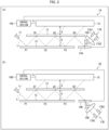
- FIG. 2 shows a side view illustrating a configuration example of a reflective optical switch 1.
- the reflective optical switch 1 may also be referred to as an optical switch 1A.
- the optical switch 1A includes an input port 11, a mirror 12, a half mirror 13, an optical modulation element 14A, a light detector 15, a control section 16A, an output port group 17A, and a lens 18A.
- the input port 11 is a means that guides signal light Li which is to be input into the optical switch 1A.
- the present embodiment uses an optical fiber as the input port 11.
- the signal light Li emitted from the input port 11 enters the mirror 12.
- the mirror 12 is a means that reflects the signal light Li having entered the mirror 12.
- the half mirror 13 is a means that reflects a portion of the signal light Li having entered the half mirror 13 and allows a portion of the signal light Li having entered the half mirror 13 to pass therethrough.
- the mirror 12 and the half mirror 13 are disposed so that their respective reflecting surfaces face each other.
- the signal light Li having entered the mirror 12 (1) is reflected by a point P1 in the mirror 12, (2) is reflected by a point Q1 in the half mirror 13, (3) is reflected by a point P2 in the mirror 12, (4) is reflected by a point Q2 in the half mirror 13, (5) is reflected by a point P3 in the mirror 12, and (6) is reflected by a point Q3 in the half mirror 13.
- the signal light Li having reflected by the point Q3 in the half mirror 13 enters the optical modulation element 14A.
- the signal light Li having passed through the points Q1, Q2, and Q3 in the half mirror 13 enters the light detector 15.
- a distance d between the mirror 12 and the half mirror 13 is set so that a period of time from (i) reflection of the signal light Li by the half mirror 13 to (ii) re-entry of the signal light Li into the half mirror 13 is Tc.
- the distance d is set so that an optical path length of the signal light Li from a point Qi (i is a natural number of not less than 1 and not more than n-1), through a point Pi+ 1, to a point Qi+ 1 is c ⁇ Tc (c is a speed of light).
- the optical modulation element 14A is a means that modulates and reflects the signal light Li, and is constituted by a plurality of cells having phase modulation amounts settable independently of each other.
- the optical modulation element 14A may sometimes be called a "spatial optical modulator". A configuration example of the optical modulation element 14A will be described later with reference to a different drawing.
- the phase modulation amounts of the cells constituting the optical modulation element 14A are controlled by the control section 16A so that the signal light Li is emitted in a direction corresponding to the control signal Ci.
- the light detector 15 is a means that detects, at once, beams of signal light Li having been reflected by the mirror 12 and the half mirror 13 different times and having passed through the half mirror 13.
- the light detector 15 is a means that detects, as a spatial distribution of intensities of the beams of the signal light Li having passed through the half mirror 13, changes over time in the intensity of the signal light Li.
- the present embodiment uses an image sensor as the light detector 15.
- the light detector 15 detects, at once, (1) the signal light Li having passed through the point Q3 in the half mirror 13 and having been modulated by the first bit of the control signal Ci, (2) the signal light Li having passed through the point Q2 in the half mirror 13 and having been modulated by the second bit of the control signal Ci, and (3) the signal light Li having passed through the point Q3 in the half mirror 13 and having been modulated by the third bit of the control signal Ci.
- the intensities of the beams of the signal light Li detected by the light detector 15 are provided to the control section 16A.
- the present embodiment employs a configuration in which the light detector 15 detects, at once, intensities of a beam of the signal light Li reflected by the mirror 12 once, a beam of the signal light Li reflected by the mirror 12 twice, and a beam of the signal light Li reflected by the mirror 12 three times.
- the present invention is not limited to this configuration.
- the light detector 15 detects, at once, intensities of a beam of the signal light Li not reflected by the mirror 12, a beam of the signal light Li reflected by the mirror 12 once, and a beam of the signal light Li reflected by the mirror 12 twice.
- the light detector 15 detects, at once, intensities of a beam of the signal light Li reflected by the mirror 12 m times, a beam of the signal light Li reflected by the mirror 12 m+1 times, ... , and a beam of the signal light reflected by the mirror 12 m+n times, where m is any integer of not less than 0.
- the control section 16A is a means that (a) decodes the control signal Ci from the intensities of the beams of the signal light Li detected by the light detector 15 and (b) sets the phase modulation amounts of the cells in the optical modulation element 14A so that the signal light Li is reflected in a direction corresponding to the control signal Ci thus decoded.
- the control section 16A sets the phase modulation amounts of the cells in the optical modulation element 14A so that the signal light Li is reflected in a direction in which an emission angle thereof is ⁇ 1.
- the control section 16A sets the phase modulation amounts of the cells in the optical modulation element 14A so that the signal light Li is reflected in a direction in which an emission angle thereof is ⁇ 2.
- the output port group 17A is constituted by a plurality of output ports 17A1 and 17A2.
- Each of the output ports 17A1 and 17A2 is a means that guides the signal light Li to be output from the optical switch 1A.
- the present embodiment uses an optical fiber as each of the output ports 17A1 and 17A2.
- the output port 17A1 is disposed on an optical path of the signal light Li reflected by the optical modulation element 14A so that the emission angle thereof is ⁇ 1.
- the control signal Ci is 101
- the signal light Li reflected by the optical modulation element 14A enters the output port 17A1 and then is guided through the output port 17A1.
- the output port 17A2 is disposed on an optical path of the signal light Li reflected by the optical modulation element 14A so that the emission angle thereof is ⁇ 2.
- the control signal Ci is 010
- the signal light Li reflected by the optical modulation element 14A enters the output port 17A2 and then is guided through the output port 17A2.
- the lens 18A is a means that collects the signal light Li reflected by the optical modulation element 14A.
- the lens 18A collects, into an entrance end surface of the output port 17A1, the signal light Li reflected by the optical modulation element 14A so that the emission angle thereof is ⁇ 1. Further, the lens 18A collects, into an entrance end surface of the output port 17A2, the signal light Li reflected by the optical modulation element 14A so that the emission angle thereof is ⁇ 2.
- Providing the lens 18A makes it possible to cause the signal light Li reflected by the optical modulation element 14A to efficiently enter the output ports 17A1 and 17A2.
- the mirror 12 may be realized by an optical modulation element.
- a region of a portion of the optical modulation element may be used as the optical modulation element 14A, and a region of the other portion of the optical modulation element may be used as the mirror 12.
- the optical switch 1A may include a plurality of sets of the input port 11 and the output port group 17A. With this, it is possible to realize a multichannel optical switch.
- a distance d' between the half mirror 13 and the light detector 15 is equal to the distance d between the mirror 12 and the half mirror 13. This makes it possible to make (i) a time when a portion of the signal light Li which portion corresponds to the head of the data signal Di reaches the optical modulation element 14A coincide with (ii) a time when portions of the signal light Li which portions respectively correspond to the heads of the first bit, the second bit, and the third bit of the control signal Ci simultaneously reach the light detector 15.
- the distance d' between the half mirror 13 and the light detector 15 may be set smaller than the distance d between the mirror 12 and the half mirror 13. Consequently, before the portion of the signal light Li which portion corresponds to the head of the data signal Di reaches the optical modulation element 14A, the portions of the signal light Li which portions respectively correspond to the heads of the first bit, the second bit, and the third bit of the control signal Ci simultaneously reach the light detector 15. Thus, it becomes easy to reflect, in a direction designated by the control signal Ci, the portion of the signal light Li which portion corresponds to the head of the data signal Di.
- FIG. 2 shows a side view illustrating a configuration example of a transmissive optical switch 1.
- the transmissive optical switch 1 may also be referred to as an optical switch 1B.
- the optical switch 1B includes an input port 11, a mirror 12, a half mirror 13, an optical modulation element 14B, a light detector 15, a control section 16B, an output port group 17B, and a lens 18B.
- the input port 11, the mirror 12, the half mirror 13, and the light detector 15 included in the optical switch 1B have similar configurations to the input port 11, the mirror 12, the half mirror 13, and the light detector 15 included in the optical switch 1A, respectively.
- the optical modulation element 14B is a means that modulates and refracts signal light Li, and is constituted by a plurality of cells having phase modulation amounts settable independently of each other.
- the optical modulation element 14B may sometimes be called a "spatial optical modulator". A configuration example of the optical modulation element 14B will be described later with reference to a different drawing.
- the phase modulation amounts of the cells constituting the optical modulation element 14B are controlled by the control section 16B so that the signal light Li is emitted in a direction corresponding to the control signal Ci.
- the control section 16B is a means that (a) decodes the control signal Ci from the intensities of the beams of the signal light Li detected by the light detector 15 and (b) sets the phase modulation amounts of the cells in the optical modulation element 14B so that the signal light Li is refracted in a direction corresponding to the control signal Ci thus decoded.
- the control section 16B sets the phase modulation amounts of the cells in the optical modulation element 14B so that the signal light Li is refracted in a direction in which an emission angle is ⁇ 1.
- the control section 16B sets the phase modulation amounts of the cells in the optical modulation element 14B so that the signal light Li is refracted in a direction in which an emission angle is ⁇ 2.
- the output port group 17B is constituted by a plurality of output ports 17B1 and 17B2.
- Each of the output ports 17B1 and 17B2 is a means that guides the signal light Li to be output from the optical switch 1B.
- the present embodiment uses an optical fiber as each of the output ports 17B1 and 17B2.
- the output port 17B1 is disposed on an optical path of the signal light Li refracted by the optical modulation element 14B so that the emission angle thereof is ⁇ 1.
- the control signal Ci is 101
- the signal light Li refracted by the optical modulation element 14B enters the output port 17B1 and then is guided through the output port 17B1.
- the output port 17B2 is disposed on an optical path of the signal light Li refracted by the optical modulation element 14B so that the emission angle thereof is ⁇ 2.
- the control signal Ci is 010
- the signal light Li refracted by the optical modulation element 14B enters the output port 17B2 and then is guided through the output port 17B2.
- the lens 18B is a means that collects the signal light Li refracted by the optical modulation element 14B.
- the lens 18B collects, into an entrance end surface of the output port 17B1, the signal light Li refracted by the optical modulation element 14B so that the emission angle thereof is ⁇ 1.
- the lens 18B collects, into an entrance end surface of the output port 17B2, the signal light Li refracted by the optical modulation element 14B so that the emission angle thereof is ⁇ 2.
- Providing the lens 18B makes it possible to cause the signal light Li refracted by the optical modulation element 14B to efficiently enter the output ports 17B1 and 17B2.
- the mirror 12 may be realized by an optical modulation element.
- a region of a portion of the optical modulation element may be used as the optical modulation element 14B, and a region of the other portion of the optical modulation element may be used as the mirror 12.
- the optical switch 1B may include a plurality of sets of the input port 11 and the output port group 17B. With this, it is possible to realize a multichannel optical switch.
- a distance d' between the half mirror 13 and the light detector 15 is equal to a distance d between the mirror 12 and the half mirror 13.
- the distance d' between the half mirror 13 and the light detector 15 may be set smaller than the distance d between the mirror 12 and the half mirror 13. Consequently, before the portion of the signal light Li which portion corresponds to the head of the data signal Di reaches the optical modulation element 14B, the portions of the signal light Li which portions respectively correspond to the heads of the first bit, the second bit, and the third bit of the control signal Ci simultaneously reach the light detector 15. Thus, it becomes easy to refract, in a direction designated by the control signal Ci, the portion of the signal light Li which portion corresponds to the head of the data signal Di.
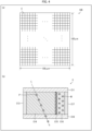
- Fig. 3 a configuration example of a reflective optical modulation element 14A included in the reflective optical switch 1A.
- (a) of Fig. 3 is a plan view of the optical modulation element 14A in accordance with the present specific example.
- (b) of Fig. 3 is a cross-sectional view of a microcell C included in the optical modulation element 14A in accordance with the present specific example.
- the optical modulation element 14A is constituted by a plurality of microcells C having phase modulation amounts set independently of each other.
- the resulting beams of the signal light Li being reflected by the microcells C while being subjected to phase modulation interfere with each other, whereby signal light Li to be emitted in a direction corresponding to the control signal Ci is formed.
- the phase modulation amount of each microcell C may be variable or fixed. In the present configuration example, the phase modulation amount of each microcell C is variable.
- the "microcell” refers to a cell having a cell size of less than 10 pm, for example.
- the "cell size” refers to a square root of an area of the cell.
- the cell size of the microcell C refers to a length of one side of the microcell C.
- a lower limit of the cell size of the microcell C is, for example, 1 nm.
- the optical modulation element 14A illustrated in (a) of Fig. 3 is constituted by 200 ⁇ 200 microcells C arranged in a matrix. Each of the microcells C has a square shape having a size of 500 nm ⁇ 500 nm in a plan view. The optical modulation element 14A has a square shape having a size of 100 pm ⁇ 100 pm in a plan view.
- Each of the microcells C constituting the optical modulation element 14A may be made of, for example, a polarizing plate C11, a reflecting plate C12, a first electrode C13, a magnetization free layer C14, an insulating layer C15, a magnetization fixed layer C16, and a second electrode C17, as shown in (b) of Fig. 3 .
- the polarizing plate C11 and the reflecting plate C12 are disposed opposite to each other.
- the first electrode C13, the magnetization free layer C14, the insulating layer C15, the magnetization fixed layer C16, and the second electrode C17 are stacked in this order, and are sandwiched between the polarizing plate C11 and the reflecting plate C12.
- a direction in which the first electrode C13, the magnetization free layer C14, the insulating layer C15, the magnetization fixed layer C16, and the second electrode C17 are stacked is orthogonal to a direction in which the polarizing plate C11 and the reflecting plate C12 are stacked.
- a first side surface of the magnetization free layer C14 is in surface contact with one main surface of the polarizing plate C11, and a second side surface of the magnetization free layer C14 which second side surface is opposite to the first side surface is in surface contact with one main surface of the reflecting plate C12.
- Signal light Li (1) enters an inside of the magnetization free layer C14 through the polarizing plate C11, (2) is reflected by the reflecting plate C12, and (3) is emitted through the polarizing plate C11 to an outside of the magnetization free layer C14.
- the magnetization free layer C14 is made of, for example, an electrically conductive, light-transmissive, soft magnetic material (for example, CoFeB).
- the magnetization fixed layer C16 is made of, for example, an electrically conductive hard magnetic material (for example, permalloy).
- Selected as the polarizing plate C11 is a polarizing plate that selectively transmits a polarized light component having a polarization direction P parallel to a magnetization direction M of the magnetization fixed layer C16.
- (b) of Fig. 3 illustrates, as an example, a case where the magnetization direction M and the polarization direction P are parallel to both a main surface of the polarizing plate C11 and a main surface of the magnetization fixed layer C16.
- a tunnel effect occurs and injects a spin flow (a flow of spin-polarized electrons) from the magnetization fixed layer C16 through the insulating layer C15 into the magnetization free layer C14 to magnetize the magnetization free layer C14.
- the magnetization occurring in the magnetization free layer C14 is magnetization parallel to the magnetized direction M of the magnetization fixed layer C16, that is, magnetization parallel to the polarized direction P of the signal light entering the magnetization free layer C14 through the polarizing plate C11.
- a phase of the signal light is delayed by a transverse Kerr effect during a process of transmission in the magnetization free layer C14.
- a phase modulation amount of the cell C for the signal light is determined depending on a magnitude of the magnetization in the magnetization free layer C14.
- the magnitude of the magnetization in the magnetization free layer C14 is determined depending on a magnitude of the spin flow injected into the magnetization free layer C14.
- the magnitude of the spin flow injected into the magnetization free layer C14 is determined depending on the potential difference provided between the first electrode C13 and the second electrode C17.
- the optical modulation element 14A is constituted by the plurality of cells C that carry out phase modulation by spin injection into the magnetization free layer C14. Therefore, the optical modulation element 14A can switch the optical path of the signal light Li from one to another more quickly, when compared to DMD or LCOS.
- microcell C having a similar configuration to that of a spin transfer torque (STT) magnetoresistive random access memory (MRAM).
- STT spin transfer torque
- MRAM magnetoresistive random access memory
- SOT spin orbit torque
- a microcell C having a similar configuration to that of a spin orbit torque (SOT) MRAM may be used.
- SOT spin orbit torque
- such a microcell C can be realized by removing, from the structure indicated in (b) of Fig. 3 , the insulating layer C15, the magnetization fixed layer C16, and the second electrode C17, for example. In this case, for example, it is possible to efficiently inject a spin flow into the magnetization free layer C14 by incorporating heavy metal in the first electrode C13 and giving a pulse voltage or a pulse current to the first electrode C 13.
- Fig. 4 a configuration example of a transmissive optical modulation element 14B included in the transmissive optical switch 1B.
- (a) of Fig. 4 is a plan view of the optical modulation element 14B in accordance with the present specific example.
- (b) of Fig. 4 is a cross-sectional view of a microcell C included in the optical modulation element 14B in accordance with the present specific example.
- the optical modulation element 14B is constituted by a plurality of microcells C having phase modulation amounts set independently of each other.
- the resulting beams of the signal light Li passing through the microcells C while being subjected to phase modulation interfere with each other, whereby signal light Li to be emitted in a direction corresponding to the control signal Ci is formed.
- the phase modulation amount of each microcell C may be variable or fixed. In the present configuration example, the phase modulation amount of each microcell C is variable.
- the optical modulation element 14B illustrated in (a) of Fig. 4 is constituted by 200 ⁇ 200 microcells C arranged in a matrix. Each of the microcells C has a square shape having a size of 500 nm ⁇ 500 nm in a plan view. The optical modulation element 14B has a square shape having a size of 100 pm ⁇ 100 pm in a plan view.
- Each of the microcells C constituting the optical modulation element 14B may be made of, for example, a polarizing plate C11, a polarizing plate C18, a first electrode C13, a magnetization free layer C14, an insulating layer C15, a magnetization fixed layer C16, and a second electrode C17, as shown in (b) of Fig. 4 .
- the polarizing plate C11 and the polarizing plate C18 are disposed opposite to each other.
- the first electrode C13, the magnetization free layer C14, the insulating layer C15, the magnetization fixed layer C16, and the second electrode C17 are stacked in this order, and are sandwiched between the polarizing plate C11 and the polarizing plate C18.
- a direction in which the first electrode C13, the magnetization free layer C14, the insulating layer C15, the magnetization fixed layer C16, and the second electrode C17 are stacked is orthogonal to a direction in which the polarizing plate C11 and the reflecting plate C12 are stacked.
- a first side surface of the magnetization free layer C14 is in surface contact with one main surface of the polarizing plate C11, and a second side surface of the magnetization free layer C14 which second side surface is opposite to the first side surface is in surface contact with one main surface of the reflecting plate C12.
- Signal light Li (1) enters an inside of the magnetization free layer C14 through the polarizing plate C11, (2) passes through the magnetization free layer C14, and (3) is emitted through the polarizing plate C18 to an outside of the magnetization free layer C14.
- the magnetization free layer C14 is made of, for example, an electrically conductive, light-transmissive, soft magnetic material (for example, CoFeB).
- the magnetization fixed layer C16 is made of, for example, an electrically conductive hard magnetic material (for example, permalloy).
- Selected as each of the polarizing plates C11 and C18 is a polarizing plate that selectively transmits a polarized light component having a polarization direction P parallel to a magnetization direction M of the magnetization fixed layer C16.
- (b) of Fig. 4 illustrates, as an example, a case where the magnetization direction M and the polarization direction P are parallel to both a main surface of the polarizing plate C11 and a main surface of the magnetization fixed layer C16.
- a tunnel effect occurs and injects a spin flow (a flow of spin-polarized electrons) from the magnetization fixed layer C16 through the insulating layer C15 into the magnetization free layer C14 to magnetize the magnetization free layer C14.
- the magnetization occurring in the magnetization free layer C14 is magnetization parallel to the magnetized direction M of the magnetization fixed layer C16, that is, magnetization parallel to the polarized direction P of the signal light entering the magnetization free layer C14 through the polarizing plate C11.
- a phase of the signal light is delayed by a transverse Kerr effect during a process of transmission in the magnetization free layer C14.
- a phase modulation amount of the cell C for the signal light is determined depending on a magnitude of the magnetization in the magnetization free layer C14.
- the magnitude of the magnetization in the magnetization free layer C14 is determined depending on a magnitude of the spin flow injected into the magnetization free layer C14.
- the magnitude of the spin flow injected into the magnetization free layer C14 is determined depending on the potential difference provided between the first electrode C13 and the second electrode C17.
- the optical modulation element 14B is constituted by the plurality of microcells C that carry out phase modulation by spin injection into the magnetization free layer C14. Therefore, the optical modulation element 14B can switch the optical path of the signal light Li from one to another more quickly, when compared to DMD or LCOS.
- microcell C having a similar configuration to that of a spin transfer torque (STT) magnetoresistive random access memory (MRAM).
- STT spin transfer torque
- MRAM magnetoresistive random access memory
- a microcell C having a similar configuration to that of a spin orbit torque (SOT) MRAM may be used.
- SOT spin orbit torque
- a microcell C can be realized by removing, from the structure indicated in (b) of Fig. 4 , the insulating layer C15, the magnetization fixed layer C16, and the second electrode C17, for example. In this case, for example, it is possible to efficiently inject a spin flow into the magnetization free layer C14 by incorporating heavy metal in the first electrode C13 and giving a pulse voltage or a pulse current to the first electrode C13.
- FIG. 5 is a perspective view illustrating a portion of a configuration of the optical switch 1A'.
- the optical switch 1A' has the same configuration as that of the optical switch 1A, except that the optical switch 1A' includes an optical modulation element 14A' in place of the optical modulation element 14A and output port groups 17A'a to 17A'c in place of the output port group 17A.
- the optical modulation element 14A' is a means that modulates and reflects the signal light Li, and is constituted by a plurality of cells having phase modulation amounts settable independently of each other.
- the phase modulation amounts of the cells constituting the optical modulation element 14A' are set so that the signal light Li is reflected in a direction corresponding to a wavelength ⁇ of carrier light L0 and a control signal Ci.
- the following setting is made.
- the optical modulation element 14A' reflects the signal light Li in an in-plane direction of a plane Pa. Particularly, in a case where the control signal Ci is 101, the optical modulation element 14A' reflects the signal light Li so that an emission angle thereof is ⁇ 1 in the plane Pa. Meanwhile, in a case where the control signal Ci is 010, the optical modulation element 14A' reflects the signal light Li so that an emission angle thereof is ⁇ 2 in the plane Pa.
- the optical modulation element 14A' reflects the signal light Li in an in-plane direction of a plane Pb. Particularly, in a case where the control signal Ci is 101, the optical modulation element 14A' reflects the signal light Li so that an emission angle thereof is ⁇ 1 in the plane Pb. Meanwhile, in a case where the control signal Ci is 010, the optical modulation element 14A' reflects the signal light Li so that an emission angle thereof is ⁇ 2 in the plane Pb.
- the optical modulation element 14A' reflects the signal light Li in an in-plane direction of a plane Pc. Particularly, in a case where the control signal Ci is 101, the optical modulation element 14A' reflects the signal light Li so that an emission angle thereof is ⁇ 1 in the plane Pc. Meanwhile, in a case where the control signal Ci is 010, the optical modulation element 14A' reflects the signal light Li so that an emission angle thereof is ⁇ 2 in the plane Pc.
- the output port group 17A'a is disposed on an optical path of the signal light Li which has been reflected by the optical modulation element 14A' and whose wavelength ⁇ is ⁇ a.
- the output port group 17A'a is constituted by an output port disposed on an optical path of the signal light Li reflected by the optical modulation element 14B so that an emission angle thereof is ⁇ 1 and an output port disposed on an optical path of the signal light Li reflected by the optical modulation element 14B so that an emission angle thereof is ⁇ 2.
- the output port group 17A'b is disposed on an optical path of the signal light Li which has been reflected by the optical modulation element 14A' and whose wavelength ⁇ is ⁇ b.
- the output port group 17A'b is constituted by an output port disposed on an optical path of the signal light Li reflected by the optical modulation element 14B so that an emission angle thereof is ⁇ 1 and an output port disposed on an optical path of the signal light Li reflected by the optical modulation element 14B so that an emission angle thereof is ⁇ 2.
- the output port group 17A'c is disposed on an optical path of the signal light Li which has been reflected by the optical modulation element 14A' whose wavelength ⁇ is ⁇ c.
- the output port group 17A'b is constituted by an output port disposed on an optical path of the signal light Li reflected by the optical modulation element 14B so that an emission angle thereof is ⁇ 1 and an output port disposed on an optical path of the signal light Li reflected by the optical modulation element 14B so that an emission angle thereof is ⁇ 2.
- the optical switch 1A' can switch the optical path of the signal light Li from one to another not only according to the control signal Ci but also according to the wavelength ⁇ of the carrier light L0. Further, in a case where the signal light Li is a wavelength-division multiplexed one, the optical switch 1A' can separate wavelength components in the signal light Li from each other.
- FIG. 5 is a perspective view illustrating a configuration of the optical switch 1B'.
- the optical switch 1B' has the same configuration as that of the optical switch 1B, except that the optical switch 1B' includes an optical modulation element 14B' in place of the optical modulation element 14B and output port groups 17B'b to 17B'c in place of the output port group 17B.
- the optical modulation element 14B' is a means that modulates and refracts signal light Li, and is constituted by a plurality of cells having phase modulation amounts settable independently of each other.
- the phase modulation amounts of the cells constituting the optical modulation element 14B' are set so that the signal light Li is refracted in a direction corresponding to a wavelength ⁇ of carrier light L0 and a control signal Ci.
- the following setting is made.
- the optical modulation element 14B' refracts the signal light Li in an in-plane direction of a plane Pb.
- the control signal Ci is 101
- the optical modulation element 14B' refracts the signal light Li so that an emission angle thereof is ⁇ 1 in the plane Pb.
- the optical modulation element 14B' refracts the signal light Li so that an emission angle thereof is ⁇ 2 in the plane Pb.
- the optical modulation element 14B' refracts the signal light Li in an in-plane direction of a plane Pb.
- the control signal Ci is 101
- the optical modulation element 14B' refracts the signal light Li so that an emission angle thereof is ⁇ 1 in the plane Pb.
- the optical modulation element 14B' refracts the signal light Li so that an emission angle thereof is ⁇ 2 in the plane Pb.
- the optical modulation element 14B' refracts the signal light Li in an in-plane direction of a plane Pc.
- the control signal Ci is 101
- the optical modulation element 14B' refracts the signal light Li so that an emission angle thereof is ⁇ 1 in the plane Pc.
- the optical modulation element 14B' refracts the signal light Li so that an emission angle thereof is ⁇ 2 in the plane Pc.
- the output port group 17B'b is disposed on an optical path of the signal light Li which has been refracted by the optical modulation element 14B' whose wavelength ⁇ is ⁇ b.
- the output port group 17B'b is constituted by an output port disposed on an optical path of the signal light Li refracted by the optical modulation element 14B so that an emission angle thereof is ⁇ 1 and an output port disposed on an optical path of the signal light Li refracted by the optical modulation element 14B so that an emission angle thereof is ⁇ 2.
- the output port group 17B'b is disposed on an optical path of the signal light Li which has been refracted by the optical modulation element 14B' whose wavelength ⁇ is ⁇ b.
- the output port group 17B'b is constituted by an output port disposed on an optical path of the signal light Li refracted by the optical modulation element 14B so that an emission angle thereof is ⁇ 1 and an output port disposed on an optical path of the signal light Li refracted by the optical modulation element 14B so that an emission angle thereof is ⁇ 2.
- the output port group 17B'c is disposed on an optical path of the signal light Li which has been refracted by the optical modulation element 14B' and whose wavelength ⁇ is ⁇ c.
- the output port group 17B'b is constituted by an output port disposed on an optical path of the signal light Li refracted by the optical modulation element 14B so that an emission angle thereof is ⁇ 1 and an output port disposed on an optical path of the signal light Li refracted by the optical modulation element 14B so that an emission angle thereof is ⁇ 2.
- the optical switch 1B' can switch the optical path of the signal light Li from one to another not only according to the control signal Ci but also according to the wavelength ⁇ of the carrier light L0. Further, in a case where the signal light Li is a wavelength-division multiplexed one, the optical switch 1B' can separate wavelength components in the signal light Li from each other.
- An optical switch in accordance with a first aspect of the present invention is an optical switch that switches an optical path of signal light from one to another, the signal light being obtained by modulating carrier light by a control signal and a data signal
- the optical switch including: a mirror and a half mirror; an optical modulation element configured to reflect or refract the signal light reflected by the mirror and the half mirror, the optical modulation element including a plurality of cells having phase modulation amounts settable independently of each other; a light detector configured to detect, at once, intensities of beams of the signal light having been reflected by the mirror and the half mirror different times and having passed through the half mirror; and a control section configured (a) to decode the control signal from the intensities of the beams of the signal light detected at once by the light detector and (b) to set the phase modulation amounts of the plurality of cells included in the optical modulation element so that the signal light is emitted in a direction corresponding to the control signal.
- An optical switch in accordance with a second aspect of the present invention employs, in addition to the configuration of the first aspect, a configuration wherein: the signal light is modulated by one-bit control signal per Tc seconds; and a distance between the mirror and the half mirror is set so that a period of time from (i) reflection of the signal light by the half mirror to (ii) re-entry of the signal light into the half mirror is Tc.
- An optical switch in accordance with a third aspect of the present invention employs, in addition to the configuration of the first or second aspect, a configuration wherein: the control signal designates one optical path per n bit, where n is any integer of not less than 1; and the light detector detects, at once, a beam of the signal light reflected by the mirror m times, a beam of the signal light reflected by the mirror m+ 1 times, ... , and a beam of the signal light reflected by the mirror m+n times, where m is any integer of not less than 0.
- An optical switch in accordance with a fourth aspect of the present invention employs, in addition to the configuration of any one of the first to third aspects, a configuration wherein the optical switch further includes: an input port which guides the signal light entering the optical switch; and a plurality of output ports disposed in respective emission directions of the signal light, each of the plurality of output ports guiding the signal light to be emitted from the optical switch.
- An optical switch in accordance with a fifth aspect of the present invention employs, in addition to the configuration of any one of the first to fourth aspects, a configuration wherein: the optical modulation element is a reflective optical modulation element; and the control section sets the phase modulation amounts of the plurality of cells in the optical modulation element so that the signal light is reflected in the direction corresponding to the control signal.
- An optical switch in accordance with a sixth aspect of the present invention employs, in addition to the configuration of any one of the first to fourth aspects, a configuration wherein: the optical modulation element is a transmissive optical modulation element; and the control section sets the phase modulation amounts of the plurality of cells in the optical modulation element so that the signal light is refracted in the direction corresponding to the control signal.
- An optical switch in accordance with a seventh aspect of the present invention employs, in addition to the configuration of any one of the first to sixth aspects, a configuration wherein: the optical modulation element is constituted by the plurality of cells that carry out phase modulation by spin injection into a magnetization free layer.
- a switching method in accordance with an eighth aspect of the present invention is a switching method that switches an optical path of signal light from one to another, the signal light being obtained by modulating carrier light by a control signal and a data signal, the switching method including the steps of: reflecting or refracting, with use of an optical modulation element, the signal light reflected by a mirror and a half mirror, the optical modulation element including a plurality of cells having phase modulation amounts settable independently of each other; detecting, at once, intensities beams of the signal light having been reflected by the mirror and the half mirror different times and having passed through the half mirror; and decoding the control signal from the intensities of the beams of the signal light detected at once and setting the phase modulation amounts of the plurality of cells in the optical modulation element so that the signal light is emitted in a direction corresponding to the control signal.
- the present invention is not limited to the foregoing embodiments, but can be modified by a person skilled in the art within the scope of the claims.
- the present invention also encompasses, in its technical scope, any embodiment derived by combining technical means disclosed in the foregoing embodiments.
Landscapes
- Physics & Mathematics (AREA)
- Nonlinear Science (AREA)
- General Physics & Mathematics (AREA)
- Optics & Photonics (AREA)
- Engineering & Computer Science (AREA)
- Computer Networks & Wireless Communication (AREA)
- Optical Modulation, Optical Deflection, Nonlinear Optics, Optical Demodulation, Optical Logic Elements (AREA)
- Optical Communication System (AREA)
Abstract
Description
- The present invention relates to an optical switch and a switching method each of which switches an optical path of signal light from one to another.
- With increasing data traffic, the demand for increased capacity in optical trunk line networks is increasing. In order to respond to this demand, the form of the optical trunk line network is developed from the point-to-point type to the ring type, and then to the mesh type. For efficient use of the mesh-type optical trunk line network, it is necessary to quickly switch the path of the signal light from one to another. Known optical switches capable of quickly switching the path of the signal light from one to another include an optical switch using a digital mirror device (DMD) and an optical switch using a liquid crystal on silicon (LCOS). For example,
Patent Literature 1 discloses an optical switch using LCOS. - [Patent Literature 1]
Japanese Patent Application Publication Tokukai No. 2015-94779 - In an optical network, it is sometimes necessary to switch a path of signal light from one to another according to a control signal superimposed on the signal light. However, the optical switch using DMD or LCOS does not have such a function.
- An aspect of the present invention was made in consideration of the above problems, and realizes an optical switch having a function to switch an optical path of signal light from one to another according to a control signal superimposed on the signal light.
- An optical switch in accordance with an aspect of the present invention is an optical switch that switches an optical path of signal light from one to another, the signal light being obtained by modulating carrier light by a control signal and a data signal, the optical switch including: a mirror and a half mirror; an optical modulation element configured to reflect or refract the signal light reflected by the mirror and the half mirror, the optical modulation element including a plurality of cells having phase modulation amounts settable independently of each other; a light detector configured to detect, at once, intensities of beams of the signal light having been reflected by the mirror and the half mirror different times and having passed through the half mirror; and a control section configured (a) to decode the control signal from the intensities of the beams of the signal light detected at once by the light detector and (b) to set the phase modulation amounts of the plurality of cells in the optical modulation element so that the signal light is emitted in a direction corresponding to the control signal.
- A switching method in accordance with an aspect of the present invention is a switching method that switches an optical path of signal light from one to another, the signal light being obtained by modulating carrier light by a control signal and a data signal, the switching method including the steps of: reflecting or refracting, with use of an optical modulation element, the signal light reflected by a mirror and a half mirror, the optical modulation element including a plurality of cells having phase modulation amounts settable independently of each other; detecting, at once, intensities beams of the signal light having been reflected by the mirror and the half mirror different times and having passed through the half mirror; and decoding the control signal from the intensities of the beams of the signal light detected at once and setting the phase modulation amounts of the plurality of cells in the optical modulation element so that the signal light is emitted in a direction corresponding to the control signal.
- In accordance with an aspect of the present invention, it is possible to switch an optical path of signal light from one to another according to a control signal superimposed on the signal light.
-
-
Fig. 1 shows waveform charts illustrating, as an example, waveforms of signal light to be input into an optical switch shown inFig. 2 . -
Fig. 2 shows a side view illustrating a configuration of an optical switch in accordance with an embodiment of the present invention. (a) ofFig. 2 shows a configuration of a reflective optical switch, whereas (b) ofFig. 2 shows a configuration of a transmissive optical switch. - (a) of
Fig. 3 is a plan view of a reflective optical modulation element included in the optical switch shown in (a) ofFig. 2 . (b) ofFig. 3 is a cross-sectional view of a cell included in the optical modulation element. - (a) of
Fig. 4 is a plan view of a transmissive optical modulation element included in the optical switch shown in (b) ofFig. 2 . (b) ofFig. 4 is a cross-sectional view of a cell included in the optical modulation element. -
Fig. 5 is a perspective view illustrating a configuration of a part of a variation of the optical switch shown inFig. 2 . (a) ofFig. 5 shows a configuration of a part of a variation of the reflective optical switch shown in (a) ofFig. 2 , whereas (b) ofFig. 5 shows a configuration of a part of a variation of the transmissive optical switch shown in (b) ofFig. 2 . - An
optical switch 1 is a device that switches an optical path of signal light L from one to another. The signal light L is obtained by modulating carrier light L0 by a control signal C and a data signal D. The control signal C has a bit rate of 1/Tc, and the data signal has a bit rate of 1/Td. That is, the signal light L is modulated by one-bit control signal C per Tc seconds and is modulated by one-bit data signal D per Td seconds. - The control signal C designates an optical path of the signal light L. In the present embodiment, the control signal C designates one optical path per n bit (n is any natural number of not less than 1). In the present embodiment, the bit rate Td of the data signal D is set so as to satisfy Td = n × Tc. Therefore, it is possible to switch the optical path of the signal light L from one to another per bit of the data signal D1.
-
Fig. 1 shows waveform charts illustrating, as an example, waveforms of signal light L1. (a) ofFig. 1 shows a waveform chart illustrating, as an example, a waveform of carrier light L0. (b) ofFig. 1 shows a waveform chart illustrating, as an example, a waveform of signal light L' obtained by modulating the carrier light L0 by the control signal C. (c) ofFig. 1 shows a waveform chart illustrating, as an example, a waveform of the signal light L obtained by modulating the signal light L' by the data signal D. - In the example shown in
Fig. 1 , Tc = 2 × T0 and Td = 3 × Tc = 6 × T0, where T0 indicates a period of the carrier light L0. Here, n = 3. Thus, the control signal C designates one optical path per 3 bits. For example, an optical path of the signal light L1 in which the first bit of the data signal D (which may also be referred to as a "data signal D1") is modulated is designated by first three bits of the control signal C (which may also be referred to as a "control signal C1"), and an optical path of the signal light L2 in which subsequent one bit of the data signal D (which may also be referred to as a "data signal D2") is modulated is designated by subsequent three bits of the control signal C (which may also be referred to as a "control signal C2"). - Note that the order of the processes for modulation is not limited to the one shown in
Fig. 1 . Specifically, instead of the configuration in which the carrier light L0 is modulated by the control signal C and then by the data signal D, a configuration in which the carrier light L0 is modulated by the data signal D and then by the control signal C may be employed. Further, the modulation may be carried out with use of an optical modulator or a multiplexer. In the latter case, for example, it is possible to generate signal light L' by multiplexing signal light Lc indicative of the control signal C into the carrier light L0, and it is possible to generate signal light L by multiplexing signal light Ld indicative of the data signal D into the signal light L'. - (a) of
Fig. 2 shows a side view illustrating a configuration example of a reflectiveoptical switch 1. Hereinafter, the reflectiveoptical switch 1 may also be referred to as anoptical switch 1A. - The
optical switch 1A includes aninput port 11, amirror 12, ahalf mirror 13, anoptical modulation element 14A, alight detector 15, acontrol section 16A, anoutput port group 17A, and alens 18A. - The
input port 11 is a means that guides signal light Li which is to be input into theoptical switch 1A. The present embodiment uses an optical fiber as theinput port 11. The signal light Li emitted from theinput port 11 enters themirror 12. - The
mirror 12 is a means that reflects the signal light Li having entered themirror 12. Thehalf mirror 13 is a means that reflects a portion of the signal light Li having entered thehalf mirror 13 and allows a portion of the signal light Li having entered thehalf mirror 13 to pass therethrough. Themirror 12 and thehalf mirror 13 are disposed so that their respective reflecting surfaces face each other. In the present embodiment, the signal light Li having entered the mirror 12 (1) is reflected by a point P1 in themirror 12, (2) is reflected by a point Q1 in thehalf mirror 13, (3) is reflected by a point P2 in themirror 12, (4) is reflected by a point Q2 in thehalf mirror 13, (5) is reflected by a point P3 in themirror 12, and (6) is reflected by a point Q3 in thehalf mirror 13. The signal light Li having reflected by the point Q3 in thehalf mirror 13 enters theoptical modulation element 14A. The signal light Li having passed through the points Q1, Q2, and Q3 in thehalf mirror 13 enters thelight detector 15. - A distance d between the
mirror 12 and thehalf mirror 13 is set so that a period of time from (i) reflection of the signal light Li by thehalf mirror 13 to (ii) re-entry of the signal light Li into thehalf mirror 13 is Tc. In other words, the distance d is set so that an optical path length of the signal light Li from a point Qi (i is a natural number of not less than 1 and not more than n-1), through apoint Pi+ 1, to a point Qi+ 1 is c × Tc (c is a speed of light). Consequently, in synchronization with a timing when the signal light Li modulated by the data signal Di enters theoptical modulation element 14A, (1) the signal light Li having passed through the point Q3 in thehalf mirror 13 and having been modulated by the first bit of the control signal Ci, (2) the signal light Li having passed through the point Q2 in thehalf mirror 13 and having been modulated by the second bit of the control signal Ci, and (3) the signal light Li having passed through the point Q3 in thehalf mirror 13 and having been modulated by the third bit of the control signal Ci enter thelight detector 15 at once. - The
optical modulation element 14A is a means that modulates and reflects the signal light Li, and is constituted by a plurality of cells having phase modulation amounts settable independently of each other. Theoptical modulation element 14A may sometimes be called a "spatial optical modulator". A configuration example of theoptical modulation element 14A will be described later with reference to a different drawing. The phase modulation amounts of the cells constituting theoptical modulation element 14A are controlled by thecontrol section 16A so that the signal light Li is emitted in a direction corresponding to the control signal Ci. - The
light detector 15 is a means that detects, at once, beams of signal light Li having been reflected by themirror 12 and thehalf mirror 13 different times and having passed through thehalf mirror 13. In other words, thelight detector 15 is a means that detects, as a spatial distribution of intensities of the beams of the signal light Li having passed through thehalf mirror 13, changes over time in the intensity of the signal light Li. The present embodiment uses an image sensor as thelight detector 15. In the present embodiment, thelight detector 15 detects, at once, (1) the signal light Li having passed through the point Q3 in thehalf mirror 13 and having been modulated by the first bit of the control signal Ci, (2) the signal light Li having passed through the point Q2 in thehalf mirror 13 and having been modulated by the second bit of the control signal Ci, and (3) the signal light Li having passed through the point Q3 in thehalf mirror 13 and having been modulated by the third bit of the control signal Ci. The intensities of the beams of the signal light Li detected by thelight detector 15 are provided to thecontrol section 16A. - The present embodiment employs a configuration in which the
light detector 15 detects, at once, intensities of a beam of the signal light Li reflected by themirror 12 once, a beam of the signal light Li reflected by themirror 12 twice, and a beam of the signal light Li reflected by themirror 12 three times. However, the present invention is not limited to this configuration. For example, it is possible to employ a configuration in which thelight detector 15 detects, at once, intensities of a beam of the signal light Li reflected by themirror 12 twice, a beam of the signal light Li reflected by themirror 12 three times, and a beam of the signal light Li reflected by themirror 12 four times. In a case where a configuration in which the signal light Li emitted from theinput port 11 is reflected by thehalf mirror 13 before being reflected by themirror 12 is employed, it is possible to employ a configuration in which thelight detector 15 detects, at once, intensities of a beam of the signal light Li not reflected by themirror 12, a beam of the signal light Li reflected by themirror 12 once, and a beam of the signal light Li reflected by themirror 12 twice. In general, it is possible to employ a configuration in which thelight detector 15 detects, at once, intensities of a beam of the signal light Li reflected by the mirror 12 m times, a beam of the signal light Li reflected by the mirror 12 m+1 times, ... , and a beam of the signal light reflected by the mirror 12 m+n times, where m is any integer of not less than 0. - The
control section 16A is a means that (a) decodes the control signal Ci from the intensities of the beams of the signal light Li detected by thelight detector 15 and (b) sets the phase modulation amounts of the cells in theoptical modulation element 14A so that the signal light Li is reflected in a direction corresponding to the control signal Ci thus decoded. In the illustrated example, in a case where the control signal Ci is 101, thecontrol section 16A sets the phase modulation amounts of the cells in theoptical modulation element 14A so that the signal light Li is reflected in a direction in which an emission angle thereof is Θ1. Meanwhile, in a case where the control signal Ci is 010, thecontrol section 16A sets the phase modulation amounts of the cells in theoptical modulation element 14A so that the signal light Li is reflected in a direction in which an emission angle thereof is Θ2. - The
output port group 17A is constituted by a plurality of output ports 17A1 and 17A2. Each of the output ports 17A1 and 17A2 is a means that guides the signal light Li to be output from theoptical switch 1A. The present embodiment uses an optical fiber as each of the output ports 17A1 and 17A2. - The output port 17A1 is disposed on an optical path of the signal light Li reflected by the
optical modulation element 14A so that the emission angle thereof is Θ1. Thus, in a case where the control signal Ci is 101, the signal light Li reflected by theoptical modulation element 14A enters the output port 17A1 and then is guided through the output port 17A1. Meanwhile, the output port 17A2 is disposed on an optical path of the signal light Li reflected by theoptical modulation element 14A so that the emission angle thereof is Θ2. Thus, in a case where the control signal Ci is 010, the signal light Li reflected by theoptical modulation element 14A enters the output port 17A2 and then is guided through the output port 17A2. - The
lens 18A is a means that collects the signal light Li reflected by theoptical modulation element 14A. Thelens 18A collects, into an entrance end surface of the output port 17A1, the signal light Li reflected by theoptical modulation element 14A so that the emission angle thereof is Θ1. Further, thelens 18A collects, into an entrance end surface of the output port 17A2, the signal light Li reflected by theoptical modulation element 14A so that the emission angle thereof is Θ2. Providing thelens 18A makes it possible to cause the signal light Li reflected by theoptical modulation element 14A to efficiently enter the output ports 17A1 and 17A2. - Note that the
mirror 12 may be realized by an optical modulation element. In this case, a region of a portion of the optical modulation element may be used as theoptical modulation element 14A, and a region of the other portion of the optical modulation element may be used as themirror 12. Further, theoptical switch 1A may include a plurality of sets of theinput port 11 and theoutput port group 17A. With this, it is possible to realize a multichannel optical switch. - In the present embodiment, a distance d' between the
half mirror 13 and thelight detector 15 is equal to the distance d between themirror 12 and thehalf mirror 13. This makes it possible to make (i) a time when a portion of the signal light Li which portion corresponds to the head of the data signal Di reaches theoptical modulation element 14A coincide with (ii) a time when portions of the signal light Li which portions respectively correspond to the heads of the first bit, the second bit, and the third bit of the control signal Ci simultaneously reach thelight detector 15. In this case, however, when considering a period of time required to decode the control signal Ci and to control theoptical modulation element 14A, it is difficult to reflect, in a direction designated by the control signal Ci, the portion of the signal light Li which portion corresponds to the head of the data signal Di. In view of this, the distance d' between thehalf mirror 13 and thelight detector 15 may be set smaller than the distance d between themirror 12 and thehalf mirror 13. Consequently, before the portion of the signal light Li which portion corresponds to the head of the data signal Di reaches theoptical modulation element 14A, the portions of the signal light Li which portions respectively correspond to the heads of the first bit, the second bit, and the third bit of the control signal Ci simultaneously reach thelight detector 15. Thus, it becomes easy to reflect, in a direction designated by the control signal Ci, the portion of the signal light Li which portion corresponds to the head of the data signal Di. - (b) of
Fig. 2 shows a side view illustrating a configuration example of a transmissiveoptical switch 1. Hereinafter, the transmissiveoptical switch 1 may also be referred to as anoptical switch 1B. - The
optical switch 1B includes aninput port 11, amirror 12, ahalf mirror 13, anoptical modulation element 14B, alight detector 15, acontrol section 16B, anoutput port group 17B, and alens 18B. Theinput port 11, themirror 12, thehalf mirror 13, and thelight detector 15 included in theoptical switch 1B have similar configurations to theinput port 11, themirror 12, thehalf mirror 13, and thelight detector 15 included in theoptical switch 1A, respectively. - The
optical modulation element 14B is a means that modulates and refracts signal light Li, and is constituted by a plurality of cells having phase modulation amounts settable independently of each other. Theoptical modulation element 14B may sometimes be called a "spatial optical modulator". A configuration example of theoptical modulation element 14B will be described later with reference to a different drawing. The phase modulation amounts of the cells constituting theoptical modulation element 14B are controlled by thecontrol section 16B so that the signal light Li is emitted in a direction corresponding to the control signal Ci. - The
control section 16B is a means that (a) decodes the control signal Ci from the intensities of the beams of the signal light Li detected by thelight detector 15 and (b) sets the phase modulation amounts of the cells in theoptical modulation element 14B so that the signal light Li is refracted in a direction corresponding to the control signal Ci thus decoded. In the illustrated example, in a case where the control signal Ci is 101, thecontrol section 16B sets the phase modulation amounts of the cells in theoptical modulation element 14B so that the signal light Li is refracted in a direction in which an emission angle is θ1. Meanwhile, in a case where the control signal Ci is 010, thecontrol section 16B sets the phase modulation amounts of the cells in theoptical modulation element 14B so that the signal light Li is refracted in a direction in which an emission angle is Θ2. - The
output port group 17B is constituted by a plurality of output ports 17B1 and 17B2. Each of the output ports 17B1 and 17B2 is a means that guides the signal light Li to be output from theoptical switch 1B. The present embodiment uses an optical fiber as each of the output ports 17B1 and 17B2. - The output port 17B1 is disposed on an optical path of the signal light Li refracted by the
optical modulation element 14B so that the emission angle thereof is Θ1. Thus, in a case where the control signal Ci is 101, the signal light Li refracted by theoptical modulation element 14B enters the output port 17B1 and then is guided through the output port 17B1. Meanwhile, the output port 17B2 is disposed on an optical path of the signal light Li refracted by theoptical modulation element 14B so that the emission angle thereof is Θ2. Thus, in a case where the control signal Ci is 010, the signal light Li refracted by theoptical modulation element 14B enters the output port 17B2 and then is guided through the output port 17B2. - The
lens 18B is a means that collects the signal light Li refracted by theoptical modulation element 14B. Thelens 18B collects, into an entrance end surface of the output port 17B1, the signal light Li refracted by theoptical modulation element 14B so that the emission angle thereof is Θ1. Thelens 18B collects, into an entrance end surface of the output port 17B2, the signal light Li refracted by theoptical modulation element 14B so that the emission angle thereof is Θ2. Providing thelens 18B makes it possible to cause the signal light Li refracted by theoptical modulation element 14B to efficiently enter the output ports 17B1 and 17B2. - Note that the
mirror 12 may be realized by an optical modulation element. In this case, a region of a portion of the optical modulation element may be used as theoptical modulation element 14B, and a region of the other portion of the optical modulation element may be used as themirror 12. Further, theoptical switch 1B may include a plurality of sets of theinput port 11 and theoutput port group 17B. With this, it is possible to realize a multichannel optical switch. - In the present embodiment, a distance d' between the
half mirror 13 and thelight detector 15 is equal to a distance d between themirror 12 and thehalf mirror 13. This makes it possible to make (i) a time when a portion of the signal light Li which portion corresponds to the head of the data signal Di reaches theoptical modulation element 14B coincide with (ii) a time when portions of the signal light Li which portions respectively correspond to the heads of the first bit, the second bit, and the third bit of the control signal Ci simultaneously reach thelight detector 15. In this case, however, when considering a period of time required to decode the control signal Ci and to control theoptical modulation element 14B, it is difficult to refract, in a direction designated by the control signal Ci, the portion of the signal light Li which portion corresponds to the head of the data signal Di. In view of this, the distance d' between thehalf mirror 13 and thelight detector 15 may be set smaller than the distance d between themirror 12 and thehalf mirror 13. Consequently, before the portion of the signal light Li which portion corresponds to the head of the data signal Di reaches theoptical modulation element 14B, the portions of the signal light Li which portions respectively correspond to the heads of the first bit, the second bit, and the third bit of the control signal Ci simultaneously reach thelight detector 15. Thus, it becomes easy to refract, in a direction designated by the control signal Ci, the portion of the signal light Li which portion corresponds to the head of the data signal Di. - The following description will discuss, with reference to
Fig. 3 , a configuration example of a reflectiveoptical modulation element 14A included in the reflectiveoptical switch 1A. (a) ofFig. 3 is a plan view of theoptical modulation element 14A in accordance with the present specific example. (b) ofFig. 3 is a cross-sectional view of a microcell C included in theoptical modulation element 14A in accordance with the present specific example. - As shown in (a) of
Fig. 3 , theoptical modulation element 14A is constituted by a plurality of microcells C having phase modulation amounts set independently of each other. When signal light Li enters theoptical modulation element 14A, the resulting beams of the signal light Li being reflected by the microcells C while being subjected to phase modulation interfere with each other, whereby signal light Li to be emitted in a direction corresponding to the control signal Ci is formed. The phase modulation amount of each microcell C may be variable or fixed. In the present configuration example, the phase modulation amount of each microcell C is variable. - Note that, in the present specification, the "microcell" refers to a cell having a cell size of less than 10 pm, for example. The "cell size" refers to a square root of an area of the cell. For example, in a case where the microcell C has a square shape in a plan view, the cell size of the microcell C refers to a length of one side of the microcell C. A lower limit of the cell size of the microcell C is, for example, 1 nm.
- The
optical modulation element 14A illustrated in (a) ofFig. 3 is constituted by 200 × 200 microcells C arranged in a matrix. Each of the microcells C has a square shape having a size of 500 nm × 500 nm in a plan view. Theoptical modulation element 14A has a square shape having a size of 100 pm × 100 pm in a plan view. - Each of the microcells C constituting the
optical modulation element 14A may be made of, for example, a polarizing plate C11, a reflecting plate C12, a first electrode C13, a magnetization free layer C14, an insulating layer C15, a magnetization fixed layer C16, and a second electrode C17, as shown in (b) ofFig. 3 . - The polarizing plate C11 and the reflecting plate C12 are disposed opposite to each other. The first electrode C13, the magnetization free layer C14, the insulating layer C15, the magnetization fixed layer C16, and the second electrode C17 are stacked in this order, and are sandwiched between the polarizing plate C11 and the reflecting plate C12. Here, a direction in which the first electrode C13, the magnetization free layer C14, the insulating layer C15, the magnetization fixed layer C16, and the second electrode C17 are stacked is orthogonal to a direction in which the polarizing plate C11 and the reflecting plate C12 are stacked. Thus, a first side surface of the magnetization free layer C14 is in surface contact with one main surface of the polarizing plate C11, and a second side surface of the magnetization free layer C14 which second side surface is opposite to the first side surface is in surface contact with one main surface of the reflecting plate C12. Signal light Li (1) enters an inside of the magnetization free layer C14 through the polarizing plate C11, (2) is reflected by the reflecting plate C12, and (3) is emitted through the polarizing plate C11 to an outside of the magnetization free layer C14.
- The magnetization free layer C14 is made of, for example, an electrically conductive, light-transmissive, soft magnetic material (for example, CoFeB). The magnetization fixed layer C16 is made of, for example, an electrically conductive hard magnetic material (for example, permalloy). Selected as the polarizing plate C11 is a polarizing plate that selectively transmits a polarized light component having a polarization direction P parallel to a magnetization direction M of the magnetization fixed layer C16. (b) of
Fig. 3 illustrates, as an example, a case where the magnetization direction M and the polarization direction P are parallel to both a main surface of the polarizing plate C11 and a main surface of the magnetization fixed layer C16. - When a potential difference is provided between the first electrode C13 and the second electrode C17, a tunnel effect occurs and injects a spin flow (a flow of spin-polarized electrons) from the magnetization fixed layer C16 through the insulating layer C15 into the magnetization free layer C14 to magnetize the magnetization free layer C14. Here, the magnetization occurring in the magnetization free layer C14 is magnetization parallel to the magnetized direction M of the magnetization fixed layer C16, that is, magnetization parallel to the polarized direction P of the signal light entering the magnetization free layer C14 through the polarizing plate C11. Thus, a phase of the signal light is delayed by a transverse Kerr effect during a process of transmission in the magnetization free layer C14.
- Here, a phase modulation amount of the cell C for the signal light is determined depending on a magnitude of the magnetization in the magnetization free layer C14. The magnitude of the magnetization in the magnetization free layer C14 is determined depending on a magnitude of the spin flow injected into the magnetization free layer C14. The magnitude of the spin flow injected into the magnetization free layer C14 is determined depending on the potential difference provided between the first electrode C13 and the second electrode C17. Thus, by regulating the potential difference provided between the first electrode C13 and the second electrode C17, it is possible to set phase modulation of the cell C at a desired value.
- As discussed above, the
optical modulation element 14A is constituted by the plurality of cells C that carry out phase modulation by spin injection into the magnetization free layer C14. Therefore, theoptical modulation element 14A can switch the optical path of the signal light Li from one to another more quickly, when compared to DMD or LCOS. - The description of the present configuration example has dealt with the microcell C having a similar configuration to that of a spin transfer torque (STT) magnetoresistive random access memory (MRAM). However, this is not limitative. For example, a microcell C having a similar configuration to that of a spin orbit torque (SOT) MRAM may be used. Note that such a microcell C can be realized by removing, from the structure indicated in (b) of
Fig. 3 , the insulating layer C15, the magnetization fixed layer C16, and the second electrode C17, for example. In this case, for example, it is possible to efficiently inject a spin flow into the magnetization free layer C14 by incorporating heavy metal in the first electrode C13 and giving a pulse voltage or a pulse current to thefirst electrode C 13. - The following description will discuss, with reference to
Fig. 4 , a configuration example of a transmissiveoptical modulation element 14B included in the transmissiveoptical switch 1B. (a) ofFig. 4 is a plan view of theoptical modulation element 14B in accordance with the present specific example. (b) ofFig. 4 is a cross-sectional view of a microcell C included in theoptical modulation element 14B in accordance with the present specific example. - As shown in (a) of
Fig. 4 , theoptical modulation element 14B is constituted by a plurality of microcells C having phase modulation amounts set independently of each other. When signal light Li enters theoptical modulation element 14B, the resulting beams of the signal light Li passing through the microcells C while being subjected to phase modulation interfere with each other, whereby signal light Li to be emitted in a direction corresponding to the control signal Ci is formed. The phase modulation amount of each microcell C may be variable or fixed. In the present configuration example, the phase modulation amount of each microcell C is variable. - The
optical modulation element 14B illustrated in (a) ofFig. 4 is constituted by 200 × 200 microcells C arranged in a matrix. Each of the microcells C has a square shape having a size of 500 nm × 500 nm in a plan view. Theoptical modulation element 14B has a square shape having a size of 100 pm × 100 pm in a plan view. - Each of the microcells C constituting the
optical modulation element 14B may be made of, for example, a polarizing plate C11, a polarizing plate C18, a first electrode C13, a magnetization free layer C14, an insulating layer C15, a magnetization fixed layer C16, and a second electrode C17, as shown in (b) ofFig. 4 . - The polarizing plate C11 and the polarizing plate C18 are disposed opposite to each other. The first electrode C13, the magnetization free layer C14, the insulating layer C15, the magnetization fixed layer C16, and the second electrode C17 are stacked in this order, and are sandwiched between the polarizing plate C11 and the polarizing plate C18. Here, a direction in which the first electrode C13, the magnetization free layer C14, the insulating layer C15, the magnetization fixed layer C16, and the second electrode C17 are stacked is orthogonal to a direction in which the polarizing plate C11 and the reflecting plate C12 are stacked. Thus, a first side surface of the magnetization free layer C14 is in surface contact with one main surface of the polarizing plate C11, and a second side surface of the magnetization free layer C14 which second side surface is opposite to the first side surface is in surface contact with one main surface of the reflecting plate C12. Signal light Li (1) enters an inside of the magnetization free layer C14 through the polarizing plate C11, (2) passes through the magnetization free layer C14, and (3) is emitted through the polarizing plate C18 to an outside of the magnetization free layer C14.
- The magnetization free layer C14 is made of, for example, an electrically conductive, light-transmissive, soft magnetic material (for example, CoFeB). The magnetization fixed layer C16 is made of, for example, an electrically conductive hard magnetic material (for example, permalloy). Selected as each of the polarizing plates C11 and C18 is a polarizing plate that selectively transmits a polarized light component having a polarization direction P parallel to a magnetization direction M of the magnetization fixed layer C16. (b) of
Fig. 4 illustrates, as an example, a case where the magnetization direction M and the polarization direction P are parallel to both a main surface of the polarizing plate C11 and a main surface of the magnetization fixed layer C16. - When a potential difference is provided between the first electrode C13 and the second electrode C17, a tunnel effect occurs and injects a spin flow (a flow of spin-polarized electrons) from the magnetization fixed layer C16 through the insulating layer C15 into the magnetization free layer C14 to magnetize the magnetization free layer C14. Here, the magnetization occurring in the magnetization free layer C14 is magnetization parallel to the magnetized direction M of the magnetization fixed layer C16, that is, magnetization parallel to the polarized direction P of the signal light entering the magnetization free layer C14 through the polarizing plate C11. Thus, a phase of the signal light is delayed by a transverse Kerr effect during a process of transmission in the magnetization free layer C14.
- Here, a phase modulation amount of the cell C for the signal light is determined depending on a magnitude of the magnetization in the magnetization free layer C14. The magnitude of the magnetization in the magnetization free layer C14 is determined depending on a magnitude of the spin flow injected into the magnetization free layer C14. The magnitude of the spin flow injected into the magnetization free layer C14 is determined depending on the potential difference provided between the first electrode C13 and the second electrode C17. Thus, by regulating the potential difference provided between the first electrode C13 and the second electrode C17, it is possible to set phase modulation of the cell C at a desired value.
- As discussed above, the
optical modulation element 14B is constituted by the plurality of microcells C that carry out phase modulation by spin injection into the magnetization free layer C14. Therefore, theoptical modulation element 14B can switch the optical path of the signal light Li from one to another more quickly, when compared to DMD or LCOS. - The description of the present configuration example has dealt with the microcell C having a similar configuration to that of a spin transfer torque (STT) magnetoresistive random access memory (MRAM). For example, a microcell C having a similar configuration to that of a spin orbit torque (SOT) MRAM may be used. Note that such a microcell C can be realized by removing, from the structure indicated in (b) of
Fig. 4 , the insulating layer C15, the magnetization fixed layer C16, and the second electrode C17, for example. In this case, for example, it is possible to efficiently inject a spin flow into the magnetization free layer C14 by incorporating heavy metal in the first electrode C13 and giving a pulse voltage or a pulse current to the first electrode C13. - The following description will discuss, with reference to (a) of
Fig. 5 , a variation of theoptical switch 1A (hereinafter, referred to as anoptical switch 1A'). (a) ofFig. 5 is a perspective view illustrating a portion of a configuration of theoptical switch 1A'. - The
optical switch 1A' has the same configuration as that of theoptical switch 1A, except that theoptical switch 1A' includes anoptical modulation element 14A' in place of theoptical modulation element 14A and output port groups 17A'a to 17A'c in place of theoutput port group 17A. - The
optical modulation element 14A' is a means that modulates and reflects the signal light Li, and is constituted by a plurality of cells having phase modulation amounts settable independently of each other. The phase modulation amounts of the cells constituting theoptical modulation element 14A' are set so that the signal light Li is reflected in a direction corresponding to a wavelength λ of carrier light L0 and a control signal Ci. In the illustrated example, the following setting is made. - In a case where the wavelength λ of the carrier light L0 is λa, the
optical modulation element 14A' reflects the signal light Li in an in-plane direction of a plane Pa. Particularly, in a case where the control signal Ci is 101, theoptical modulation element 14A' reflects the signal light Li so that an emission angle thereof is θ1 in the plane Pa. Meanwhile, in a case where the control signal Ci is 010, theoptical modulation element 14A' reflects the signal light Li so that an emission angle thereof is Θ2 in the plane Pa. - In a case where the wavelength λ of the carrier light L0 is λb, the
optical modulation element 14A' reflects the signal light Li in an in-plane direction of a plane Pb. Particularly, in a case where the control signal Ci is 101, theoptical modulation element 14A' reflects the signal light Li so that an emission angle thereof is θ1 in the plane Pb. Meanwhile, in a case where the control signal Ci is 010, theoptical modulation element 14A' reflects the signal light Li so that an emission angle thereof is Θ2 in the plane Pb. - In a case where the wavelength λ of the carrier light L0 is λc, the
optical modulation element 14A' reflects the signal light Li in an in-plane direction of a plane Pc. Particularly, in a case where the control signal Ci is 101, theoptical modulation element 14A' reflects the signal light Li so that an emission angle thereof is θ1 in the plane Pc. Meanwhile, in a case where the control signal Ci is 010, theoptical modulation element 14A' reflects the signal light Li so that an emission angle thereof is Θ2 in the plane Pc. - The output port group 17A'a is disposed on an optical path of the signal light Li which has been reflected by the
optical modulation element 14A' and whose wavelength λ is λa. The output port group 17A'a is constituted by an output port disposed on an optical path of the signal light Li reflected by theoptical modulation element 14B so that an emission angle thereof is θ1 and an output port disposed on an optical path of the signal light Li reflected by theoptical modulation element 14B so that an emission angle thereof is Θ2. - The output port group 17A'b is disposed on an optical path of the signal light Li which has been reflected by the
optical modulation element 14A' and whose wavelength λ is λb. The output port group 17A'b is constituted by an output port disposed on an optical path of the signal light Li reflected by theoptical modulation element 14B so that an emission angle thereof is θ1 and an output port disposed on an optical path of the signal light Li reflected by theoptical modulation element 14B so that an emission angle thereof is Θ2. - The output port group 17A'c is disposed on an optical path of the signal light Li which has been reflected by the
optical modulation element 14A' whose wavelength λ is λc. The output port group 17A'b is constituted by an output port disposed on an optical path of the signal light Li reflected by theoptical modulation element 14B so that an emission angle thereof is θ1 and an output port disposed on an optical path of the signal light Li reflected by theoptical modulation element 14B so that an emission angle thereof is Θ2. - The
optical switch 1A' can switch the optical path of the signal light Li from one to another not only according to the control signal Ci but also according to the wavelength λ of the carrier light L0. Further, in a case where the signal light Li is a wavelength-division multiplexed one, theoptical switch 1A' can separate wavelength components in the signal light Li from each other. - The following description will discuss, with reference to (b) of
Fig. 5 , a variation of theoptical switch 1B (hereinafter, referred to as anoptical switch 1B'). (b) ofFig. 5 is a perspective view illustrating a configuration of theoptical switch 1B'. - The
optical switch 1B' has the same configuration as that of theoptical switch 1B, except that theoptical switch 1B' includes anoptical modulation element 14B' in place of theoptical modulation element 14B and output port groups 17B'b to 17B'c in place of theoutput port group 17B. - The
optical modulation element 14B' is a means that modulates and refracts signal light Li, and is constituted by a plurality of cells having phase modulation amounts settable independently of each other. The phase modulation amounts of the cells constituting theoptical modulation element 14B' are set so that the signal light Li is refracted in a direction corresponding to a wavelength λ of carrier light L0 and a control signal Ci. In the illustrated example, the following setting is made. - In a case where the wavelength λ of the carrier light L0 is λb, the
optical modulation element 14B' refracts the signal light Li in an in-plane direction of a plane Pb. Particularly, in a case where the control signal Ci is 101, theoptical modulation element 14B' refracts the signal light Li so that an emission angle thereof is θ1 in the plane Pb. Meanwhile, in a case where the control signal Ci is 010, theoptical modulation element 14B' refracts the signal light Li so that an emission angle thereof is Θ2 in the plane Pb. - In a case where the wavelength λ of the carrier light L0 is λb, the
optical modulation element 14B' refracts the signal light Li in an in-plane direction of a plane Pb. Particularly, in a case where the control signal Ci is 101, theoptical modulation element 14B' refracts the signal light Li so that an emission angle thereof is θ1 in the plane Pb. Meanwhile, in a case where the control signal Ci is 010, theoptical modulation element 14B' refracts the signal light Li so that an emission angle thereof is Θ2 in the plane Pb. - In a case where the wavelength λ of the carrier light L0 is λc, the
optical modulation element 14B' refracts the signal light Li in an in-plane direction of a plane Pc. Particularly, in a case where the control signal Ci is 101, theoptical modulation element 14B' refracts the signal light Li so that an emission angle thereof is θ1 in the plane Pc. Meanwhile, in a case where the control signal Ci is 010, theoptical modulation element 14B' refracts the signal light Li so that an emission angle thereof is Θ2 in the plane Pc. - The output port group 17B'b is disposed on an optical path of the signal light Li which has been refracted by the
optical modulation element 14B' whose wavelength λ is λb. The output port group 17B'b is constituted by an output port disposed on an optical path of the signal light Li refracted by theoptical modulation element 14B so that an emission angle thereof is θ1 and an output port disposed on an optical path of the signal light Li refracted by theoptical modulation element 14B so that an emission angle thereof is Θ2. - The output port group 17B'b is disposed on an optical path of the signal light Li which has been refracted by the
optical modulation element 14B' whose wavelength λ is λb. The output port group 17B'b is constituted by an output port disposed on an optical path of the signal light Li refracted by theoptical modulation element 14B so that an emission angle thereof is θ1 and an output port disposed on an optical path of the signal light Li refracted by theoptical modulation element 14B so that an emission angle thereof is Θ2. - The output port group 17B'c is disposed on an optical path of the signal light Li which has been refracted by the
optical modulation element 14B' and whose wavelength λ is λc. The output port group 17B'b is constituted by an output port disposed on an optical path of the signal light Li refracted by theoptical modulation element 14B so that an emission angle thereof is θ1 and an output port disposed on an optical path of the signal light Li refracted by theoptical modulation element 14B so that an emission angle thereof is Θ2. - The
optical switch 1B' can switch the optical path of the signal light Li from one to another not only according to the control signal Ci but also according to the wavelength λ of the carrier light L0. Further, in a case where the signal light Li is a wavelength-division multiplexed one, theoptical switch 1B' can separate wavelength components in the signal light Li from each other. - An optical switch in accordance with a first aspect of the present invention is an optical switch that switches an optical path of signal light from one to another, the signal light being obtained by modulating carrier light by a control signal and a data signal, the optical switch including: a mirror and a half mirror; an optical modulation element configured to reflect or refract the signal light reflected by the mirror and the half mirror, the optical modulation element including a plurality of cells having phase modulation amounts settable independently of each other; a light detector configured to detect, at once, intensities of beams of the signal light having been reflected by the mirror and the half mirror different times and having passed through the half mirror; and a control section configured (a) to decode the control signal from the intensities of the beams of the signal light detected at once by the light detector and (b) to set the phase modulation amounts of the plurality of cells included in the optical modulation element so that the signal light is emitted in a direction corresponding to the control signal.
- In accordance with the above configuration, it is possible to switch the optical path of the signal light from one to another according to the control signal superimposed on the signal light.
- An optical switch in accordance with a second aspect of the present invention employs, in addition to the configuration of the first aspect, a configuration wherein: the signal light is modulated by one-bit control signal per Tc seconds; and a distance between the mirror and the half mirror is set so that a period of time from (i) reflection of the signal light by the half mirror to (ii) re-entry of the signal light into the half mirror is Tc.
- In accordance with the above configuration, it is possible to decode, from the intensities of the beams of the signal light detected at once by the light detector, continuous bits of the control signal superimposed on the signal light.
- An optical switch in accordance with a third aspect of the present invention employs, in addition to the configuration of the first or second aspect, a configuration wherein: the control signal designates one optical path per n bit, where n is any integer of not less than 1; and the light detector detects, at once, a beam of the signal light reflected by the mirror m times, a beam of the signal light reflected by the
mirror m+ 1 times, ... , and a beam of the signal light reflected by the mirror m+n times, where m is any integer of not less than 0. - In accordance with the above configuration, it is possible to decode, from the intensities of the beams of the signal light detected at once by the light detector, continuous n bits of the control signal superimposed on the signal light.
- An optical switch in accordance with a fourth aspect of the present invention employs, in addition to the configuration of any one of the first to third aspects, a configuration wherein the optical switch further includes: an input port which guides the signal light entering the optical switch; and a plurality of output ports disposed in respective emission directions of the signal light, each of the plurality of output ports guiding the signal light to be emitted from the optical switch.
- In accordance with the above configuration, it is possible to switch, from one to another among the plurality of output ports, an output port to output the signal light having been input via the input port, the switching being carried out according to the control signal superimposed on the signal light.
- An optical switch in accordance with a fifth aspect of the present invention employs, in addition to the configuration of any one of the first to fourth aspects, a configuration wherein: the optical modulation element is a reflective optical modulation element; and the control section sets the phase modulation amounts of the plurality of cells in the optical modulation element so that the signal light is reflected in the direction corresponding to the control signal.
- In accordance with the above configuration, it is possible to realize a reflective optical switch that can switch the optical path of the signal light from one to another according to the control signal superimposed on the signal light.
- An optical switch in accordance with a sixth aspect of the present invention employs, in addition to the configuration of any one of the first to fourth aspects, a configuration wherein: the optical modulation element is a transmissive optical modulation element; and the control section sets the phase modulation amounts of the plurality of cells in the optical modulation element so that the signal light is refracted in the direction corresponding to the control signal.
- In accordance with the above configuration, it is possible to realize a transmissive optical switch that can switch the optical path of the signal light from one to another according to the control signal superimposed on the signal light.
- An optical switch in accordance with a seventh aspect of the present invention employs, in addition to the configuration of any one of the first to sixth aspects, a configuration wherein: the optical modulation element is constituted by the plurality of cells that carry out phase modulation by spin injection into a magnetization free layer.
- In accordance with the above configuration, it is possible to quickly switch the optical path of the signal light from one to another according to the control signal superimposed on the signal light.
- A switching method in accordance with an eighth aspect of the present invention is a switching method that switches an optical path of signal light from one to another, the signal light being obtained by modulating carrier light by a control signal and a data signal, the switching method including the steps of: reflecting or refracting, with use of an optical modulation element, the signal light reflected by a mirror and a half mirror, the optical modulation element including a plurality of cells having phase modulation amounts settable independently of each other; detecting, at once, intensities beams of the signal light having been reflected by the mirror and the half mirror different times and having passed through the half mirror; and decoding the control signal from the intensities of the beams of the signal light detected at once and setting the phase modulation amounts of the plurality of cells in the optical modulation element so that the signal light is emitted in a direction corresponding to the control signal.
- In accordance with the above method, it is possible to switch the optical path of the signal light from one to another according to the control signal superimposed on the signal light.
- The present invention is not limited to the foregoing embodiments, but can be modified by a person skilled in the art within the scope of the claims. The present invention also encompasses, in its technical scope, any embodiment derived by combining technical means disclosed in the foregoing embodiments.
-
- 1A, 1B, 1A', 1B': optical switch
- 11: input port
- 12: mirror
- 13: half mirror
- 14A, 14A', 14B, 14B': optical modulation element
- 15: light detector
- 16A, 16B: control section
- 17A, 17B: output port group
- 18A, 18B: lens
Claims (8)
- An optical switch that switches an optical path of signal light from one to another, the signal light being obtained by modulating carrier light by a control signal and a data signal, the optical switch comprising:a mirror and a half mirror;an optical modulation element configured to reflect or refract the signal light reflected by the mirror and the half mirror, the optical modulation element including a plurality of cells having phase modulation amounts settable independently of each other;a light detector configured to detect, at once, intensities of beams of the signal light having been reflected by the mirror and the half mirror different times and having passed through the half mirror; anda control section configured (a) to decode the control signal from the intensities of the beams of the signal light detected at once by the light detector and (b) to set the phase modulation amounts of the plurality of cells in the optical modulation element so that the signal light is emitted in a direction corresponding to the control signal.
- The optical switch according to claim 1, wherein:the signal light is modulated by one-bit control signal per Tc seconds; anda distance between the mirror and the half mirror is set so that a period of time from (i) reflection of the signal light by the half mirror to (ii) re-entry of the signal light into the half mirror is Tc.
- The optical switch according to claim 1 or 2, wherein:the control signal designates one optical path per n bit, where n is any integer of not less than 1; andthe light detector detects, at once, a beam of the signal light reflected by the mirror m times, a beam of the signal light reflected by the mirror m+ 1 times, ... , and a beam of the signal light reflected by the mirror m+n times, where m is any integer of not less than 0.
- The optical switch according to any one of claims 1 to 3, further comprising:an input port which guides the signal light entering the optical switch; anda plurality of output ports disposed in respective emission directions of the signal light, each of the plurality of output ports guiding the signal light to be emitted from the optical switch.
- The optical switch according to any one of claims 1 to 4, wherein:the optical modulation element is a reflective optical modulation element; andthe control section sets the phase modulation amounts of the plurality of cells in the optical modulation element so that the signal light is reflected in the direction corresponding to the control signal.
- The optical switch according to any one of claims 1 to 4, wherein:the optical modulation element is a transmissive optical modulation element; andthe control section sets the phase modulation amounts of the plurality of cells in the optical modulation element so that the signal light is refracted in the direction corresponding to the control signal.
- The optical switch according to any one of claims 1 to 6, wherein:
the optical modulation element is constituted by the plurality of cells that carry out phase modulation by spin injection into a magnetization free layer. - A switching method that switches an optical path of signal light from one to another, the signal light being obtained by modulating carrier light by a control signal and a data signal, the switching method comprising the steps of:reflecting or refracting, with use of an optical modulation element, the signal light reflected by a mirror and a half mirror, the optical modulation element including a plurality of cells having phase modulation amounts settable independently of each other;detecting, at once, intensities beams of the signal light having been reflected by the mirror and the half mirror different times and having passed through the half mirror; anddecoding the control signal from the intensities of the beams of the signal light detected at once and setting the phase modulation amounts of the plurality of cells in the optical modulation element so that the signal light is emitted in a direction corresponding to the control signal.
Applications Claiming Priority (2)
| Application Number | Priority Date | Filing Date | Title |
|---|---|---|---|
| JP2022024219 | 2022-02-18 | ||
| PCT/JP2022/042812 WO2023157408A1 (en) | 2022-02-18 | 2022-11-18 | Optical switch and switching method |
Publications (2)
| Publication Number | Publication Date |
|---|---|
| EP4481486A1 true EP4481486A1 (en) | 2024-12-25 |
| EP4481486A4 EP4481486A4 (en) | 2026-02-25 |
Family
ID=87577878
Family Applications (1)
| Application Number | Title | Priority Date | Filing Date |
|---|---|---|---|
| EP22927299.2A Pending EP4481486A4 (en) | 2022-02-18 | 2022-11-18 | OPTICAL SWITCH AND SWITCHING METHOD |
Country Status (5)
| Country | Link |
|---|---|
| US (1) | US20250093737A1 (en) |
| EP (1) | EP4481486A4 (en) |
| JP (1) | JP7681792B2 (en) |
| CN (1) | CN118591766A (en) |
| WO (1) | WO2023157408A1 (en) |
Family Cites Families (11)
| Publication number | Priority date | Publication date | Assignee | Title |
|---|---|---|---|---|
| JPH04335317A (en) * | 1991-05-10 | 1992-11-24 | Ricoh Co Ltd | Optical integrated optical system and its creation method |
| JPH05249507A (en) * | 1992-03-09 | 1993-09-28 | Nippon Telegr & Teleph Corp <Ntt> | Optical switch and optical path switching method |
| JPH06294984A (en) * | 1993-04-09 | 1994-10-21 | Nippon Telegr & Teleph Corp <Ntt> | Optical modular 2 adder |
| GB0121308D0 (en) * | 2001-09-03 | 2001-10-24 | Thomas Swan & Company Ltd | Optical processing |
| JP4505189B2 (en) * | 2003-03-24 | 2010-07-21 | 富士フイルム株式会社 | Transmission type light modulation device and mounting method thereof |
| JP3796544B2 (en) * | 2004-01-14 | 2006-07-12 | 独立行政法人情報通信研究機構 | Optical router and optical routing method |
| GB0704773D0 (en) * | 2007-03-13 | 2007-04-18 | Cambridge Correlators Ltd | Optical derivative and mathematical operator processor |
| JP4764397B2 (en) * | 2007-10-10 | 2011-08-31 | 日本放送協会 | Spatial light modulator |
| JP2011022003A (en) * | 2009-07-15 | 2011-02-03 | Canon Inc | Measurement apparatus and method of manufacturing optical system |
| JP2012133018A (en) | 2010-12-20 | 2012-07-12 | Casio Comput Co Ltd | Light distributing device |
| JP5981903B2 (en) | 2013-11-08 | 2016-08-31 | 日本電信電話株式会社 | Light switch |
-
2022
- 2022-11-18 JP JP2024500961A patent/JP7681792B2/en active Active
- 2022-11-18 US US18/832,197 patent/US20250093737A1/en active Pending
- 2022-11-18 WO PCT/JP2022/042812 patent/WO2023157408A1/en not_active Ceased
- 2022-11-18 CN CN202280089824.3A patent/CN118591766A/en active Pending
- 2022-11-18 EP EP22927299.2A patent/EP4481486A4/en active Pending
Also Published As
| Publication number | Publication date |
|---|---|
| JP7681792B2 (en) | 2025-05-22 |
| JPWO2023157408A1 (en) | 2023-08-24 |
| CN118591766A (en) | 2024-09-03 |
| WO2023157408A1 (en) | 2023-08-24 |
| US20250093737A1 (en) | 2025-03-20 |
| EP4481486A4 (en) | 2026-02-25 |
Similar Documents
| Publication | Publication Date | Title |
|---|---|---|
| US9581878B2 (en) | Wavelength selective switch device, wavelength switching method for the same and communication apparatus | |
| EP0814361B1 (en) | Optical device | |
| US10901294B2 (en) | Wavelength selective switch, alignment direction obtaining method, and liquid crystal on silicon and method for manufacturing same | |
| US8285138B2 (en) | Optical correlation apparatus | |
| US10761392B2 (en) | Polarisation-independent, optical multiplexing and demultiplexing systems based on ferroelectric liquid crystal phase modulators for spatial mode division multiplexing and demultiplexing | |
| MXPA02000114A (en) | Wavelength selective switch. | |
| AU6114094A (en) | Optically encoded signals | |
| US20250110380A1 (en) | Versatile Method for Two-Photon Entanglement Generation | |
| JPH11271678A (en) | Optical circulator | |
| US3940201A (en) | Storage-type electro-optical modulator | |
| CN106301595A (en) | A kind of OAM |photon state | separator | |
| US20250093737A1 (en) | Optical switch and switching method | |
| US7116480B1 (en) | Method and apparatus for optical switching | |
| US7072111B2 (en) | Reflection-type optical device | |
| EP4474895A1 (en) | Optical switch and switching method | |
| CN105182473A (en) | Wavelength selecting optical blocker | |
| JPWO2023157408A5 (en) | ||
| CN116667917A (en) | A testing system for an optical device | |
| EP4468075A1 (en) | Optical computation device and optical computation method | |
| JP2583262B2 (en) | Optical pulse separation and multiplexing device | |
| US20240353887A1 (en) | Optical computing device, optical computing method, and manufacturing method for optical computing device | |
| Sauter et al. | Alterable Magnetic Gratings for Fiber Optic Switching. | |
| CN121634584A (en) | A bidirectional magneto-optical switch | |
| CN101071202A (en) | Reflective magneto-optical switch | |
| Goncharenko et al. | Optical planar multiplexers/demultiplexers based on Y-nodes in an array of bistable pixels |
Legal Events
| Date | Code | Title | Description |
|---|---|---|---|
| STAA | Information on the status of an ep patent application or granted ep patent |
Free format text: STATUS: THE INTERNATIONAL PUBLICATION HAS BEEN MADE |
|
| PUAI | Public reference made under article 153(3) epc to a published international application that has entered the european phase |
Free format text: ORIGINAL CODE: 0009012 |
|
| STAA | Information on the status of an ep patent application or granted ep patent |
Free format text: STATUS: REQUEST FOR EXAMINATION WAS MADE |
|
| 17P | Request for examination filed |
Effective date: 20240731 |
|
| AK | Designated contracting states |
Kind code of ref document: A1 Designated state(s): AL AT BE BG CH CY CZ DE DK EE ES FI FR GB GR HR HU IE IS IT LI LT LU LV MC ME MK MT NL NO PL PT RO RS SE SI SK SM TR |
|
| DAV | Request for validation of the european patent (deleted) | ||
| DAX | Request for extension of the european patent (deleted) | ||
| REG | Reference to a national code |
Ref country code: DE Ref legal event code: R079 Free format text: PREVIOUS MAIN CLASS: G02F0001290000 Ipc: G02F0001310000 |
|
| A4 | Supplementary search report drawn up and despatched |
Effective date: 20260128 |
|
| RIC1 | Information provided on ipc code assigned before grant |
Ipc: G02F 1/31 20060101AFI20260122BHEP Ipc: H04Q 11/00 20060101ALI20260122BHEP |