EP4480899A1 - Inertial mems device integrating a wake-up element, inertial mems system and manufacturing method - Google Patents
Inertial mems device integrating a wake-up element, inertial mems system and manufacturing method Download PDFInfo
- Publication number
- EP4480899A1 EP4480899A1 EP24180148.9A EP24180148A EP4480899A1 EP 4480899 A1 EP4480899 A1 EP 4480899A1 EP 24180148 A EP24180148 A EP 24180148A EP 4480899 A1 EP4480899 A1 EP 4480899A1
- Authority
- EP
- European Patent Office
- Prior art keywords
- inertial
- mems device
- structural layer
- inertial mems
- threshold
- Prior art date
- Legal status (The legal status is an assumption and is not a legal conclusion. Google has not performed a legal analysis and makes no representation as to the accuracy of the status listed.)
- Granted
Links
Images




Classifications
-
- B—PERFORMING OPERATIONS; TRANSPORTING
- B81—MICROSTRUCTURAL TECHNOLOGY
- B81B—MICROSTRUCTURAL DEVICES OR SYSTEMS, e.g. MICROMECHANICAL DEVICES
- B81B3/00—Devices comprising flexible or deformable elements, e.g. comprising elastic tongues or membranes
- B81B3/0018—Structures acting upon the moving or flexible element for transforming energy into mechanical movement or vice versa, i.e. actuators, sensors, generators
- B81B3/0021—Transducers for transforming electrical into mechanical energy or vice versa
-
- B—PERFORMING OPERATIONS; TRANSPORTING
- B81—MICROSTRUCTURAL TECHNOLOGY
- B81B—MICROSTRUCTURAL DEVICES OR SYSTEMS, e.g. MICROMECHANICAL DEVICES
- B81B7/00—Microstructural systems ; Auxiliary parts of microstructural devices or systems
- B81B7/02—Microstructural systems ; Auxiliary parts of microstructural devices or systems containing distinct electrical or optical devices of particular relevance for their function, e.g. microelectro-mechanical systems [MEMS]
-
- B—PERFORMING OPERATIONS; TRANSPORTING
- B81—MICROSTRUCTURAL TECHNOLOGY
- B81B—MICROSTRUCTURAL DEVICES OR SYSTEMS, e.g. MICROMECHANICAL DEVICES
- B81B7/00—Microstructural systems ; Auxiliary parts of microstructural devices or systems
- B81B7/008—MEMS characterised by an electronic circuit specially adapted for controlling or driving the same
-
- G—PHYSICS
- G01—MEASURING; TESTING
- G01P—MEASURING LINEAR OR ANGULAR SPEED, ACCELERATION, DECELERATION, OR SHOCK; INDICATING PRESENCE, ABSENCE, OR DIRECTION, OF MOVEMENT
- G01P15/00—Measuring acceleration; Measuring deceleration; Measuring shock, i.e. sudden change of acceleration
- G01P15/02—Measuring acceleration; Measuring deceleration; Measuring shock, i.e. sudden change of acceleration by making use of inertia forces using solid seismic masses
- G01P15/08—Measuring acceleration; Measuring deceleration; Measuring shock, i.e. sudden change of acceleration by making use of inertia forces using solid seismic masses with conversion into electric or magnetic values
- G01P15/0802—Details
-
- G—PHYSICS
- G01—MEASURING; TESTING
- G01P—MEASURING LINEAR OR ANGULAR SPEED, ACCELERATION, DECELERATION, OR SHOCK; INDICATING PRESENCE, ABSENCE, OR DIRECTION, OF MOVEMENT
- G01P15/00—Measuring acceleration; Measuring deceleration; Measuring shock, i.e. sudden change of acceleration
- G01P15/02—Measuring acceleration; Measuring deceleration; Measuring shock, i.e. sudden change of acceleration by making use of inertia forces using solid seismic masses
- G01P15/08—Measuring acceleration; Measuring deceleration; Measuring shock, i.e. sudden change of acceleration by making use of inertia forces using solid seismic masses with conversion into electric or magnetic values
- G01P15/09—Measuring acceleration; Measuring deceleration; Measuring shock, i.e. sudden change of acceleration by making use of inertia forces using solid seismic masses with conversion into electric or magnetic values by piezoelectric pick-up
-
- G—PHYSICS
- G01—MEASURING; TESTING
- G01P—MEASURING LINEAR OR ANGULAR SPEED, ACCELERATION, DECELERATION, OR SHOCK; INDICATING PRESENCE, ABSENCE, OR DIRECTION, OF MOVEMENT
- G01P15/00—Measuring acceleration; Measuring deceleration; Measuring shock, i.e. sudden change of acceleration
- G01P15/02—Measuring acceleration; Measuring deceleration; Measuring shock, i.e. sudden change of acceleration by making use of inertia forces using solid seismic masses
- G01P15/08—Measuring acceleration; Measuring deceleration; Measuring shock, i.e. sudden change of acceleration by making use of inertia forces using solid seismic masses with conversion into electric or magnetic values
- G01P15/125—Measuring acceleration; Measuring deceleration; Measuring shock, i.e. sudden change of acceleration by making use of inertia forces using solid seismic masses with conversion into electric or magnetic values by capacitive pick-up
-
- G—PHYSICS
- G01—MEASURING; TESTING
- G01P—MEASURING LINEAR OR ANGULAR SPEED, ACCELERATION, DECELERATION, OR SHOCK; INDICATING PRESENCE, ABSENCE, OR DIRECTION, OF MOVEMENT
- G01P15/00—Measuring acceleration; Measuring deceleration; Measuring shock, i.e. sudden change of acceleration
- G01P15/18—Measuring acceleration; Measuring deceleration; Measuring shock, i.e. sudden change of acceleration in two or more dimensions
-
- B—PERFORMING OPERATIONS; TRANSPORTING
- B81—MICROSTRUCTURAL TECHNOLOGY
- B81B—MICROSTRUCTURAL DEVICES OR SYSTEMS, e.g. MICROMECHANICAL DEVICES
- B81B2201/00—Specific applications of microelectromechanical systems
- B81B2201/02—Sensors
- B81B2201/0228—Inertial sensors
- B81B2201/0235—Accelerometers
-
- B—PERFORMING OPERATIONS; TRANSPORTING
- B81—MICROSTRUCTURAL TECHNOLOGY
- B81B—MICROSTRUCTURAL DEVICES OR SYSTEMS, e.g. MICROMECHANICAL DEVICES
- B81B2201/00—Specific applications of microelectromechanical systems
- B81B2201/02—Sensors
- B81B2201/0228—Inertial sensors
- B81B2201/0242—Gyroscopes
-
- B—PERFORMING OPERATIONS; TRANSPORTING
- B81—MICROSTRUCTURAL TECHNOLOGY
- B81B—MICROSTRUCTURAL DEVICES OR SYSTEMS, e.g. MICROMECHANICAL DEVICES
- B81B2203/00—Basic microelectromechanical structures
- B81B2203/01—Suspended structures, i.e. structures allowing a movement
- B81B2203/0118—Cantilevers
-
- B—PERFORMING OPERATIONS; TRANSPORTING
- B81—MICROSTRUCTURAL TECHNOLOGY
- B81B—MICROSTRUCTURAL DEVICES OR SYSTEMS, e.g. MICROMECHANICAL DEVICES
- B81B2203/00—Basic microelectromechanical structures
- B81B2203/01—Suspended structures, i.e. structures allowing a movement
- B81B2203/0127—Diaphragms, i.e. structures separating two media that can control the passage from one medium to another; Membranes, i.e. diaphragms with filtering function
-
- B—PERFORMING OPERATIONS; TRANSPORTING
- B81—MICROSTRUCTURAL TECHNOLOGY
- B81B—MICROSTRUCTURAL DEVICES OR SYSTEMS, e.g. MICROMECHANICAL DEVICES
- B81B2203/00—Basic microelectromechanical structures
- B81B2203/04—Electrodes
-
- G—PHYSICS
- G01—MEASURING; TESTING
- G01P—MEASURING LINEAR OR ANGULAR SPEED, ACCELERATION, DECELERATION, OR SHOCK; INDICATING PRESENCE, ABSENCE, OR DIRECTION, OF MOVEMENT
- G01P15/00—Measuring acceleration; Measuring deceleration; Measuring shock, i.e. sudden change of acceleration
- G01P15/02—Measuring acceleration; Measuring deceleration; Measuring shock, i.e. sudden change of acceleration by making use of inertia forces using solid seismic masses
- G01P15/08—Measuring acceleration; Measuring deceleration; Measuring shock, i.e. sudden change of acceleration by making use of inertia forces using solid seismic masses with conversion into electric or magnetic values
- G01P15/0891—Measuring acceleration; Measuring deceleration; Measuring shock, i.e. sudden change of acceleration by making use of inertia forces using solid seismic masses with conversion into electric or magnetic values with indication of predetermined acceleration values
-
- G—PHYSICS
- G01—MEASURING; TESTING
- G01P—MEASURING LINEAR OR ANGULAR SPEED, ACCELERATION, DECELERATION, OR SHOCK; INDICATING PRESENCE, ABSENCE, OR DIRECTION, OF MOVEMENT
- G01P15/00—Measuring acceleration; Measuring deceleration; Measuring shock, i.e. sudden change of acceleration
- G01P15/02—Measuring acceleration; Measuring deceleration; Measuring shock, i.e. sudden change of acceleration by making use of inertia forces using solid seismic masses
- G01P15/08—Measuring acceleration; Measuring deceleration; Measuring shock, i.e. sudden change of acceleration by making use of inertia forces using solid seismic masses with conversion into electric or magnetic values
- G01P2015/0862—Measuring acceleration; Measuring deceleration; Measuring shock, i.e. sudden change of acceleration by making use of inertia forces using solid seismic masses with conversion into electric or magnetic values being provided with particular means being integrated into a MEMS accelerometer structure for providing particular additional functionalities to those of a spring mass system
Definitions
- the present invention relates to an inertial micro-electro-mechanical (MEMS) device integrating a wake-up element, an inertial MEMS system and a manufacturing method.
- MEMS micro-electro-mechanical
- the considered inertial MEMS device comprises one or more inertial sensors, such as an accelerometer and/or a gyroscope, formed in at least one silicon structural layer and defining at least one movable structure.
- the movable structure generally has a main extension in an extension plane and is movable in-plane or out-of-plane.
- inertial MEMS devices of this type are increasingly being used in consumer, automotive and industrial applications, often integrate two or more inertial sensors in a same die and are packaged together with the related control circuits, generally formed in a separate die and forming an ASIC (Application Specific Integrated Circuit), hereinafter also referred to as control unit.
- ASIC Application Specific Integrated Circuit
- the inertial MEMS device is always on active as to be capable of real-time sensing movements and/or variations in the surrounding environment.
- control circuits are always on.
- the control unit keeps the inertial MEMS device on in a low-consumption condition (low working frequency) so that it may sense environmental changes and generate interrupt signals; upon receiving the interrupt signals, the control unit activates the normal (high-frequency and high-consumption) operation of the system.
- the inertial MEMS device is kept active (or "awake"), even if at low frequency, and has a non-negligible consumption.
- this is unwanted since it prevents or at least limits the use of such systems in applications and conditions in which low consumption and/or long duration is required, without having an external power source.
- STOECKEL CHRIS ET AL "Wake up MEMS for inertial sensors", 2015 IEEE International Symposium on Inertial Sensors and Systems (ISISS) Proceedings, IEEE, 23 March 2015, p. 1-4, XP032775528 discloses a piezoelectric MEMS, wherein a piezoelectric film is arranged on the spring of the spring-mass system and is used for both detecting acceleration and wake up.
- US 8,220,330 discloses a vertically integrated MEMS sensor device having two separated sensor portions vertically coupled together.
- the two sensors are formed separately, utilizing different micromachining techniques and are subsequently coupled utilizing a wafer bonding technique.
- US 2022/0073342 discloses a MEMS acoustic sensor comprising a cantilever structure including a diaphragm film that vibrates when receiving an external vibration and causes vibration of a diaphragm and detection of a solid conduction, a vibration or a sound pressure.
- the aim of the present invention is to provide a solution which overcomes the drawbacks of the prior art.
- an inertial MEMS device an inertial MEMS system and a manufacturing process are provided, as defined in the attached claims.
- Figure 1 shows an inertial MEMS system 1 comprising an inertial MEMS device 2 and a control unit 3, implemented as an ASIC (Application Specific Integrated Circuit) and including control circuits for the inertial MEMS device 2.
- ASIC Application Specific Integrated Circuit
- the inertial MEMS system 1 is for example packaged in a housing 5 and further comprises a supply unit 6, for example a rechargeable battery, which may be enclosed in the housing 5 or be external.
- a supply unit 6 for example a rechargeable battery, which may be enclosed in the housing 5 or be external.
- the control unit 3 receives signals sn, typically movement signals, from the inertial MEMS device 2 and sends electrical supply and control quantities (for example a voltage P) to the inertial MEMS device 2.
- signals sn typically movement signals
- electrical supply and control quantities for example a voltage P
- the inertial MEMS device 2 incorporates a wake-up element 10, as shown in Figure 2 .
- the inertial MEMS device 2 here comprises a movable mass 9 and the wake-up element, indicated by 10 and overlying the movable mass 9.
- the inertial MEMS device 2 is electrically coupled to the control unit 3, for example through first conductive tracks 11A, first contact pads 12A and first wires 13A, in a per se known manner, for exchanging electrical quantities (power supply, movement signals sn).
- the wake-up element 10 is formed here by a suspended structure, such as a membrane or cantilever, carrying a piezoelectric structure.
- the piezoelectric structure is electrically coupled to the control unit 3, for example through one or more second conductive tracks 11B, one or more second contact pads 12B and one or more second wires 13B, and provides awakening signals, here awakening signal a1.
- the wake-up element 10 being a piezoelectric structure arranged on a membrane or cantilever, does not require power supply and is able of generating an output current if subject to shocks, accelerations or other movements; this current may be sensed and cause the activation of the inertial MEMS system 1.
- activation may occur according to two activation modes, depending on the extent of the environmental change sensed, as shown in the flow diagram 20 of Figure 3 .
- the inertial MEMS system 1 in absence of environmental changes, the inertial MEMS system 1 is in rest condition, block 22. In this condition, the inertial MEMS device 2 is off, it receives no power supply and the control unit 3 operates in a minimum activity condition, with very low consumption. For example, in this condition, the inertial MEMS system 1 may consume a current of a few nA (nanoAmpere)/sec.
- the wake-up element 10 When the wake-up element 10 senses a movement, an acceleration or shock, output Y from block 24, it generates an awakening signal a1.
- the awakening signal a1 (for example, a continuous signal) is provided by the wake-up element 10 to the control unit 3 which verifies its amplitude.
- the control unit 3 awakes the inertial MEMS system 1, comprising the inertial MEMS device 2 and its own circuits intended for powering the inertial MEMS device 2 and for processing the signals sn provided by the latter.
- control unit 3 activates the inertial MEMS device 2 in low-power (low-frequency and low-consumption) mode, block 30.
- inertial MEMS device 2 may work with a sampling frequency of a few Hz (for example, 1.6 Hz), providing the relevant measured signal samples at such frequency.
- the inertial MEMS system 1 may have a total consumption of the order of a few hundreds of nA (nanoAmpere)/sec.
- the accuracy of the movement information provided by the inertial MEMS system 1 is not high, but may be sufficient for some low-requirement applications (low-power working condition).
- control unit 3 continues to monitor the awakening signal a1. If this remains lower than the first threshold Th1, output N from block 32, after some time the control unit 3 stops powering the inertial MEMS device 2 and returns to the rest condition of block 22.
- the control unit 3 causes the inertial MEMS system 1 to work in the high-power (high-frequency, high-consumption) working mode, block 34.
- control unit 3 activates the inertial MEMS device 2 so as to cause it to operate in high-power (high-frequency, high-consumption) mode, block 34.
- the inertial MEMS device 2 may work with a sampling frequency of more than 1500Hz, providing the relative signal samples sn to the control unit 3 at this frequency.
- the inertial MEMS system 1 may have a total consumption of the order of a few tens of ⁇ A (microAmpere)/sec.
- the inertial MEMS system 1 remains in the high-power working mode (block 34) as long as the awakening signal a1 provided by the wake-up element 10 remains higher than the second threshold Th2 and/or as long as the control unit 3 receives the movement signals sn (movement signals sn greater than the movement threshold). In this case, the control unit 3 stops powering the inertial MEMS device 2 and takes the inertial MEMS system 1 back to the rest condition, returning to block 22.
- the control unit 3 may provide for more complex logics and verifications for activating the high-power operating mode, to take into account particular functions and/or specific applications.
- Figures 4A and 4B show a possible implementation of the inertial MEMS device 2 incorporating the wake-up element 10. It should be noted that, for a better understanding of the structure and the manufacturing process, Figures 4A and 4B (as well as the following Figures 7A-15A and 7B-15B ) show side by side two distinct zones of the inertial MEMS device 2, as indicated by the arrows A-A and B-B of Figure 5 .
- Figures 4A and 4B refer to an inertial MEMS device 2 comprising an inertial sensor, here a triaxial accelerometer 35, of a capacitive type.
- the triaxial accelerometer 35 comprises a first sensing portion 40, a second sensing portion 41 and a third sensing portion 42.
- the sensing portions 40-42 include movable structures having a substantially planar extension, parallel to a plane XY of a Cartesian reference system XYZ.
- the first sensing portion 40 is intended for sensing oscillations along a first horizontal axis X of the Cartesian reference system XYZ; the second sensing portion 41 is intended for sensing oscillations along a second horizontal axis Y of the Cartesian reference system XYZ; and the third sensing portion 42 is intended for sensing oscillations along a vertical axis Z of the Cartesian reference system XYZ.
- the inertial MEMS device 2 of Figures 4A, 4B is formed in a die 45 of semiconductor material, comprising a substrate 50, for example of monocrystalline silicon; an insulating layer 51, overlying the substrate 50, for example formed by a silicon oxide layer; conductive structures, for example of polycrystalline silicon, overlying the insulating layer 51 and forming conductive regions 52A (for example the conductive tracks 11A, 11B of Figure 2 ) and second fixed electrodes (here a lower electrode 52B of the third sensing portion 42 is visible); a first structural layer 53, for example of polycrystalline silicon, overlying the insulating layer 51 and the conductive structures 52A and 52B (to which it may be electrically connected, as for the conductive regions 52A, or be coupled capacitively, as for the lower electrode 52B); a second structural layer 54, for example of polycrystalline silicon, overlying the first structural layer 53 and mechanically and electrically coupled thereto in some zones; a piezoelectric stack 56, overlying the second structural layer
- the first structural layer 53 has a greater thickness than the second structural layer 54.
- the first structural layer 53 may have a thickness comprised between 2 and 80 ⁇ m and the second structural layer 54 may have a differentiated thickness according to the zones and comprised between 1 and 2 ⁇ m.
- the second structural layer 54 may have a widely variable thickness, according to the application, comprised between 0.5-1 ⁇ m and 80 ⁇ m.
- the inertial MEMS device 2 of Figures 4A, 4B comprises dielectric regions 58, arranged between the insulating layer 51 and the first structural layer 53; electrical connection regions 59, for example of metal such as AlCu (aluminum-copper), arranged above the second structural layer 54 for forming electrical connections, for example of the contact pads 12A, 12B of Figures 4A, 4B ; and bonding regions 68, of adhesive material, such as glassfrit, arranged between the cap 55 and the second structural layer 54.
- electrical connection regions 59 for example of metal such as AlCu (aluminum-copper)
- bonding regions 68 of adhesive material, such as glassfrit
- first structural layer 53 and the second structural layer 54 are patterned and locally thinned so as to define movable and fixed structures of the triaxial accelerometer (movable masses, electrodes, suspension springs) and to electrically separate the various portions of the die 45.
- the inertial MEMS device 2 has therefore structures having at least three thicknesses, and precisely structures having a first thickness, equal to the thickness of the first structural layer 53, structures having a second thickness, equal to the sum of the thicknesses of the first and the second structural layers 53, 54; and structures having a third thickness, lower than the thickness of the second structural layer 54, due to a partial removal of the thickness of the second structural layer 54, as explained in detail below.
- the first and the second sensing portions 40, 41 have first movable electrodes 60A and first fixed electrodes 60B formed by only the first structural layer 53 and therefore have the first thickness;
- the third sensing portion 42 has the second movable mass 44 (forming second movable electrodes) formed, in the portion shown, by both structural layers 53, 54 and therefore has the second thickness;
- a cantilever 57 extends above the first and the second sensing portions 40, 41 and is formed by the second structural layer 54, locally thinned, and therefore has the third thickness.
- a suspended mass 60C is also visible, integral with one end of the cantilever 57, formed by the first and the second structural layers 53, 54 and therefore having the first thickness.
- the suspended mass 60C is here arranged laterally to the second sensing portion 40, 41, as visible in Figure 5 .
- the piezoelectric stack 56 extends on the cantilever 57 and forms, with the latter, the wake-up element 10 of Figure 2 .
- an insulating layer extends between the piezoelectric stack 56 and the cantilever 57, electrically insulating them.
- the first fixed electrodes 60B are directly and electrically connected to respective conductive regions 52A through support and connection portions 62 and face respective first movable electrodes 60A.
- first movable electrodes 60A and the first fixed electrodes 60B face each other at facing surfaces extending in the thickness direction of the first structural layer 53 (perpendicularly to the extension plane XY of the movable structures of the sensing portions 40-42).
- the second movable mass 44 overlies and capacitively coupled to the lower electrodes 52B, in a direction perpendicular to the extension plane of the triaxial accelerometer 35.
- the cantilever 57 is suspended on the first structural layer 53 and more precisely, in this embodiment, extends above the first and the second sensing portions 40, 41.
- the cantilever 57 is supported at a first end (on the right in Figure 4A ) rigid with fixed portions of the die 45 and has a second end (on the left in Figure 4A ) integral with the suspended mass 60C. In this manner, the cantilever 57 has a high sensitivity.
- the piezoelectric stack 56 comprises a lower electrode region 63, formed by a first conductive layer (single or multiple); a piezoelectric region 64, of piezoelectric material; and an upper electrode region 65, formed by a second conductive layer (single or multiple).
- the lower electrode region 63 may be formed by a platinum (Pt) layer overlying a titanium (Ti) layer, or may comprise molybdenum (Mo) and/or doped polycrystalline silicon;
- the piezoelectric region 64 may be formed by a piezoelectric material such as a PZT (based on lead and titanium zirconate, Pb x [Zr y Ti 1-y ]O 3 ), or may comprise an aluminum nitride (AlN) or scandium-doped aluminum nitride (AlScN) layer;
- the upper electrode region 56 may be formed by a plurality of layers including indium tin oxide (ITO) and a tungsten-titanium (TiW) alloy or by a molybdenum (Mo) or aluminum-copper (AlCu) layer.
- ITO indium tin oxide
- TiW tungsten-titanium
- AlCu aluminum-copper
- the piezoelectric stack 56 may comprise an aluminum nitride layer (lower layer) and a molybdenum layer (upper layer) for the lower electrode region 63 (in which case, an insulating layer below the piezoelectric stack 56 is not necessary); a crystalline aluminum nitride (AlN) layer for the piezoelectric region 64; and a molybdenum layer for the upper electrode region 65.
- AlN crystalline aluminum nitride
- the piezoelectric region 64 may be formed by potassium sodium niobate (KNN), with lower and upper electrodes 63, 65 of platinum.
- KNN potassium sodium niobate
- the layers forming the upper electrode region 64 may extend above the second structural layer 54, beyond the piezoelectric stack 56, to form the conductive track 11B of Figure 2 and be in direct electrical contact with one of the electrical connection regions 59.
- a protection dielectric layer 66 covers the piezoelectric stack 56 and is open at the electrical connection regions 59 for electrically connecting the lower electrode region 63 and the upper electrode region 65.
- the cap 55 has (in top-view) a smaller area than the first and the second structural layers 53, 54 and is rigid with fixed portions formed by the first structural layer 53 (first fixed portions 90 rigid with to the substrate 50) and by the second structural layer 54 (second fixed portions 91 overlying and rigid with the first fixed portions 90).
- the cap 55 is rigid with the second fixed portions 91 and forms, together with the substrate 50, the first and the second fixed portions 90, 91, a chamber 93 enclosing the inertial sensor (triaxial accelerometer) 35 and the wake-up element 10.
- the chamber 93 is closed; in this manner, the inertial sensor (triaxial accelerometer) 35 and the wake-up element 10 are contained in an environment closed to the outside and are protected from environmental damage, while being free to move for sensing movements of the inertial MEMS device 2. Furthermore, the wake-up element 10 is positioned in close proximity to the inertial sensor 35, thereabove, and therefore does not require additional space and has high sensitivity.
- the wake-up element 10 is positioned in close contact with the sensing portions 40-42, inside the chamber 93, it is not subject to damping due to the atmosphere.
- a possible shape of the cantilever 57 is shown in Figure 5 .
- first and the second sensing portions 40, 41 (for sensing oscillations along the first horizontal axis X and, respectively, oscillations along the second horizontal axis Y) are arranged side by side, along the first horizontal axis X, and comprise a first movable structure 43 integral with the movable electrodes 60A.
- the third sensing portion 42 (for sensing oscillations along the vertical axis Z) is here arranged side by side with the first and the second sensing portions 40, 41 along the second horizontal axis Y, and has a second movable mass 44, forming second movable electrodes.
- the cantilever 57 has here a rectangular shape and extends above the first and the second sensing portions 40, 41.
- the cantilever 57 has a length (in the direction parallel to the first horizontal axis X) approximately equal to the sum of the lengths of the first and the second sensing portions 40, 41 along the same first horizontal axis X.
- the cantilever 57 has a width (in the direction parallel to the second horizontal axis Y), lower than the size of the first sensing portion 40 (or of the second sensing portion 41) along the same second horizontal axis Y, even if this is not essential.
- the piezoelectric stack 56 may extend only on the first sensing portion 40, as shown, or may extend along the entire cantilever 57.
- the wake-up element 10 might be arranged only on the first or the second sensing portion 40, 41; furthermore, the inertial MEMS device 2 might have two wake-up elements 10, one for each sensing axis X, Y, for greater sensitivity, or one for each sensing portion 40, 41. Furthermore, the wake-up element 10 might also, or only, be formed on the third sensing portion 42.
- Figure 6 shows a different implementation of the inertial MEMS device 2.
- the inertial MEMS device 2 comprises, in addition to the inertial sensor (triaxial accelerometer) 35, another inertial sensor, here a gyroscope 36.
- the gyroscope 36 is accommodated in the chamber 93 together with the triaxial accelerometer 35 and has a movable mass 46.
- the wake-up element 10 extends above the first and the second sensing portions 40, 41, between a fixed portion of the die 45 and the suspended mass 60C, but it might extend on only one of the sensing portions 40, 41.
- the wake-up element 10 might be (also or alternatively) formed over one or both of them, so as to have more wake-up elements 10 on two or more sensing portions 40-42 and/or on the gyroscope 36.
- the inertial MEMS device 2 is completely off in rest condition.
- the control unit 3 senses it and may turn on the inertial MEMS system 1 in low- or high-power condition (depending on whether or not this current exceeds the first and the second thresholds Th1, Th2).
- the inertial MEMS device 2 of Figures 4A, 4B may be formed as shown in Figures 7-15 and described hereinbelow.
- the layers and non-defined structures, where useful for understanding, are indicated with the same reference numerals as in Figures 4A, 4B .
- Figures 7A, 7B show a sensor wafer 70 of semiconductor material comprising the substrate 50.
- the insulating layer 51 for example thermally grown or deposited, has been formed on the substrate 50.
- the conductive structures 52A, 52B have been formed on the insulating layer 51, for example by depositing a polycrystalline silicon layer and subsequent photolithographic definition.
- a first sacrificial layer 72 for example of silicon oxide, has been deposited and patterned above the conductive structures 52A, 52B.
- the first sacrificial layer 72 has been selectively removed above the conductive structures 52A, for example where the support and connection portions 62 are to be grown as well as it is desired to grow any other anchoring and electrical and/or mechanical connection portions which connect the structures formed in the first structural layer 53 to the substrate 50.
- the first structural layer 53 is grown on the sensor wafer 70.
- the first structural layer 53 then grows where the first sacrificial layer 72 has been selectively removed, forming the support and connection portions 62.
- the first structural layer 53 is etched, for example by dry etching, where it is desired to form the first and the second sensing portions 40, 41 and any parts of the third sensing portion 42 (where structures having the first thickness are intended to be formed).
- first trenches 73 are formed which extend completely through the first structural layer 53. The etching automatically stops on the first sacrificial layer 72 and leads to the definition of the first movable electrodes 60A and the first fixed electrodes 60B.
- a second sacrificial layer 74 for example of TEOS (TetraEthylOrthoSilicate), is deposited for a thickness comprised, for example, between 0.1 ⁇ m and 5 ⁇ m.
- the second sacrificial layer 74 may partially fill the first trenches 73, although such filling is not important.
- the second sacrificial layer 74 is then planarized and selectively removed. Sacrificial portions are thus formed where it is desired that the second structural layer 54 be separated from the first structural layer 53 and/or have a reduced thickness.
- a first sacrificial region 74A where it is desired to form the cantilever 57 of Figures 4A, 4B , as explained below, as well as second sacrificial regions 74B are formed.
- the second structural layer 54 is grown above the first structural layer 53 and the second sacrificial layer 74.
- the second structural layer 54 is epitaxially grown and planarized, for example by CMP (Chemical Mechanical Polishing) so that, where no sacrificial regions 74A and 74B are present, a complete structural layer having the third thickness is formed.
- the third thickness may be comprised between 1 and 2 ⁇ m.
- the piezoelectric stack 56 is formed, by depositing and patterning suitable layers to form the lower electrode region 63, the piezoelectric region 64, and the upper electrode region 65. Furthermore, the protection dielectric layer 66 is deposited and opened where it is desired to contact the electrode regions 63, 65.
- the electrical connection regions 59 for example of AlCu, are formed in electrical contact with the electrode regions 63, 65 (as regards the second contact pads 12B of Figure 2 ) and with corresponding underlying portions of the first and the second structural layers 53, 54 (as regards the first contact pads 12A of Figure 2 ).
- the sensor wafer 70 is etched to define the structures formed by the sole second structural layer 54 or by both structural layers 53, 54, so as to separate them from the rest of the sensor wafer 70.
- the second structural layer 54 and the first structural layer 53 are dry etched.
- the second movable mass 44 of the third sensitive zone 42 is defined and holes 77 are formed through the second movable mass 44.
- the second movable mass 44 in the part shown, therefore has the second thickness, equal to the sum of the thicknesses of the first and the second structural layers 53, 54.
- the cantilever 57 as well as any other structures formed only in the second structural layer 54 are defined, where the first structural layer 53 is protected by the sacrificial regions 74A and 74B.
- the trenches 78 are formed and delimit the portions of the complete structural layer 53, 54 below the electrical connection regions 59 (forming the first contact pads 12A) and in direct electrical contact with the conductive structures 52A and 52B through the conductive regions 52A.
- the etching automatically stops on the first sacrificial layer 72.
- Figures 13A, 13B the first and the second sacrificial layers 72, 74 are removed, where exposed, for example in hydrofluoric acid (HF), freeing the first movable electrodes 60A and the second movable mass 44.
- HF hydrofluoric acid
- first movable electrodes 60A are separated from the respective fixed electrodes 60B and the second movable mass 44 is separated from the lower electrode 52B.
- the sacrificial region 74A is removed, above the first sensing portion 40, freeing the cantilever 57.
- Figures 13A, 13B show the sensing portions 40-42 completely defined and free.
- Figures 14A, 14B a cap wafer 80 is attached to the sensor wafer 70 through the bonding regions 68, forming a composite wafer 81. It should be noted that Figures 14A, 14B show a wider area of the composite wafer 81 with respect to the sensor wafer 70 of Figures 7A-13 , and specifically show the area of the contact pads 12 (on the right).
- first movable electrodes 60A and the first fixed electrodes 60B are generally indicated by 60.
- the cap wafer 80 may have previously been worked to form recesses 82 above the sensing portions 40-42 and the wake-up element 10, allowing ample freedom of movement thereof.
- the sensor wafer 70 may therefore be thinned, for example by CMP, so as to have a desired thickness in the direction of the vertical axis Z.
- Figures 15A, 15B the cap wafer 80 is cut, for example by laser, to open a window 83 above the contact pads 12 (only one of the second contact pads 12B of Figure 2 is visible in Figure 15A ,).
- the overall wafer 81 is diced to form the inertial MEMS device 2 of Figures 4A, 4B and 5 .
- the wake-up element 10 may be easily integrated into a manufacturing process of a MEMS inertial sensor, and therefore at a very low cost, by simply modifying the masks and forming the piezoelectric stack 56.
- the wake-up element 10 requires no additional space compared to the inertial sensor(s) integrated in the inertial MEMS device 2 and this may be used even in units and apparatuses having very small dimensions.
- the wake-up element 10 is protected from the external environment and has high sensitivity.
- the transition from low-power mode operation to high-power working mode may be determined by different conditions.
- An artificial intelligence algorithm may be trained to recognize the type (extent) of the movement of the inertial MEMS device and, upon sensing a fast movement (e.g. running), bring the inertial MEMS system 1 into the high-power working mode, block 34. Conversely, if the algorithm senses a movement, but not a fast movement, it may leave the inertial MEMS system 1 in the low-power mode, returning to block 30 and enter the rest condition of block 22 only in absence of movement for a certain period of time (e.g. between 5 and 30 seconds), depending on the application.
- a fast movement e.g. running
- multiple cantilevers 57 may be present; the cantilevers may be arranged only on the first, the second or the third sensing portions 40, 41, 42. Multiple cantilevers may be provided on the same sensing portion 40-42 or on the gyroscope 36 and the cantilever may be of projecting type, attached and integral at only one end to fixed or movable parts; or may be supported at both ends.
- an inertial MEMS device (2) comprising:
- a suspended mass (60C), integral to the suspended structure (57), is formed by the first and second structural layers (53, 54) and is arranged laterally to the inertial element (35; 36), so as to allow very sensitive detection of the movement of the inertial element.
- the inertial element (35; 36) includes movable electrodes (60A, 44) coupled to fixed electrodes (60B) and is connected to first connection regions (12A); the activation element (10) includes respective electrodes (63, 64) coupled to second connection regions (12B) separated from the first external connection regions.
- the inertial element (35; 36) is of a capacitive type.
- the inertial MEMS device (2) is formed in a monolithic body of semiconductor material comprising a substrate (50); the first structural layer (53) and the second structural layer (54), a cap structure (55) being attached to the second structural layer (54) and sealingly enclosing, together with the substrate, the inertial element (35; 36) and the activation element (10).
Landscapes
- Physics & Mathematics (AREA)
- General Physics & Mathematics (AREA)
- Engineering & Computer Science (AREA)
- Computer Hardware Design (AREA)
- Microelectronics & Electronic Packaging (AREA)
- Chemical & Material Sciences (AREA)
- Analytical Chemistry (AREA)
- Micromachines (AREA)
- Gyroscopes (AREA)
Abstract
Description
- The present invention relates to an inertial micro-electro-mechanical (MEMS) device integrating a wake-up element, an inertial MEMS system and a manufacturing method.
- In particular, the considered inertial MEMS device comprises one or more inertial sensors, such as an accelerometer and/or a gyroscope, formed in at least one silicon structural layer and defining at least one movable structure. The movable structure generally has a main extension in an extension plane and is movable in-plane or out-of-plane.
- As known, inertial MEMS devices of this type are increasingly being used in consumer, automotive and industrial applications, often integrate two or more inertial sensors in a same die and are packaged together with the related control circuits, generally formed in a separate die and forming an ASIC (Application Specific Integrated Circuit), hereinafter also referred to as control unit.
- In many applications, it is often desired that the inertial MEMS device is always on active as to be capable of real-time sensing movements and/or variations in the surrounding environment.
- To this end, generally, the control circuits are always on. When the system is at rest, the control unit keeps the inertial MEMS device on in a low-consumption condition (low working frequency) so that it may sense environmental changes and generate interrupt signals; upon receiving the interrupt signals, the control unit activates the normal (high-frequency and high-consumption) operation of the system.
- As a result, even in rest conditions of the system, the inertial MEMS device is kept active (or "awake"), even if at low frequency, and has a non-negligible consumption. However, this is unwanted since it prevents or at least limits the use of such systems in applications and conditions in which low consumption and/or long duration is required, without having an external power source.
- To overcome this issue, it has already been proposed to provide an activation or "wake-up" structure arranged alongside the inertial MEMS device, integrated in the same die or in a suitable adjacent die. In rest condition, the inertial MEMS device is off and does not consume. When an environmental change occurs, the activation structure senses it and sends a signal to the control unit which activates the inertial MEMS device.
- However, this arrangement increases the size of the overall device. Furthermore, sometimes, the total energy consumption is still too high compared to what desired in some applications.
- STOECKEL CHRIS ET AL: "Wake up MEMS for inertial sensors", 2015 IEEE International Symposium on Inertial Sensors and Systems (ISISS) Proceedings, IEEE, 23 March 2015, p. 1-4, XP032775528 discloses a piezoelectric MEMS, wherein a piezoelectric film is arranged on the spring of the spring-mass system and is used for both detecting acceleration and wake up.
-
US 8,220,330 discloses a vertically integrated MEMS sensor device having two separated sensor portions vertically coupled together. The two sensors are formed separately, utilizing different micromachining techniques and are subsequently coupled utilizing a wafer bonding technique. -
US 2022/0073342 discloses a MEMS acoustic sensor comprising a cantilever structure including a diaphragm film that vibrates when receiving an external vibration and causes vibration of a diaphragm and detection of a solid conduction, a vibration or a sound pressure. - The aim of the present invention is to provide a solution which overcomes the drawbacks of the prior art.
- According to the present invention, an inertial MEMS device, an inertial MEMS system and a manufacturing process are provided, as defined in the attached claims.
- For a better understanding of the present invention, some embodiments thereof are now described, purely by way of non-limiting example, with reference to the attached drawings, wherein:
-
Figure 1 shows a block diagram of an inertial MEMS system including an inertial MEMS device; -
Figure 2 is a schematic top-view of an embodiment of the present inertial MEMS system; -
Figure 3 is a flow diagram relating to a possible work mode of the present inertial MEMS system; -
Figures 4A and 4B are cross-sections, taken along section lines A-A and B-B, respectively, ofFigure 5 , of an embodiment of the present inertial MEMS device; -
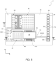
Figure 5 is a top-plan view of a possible layout of the inertial MEMS device ofFigures 4A and 4B ; -
Figure 6 is a top-plan view of a different possible layout of the inertial MEMS device ofFigure 4 ; -
Figures 7A-15A are cross-sections, similar toFigure 4A , through a semiconductor wafer in successive manufacturing steps of the inertial MEMS device ofFigure 5 ; and -
Figures 7B-15B are cross-sections, similar toFigure 4B , through the semiconductor wafer ofFigures 7A-15A , in successive manufacturing steps of the inertial MEMS device ofFigure 5 , whereinFigures 7A-15A and 7B-15B having the same figure number (7-15) relate to a same manufacturing step. - The following description refers to the arrangement shown; consequently, expressions such as "above", "below", "upper", "lower", "right", "left" relate to the accompanying figures and should not be interpreted in a limiting manner.
-
Figure 1 shows aninertial MEMS system 1 comprising aninertial MEMS device 2 and acontrol unit 3, implemented as an ASIC (Application Specific Integrated Circuit) and including control circuits for theinertial MEMS device 2. - The
inertial MEMS system 1 is for example packaged in ahousing 5 and further comprises asupply unit 6, for example a rechargeable battery, which may be enclosed in thehousing 5 or be external. - The
control unit 3 receives signals sn, typically movement signals, from theinertial MEMS device 2 and sends electrical supply and control quantities (for example a voltage P) to theinertial MEMS device 2. - The
inertial MEMS device 2 incorporates a wake-up element 10, as shown inFigure 2 . - In detail, with reference to
Figure 2 , theinertial MEMS device 2 here comprises amovable mass 9 and the wake-up element, indicated by 10 and overlying themovable mass 9. - The
inertial MEMS device 2 is electrically coupled to thecontrol unit 3, for example through firstconductive tracks 11A,first contact pads 12A andfirst wires 13A, in a per se known manner, for exchanging electrical quantities (power supply, movement signals sn). - The wake-
up element 10, as discussed in detail below, is formed here by a suspended structure, such as a membrane or cantilever, carrying a piezoelectric structure. - The piezoelectric structure is electrically coupled to the
control unit 3, for example through one or more secondconductive tracks 11B, one or moresecond contact pads 12B and one or moresecond wires 13B, and provides awakening signals, here awakening signal a1. - The wake-
up element 10, being a piezoelectric structure arranged on a membrane or cantilever, does not require power supply and is able of generating an output current if subject to shocks, accelerations or other movements; this current may be sensed and cause the activation of theinertial MEMS system 1. - In particular, activation may occur according to two activation modes, depending on the extent of the environmental change sensed, as shown in the flow diagram 20 of
Figure 3 . - In detail, in absence of environmental changes, the
inertial MEMS system 1 is in rest condition,block 22. In this condition, theinertial MEMS device 2 is off, it receives no power supply and thecontrol unit 3 operates in a minimum activity condition, with very low consumption. For example, in this condition, theinertial MEMS system 1 may consume a current of a few nA (nanoAmpere)/sec. - When the wake-
up element 10 senses a movement, an acceleration or shock, output Y fromblock 24, it generates an awakening signal a1. The awakening signal a1 (for example, a continuous signal) is provided by the wake-up element 10 to thecontrol unit 3 which verifies its amplitude. - If the awakening signal a1 is lower than a first threshold Th1, output N from
block 24, theinertial MEMS system 1 remains in the rest condition, returning toblock 22. - If the awakening signal a1 exceeds the first threshold Th1, output Y from
block 24, thecontrol unit 3 awakes theinertial MEMS system 1, comprising theinertial MEMS device 2 and its own circuits intended for powering theinertial MEMS device 2 and for processing the signals sn provided by the latter. - In particular, if the awakening signal a1 is higher than the first threshold Th1, but lower than a second threshold Th2, higher than the first threshold Th1, output N from
block 24,control unit 3 activates theinertial MEMS device 2 in low-power (low-frequency and low-consumption) mode,block 30. For example, in this condition,inertial MEMS device 2 may work with a sampling frequency of a few Hz (for example, 1.6 Hz), providing the relevant measured signal samples at such frequency. In this case, for example, theinertial MEMS system 1 may have a total consumption of the order of a few hundreds of nA (nanoAmpere)/sec. - In this working condition, the accuracy of the movement information provided by the
inertial MEMS system 1 is not high, but may be sufficient for some low-requirement applications (low-power working condition). - Furthermore, in this working condition, the
control unit 3 continues to monitor the awakening signal a1. If this remains lower than the first threshold Th1, output N fromblock 32, after some time thecontrol unit 3 stops powering theinertial MEMS device 2 and returns to the rest condition ofblock 22. - Conversely, if the awakening signal a1 is higher than the first threshold Th1, output Y from
block 32, it is verified whether the awakening signal a1 has become higher than the second threshold Th2,block 33. If not, output N fromblock 33, theinertial MEMS system 1 remains in the low-power mode, returning toblock 30. If it becomes higher, output Y fromblock 33, thecontrol unit 3 causes theinertial MEMS system 1 to work in the high-power (high-frequency, high-consumption) working mode,block 34. - Similarly, returning to
block 28, if the awakening signal a1 is higher than the second threshold Th2, output Y fromblock 28, thecontrol unit 3 activates theinertial MEMS device 2 so as to cause it to operate in high-power (high-frequency, high-consumption) mode,block 34. - For example, in the high-power mode,
block 34, theinertial MEMS device 2 may work with a sampling frequency of more than 1500Hz, providing the relative signal samples sn to thecontrol unit 3 at this frequency. In this case, for example, theinertial MEMS system 1 may have a total consumption of the order of a few tens of µA (microAmpere)/sec. - The
inertial MEMS system 1 remains in the high-power working mode (block 34) as long as the awakening signal a1 provided by the wake-up element 10 remains higher than the second threshold Th2 and/or as long as thecontrol unit 3 receives the movement signals sn (movement signals sn greater than the movement threshold). In this case, thecontrol unit 3 stops powering theinertial MEMS device 2 and takes theinertial MEMS system 1 back to the rest condition, returning to block 22. Obviously, thecontrol unit 3 may provide for more complex logics and verifications for activating the high-power operating mode, to take into account particular functions and/or specific applications. -
Figures 4A and 4B show a possible implementation of theinertial MEMS device 2 incorporating the wake-upelement 10. It should be noted that, for a better understanding of the structure and the manufacturing process,Figures 4A and 4B (as well as the followingFigures 7A-15A and 7B-15B ) show side by side two distinct zones of theinertial MEMS device 2, as indicated by the arrows A-A and B-B ofFigure 5 . - In particular,
Figures 4A and 4B refer to aninertial MEMS device 2 comprising an inertial sensor, here atriaxial accelerometer 35, of a capacitive type. - The
triaxial accelerometer 35 comprises afirst sensing portion 40, asecond sensing portion 41 and athird sensing portion 42. The sensing portions 40-42 include movable structures having a substantially planar extension, parallel to a plane XY of a Cartesian reference system XYZ. - In particular, in the embodiment of
Figures 4A and 4B , thefirst sensing portion 40 is intended for sensing oscillations along a first horizontal axis X of the Cartesian reference system XYZ; thesecond sensing portion 41 is intended for sensing oscillations along a second horizontal axis Y of the Cartesian reference system XYZ; and thethird sensing portion 42 is intended for sensing oscillations along a vertical axis Z of the Cartesian reference system XYZ. - In detail, the
inertial MEMS device 2 ofFigures 4A, 4B is formed in adie 45 of semiconductor material, comprising asubstrate 50, for example of monocrystalline silicon; an insulatinglayer 51, overlying thesubstrate 50, for example formed by a silicon oxide layer; conductive structures, for example of polycrystalline silicon, overlying the insulatinglayer 51 and formingconductive regions 52A (for example theconductive tracks Figure 2 ) and second fixed electrodes (here alower electrode 52B of thethird sensing portion 42 is visible); a firststructural layer 53, for example of polycrystalline silicon, overlying the insulatinglayer 51 and theconductive structures conductive regions 52A, or be coupled capacitively, as for thelower electrode 52B); a secondstructural layer 54, for example of polycrystalline silicon, overlying the firststructural layer 53 and mechanically and electrically coupled thereto in some zones; apiezoelectric stack 56, overlying the secondstructural layer 54; and acap 55, for example of monocrystalline silicon, overlying and attached to the secondstructural layer 54. - In the embodiment of
Figures 4A, 4B , the firststructural layer 53 has a greater thickness than the secondstructural layer 54. For example, the firststructural layer 53 may have a thickness comprised between 2 and 80 µm and the secondstructural layer 54 may have a differentiated thickness according to the zones and comprised between 1 and 2 µm. In general, the secondstructural layer 54 may have a widely variable thickness, according to the application, comprised between 0.5-1 µm and 80 µm. - Furthermore, the
inertial MEMS device 2 ofFigures 4A, 4B comprisesdielectric regions 58, arranged between the insulatinglayer 51 and the firststructural layer 53;electrical connection regions 59, for example of metal such as AlCu (aluminum-copper), arranged above the secondstructural layer 54 for forming electrical connections, for example of thecontact pads Figures 4A, 4B ; andbonding regions 68, of adhesive material, such as glassfrit, arranged between thecap 55 and the secondstructural layer 54. - In particular, the first
structural layer 53 and the secondstructural layer 54 are patterned and locally thinned so as to define movable and fixed structures of the triaxial accelerometer (movable masses, electrodes, suspension springs) and to electrically separate the various portions of thedie 45. - The
inertial MEMS device 2 has therefore structures having at least three thicknesses, and precisely structures having a first thickness, equal to the thickness of the firststructural layer 53, structures having a second thickness, equal to the sum of the thicknesses of the first and the secondstructural layers structural layer 54, due to a partial removal of the thickness of the secondstructural layer 54, as explained in detail below. - For example, in the embodiment shown in
Figures 4A, 4B , the first and thesecond sensing portions movable electrodes 60A and firstfixed electrodes 60B formed by only the firststructural layer 53 and therefore have the first thickness; thethird sensing portion 42 has the second movable mass 44 (forming second movable electrodes) formed, in the portion shown, by bothstructural layers cantilever 57 extends above the first and thesecond sensing portions structural layer 54, locally thinned, and therefore has the third thickness. - In
Figures 4A, 4B part of a suspendedmass 60C is also visible, integral with one end of thecantilever 57, formed by the first and the secondstructural layers mass 60C is here arranged laterally to thesecond sensing portion Figure 5 . - The
piezoelectric stack 56 extends on thecantilever 57 and forms, with the latter, the wake-upelement 10 ofFigure 2 . In a manner not shown, an insulating layer extends between thepiezoelectric stack 56 and thecantilever 57, electrically insulating them. - The first
fixed electrodes 60B are directly and electrically connected to respectiveconductive regions 52A through support andconnection portions 62 and face respective firstmovable electrodes 60A. - In particular, the first
movable electrodes 60A and the firstfixed electrodes 60B face each other at facing surfaces extending in the thickness direction of the first structural layer 53 (perpendicularly to the extension plane XY of the movable structures of the sensing portions 40-42). - The second
movable mass 44 overlies and capacitively coupled to thelower electrodes 52B, in a direction perpendicular to the extension plane of thetriaxial accelerometer 35. - The
cantilever 57 is suspended on the firststructural layer 53 and more precisely, in this embodiment, extends above the first and thesecond sensing portions - In particular, here, the
cantilever 57 is supported at a first end (on the right inFigure 4A ) rigid with fixed portions of thedie 45 and has a second end (on the left inFigure 4A ) integral with the suspendedmass 60C. In this manner, thecantilever 57 has a high sensitivity. - The
piezoelectric stack 56 comprises alower electrode region 63, formed by a first conductive layer (single or multiple); apiezoelectric region 64, of piezoelectric material; and anupper electrode region 65, formed by a second conductive layer (single or multiple). - For example, the
lower electrode region 63 may be formed by a platinum (Pt) layer overlying a titanium (Ti) layer, or may comprise molybdenum (Mo) and/or doped polycrystalline silicon; thepiezoelectric region 64 may be formed by a piezoelectric material such as a PZT (based on lead and titanium zirconate, Pbx[ZryTi1-y]O3), or may comprise an aluminum nitride (AlN) or scandium-doped aluminum nitride (AlScN) layer; and theupper electrode region 56 may be formed by a plurality of layers including indium tin oxide (ITO) and a tungsten-titanium (TiW) alloy or by a molybdenum (Mo) or aluminum-copper (AlCu) layer. - In particular, according to one embodiment, the
piezoelectric stack 56 may comprise an aluminum nitride layer (lower layer) and a molybdenum layer (upper layer) for the lower electrode region 63 (in which case, an insulating layer below thepiezoelectric stack 56 is not necessary); a crystalline aluminum nitride (AlN) layer for thepiezoelectric region 64; and a molybdenum layer for theupper electrode region 65. - According to a variant, the
piezoelectric region 64 may be formed by potassium sodium niobate (KNN), with lower andupper electrodes - The layers forming the
upper electrode region 64 may extend above the secondstructural layer 54, beyond thepiezoelectric stack 56, to form theconductive track 11B ofFigure 2 and be in direct electrical contact with one of theelectrical connection regions 59. - A
protection dielectric layer 66, for example of non-amorphous aluminum nitride (AlN), covers thepiezoelectric stack 56 and is open at theelectrical connection regions 59 for electrically connecting thelower electrode region 63 and theupper electrode region 65. - The
cap 55 has (in top-view) a smaller area than the first and the secondstructural layers portions 90 rigid with to the substrate 50) and by the second structural layer 54 (second fixedportions 91 overlying and rigid with the first fixed portions 90). - The
cap 55 is rigid with the second fixedportions 91 and forms, together with thesubstrate 50, the first and the second fixedportions chamber 93 enclosing the inertial sensor (triaxial accelerometer) 35 and the wake-upelement 10. - In this embodiment, the
chamber 93 is closed; in this manner, the inertial sensor (triaxial accelerometer) 35 and the wake-upelement 10 are contained in an environment closed to the outside and are protected from environmental damage, while being free to move for sensing movements of theinertial MEMS device 2. Furthermore, the wake-upelement 10 is positioned in close proximity to theinertial sensor 35, thereabove, and therefore does not require additional space and has high sensitivity. - Furthermore, since the wake-up
element 10 is positioned in close contact with the sensing portions 40-42, inside thechamber 93, it is not subject to damping due to the atmosphere. - A possible shape of the
cantilever 57 is shown inFigure 5 . - Here, the first and the
second sensing portions 40, 41 (for sensing oscillations along the first horizontal axis X and, respectively, oscillations along the second horizontal axis Y) are arranged side by side, along the first horizontal axis X, and comprise a firstmovable structure 43 integral with themovable electrodes 60A. - The third sensing portion 42 (for sensing oscillations along the vertical axis Z) is here arranged side by side with the first and the
second sensing portions movable mass 44, forming second movable electrodes. - The
cantilever 57 has here a rectangular shape and extends above the first and thesecond sensing portions - In particular, in
Figure 5 , thecantilever 57 has a length (in the direction parallel to the first horizontal axis X) approximately equal to the sum of the lengths of the first and thesecond sensing portions - Furthermore, the
cantilever 57 has a width (in the direction parallel to the second horizontal axis Y), lower than the size of the first sensing portion 40 (or of the second sensing portion 41) along the same second horizontal axis Y, even if this is not essential. - The
piezoelectric stack 56 may extend only on thefirst sensing portion 40, as shown, or may extend along theentire cantilever 57. - As an alternative to what shown, the wake-up
element 10 might be arranged only on the first or thesecond sensing portion inertial MEMS device 2 might have two wake-upelements 10, one for each sensing axis X, Y, for greater sensitivity, or one for each sensingportion element 10 might also, or only, be formed on thethird sensing portion 42. -
Figure 6 shows a different implementation of theinertial MEMS device 2. Here, theinertial MEMS device 2 comprises, in addition to the inertial sensor (triaxial accelerometer) 35, another inertial sensor, here agyroscope 36. - Here, the
gyroscope 36 is accommodated in thechamber 93 together with thetriaxial accelerometer 35 and has amovable mass 46. - Also in this embodiment, the wake-up
element 10 extends above the first and thesecond sensing portions die 45 and the suspendedmass 60C, but it might extend on only one of thesensing portions - Furthermore, if the or part of the
third sensing portion 42 and/or of thegyroscope 36 are formed only in the firststructural layer 53, the wake-upelement 10 might be (also or alternatively) formed over one or both of them, so as to have more wake-upelements 10 on two or more sensing portions 40-42 and/or on thegyroscope 36. - The
inertial MEMS device 2 is completely off in rest condition. - When the
inertial MEMS device 2 undergoes a shock or is moved, thecantilever 57, suspended, bends and/or is subject to vibrations, causing thepiezoelectric stack 56 to deform. As a result, this generates a small current, provided to thecontrol unit 3. As described above with reference toFigure 3 , when the current exceeds the first threshold Th1, thecontrol unit 3 senses it and may turn on theinertial MEMS system 1 in low- or high-power condition (depending on whether or not this current exceeds the first and the second thresholds Th1, Th2). - The
inertial MEMS device 2 ofFigures 4A, 4B may be formed as shown inFigures 7-15 and described hereinbelow. In these Figures, the layers and non-defined structures, where useful for understanding, are indicated with the same reference numerals as inFigures 4A, 4B . - In detail,
Figures 7A, 7B show asensor wafer 70 of semiconductor material comprising thesubstrate 50. - The insulating
layer 51, for example thermally grown or deposited, has been formed on thesubstrate 50. - The
conductive structures layer 51, for example by depositing a polycrystalline silicon layer and subsequent photolithographic definition. - A first
sacrificial layer 72, for example of silicon oxide, has been deposited and patterned above theconductive structures sacrificial layer 72 has been selectively removed above theconductive structures 52A, for example where the support andconnection portions 62 are to be grown as well as it is desired to grow any other anchoring and electrical and/or mechanical connection portions which connect the structures formed in the firststructural layer 53 to thesubstrate 50. - Successively,
Figures 8A, 8B , using an epitaxial growth process, the firststructural layer 53 is grown on thesensor wafer 70. The firststructural layer 53 then grows where the firstsacrificial layer 72 has been selectively removed, forming the support andconnection portions 62. - Still with reference to
Figures 8A, 8B , the firststructural layer 53 is etched, for example by dry etching, where it is desired to form the first and thesecond sensing portions first trenches 73 are formed which extend completely through the firststructural layer 53. The etching automatically stops on the firstsacrificial layer 72 and leads to the definition of the firstmovable electrodes 60A and the firstfixed electrodes 60B. - Then,
Figures 9A, 9B , a secondsacrificial layer 74, for example of TEOS (TetraEthylOrthoSilicate), is deposited for a thickness comprised, for example, between 0.1 µm and 5 µm. The secondsacrificial layer 74 may partially fill thefirst trenches 73, although such filling is not important. - The second
sacrificial layer 74 is then planarized and selectively removed. Sacrificial portions are thus formed where it is desired that the secondstructural layer 54 be separated from the firststructural layer 53 and/or have a reduced thickness. In particular, in this step a firstsacrificial region 74A, where it is desired to form thecantilever 57 ofFigures 4A, 4B , as explained below, as well as secondsacrificial regions 74B are formed. - With reference to
Figures 10A, 10B , the secondstructural layer 54 is grown above the firststructural layer 53 and the secondsacrificial layer 74. The secondstructural layer 54 is epitaxially grown and planarized, for example by CMP (Chemical Mechanical Polishing) so that, where nosacrificial regions - Subsequently,
Figures 11A, 11B , thepiezoelectric stack 56 is formed, by depositing and patterning suitable layers to form thelower electrode region 63, thepiezoelectric region 64, and theupper electrode region 65. Furthermore, theprotection dielectric layer 66 is deposited and opened where it is desired to contact theelectrode regions - Then, in a manner not shown, the
electrical connection regions 59, for example of AlCu, are formed in electrical contact with theelectrode regions 63, 65 (as regards thesecond contact pads 12B ofFigure 2 ) and with corresponding underlying portions of the first and the secondstructural layers 53, 54 (as regards thefirst contact pads 12A ofFigure 2 ). - Subsequently,
Figures 12A, 12B , thesensor wafer 70 is etched to define the structures formed by the sole secondstructural layer 54 or by bothstructural layers sensor wafer 70. In particular, here, using a mask not shown, the secondstructural layer 54 and the firststructural layer 53 are dry etched. - In detail, in this step, the second
movable mass 44 of the thirdsensitive zone 42 is defined and holes 77 are formed through the secondmovable mass 44. The secondmovable mass 44, in the part shown, therefore has the second thickness, equal to the sum of the thicknesses of the first and the secondstructural layers - Furthermore, in a manner not shown, the
cantilever 57 as well as any other structures formed only in the secondstructural layer 54 are defined, where the firststructural layer 53 is protected by thesacrificial regions - In this step, the trenches 78 (visible in
Figure 5 ) are formed and delimit the portions of the completestructural layer first contact pads 12A) and in direct electrical contact with theconductive structures conductive regions 52A. - The etching automatically stops on the first
sacrificial layer 72. - Then,
Figures 13A, 13B , the first and the secondsacrificial layers movable electrodes 60A and the secondmovable mass 44. - Furthermore, the first
movable electrodes 60A are separated from the respectivefixed electrodes 60B and the secondmovable mass 44 is separated from thelower electrode 52B. - In this step, in particular, the
sacrificial region 74A is removed, above thefirst sensing portion 40, freeing thecantilever 57. -
Figures 13A, 13B show the sensing portions 40-42 completely defined and free. - In
Figures 14A, 14B acap wafer 80 is attached to thesensor wafer 70 through thebonding regions 68, forming acomposite wafer 81. It should be noted thatFigures 14A, 14B show a wider area of thecomposite wafer 81 with respect to thesensor wafer 70 ofFigures 7A-13 , and specifically show the area of the contact pads 12 (on the right). - In these Figures, for the sake of simplicity, the first
movable electrodes 60A and the firstfixed electrodes 60B are generally indicated by 60. - The
cap wafer 80 may have previously been worked to formrecesses 82 above the sensing portions 40-42 and the wake-upelement 10, allowing ample freedom of movement thereof. - The
sensor wafer 70 may therefore be thinned, for example by CMP, so as to have a desired thickness in the direction of the vertical axis Z. - Then,
Figures 15A, 15B , thecap wafer 80 is cut, for example by laser, to open awindow 83 above the contact pads 12 (only one of thesecond contact pads 12B ofFigure 2 is visible inFigure 15A ,). - Then the
overall wafer 81 is diced to form theinertial MEMS device 2 ofFigures 4A, 4B and5 . - In this manner, the wake-up
element 10 may be easily integrated into a manufacturing process of a MEMS inertial sensor, and therefore at a very low cost, by simply modifying the masks and forming thepiezoelectric stack 56. - Furthermore, as discussed above, the wake-up
element 10 requires no additional space compared to the inertial sensor(s) integrated in theinertial MEMS device 2 and this may be used even in units and apparatuses having very small dimensions. - In addition, the wake-up
element 10 is protected from the external environment and has high sensitivity. - Finally, it is clear that modifications and variations may be made to the inertial MEMS device, the inertial MEMS system and the manufacturing process described and illustrated without thereby departing from the scope of the present invention, as defined in the attached claims.
- For example, in the flow diagram of
Figure 3 , the transition from low-power mode operation to high-power working mode (block 33) may be determined by different conditions. - An artificial intelligence algorithm may be trained to recognize the type (extent) of the movement of the inertial MEMS device and, upon sensing a fast movement (e.g. running), bring the
inertial MEMS system 1 into the high-power working mode, block 34. Conversely, if the algorithm senses a movement, but not a fast movement, it may leave theinertial MEMS system 1 in the low-power mode, returning to block 30 and enter the rest condition ofblock 22 only in absence of movement for a certain period of time (e.g. between 5 and 30 seconds), depending on the application. - Furthermore, as indicated above,
multiple cantilevers 57 may be present; the cantilevers may be arranged only on the first, the second or thethird sensing portions gyroscope 36 and the cantilever may be of projecting type, attached and integral at only one end to fixed or movable parts; or may be supported at both ends. - In practice, an inertial MEMS device (2) is disclosed, comprising:
- an inertial element (35; 36) responsive to movement, including a movable structure (43; 44; 46) formed in a first structural layer (53) of semiconductor material;
- a suspended structure (57) extending above the movable structure, at a distance therefrom, the suspended structure (57) being formed in a second structural layer of semiconductor material; and
- a piezoelectric structure (56) arranged on the suspended structure (57),
- the suspended structure (57) and the piezoelectric structure (56) forming a wake-up element (10) configured to generate an activation signal (a1) in presence of vibrations or shocks.
- A suspended mass (60C), integral to the suspended structure (57), is formed by the first and second structural layers (53, 54) and is arranged laterally to the inertial element (35; 36), so as to allow very sensitive detection of the movement of the inertial element.
- The inertial element (35; 36) includes movable electrodes (60A, 44) coupled to fixed electrodes (60B) and is connected to first connection regions (12A); the activation element (10) includes respective electrodes (63, 64) coupled to second connection regions (12B) separated from the first external connection regions.
- The inertial element (35; 36) is of a capacitive type.
- The inertial MEMS device (2) is formed in a monolithic body of semiconductor material comprising a substrate (50); the first structural layer (53) and the second structural layer (54), a cap structure (55) being attached to the second structural layer (54) and sealingly enclosing, together with the substrate, the inertial element (35; 36) and the activation element (10).
Claims (15)
- An inertial MEMS device (2), comprising:an inertial element (35; 36) responsive to movement, including a movable structure (43; 44; 46) formed in a first structural layer (53) of semiconductor material;a suspended structure (57) extending above the movable structure, at a distance therefrom, the suspended structure (57) being formed in a second structural layer of semiconductor material; anda piezoelectric structure (56) arranged on the suspended structure (57),the suspended structure (57) and the piezoelectric structure (56) forming a wake-up element (10) configured to generate an activation signal (a1) in presence of vibrations or shocks.
- The inertial MEMS device according to claim 1, wherein the suspended structure (57) is a cantilever or a membrane.
- The inertial MEMS device according to claim 1 or 2, further comprising a substrate (50) of semiconductor material, wherein the first structural layer (53) extends on the substrate and comprises first fixed portions (90) rigid with the substrate (50); the second structural layer (54) comprises second fixed portions (91) in direct contact with the first fixed portions (90); and a cap structure (55) is rigidly coupled to the second fixed portions (91) and forms, together with the substrate (50), the first fixed portions and the second fixed portions, a chamber (93) enclosing the inertial element (35; 36) and the wake-up element (10).
- The inertial MEMS device according to any of the preceding claims, wherein the first and the second structural layers (53, 53) are of silicon.
- The inertial MEMS device according to any of the preceding claims, wherein the piezoelectric structure (56) comprises a piezoelectric stack including a first electrode region (63), of a first conductive material, overlying the suspended structure (57); a piezoelectric region (64), of piezoelectric material, overlying the first electrode region (63); and a second electrode region (65), of a second conductive material, overlying the piezoelectric region (64); at least one of the first and the second electrode regions (63, 65) being coupled to external connection regions (12) .
- The inertial MEMS device according to any of the preceding claims, wherein the first structural layer (53) has a first thickness, the second structural layer (54) has a second thickness, smaller than the first thickness and the second structural layer (54) has a thin zone having a third thickness lower than the second thickness, the thin zone forming the suspended structure (57) and extending at a distance from the first structural layer (53).
- The inertial MEMS device according to any of the preceding claims, wherein the inertial element (35, 36) forms an accelerometer and/or a gyroscope.
- The inertial MEMS device according to any of the preceding claims, wherein the inertial element (35, 36) is of capacitive type.
- The inertial MEMS device according to any of the previous claims, wherein the activation element further comprises a suspended mass (60C), integral to the suspended structure (57), formed by the first and second structural layers (53, 54) and arranged laterally to the inertial element (35; 36).
- An inertial MEMS system (1) comprising an inertial MEMS device (2) according to any of the preceding claims, further comprising a control unit (3), the control unit (3) being electrically coupled to the inertial MEMS device (2) and comprising means configured to:receive the activation signal (a1);compare the activation signal (a1) with a first threshold (Th1) and a second threshold (Th2), greater than the first threshold,activate the inertial MEMS device (2) with low-consumption operation if the activation signal (a1) is greater than the first threshold and smaller than the second threshold; andactivate the inertial MEMS device (2) with high-consumption operation if the activation signal (a1) is greater than the second threshold.
- The inertial MEMS system according to the preceding claim, further comprising means configured to:
after the step of activating the inertial MEMS device (2) with low-consumption operation, receive electric measurement signals from the inertial element 35; 36; verify whether, after an acquisition time, the activation signal (a1) and/or the electric measurement signals are representative of predetermined movements; and, if the activation signal (a1) and/or the electric measurement signals are not representative of predetermined movements, deactivate the inertial MEMS device (2). - A method for activating an inertial MEMS device (2) according to any of claims 1-9, comprising:receiving the activation signal (a1);comparing the activation signal (a1) with a first threshold (Th1) and a second threshold (Th2), greater than the first threshold,activating the inertial MEMS device (2) with low-consumption operation if the activation signal (a1) is greater than the first threshold and smaller than the second threshold; andactivating the inertial MEMS device (2) with high-consumption operation if the activation signal (a1) is greater than the second threshold.
- A process for manufacturing an inertial MEMS device according to any of claims 1-9, comprising:forming a first structural layer (53) of semiconductor material on a substrate (50);forming an inertial element (35; 36), including a movable structure (43; 44; 46; 60A), in the first structural layer (53);forming a second structural layer (54) of semiconductor material on the first structural layer (53);forming a suspended structure (57) in the second structural layer (54), the suspended structure extending above the movable structure (43; 44; 46; 60A), at a distance therefrom; andforming a piezoelectric structure above the suspended structure (57),the suspended structure and the piezoelectric structure forming a wake-up element (10) configured to generate an activation signal (a1) in presence of vibrations or shocks.
- The process according to the preceding claim, wherein forming a suspended structure (57) comprises:before forming a second structural layer ((54)), forming a sacrificial region (72) above the movable structure (43; 44; 46; 60A);after the step of forming a piezoelectric structure (56), defining the second structural layer (54); and removing the sacrificial region (72).
- The process according to claim 13 or 14, further comprising attaching a cap structure (55) to the second structural layer (54) and forming, together with the substrate (50), the first structural layer (53) and the second structural layer (54), a chamber (93) enclosing the inertial element (35; 36) and the wake-up element (10).
Applications Claiming Priority (1)
| Application Number | Priority Date | Filing Date | Title |
|---|---|---|---|
| IT102023000013002A IT202300013002A1 (en) | 2023-06-23 | 2023-06-23 | INERTIAL MEMS DEVICE INTEGRATING A REACTIVATION ELEMENT, INERTIAL MEMS SYSTEM AND MANUFACTURING PROCEDURE |
Publications (2)
| Publication Number | Publication Date |
|---|---|
| EP4480899A1 true EP4480899A1 (en) | 2024-12-25 |
| EP4480899B1 EP4480899B1 (en) | 2026-02-18 |
Family
ID=87889291
Family Applications (1)
| Application Number | Title | Priority Date | Filing Date |
|---|---|---|---|
| EP24180148.9A Active EP4480899B1 (en) | 2023-06-23 | 2024-06-05 | Inertial mems device integrating a wake-up element, inertial mems system and manufacturing method |
Country Status (3)
| Country | Link |
|---|---|
| US (1) | US20240425352A1 (en) |
| EP (1) | EP4480899B1 (en) |
| IT (1) | IT202300013002A1 (en) |
Citations (2)
| Publication number | Priority date | Publication date | Assignee | Title |
|---|---|---|---|---|
| US8220330B2 (en) | 2009-03-24 | 2012-07-17 | Freescale Semiconductor, Inc. | Vertically integrated MEMS sensor device with multi-stimulus sensing |
| US20220073342A1 (en) | 2020-09-08 | 2022-03-10 | UPBEAT TECHNOLOGY Co., Ltd | Micro-electro-mechanical system acoustic sensor, micro-electro-mechanical system package structure and method for manufacturing the same |
-
2023
- 2023-06-23 IT IT102023000013002A patent/IT202300013002A1/en unknown
-
2024
- 2024-06-05 EP EP24180148.9A patent/EP4480899B1/en active Active
- 2024-06-12 US US18/741,058 patent/US20240425352A1/en active Pending
Patent Citations (2)
| Publication number | Priority date | Publication date | Assignee | Title |
|---|---|---|---|---|
| US8220330B2 (en) | 2009-03-24 | 2012-07-17 | Freescale Semiconductor, Inc. | Vertically integrated MEMS sensor device with multi-stimulus sensing |
| US20220073342A1 (en) | 2020-09-08 | 2022-03-10 | UPBEAT TECHNOLOGY Co., Ltd | Micro-electro-mechanical system acoustic sensor, micro-electro-mechanical system package structure and method for manufacturing the same |
Non-Patent Citations (2)
| Title |
|---|
| STOECKEL CHRIS ET AL.: "Wake up MEMS for inertial sensors'', 2015 IEEE International Symposium on Inertial Sensors and Systems (ISISS) Proceedings", 23 March 2015, IEEE, pages: 1 - 4 |
| STOECKEL CHRIS ET AL: "Wake up MEMS for inertial sensors", 2015 IEEE INTERNATIONAL SYMPOSIUM ON INERTIAL SENSORS AND SYSTEMS (ISISS) PROCEEDINGS, IEEE, 23 March 2015 (2015-03-23), pages 1 - 4, XP032775528, DOI: 10.1109/ISISS.2015.7102385 * |
Also Published As
| Publication number | Publication date |
|---|---|
| EP4480899B1 (en) | 2026-02-18 |
| IT202300013002A1 (en) | 2024-12-23 |
| US20240425352A1 (en) | 2024-12-26 |
Similar Documents
| Publication | Publication Date | Title |
|---|---|---|
| US12399008B2 (en) | Fused quartz dual shell resonator and method of fabrication | |
| EP0900385B1 (en) | Electrostatic drive for accelerometer | |
| JPH10508090A (en) | Dielectrically separated resonant microsensor | |
| JP2008518573A (en) | Energy recovery device with adjustable resonance frequency | |
| EP3486661B1 (en) | Microelectromechanical systems (mems) inertial sensors with energy harvesters and related methods | |
| US20120111112A1 (en) | Resonating Sensor with Mechanical Constraints | |
| EP3387381B1 (en) | Dual-sealed mems package with cavity pressure monitoring | |
| EP3608632B1 (en) | Identification of a seal failure in mems devices | |
| CN104108678A (en) | Mems Pressure Sensor, Electronic Device, Altimeter, Electronic Apparatus, And Moving Object | |
| US20150212526A1 (en) | Functional element, electronic device, electronic apparatus, and moving object | |
| US20170366107A1 (en) | Mems device for harvesting sound energy and methods for fabricating same | |
| EP4095484A1 (en) | Microelectromechanical device with out-of-plane stopper structure and process for manufacturing a microelectromechanical device | |
| US9360312B2 (en) | MEMS element, electronic device, altimeter, electronic apparatus, and moving object | |
| EP4480899B1 (en) | Inertial mems device integrating a wake-up element, inertial mems system and manufacturing method | |
| US7168321B2 (en) | Vibration-type piezoelectric acceleration sensor element and vibration-type piezoelectric acceleration sensor therewith | |
| CA3044266A1 (en) | Accelerometer sensor | |
| US5747691A (en) | Angular velocity sensor apparatus | |
| CN119178431A (en) | Inertial MEMS device integrated with wake-up element, inertial MEMS system and method of manufacture | |
| JP4367111B2 (en) | Semiconductor dynamic quantity sensor | |
| CN222784221U (en) | Piezoelectric resonant pressure sensor and pressure compensation system | |
| Laermer | Mechanical microsensors | |
| JP2006029992A (en) | Vibration type piezoelectric acceleration sensor | |
| CN117486170A (en) | MEMS sensor, thin film force-sensitive resonant element and manufacturing method thereof | |
| JP2005140516A (en) | Vibration type piezoelectric acceleration sensor element and vibration type piezoelectric acceleration sensor using the same | |
| JP2007199077A (en) | Vibration type angular velocity sensor |
Legal Events
| Date | Code | Title | Description |
|---|---|---|---|
| PUAI | Public reference made under article 153(3) epc to a published international application that has entered the european phase |
Free format text: ORIGINAL CODE: 0009012 |
|
| STAA | Information on the status of an ep patent application or granted ep patent |
Free format text: STATUS: THE APPLICATION HAS BEEN PUBLISHED |
|
| AK | Designated contracting states |
Kind code of ref document: A1 Designated state(s): AL AT BE BG CH CY CZ DE DK EE ES FI FR GB GR HR HU IE IS IT LI LT LU LV MC ME MK MT NL NO PL PT RO RS SE SI SK SM TR |
|
| STAA | Information on the status of an ep patent application or granted ep patent |
Free format text: STATUS: REQUEST FOR EXAMINATION WAS MADE |
|
| 17P | Request for examination filed |
Effective date: 20250616 |
|
| GRAP | Despatch of communication of intention to grant a patent |
Free format text: ORIGINAL CODE: EPIDOSNIGR1 |
|
| STAA | Information on the status of an ep patent application or granted ep patent |
Free format text: STATUS: GRANT OF PATENT IS INTENDED |
|
| INTG | Intention to grant announced |
Effective date: 20250919 |
|
| RIN1 | Information on inventor provided before grant (corrected) |
Inventor name: SEGHIZZI, LUCA Inventor name: VERCESI, FEDERICO Inventor name: LONGONI, GIANLUCA Inventor name: NOMELLINI, ANDREA |
|
| GRAS | Grant fee paid |
Free format text: ORIGINAL CODE: EPIDOSNIGR3 |
|
| GRAA | (expected) grant |
Free format text: ORIGINAL CODE: 0009210 |
|
| STAA | Information on the status of an ep patent application or granted ep patent |
Free format text: STATUS: THE PATENT HAS BEEN GRANTED |
|
| AK | Designated contracting states |
Kind code of ref document: B1 Designated state(s): AL AT BE BG CH CY CZ DE DK EE ES FI FR GB GR HR HU IE IS IT LI LT LU LV MC ME MK MT NL NO PL PT RO RS SE SI SK SM TR |
|
| REG | Reference to a national code |
Ref country code: CH Ref legal event code: F10 Free format text: ST27 STATUS EVENT CODE: U-0-0-F10-F00 (AS PROVIDED BY THE NATIONAL OFFICE) Effective date: 20260218 Ref country code: GB Ref legal event code: FG4D |
|
| REG | Reference to a national code |
Ref country code: DE Ref legal event code: R096 Ref document number: 602024002606 Country of ref document: DE |
|
| REG | Reference to a national code |
Ref country code: IE Ref legal event code: FG4D |