EP4480898A1 - A pressure transducer package comprising a rigid transfer block and an assembly tolerance portion - Google Patents
A pressure transducer package comprising a rigid transfer block and an assembly tolerance portion Download PDFInfo
- Publication number
- EP4480898A1 EP4480898A1 EP23180426.1A EP23180426A EP4480898A1 EP 4480898 A1 EP4480898 A1 EP 4480898A1 EP 23180426 A EP23180426 A EP 23180426A EP 4480898 A1 EP4480898 A1 EP 4480898A1
- Authority
- EP
- European Patent Office
- Prior art keywords
- package
- pressure transducer
- substrate
- transfer block
- lid
- Prior art date
- Legal status (The legal status is an assumption and is not a legal conclusion. Google has not performed a legal analysis and makes no representation as to the accuracy of the status listed.)
- Granted
Links
Images






Classifications
-
- B—PERFORMING OPERATIONS; TRANSPORTING
- B81—MICROSTRUCTURAL TECHNOLOGY
- B81B—MICROSTRUCTURAL DEVICES OR SYSTEMS, e.g. MICROMECHANICAL DEVICES
- B81B7/00—Microstructural systems ; Auxiliary parts of microstructural devices or systems
- B81B7/02—Microstructural systems ; Auxiliary parts of microstructural devices or systems containing distinct electrical or optical devices of particular relevance for their function, e.g. microelectro-mechanical systems [MEMS]
-
- B—PERFORMING OPERATIONS; TRANSPORTING
- B81—MICROSTRUCTURAL TECHNOLOGY
- B81B—MICROSTRUCTURAL DEVICES OR SYSTEMS, e.g. MICROMECHANICAL DEVICES
- B81B7/00—Microstructural systems ; Auxiliary parts of microstructural devices or systems
- B81B7/0032—Packages or encapsulation
- B81B7/0061—Packages or encapsulation suitable for fluid transfer from the MEMS out of the package or vice versa, e.g. transfer of liquid, gas, sound
-
- B—PERFORMING OPERATIONS; TRANSPORTING
- B81—MICROSTRUCTURAL TECHNOLOGY
- B81B—MICROSTRUCTURAL DEVICES OR SYSTEMS, e.g. MICROMECHANICAL DEVICES
- B81B7/00—Microstructural systems ; Auxiliary parts of microstructural devices or systems
- B81B7/0032—Packages or encapsulation
-
- B—PERFORMING OPERATIONS; TRANSPORTING
- B81—MICROSTRUCTURAL TECHNOLOGY
- B81B—MICROSTRUCTURAL DEVICES OR SYSTEMS, e.g. MICROMECHANICAL DEVICES
- B81B7/00—Microstructural systems ; Auxiliary parts of microstructural devices or systems
- B81B7/0032—Packages or encapsulation
- B81B7/007—Interconnections between the MEMS and external electrical signals
-
- B—PERFORMING OPERATIONS; TRANSPORTING
- B81—MICROSTRUCTURAL TECHNOLOGY
- B81C—PROCESSES OR APPARATUS SPECIALLY ADAPTED FOR THE MANUFACTURE OR TREATMENT OF MICROSTRUCTURAL DEVICES OR SYSTEMS
- B81C1/00—Manufacture or treatment of devices or systems in or on a substrate
- B81C1/00015—Manufacture or treatment of devices or systems in or on a substrate for manufacturing microsystems
- B81C1/00261—Processes for packaging MEMS devices
- B81C1/00309—Processes for packaging MEMS devices suitable for fluid transfer from the MEMS out of the package or vice versa, e.g. transfer of liquid, gas, sound
-
- G—PHYSICS
- G01—MEASURING; TESTING
- G01L—MEASURING FORCE, STRESS, TORQUE, WORK, MECHANICAL POWER, MECHANICAL EFFICIENCY, OR FLUID PRESSURE
- G01L19/00—Details of, or accessories for, apparatus for measuring steady or quasi-steady pressure of a fluent medium insofar as such details or accessories are not special to particular types of pressure gauges
- G01L19/0061—Electrical connection means
- G01L19/0084—Electrical connection means to the outside of the housing
-
- G—PHYSICS
- G01—MEASURING; TESTING
- G01L—MEASURING FORCE, STRESS, TORQUE, WORK, MECHANICAL POWER, MECHANICAL EFFICIENCY, OR FLUID PRESSURE
- G01L19/00—Details of, or accessories for, apparatus for measuring steady or quasi-steady pressure of a fluent medium insofar as such details or accessories are not special to particular types of pressure gauges
- G01L19/14—Housings
- G01L19/147—Details about the mounting of the sensor to support or covering means
-
- G—PHYSICS
- G01—MEASURING; TESTING
- G01L—MEASURING FORCE, STRESS, TORQUE, WORK, MECHANICAL POWER, MECHANICAL EFFICIENCY, OR FLUID PRESSURE
- G01L19/00—Details of, or accessories for, apparatus for measuring steady or quasi-steady pressure of a fluent medium insofar as such details or accessories are not special to particular types of pressure gauges
- G01L19/14—Housings
- G01L19/148—Details about the circuit board integration, e.g. integrated with the diaphragm surface or encapsulation
-
- H—ELECTRICITY
- H04—ELECTRIC COMMUNICATION TECHNIQUE
- H04R—LOUDSPEAKERS, MICROPHONES, GRAMOPHONE PICK-UPS OR LIKE ACOUSTIC ELECTROMECHANICAL TRANSDUCERS; ELECTRIC HEARING AIDS; PUBLIC ADDRESS SYSTEMS
- H04R19/00—Electrostatic transducers
-
- H—ELECTRICITY
- H04—ELECTRIC COMMUNICATION TECHNIQUE
- H04R—LOUDSPEAKERS, MICROPHONES, GRAMOPHONE PICK-UPS OR LIKE ACOUSTIC ELECTROMECHANICAL TRANSDUCERS; ELECTRIC HEARING AIDS; PUBLIC ADDRESS SYSTEMS
- H04R19/00—Electrostatic transducers
- H04R19/005—Electrostatic transducers using semiconductor materials
-
- H—ELECTRICITY
- H04—ELECTRIC COMMUNICATION TECHNIQUE
- H04R—LOUDSPEAKERS, MICROPHONES, GRAMOPHONE PICK-UPS OR LIKE ACOUSTIC ELECTROMECHANICAL TRANSDUCERS; ELECTRIC HEARING AIDS; PUBLIC ADDRESS SYSTEMS
- H04R19/00—Electrostatic transducers
- H04R19/04—Microphones
-
- B—PERFORMING OPERATIONS; TRANSPORTING
- B81—MICROSTRUCTURAL TECHNOLOGY
- B81B—MICROSTRUCTURAL DEVICES OR SYSTEMS, e.g. MICROMECHANICAL DEVICES
- B81B2201/00—Specific applications of microelectromechanical systems
- B81B2201/02—Sensors
- B81B2201/0257—Microphones or microspeakers
-
- B—PERFORMING OPERATIONS; TRANSPORTING
- B81—MICROSTRUCTURAL TECHNOLOGY
- B81B—MICROSTRUCTURAL DEVICES OR SYSTEMS, e.g. MICROMECHANICAL DEVICES
- B81B2201/00—Specific applications of microelectromechanical systems
- B81B2201/02—Sensors
- B81B2201/0264—Pressure sensors
-
- B—PERFORMING OPERATIONS; TRANSPORTING
- B81—MICROSTRUCTURAL TECHNOLOGY
- B81B—MICROSTRUCTURAL DEVICES OR SYSTEMS, e.g. MICROMECHANICAL DEVICES
- B81B2203/00—Basic microelectromechanical structures
- B81B2203/01—Suspended structures, i.e. structures allowing a movement
- B81B2203/0127—Diaphragms, i.e. structures separating two media that can control the passage from one medium to another; Membranes, i.e. diaphragms with filtering function
-
- B—PERFORMING OPERATIONS; TRANSPORTING
- B81—MICROSTRUCTURAL TECHNOLOGY
- B81B—MICROSTRUCTURAL DEVICES OR SYSTEMS, e.g. MICROMECHANICAL DEVICES
- B81B2207/00—Microstructural systems or auxiliary parts thereof
- B81B2207/01—Microstructural systems or auxiliary parts thereof comprising a micromechanical device connected to control or processing electronics, i.e. Smart-MEMS
- B81B2207/012—Microstructural systems or auxiliary parts thereof comprising a micromechanical device connected to control or processing electronics, i.e. Smart-MEMS the micromechanical device and the control or processing electronics being separate parts in the same package
-
- B—PERFORMING OPERATIONS; TRANSPORTING
- B81—MICROSTRUCTURAL TECHNOLOGY
- B81B—MICROSTRUCTURAL DEVICES OR SYSTEMS, e.g. MICROMECHANICAL DEVICES
- B81B2207/00—Microstructural systems or auxiliary parts thereof
- B81B2207/07—Interconnects
-
- H—ELECTRICITY
- H04—ELECTRIC COMMUNICATION TECHNIQUE
- H04R—LOUDSPEAKERS, MICROPHONES, GRAMOPHONE PICK-UPS OR LIKE ACOUSTIC ELECTROMECHANICAL TRANSDUCERS; ELECTRIC HEARING AIDS; PUBLIC ADDRESS SYSTEMS
- H04R1/00—Details of transducers, loudspeakers or microphones
- H04R1/02—Casings; Cabinets ; Supports therefor; Mountings therein
- H04R1/04—Structural association of microphone with electric circuitry therefor
-
- H—ELECTRICITY
- H04—ELECTRIC COMMUNICATION TECHNIQUE
- H04R—LOUDSPEAKERS, MICROPHONES, GRAMOPHONE PICK-UPS OR LIKE ACOUSTIC ELECTROMECHANICAL TRANSDUCERS; ELECTRIC HEARING AIDS; PUBLIC ADDRESS SYSTEMS
- H04R19/00—Electrostatic transducers
- H04R19/02—Loudspeakers
-
- H—ELECTRICITY
- H04—ELECTRIC COMMUNICATION TECHNIQUE
- H04R—LOUDSPEAKERS, MICROPHONES, GRAMOPHONE PICK-UPS OR LIKE ACOUSTIC ELECTROMECHANICAL TRANSDUCERS; ELECTRIC HEARING AIDS; PUBLIC ADDRESS SYSTEMS
- H04R2201/00—Details of transducers, loudspeakers or microphones covered by H04R1/00 but not provided for in any of its subgroups
- H04R2201/003—Mems transducers or their use
Definitions
- Embodiments of the present disclosure relate to housed electronic components, and in particular to microstructured MEMS (Micro Electro Mechanical System) pressure transducers, such as environmental pressure sensors. Impinging sound waves may also be detected by pressure transducers, in which case they may be referred to as sound transducers, such as microphones or speakers.
- MEMS Micro Electro Mechanical System
- MEMS pressure transducers and in particular MEMS sound transducers, are an integral part of nowadays consumer electronics.
- smartphones, tablets, smart watches, and the like are usually equipped with one or more sound transducers, such as microphones and speakers.
- these consumer devices comprise an ever increasing amount of integrated electronic components in order to satisfy the consumers needs and desires for increasing features.
- the size and form factor of the devices tends to decrease.
- assembly space inside a casing of an electronic device may be highly limited, such that manufacturers of integrated electronic components need to find new solutions for installing their components into small-sized devices.
- One of the challenging tasks is to properly fit MEMS pressure transducers, including microphones and speakers, into a casing of a consumer electronics device, since these MEMS components need ad-ditionall space for fluid channels for communicating with the environment.
- microphones and speakers need sound ports and sound channels for receiving and transmitting sound waves from an external environment surrounding the casing.
- these kind of MEMS devices may additionally comprise a predetermined mounting direction that has to be considered.
- MEMS devices are usually housed in packages, wherein said packages do also have to comprise fluid openings for allowing a fluid communication of the MEMS with the surrounding environment.
- MEMS pressure transducers are to be mounted such that they cover the respective fluid opening of the package. Thereby, the MEMS pressure transducer may use the entire volume of the package as a back volume.
- MEMS devices may be connected to package pads by means of flexible bond wires, i.e. the above mentioned gap can be bridged by a bond wire.
- the flexibility of the bond wire is preferred since it may account for assembly misalignments, for example if the MEMS device is not exactly positioned at its actual mounting position.
- the flexible bond wire may be connected to the MEMS by means of soldering.
- stiff and rigid connection means have to be used for providing a physical and electrical contact between the MEMS and the package pads when the package is closed.
- the stiff connection means provide a mechanical and electrical contact, comparable to a plug and socket connection.
- the MEMS has to be placed very precisely (preferably without any assembly tolerances) at its intended mounting position. Even smallest assembly tolerances, which are not completely avoidable in real life, may cause a statically overdefined indeterminate mechanical system leading to undesired faults and breakages of the stiff connection means.
- a MEMS pressure transducer package having an electric connection that reliably bridges a physical gap between a MEMS and a package pad enclosed inside a closed package housing, and which, at the same time, allows for assembly tolerances of the MEMS relative to the package pad inside the closed housing.
- the pressure transducer package comprises a substrate and a lid being attached to the substrate, wherein a cavity is defined underneath the lid, and a MEMS pressure transducer arranged inside the cavity.
- the package further comprises a fluid port for allowing a fluid communication between an interior and an exterior of the cavity, wherein the MEMS pressure transducer is mounted such that it covers said fluid port.
- the package further comprises a conductive package pad for electrically contacting the MEMS pressure transducer from outside the package. The package pad is provided at a first side of the package, while the fluid port is provided at an opposite second side of the package.
- the package further comprises a rigid transfer block arranged inside the cavity, the transfer block being configured to provide an electric path between the MEMS pressure transducer and the oppositely arranged package pad.
- at least one of the lid and the rigid transfer block comprises an assembly tolerance portion for providing a mechanical assembly tolerance between the rigid transfer block and at least one of the substrate and the lid.
- Method steps which are depicted by means of a block diagram and which are described with reference to said block diagram may also be executed in an order different from the depicted and/or described order. Furthermore, method steps concerning a particular feature of a device may be replaceable with said feature of said device, and the other way around.
- MEMS sound transducers and in particular MEMS microphones, may be described as non-limiting examples for MEMS pressure transducers in general.
- each embodiment described herein may comprise a general pressure transducer, such as an environmental pressure sensor or the like.
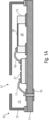
- Figure 1A shows a MEMS microphone package 10 in a standard top-port configuration.
- the package 10 comprises a substrate 11.
- a lid 12 is attached to the substrate 11, such that a cavity 13 is formed between the lid 12 and the substrate 11.
- the lid 12 comprises an opening 14 through which the cavity 13 is in fluid communication with a package-external environment, i.e. the opening 14 allows for a fluid exchange between an interior and an exterior of the cavity 13.
- the opening 14 may also be referred to as a fluid port.
- the opening 14 may also be referred to as a sound port.
- a MEMS microphone 15 is arranged inside the cavity 13.
- the MEMS microphone 15 may be attached to the substrate 11.
- the package 10 comprises a conductive package pad 16 for electrically contacting the MEMS microphone 15 from outside the package 10.
- Electric conductors such as bond wires 17, 18, may provide an electric path between the package pad 16 and the MEMS microphone 15.
- a controlling circuitry 21 may sit between the package pad 16 and the MEMS microphone 15 in said electric path.
- sound waves may enter the cavity 13 through the sound port 14 provided in the lid 12.
- the sound waves may impinge on the microphone membrane 19 of the MEMS microphone 15, in response to which the microphone membrane 19 oscillates.
- These oscillations create a corresponding electric signal that can be conducted through the electric conductors 17, 18, via the optionally available circuitry 21, to the package pad 16, from which the signal can be picked up from outside the package 10.
- a free space underneath the microphone membrane 19, i.e. between the microphone membrane 19 and the substrate 11, may be referred to as a so-called back volume 20.
- SNR signal-to-noise ratio
- the size of the back volume 20 is limited by the size of the free space underneath the microphone membrane 19.
- Figure 1B shows an alternative solution for providing a larger back volume 20.
- This exemplary configuration may be referred to as a so-called bottom-port configuration.
- the sound port 14 is not provided in the lid 12, but in the substrate 11 instead. More particular, the substrate 11 comprises the sound port 14 which enables a fluid exchange between the interior and the exterior of the cavity 13.
- the MEMS microphone 15 covers the sound port 14.
- the bottom-port configuration of Figure 1B provides a much larger back volume 20.
- the entire cavity 13 can be used as the back volume 20.
- the MEMS microphone 15 in the bottom-port configuration may comprise a better sensitivity and lower SNR than in the aforementioned top-port configuration.
- Figure 1C shows a flipped top-port configuration, in which the package pad 16 may be provided on the substrate 11, while the MEMS microphone 15 may be attached to the lid 12 for covering the sound port 14 formed therein.
- the substrate 11 cannot be completely pre-assembled during the package assembly process, i.e. before the lid 12 is attached.
- the package 10 is closed such that the interior 13 of the package 10 cannot be accessed anymore. Accordingly, there is no possibility to provide flexible bond wires for connecting the MEMS microphone 15 (lid-side) with the opposite package pad 16 (substrate-side) since it is not possible anymore to access the interior 13 of the closed package 10.
- the MEMS microphone 15 has to be placed very precisely (preferably without any assembly tolerances) at its intended mounting position. Even smallest assembly tolerances, which are not avoidable in real life, may cause a statically overdefined indeterminate mechanical system leading to undesired faults and breakages of the stiff connection means.
- the distance d between the lid 12 and the substrate 11 is dictated by the height h of the lid 12 and the thickness t of the applied mounting means 22 (e.g., adhesives, solder, etc.).
- stiff and rigid connection means were applied between the MEMS microphone 15 and the package pad 16, they would have to have an extremely precise shape and length in order to exactly fit the distance d. Otherwise, they would either be too short thereby failing to provide a proper electric connection, or they would be too large causing an obstruction such that the lid 12 cannot be properly closed. Both cases describe a statically overdefined indeterminate mechanical system.
- a MEMS pressure transducer 150 is arranged inside the cavity 130.
- the MEMS pressure transducer 150 may be configured as a MEMS sound transducer, and in particular as a MEMS microphone.
- the MEMS pressure transducer 150 may also be configured as a MEMS speaker, a MEMS ambient pressure sensor, or any other kind of MEMS pressure transducer.
- the package 100 further comprises a fluid port 140 for allowing a fluid exchange between an interior and an exterior of the cavity 130, wherein the MEMS pressure transducer 150 is mounted such that it covers said fluid port 140.
- the fluid port 140 is provided in the lid 120.
- the fluid port 140 may be provided in the substrate 110, examples of which may be described somewhat later in this description.
- the MEMS pressure transducer 150 is configured as a sound transducer
- the fluid port 140 may also be referred to as a sound port.
- the package 100 further comprises a conductive package pad 160 for electrically contacting the MEMS pressure transducer 150 from outside the package 100.
- the package pad 160 and the fluid port 140 are positioned on two opposite sides 101, 102 of the package 100, i.e. the package pad 160 may be provided at a first side 101 of the package 100, while the fluid port 140 may be provided at an opposite second side 102 of the package 100.
- the fluid port 140 may be provided in (or at) at least one of the lid 120 and the substrate 110, while the package pad 160 may be provided in (or at) the other one of the lid 120 and the substrate 110.
- the fluid port 140 is provided in the lid 120, while the package pad 160 is provided in the substrate 110.
- the MEMS pressure transducer 150 is mounted directly at the fluid port 140, i.e. such that it covers the fluid port 140, the MEMS pressure transducer 150 and the package pad 160 may also be positioned on two opposite sides 101, 102 of the package 100. Nevertheless, the MEMS pressure transducer 150 has to be electrically connected somehow to the oppositely arranged package pad 160.
- the package 100 is closed, while inside the closed package 100 a physical gap remains between the MEMS pressure transducer 150 on the one package side 101 and the package pad 160 on the opposite other package side 102. As mentioned above, this gap needs to be bridged somehow with an electric conductor for electrically connecting the MEMS pressure transducer 150 with the oppositely positioned package pad 160. However, since the package 100 is closed it is not accessible anymore and, thus, it is not possible to subsequently provide flexible electric conductors (e.g., bond wires, etc.) inside the closed package 100 for connecting the MEMS pressure transducer 150 with the package pad 160.
- flexible electric conductors e.g., bond wires, etc.
- the innovative package 100 comprises a rigid transfer block 180 that is arranged inside the cavity 130, the rigid transfer block 180 being configured to provide an electric path between the MEMS pressure transducer 150 and the oppositely arranged package pad 160.
- the rigid transfer block 180 is configured to provide an assembly tolerance between the MEMS pressure transducer 150 and the package pad 160 upon assembly of the package 100, such that the lid 120 (including the MEMS pressure transducer 150) can be mounted and attached to the substrate 110 with a certain assembly tolerance. Therefore, according to an embodiment, the rigid transfer block 180 comprises an assembly tolerance portion 170.
- the assembly tolerance portion 170 provides a mechanical assembly tolerance between the rigid transfer block 180 and the substrate 110, and/or between the rigid transfer block 180 and the lid 120.
- the lid 120 may comprise an assembly tolerance portion 170.
- the assembly tolerance portion 170 may provide a mechanical assembly tolerance between the rigid transfer block 180 and the lid 120, examples and embodiments of which will be described somewhat later.
- the assembly tolerance portion 170 provides a mechanical assembly tolerance
- the assembly tolerance portion 170 allows for a relative displacement / misalignment between the lid 120 (including any components arranged thereon) and the substrate 110 (including any components arranged thereon) during assembly of the package 100, while still properly establishing an electric path between the MEMS pressure transducer 150 and the oppositely arranged package pad 160.
- the electric path between the MEMS pressure transducer 150 and the oppositely arranged package pad 160 may still be properly established even if the lid 120 was attached to the substrate 110 with some misalignment. This is due to the fact that some predetermined assembly tolerance may be provided by the assembly tolerance portion 170.
- flexible connectors would provide a statically underdefined indeterminate mechanical system, which is desirable for opposite-port-pad configurations since it allows for some assembly tolerance or misalignment. However, they cannot be subsequently installed.
- Rigid connectors instead, may be easy to install but would provide a statically overdefined indeterminate mechanical system.
- the herein described innovative concept combines the advantages of both connecting principles. Even though the transfer block 180 is rigid, the innovative assembly tolerance portion 170 allows for some displacement/ misalignment between the lid 120 and the substrate 110. In other words, even though the transfer block 180 is rigid, the additional assembly tolerance portion 170 provides for a statically underdefined indeterminate mechanical system. This explanation refers to a static mechanical system, in which the lid 120, the rigid transfer block 180 and the substrate 110 are mechanically connected to each other.
- the assembly tolerance portion 170 even allows for some misalignment of the rigid transfer block 180 itself.
- the rigid transfer block 180 may be mounted between the substrate 110 and the lid 120.
- the rigid transfer block 180 may be fixedly attached to at least one (or exactly one) of the substrate 110 and the lid 120.
- the transfer block 180 may be fixedly attached (e.g., by means of glue) to the inside of the lid 120.
- the rigid transfer block 180 may be fixedly attached to the substrate 110.
- the position at which the transfer block 180 is fixedly mounted / attached is referred to as its predetermined mounting position.
- the assembly tolerance portion 170 allows to keep the rigid transfer block 180 at its predetermined mounting position, even if the lid 120 and the substrate 110 were misaligned during assembly.
- an electric path may be provided inside the package 100 between the MEMS pressure transducer 150 and the oppositely arranged package pad 160.
- the transfer block 180 may be configured to provide the electric path between the MEMS pressure transducer 150 and the oppositely arranged package pad 160. Therefore, the transfer block 180 may be electrically connected to the MEMS pressure transducer 150 and the package pad 160, e.g., by means of rigid or flexible connectors, such as wire bonds 121.
- a wire bond connection 121 between the MEMS pressure transducer 150 and the rigid transfer block 180 may be easily provided since both are arranged on the same package-side, e.g. at the lid 120, such that a pre-assembly is possible before finally closing the package 100.
- the transfer block 180 may be mounted directly adjacent to the MEMS pressure transducer 150, without any further components in between.
- a short length of the conductive connector 121 may enhance the RF stability, since a short conductive connector 121 is less prone to RF interference.
- a first conductive path may be provided between the rigid transfer block 180 and the MEMS pressure transducer 150
- a second conductive path may be provided between the rigid transfer block 180 and the package pad 160.
- the first and second conductive paths may be parts of the electric path between the MEMS pressure transducer 150 and the package pad 160.
- a controlling circuitry 190 for controlling the MEMS pressure transducer 150 may be arranged inside the package 100, wherein the controlling circuitry 190 may sit in the electric path between the MEMS pressure transducer 150 and the package pad 160.
- the controlling circuitry 190 may be coupled to the electric path by means of electric conductors, such as wire bonds, as exemplarily depicted in Figure 2 , or via flip-chip bonding.
- controlling circuitry 190 is optional since it may also be arranged outside the package 100, where it would not sit in the electric path between the MEMS pressure transducer 150 and the package pad 160. Accordingly, even though it is exemplarily depicted in Figure 2 that the rigid transfer block 180 may be coupled to an internal controlling circuitry 190, the rigid transfer block 180 may be directly coupled to the package pad 160.
- any electric connections on the substrate 110 may be provided by means of a conductive wiring provided in or at the substrate 110.
- Said wiring may comprise at least one of conducting wire bonds 122, conducting surface pads 123, conducting surface traces (not shown) and conducting layers 124 integrated into the substrate 110.
- the substrate 110 may be a Printed Circuit Board (PCB).
- the transfer block 180 may comprise at least one of the above mentioned electric conductors.
- the transfer block 180 may be made of, or may comprise, a material similar to a Printed Circuit Board (PCB), such as resin, wherein one or more electric conductors 125 may be implemented in one or more layers of the transfer block 180.
- the rigid transfer block 180 may comprise at least one of conductive surface pads 126 and conductive surface traces 125.
- the rigid transfer block 180 is firmly attached to the lid 120 and spaced apart from the substrate 110, wherein a physical gap remains between the rigid transfer block 180 and the substrate 110.
- the assembly tolerance portion 170 may comprise a conductive pin 171 for bridging the gap and for providing a conductive path between the rigid transfer block 180 and the substrate 110.
- the assembly tolerance portion 170 may further comprise a recess 172 provided in the rigid transfer block 180, wherein the conductive pin 171 is, at least partly, arranged inside said recess 172.
- the recess 172 may be wider than a width of the conductive pin 171, such that the conductive pin 171 is accommodated inside the recess 172 by a clearance-fit.
- the pin 171 can move inside the recess 172 in a clearance-fit manner, thereby providing an assembly tolerance that allows for a misalignment of the lid 120 relative to the substrate 110.
- a recess 173 may be provided in the substrate 110.
- the recesses 172, 173 may be positioned opposite to each other.
- the conductive pin 171 may be, at least partly, arranged inside said recess 173 in the substrate 110.
- the recess 173 in the substrate 110 may be wider than a width of the conductive pin 171, such that the conductive pin 171 is accommodated inside the recess 173 by a clearance-fit.
- the pin 171 can move inside the recess 173 in a clearance-fit manner, thereby providing an assembly tolerance that allows for a misalignment of the lid 120 relative to the substrate 110.
- a clearance between the conductive pin 171 and the recess 172, and/or a clearance between the conductive pin 171 and the recess 173, may be filled with conductive filler material, for example solder, solder paste, or a conductive adhesive.
- a conductive adhesive may comprise an anisotropically conductive adhesive material (ACA) or an anisotropically conductive film material (ACF).
- ACA anisotropically conductive adhesive material
- ACF anisotropically conductive film material
- the recesses 172, 173 may serve the purpose of a reservoir, e.g. a solder reservoir or a glue reservoir, that may be partly or completely filled with the respective conductive filler material.
- the conductive filler material may be elastic, at least prior to or during assembly of the package 100.
- the conductive filling material may comprise an adhesive that is elastic, at least prior to curing.
- the filling material may be applied to the recess 172, 173 during a pre-assembly step, i.e. prior to attaching the lid 120 to the substrate 110.
- the filling material may be liquid, pasty or viscous.
- the filler material may cure, wherein the filler material may remain elastic or may become inelastic at room temperature.
- an adhesive may be permanently elastic at room temperature even after curing, or it may be temporarily elastic at room temperature such that it becomes stiff and inelastic after curing.
- the bonding material 250 may comprise a permanently elastic soft glue.
- Figure 4 shows a further embodiment of the package 100, wherein like elements with like or similar functionality as in Figures 2 and 3 are denoted with like reference numerals.
- the MEMS pressure transducer 150 covering the fluid port 140 may be arranged at or on the lid 120, while the package pad 160 may be arranged at or on the substrate 110.
- the MEMS pressure transducer 150 and the package pad 160 are arranged on two opposite sides of the package 100.
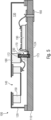
- FIG. 5 shows a further embodiment of the package 100, wherein like elements with like or similar functionality as in the previous Figures are denoted with like reference numerals.
- the MEMS pressure transducer 150 covering the fluid port 140 may be arranged at or on the lid 120, while the package pad 160 may be arranged at or on the substrate 110.
- the MEMS pressure transducer 150 and the package pad 160 are arranged on two opposite sides of the package 100.
- the conductive pin 171 may either comprise a bent portion 174, as depicted in Figure 3 , or the conductive pin 171 may be formed as a straight and rigid pin, as depicted in Figure 2 .
- a difference compared to the previously discussed embodiments is the additional insulation structure 230 provided at the outer circumference of the conductive pin 171.
- the insulation structure 230 may protect the conductive pin 171 from shorting.
- FIG. 6 shows a further embodiment of the package 100, wherein like elements with like or similar functionality as in the previous Figures are denoted with like reference numerals.
- the MEMS pressure transducer 150 covering the fluid port 140 may be arranged at or on the lid 120, while the package pad 160 may be arranged at or on the substrate 110.
- the MEMS pressure transducer 150 and the package pad 160 are arranged on two opposite sides of the package 100.
- the rigid transfer block 180 may be configured as one integral part extending gaplessly between the lid 120 and the substrate 110, i.e. there is no physical gap remaining between the transfer block 180 and the substrate 110.
- the MEMS pressure transducer 150 is mounted on the lid 120 such that it covers the fluid port 140 provided in the lid 120.
- the package pad 160 is provided at the substrate 110 and, thus, arranged on an opposite side of the MEMS pressure transducer 150.
- the rigid transfer block 180 may comprise an assembly tolerance portion 170.
- the assembly tolerance portion 170 may comprise an accommodating portion 175 being provided at the rigid transfer block 180, wherein said accommodating portion 175 may be accommodated in a hole 128 provided in the lid 120.
- the accommodating portion 175 may be provided as a protruding portion that protrudes from a surface of the transfer block 180.
- the accommodating portion 175 may be provided at an upper surface of the transfer block 180 that faces the lid 120.
- the accommodating portion 175 may be inserted into the hole 128 in the lid 120.
- the accommodating portion 175 may be flush with the outer surface of the lid 120.
- the rigid transfer block 180 may comprise an accommodating portion being provided at a lower surface of the transfer block 180 that faces the substrate 110. This accommodating portion may be accommodated in a hole provided in the substrate 110. The accommodating portion 175 may be inserted into the hole in the substrate 110.
- the hole 128 in the lid 120 and/or in the substrate 110 may be wider than a width of the accommodating portion 175, such that the accommodating portion 175 is accommodated inside the hole 128 by a clearance-fit.
- the accommodating portion 175 of the transfer block 180 may comprise a width that may be 1.2 times to 1.8 times smaller than the width of the hole 128.
- the hole 128 in the lid 120 may comprise a width between 0.7 mm and 0.8 mm, while the accommodating portion 175 may comprise a width between 0.4 mm and 0.6 mm.
- a clearance between the accommodating portion 175 and the hole 128 in the lid 120 may be between 0.1 mm and 0.4 mm.
- a clearance between the accommodating portion 175 and the hole 128 may be filled with bonding material 250, in particular with non-conductive bonding material, such as glue.
- the non-conductive bonding material 250 may be permanently elastic, such that it is elastic prior to and after curing.
- the bonding material 250 may comprise a permanently elastic soft glue.
- the non-conductive bonding material 250 may be temporarily elastic, such that it is elastic prior to curing but non-elastic after curing.
- the accommodating portion 175 bearing the bonding material 250 may be loosely inserted into the hole 128. Accordingly, also the rigid transfer block 180 would then be loosely attached to the lid 120.
- the rigid transfer block 180 can be electrically coupled, e.g. by means of bond wires 121, to the MEMS pressure transducer 150 that may be fixedly secured to the lid 120.
- the transfer block 180 can be fixedly secured to the lid 120, e.g. by curing the non-conductive bonding material 250.
- the rigid transfer block 180 may then be electrically coupled, and fixedly secured, to the substrate 110 by means of solder 240 using a thermal reflow process.
- the rigid transfer block 180 may be attached to, and fixedly secured, to the substrate 110 in a pre-assembly step, e.g. by means of solder or glue 240.
- the lid 120 can be attached to the substrate 110 such that the hole 128 in the lid 120 is positioned opposite to the accommodating portion 175 of the rigid transfer block 180.
- the hole 128 in the lid 120 can be put over the accommodating portion 175 bearing the bonding material 250.
- the clearance-fit between the accommodating portion 175 and the hole 128 provides a mechanical assembly tolerance, such that the lid 120 can be attached to the substrate 110 with some misalignment.
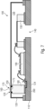
- FIG. 7 shows a further embodiment of the package 100, wherein like elements with like or similar functionality as in the previous Figures are denoted with like reference numerals.
- the MEMS pressure transducer 150 covering the fluid port 140 may be arranged at or on the substrate 110, while the package pad 160 may be arranged at or on the rigid transfer block 180, in particular at a surface of the transfer block 180 facing away from the substrate 110.
- the MEMS pressure transducer 150 and the package pad 160 are arranged on two opposite sides of the package 100.
- the fluid port 140 is provided in the substrate 110, e.g. formed as a through hole extending between two opposite surfaces of the substrate 110.
- the MEMS pressure transducer 150 is mounted on the substrate 110 such that it covers the fluid port 140.
- the rigid transfer block 180 may be configured as one integral part extending gaplessly between the lid 120 and the substrate 110, i.e. there is no physical gap remaining between the transfer block 180 and the substrate 110.
- the assembly tolerance portion 170 may comprise an accommodating portion 175 being provided at the rigid transfer block 180, wherein said accommodating portion 175 may be accommodated in a hole 128 provided in the lid 120.
- said rigid transfer block 180, the accommodating portion 175, the hole 128 and the bonding material 250 it is to be noted that everything that was mentioned before, with reference to Figure 6 , correspondingly applies to the embodiment of Figure 7 .
- the package pad 160 may be arranged at the rigid transfer block 180, and in particular at the accommodating portion 175 accommodated inside the hole 128 in the lid 120.
- the package pad 160 may protrude from the hole 128 in the lid 120 for being externally contactable from outside the package 100.
- the rigid transfer block 180 may be electrically and mechanically coupled to the substrate 110 by means of a bonding means 260, such as solder or glue.
- a bonding means 260 such as solder or glue.
- the rigid transfer block 180 may be coupled to a surface pad 260 provided at a surface of the substrate 110.
- An integrated conducting layer 124 may electrically connect the surface pad 260 with the MEMS pressure transducer 150, wherein the aforementioned integrated circuitry 190 may optionally sit in between.
- conducting surface pads, conducting surface traces and integrated conducting layers may be part of the wiring of the substrate 110. Accordingly, stated in more general terms, the rigid transfer block 180 may be conductively coupled to a wiring being provided in or at the substrate 110 for establishing the electric path between the package pad 160 and the oppositely arranged MEMS pressure transducer 150.
- FIG 8 shows a further embodiment of the package 100, wherein like elements with like or similar functionality as in the previous Figures are denoted with like reference numerals.
- the MEMS pressure transducer 150 covering the fluid port 140 may be arranged at or on the substrate 110, while the package pad 160 may be arranged at or on the rigid transfer block 180, in particular at a surface of the transfer block 180 facing away from the substrate 110.
- the MEMS pressure transducer 150 and the package pad 160 are arranged on two opposite sides of the package 100.
- the rigid transfer block 180 may comprise a conductive connection pad 270 for establishing the electric path between the package pad 160 and the MEMS pressure transducer 150, wherein the conductive connection pad 270 is spatially and galvanically separated from the substrate 110.
- the rigid transfer block 180 may comprise a protruding portion 181 at which the conductive connection pad 270 may be arranged.
- the protruding portion 181 may laterally protrude from the contour of the rigid transfer block 180.
- the conductive connection pad 270 may be arranged at said protruding portion 181 such that the protruding portion 181 is positioned between the conductive connection pad 270 and the substrate 110.
- the electric path between the package pad 160 and the oppositely arranged MEMS pressure transducer 150 may be established by electric connectors 121, such as bond wires, for example.
- the electric connectors 121 may be connected to the conductive connection pad 270.
- the conductive connection pad 270 and the package pad 160 may be electrically coupled to each other by means of wirings provided in or at the rigid transfer block 180. Accordingly, by connecting the MEMS pressure transducer 150 to the conductive connection pad 270, the MEMS pressure transducer 150 is also coupled to the package pad 160.
- a controlling circuitry 190 may sit in the electric path between the MEMS pressure transducer 150 and the package pad 160.
- the substrate 110 may be configured as a wiring-less substrate, i.e. the substrate 110 does not need to be equipped with expensive wirings, such as surface pads, surface traces or integrated conductive layers.
- expensive wirings such as surface pads, surface traces or integrated conductive layers.
- a simple plastics substrate may be sufficient in this case.
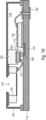
- Figure 9 shows a further embodiment of the package 100, wherein like elements with like or similar functionality as in the previous Figures are denoted with like reference numerals.
- the MEMS pressure transducer 150 covering the fluid port 140 may be arranged at or on the lid 120, while the package pad 160 may be arranged at or on the substrate 110.
- the MEMS pressure transducer 150 and the package pad 160 are arranged on two opposite sides of the package 100.
- the rigid transfer block 180 may be similar to the embodiments discussed with reference to Figure 6 . However the embodiment of Figure 8 can be combined with each embodiment in which the rigid transfer block 180 is coupled to the lid 120.
- the lid 120 comprises one or more flexible tongues 221, 222.
- the flexible tongues 221, 222 may be integrally formed with the lid 120.
- the one or more flexible tongues 221, 222 may be created by providing some cutout portions in the lid 120, and by bending the remaining lid material portions to the inside, i.e. in the direction of the cavity 130.
- the transfer block 180 may comprise a conductive connection pad 260 via which it is conductively coupled to the solder connector 280.
- the solder connector 280 may be conductively coupled with the substrate 110 by means of the wiring of the substrate 110, e.g. by means of a conductive surface pad, or the like.
- the bonding material 250 may be permanently elastic, such that it is elastic prior to and after curing.
- the bonding material 250 may comprise a permanently elastic soft glue.
- the non-conductive bonding material 250 may be temporarily elastic, such that it is elastic prior to curing but non-elastic after curing.
Landscapes
- Engineering & Computer Science (AREA)
- Microelectronics & Electronic Packaging (AREA)
- Physics & Mathematics (AREA)
- Computer Hardware Design (AREA)
- Acoustics & Sound (AREA)
- Signal Processing (AREA)
- General Physics & Mathematics (AREA)
- Manufacturing & Machinery (AREA)
- Chemical & Material Sciences (AREA)
- Analytical Chemistry (AREA)
- Micromachines (AREA)
Abstract
Description
- Embodiments of the present disclosure relate to housed electronic components, and in particular to microstructured MEMS (Micro Electro Mechanical System) pressure transducers, such as environmental pressure sensors. Impinging sound waves may also be detected by pressure transducers, in which case they may be referred to as sound transducers, such as microphones or speakers.
- MEMS pressure transducers, and in particular MEMS sound transducers, are an integral part of nowadays consumer electronics. For example, smartphones, tablets, smart watches, and the like, are usually equipped with one or more sound transducers, such as microphones and speakers. In addition, these consumer devices comprise an ever increasing amount of integrated electronic components in order to satisfy the consumers needs and desires for increasing features. At the same time, the size and form factor of the devices tends to decrease. Thus, there is a trade off between an increase of electronic components and a decrease of available assembly space.
- In some instances, assembly space inside a casing of an electronic device may be highly limited, such that manufacturers of integrated electronic components need to find new solutions for installing their components into small-sized devices. One of the challenging tasks is to properly fit MEMS pressure transducers, including microphones and speakers, into a casing of a consumer electronics device, since these MEMS components need ad-ditionall space for fluid channels for communicating with the environment. For example, microphones and speakers need sound ports and sound channels for receiving and transmitting sound waves from an external environment surrounding the casing. Thus, these kind of MEMS devices may additionally comprise a predetermined mounting direction that has to be considered.
- MEMS devices are usually housed in packages, wherein said packages do also have to comprise fluid openings for allowing a fluid communication of the MEMS with the surrounding environment. For performance reasons, MEMS pressure transducers are to be mounted such that they cover the respective fluid opening of the package. Thereby, the MEMS pressure transducer may use the entire volume of the package as a back volume.
- Due to the above mentioned decreased assembly space, however, some packages may need to be installed such that their fluid opening is positioned opposite to an electronic connection region for electronically connecting the MEMS to an internal circuitry. Accordingly, the package pads and the fluid opening have to be positioned on opposite sides of the package. Thus, inside the package a gap remains between the MEMS and the oppositely arranged package pads. In order to electrically connect the MEMS with the package pads, this gap has to be bridged somehow.
- Usually, MEMS devices may be connected to package pads by means of flexible bond wires, i.e. the above mentioned gap can be bridged by a bond wire. The flexibility of the bond wire is preferred since it may account for assembly misalignments, for example if the MEMS device is not exactly positioned at its actual mounting position. The flexible bond wire may be connected to the MEMS by means of soldering.
- However, once the package lid is mounted on the package substrate, the package is closed and its inside is not accessible anymore. Since the MEMS is enclosed inside the closed package, access to the MEMS and the flexible bond wire is impossible, i.e. as soon as the package is closed, the MEMS cannot be accessed anymore and soldering of the flexible bond wire is not possible. Therefore, stiff and rigid connection means have to be used for providing a physical and electrical contact between the MEMS and the package pads when the package is closed. Thus, if the package is closed, the stiff connection means provide a mechanical and electrical contact, comparable to a plug and socket connection.
- However, due to the rigid nature of stiff connection means, the MEMS has to be placed very precisely (preferably without any assembly tolerances) at its intended mounting position. Even smallest assembly tolerances, which are not completely avoidable in real life, may cause a statically overdefined indeterminate mechanical system leading to undesired faults and breakages of the stiff connection means.
- Thus, it would be desirable to provide a MEMS pressure transducer package having an electric connection that reliably bridges a physical gap between a MEMS and a package pad enclosed inside a closed package housing, and which, at the same time, allows for assembly tolerances of the MEMS relative to the package pad inside the closed housing.
- This can be achieved with a pressure transducer package comprising a rigid transfer block according to independent claim 1. The pressure transducer package comprises a substrate and a lid being attached to the substrate, wherein a cavity is defined underneath the lid, and a MEMS pressure transducer arranged inside the cavity. The package further comprises a fluid port for allowing a fluid communication between an interior and an exterior of the cavity, wherein the MEMS pressure transducer is mounted such that it covers said fluid port. The package further comprises a conductive package pad for electrically contacting the MEMS pressure transducer from outside the package. The package pad is provided at a first side of the package, while the fluid port is provided at an opposite second side of the package. Accordingly, inside the package a physical gap remains between the MEMS pressure transducer at the fluid port and the oppositely arranged package pad. For bridging this gap, the package further comprises a rigid transfer block arranged inside the cavity, the transfer block being configured to provide an electric path between the MEMS pressure transducer and the oppositely arranged package pad. According to the herein described innovative principle, at least one of the lid and the rigid transfer block comprises an assembly tolerance portion for providing a mechanical assembly tolerance between the rigid transfer block and at least one of the substrate and the lid.
- Further examples and embodiments of the innovative pressure transducer package are described in the dependent claims.
- In the following, embodiments of the present disclosure are described in more detail with reference to the figures, in which
- Fig. 1A
- shows a schematic side view of a MEMS microphone package in a so-called standard top-port configuration,
- Fig. 1B
- shows a schematic side view of a MEMS microphone package in a so-called standard bottom-port configuration,
- Fig. 1C
- shows a schematic side view of a MEMS microphone package in a so-called standard flipped top-port configuration,
- Fig. 2
- shows a schematic side view of an innovative pressure transducer package with a rigid transfer block comprising an assembly tolerance portion according to an embodiment,
- Fig. 3
- shows a schematic side view of an innovative pressure transducer package with a rigid transfer block comprising an assembly tolerance portion according to a further embodiment,
- Fig. 4
- shows a schematic side view of an innovative pressure transducer package with a rigid transfer block comprising an assembly tolerance portion according to a further embodiment,
- Fig. 5
- shows a schematic side view of an innovative pressure transducer package with a rigid transfer block comprising an assembly tolerance portion according to a further embodiment,
- Fig. 6
- shows a schematic side view of an innovative pressure transducer package with a rigid transfer block comprising an assembly tolerance portion according to a further embodiment,
- Fig. 7
- shows a schematic side view of an innovative pressure transducer package with a rigid transfer block comprising an assembly tolerance portion according to a further embodiment,
- Fig. 8
- shows a schematic side view of an innovative pressure transducer package with a rigid transfer block comprising an assembly tolerance portion according to a further embodiment,
- Fig. 9
- shows a schematic side view of an innovative pressure transducer package with a rigid transfer block and a lid comprising an assembly tolerance portion according to a further embodiment,
- Fig. 10
- shows a schematic side view of an innovative pressure transducer package with a rigid transfer block comprising an assembly tolerance portion according to a further embodiment,
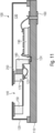
- Fig. 11
- shows a schematic side view of an innovative pressure transducer package with a rigid transfer block comprising an assembly tolerance portion according to a further embodiment, and
- Fig. 12
- shows a schematic block diagram of an innovative method for manufacturing a pressure transducer package according to an embodiment
- Equal or equivalent elements or elements with equal or equivalent functionality are denoted in the following description by equal or equivalent reference numerals.
- Method steps which are depicted by means of a block diagram and which are described with reference to said block diagram may also be executed in an order different from the depicted and/or described order. Furthermore, method steps concerning a particular feature of a device may be replaceable with said feature of said device, and the other way around.
- In the following, MEMS sound transducers, and in particular MEMS microphones, may be described as non-limiting examples for MEMS pressure transducers in general. However, each embodiment described herein may comprise a general pressure transducer, such as an environmental pressure sensor or the like.
- For introductory purposes,
Figure 1A shows aMEMS microphone package 10 in a standard top-port configuration. Thepackage 10 comprises asubstrate 11. Alid 12 is attached to thesubstrate 11, such that acavity 13 is formed between thelid 12 and thesubstrate 11. - In this top-port configuration, the
lid 12 comprises anopening 14 through which thecavity 13 is in fluid communication with a package-external environment, i.e. theopening 14 allows for a fluid exchange between an interior and an exterior of thecavity 13. Thus, theopening 14 may also be referred to as a fluid port. In case of a MEMS microphone package, as exemplarily described here, theopening 14 may also be referred to as a sound port. - A
MEMS microphone 15 is arranged inside thecavity 13. TheMEMS microphone 15 may be attached to thesubstrate 11. Furthermore, thepackage 10 comprises aconductive package pad 16 for electrically contacting theMEMS microphone 15 from outside thepackage 10. - Electric conductors, such as
bond wires package pad 16 and theMEMS microphone 15. Optionally, a controllingcircuitry 21 may sit between thepackage pad 16 and theMEMS microphone 15 in said electric path. - In this exemplarily shown standard top-port configuration, sound waves may enter the
cavity 13 through thesound port 14 provided in thelid 12. The sound waves may impinge on themicrophone membrane 19 of theMEMS microphone 15, in response to which themicrophone membrane 19 oscillates. These oscillations create a corresponding electric signal that can be conducted through theelectric conductors available circuitry 21, to thepackage pad 16, from which the signal can be picked up from outside thepackage 10. - A free space underneath the
microphone membrane 19, i.e. between themicrophone membrane 19 and thesubstrate 11, may be referred to as a so-called backvolume 20. The larger theback volume 20, the better the sensitivity of theMEMS microphone 15 and its signal-to-noise ratio (SNR). However, as can be seen inFigure 1A , the size of theback volume 20 is limited by the size of the free space underneath themicrophone membrane 19. -
Figure 1B shows an alternative solution for providing alarger back volume 20. This exemplary configuration may be referred to as a so-called bottom-port configuration. Thesound port 14 is not provided in thelid 12, but in thesubstrate 11 instead. More particular, thesubstrate 11 comprises thesound port 14 which enables a fluid exchange between the interior and the exterior of thecavity 13. In this bottom-port configuration, theMEMS microphone 15 covers thesound port 14. - Compared to the top-port configuration of
Figure 1A , the bottom-port configuration ofFigure 1B provides a muchlarger back volume 20. In particular, theentire cavity 13 can be used as theback volume 20. Accordingly, theMEMS microphone 15 in the bottom-port configuration may comprise a better sensitivity and lower SNR than in the aforementioned top-port configuration. - As can be seen in
Figures 1A and1B , in both the top-port and the bottom-port configuration theMEMS microphone 15 is mounted on thesubstrate 11, and thepackage pad 16 is also provided in thesubstrate 11, i.e. theMEMS microphone 15 and thepackage pad 16 are arranged on the same side (i.e. the substrate-side) of thepackage 10. Accordingly, in the package assembly process thesubstrate 11 can be completely pre-assembled before thelid 12 is attached, i.e. all components, such as theMEMS microphone 15, the controllingcircuitry 21, etc. may be placed and mounted on thesubstrate 11 before finally mounting thelid 12 onto thesubstrate 11. - However, in some instances it may be necessary to position the
MEMS microphone 15 and thepackage pad 16 on two opposite sides of thepackage 10. Such situations may appear if only limited available mounting space dictates a certain mounting position of thepackage 10 inside an electronic device (e.g. smartphone). - For example,
Figure 1C shows a flipped top-port configuration, in which thepackage pad 16 may be provided on thesubstrate 11, while theMEMS microphone 15 may be attached to thelid 12 for covering thesound port 14 formed therein. - In this situation, the
substrate 11 cannot be completely pre-assembled during the package assembly process, i.e. before thelid 12 is attached. As soon as thelid 12 is attached to thesubstrate 11, thepackage 10 is closed such that the interior 13 of thepackage 10 cannot be accessed anymore. Accordingly, there is no possibility to provide flexible bond wires for connecting the MEMS microphone 15 (lid-side) with the opposite package pad 16 (substrate-side) since it is not possible anymore to access theinterior 13 of theclosed package 10. - Existing solutions suggest providing stiff and rigid connection means for providing a physical and electrical contact between the
MEMS microphone 15 and thepackage pad 16. Thus, if the package is closed, stiff connection means may provide a mechanical and electrical contact comparable to a plug and socket connection. - However, due to the rigid nature of stiff connection means, the
MEMS microphone 15 has to be placed very precisely (preferably without any assembly tolerances) at its intended mounting position. Even smallest assembly tolerances, which are not avoidable in real life, may cause a statically overdefined indeterminate mechanical system leading to undesired faults and breakages of the stiff connection means. For example, the distance d between thelid 12 and thesubstrate 11 is dictated by the height h of thelid 12 and the thickness t of the applied mounting means 22 (e.g., adhesives, solder, etc.). If stiff and rigid connection means were applied between theMEMS microphone 15 and thepackage pad 16, they would have to have an extremely precise shape and length in order to exactly fit the distance d. Otherwise, they would either be too short thereby failing to provide a proper electric connection, or they would be too large causing an obstruction such that thelid 12 cannot be properly closed. Both cases describe a statically overdefined indeterminate mechanical system. - Therefore, it is desirable to provide a solution for a MEMS package configuration having the
MEMS microphone 15 and thepackage pad 16 arranged on two opposite package-sides, which solution allows for mounting thelid 12 to thesubstrate 11 with a certain assembly tolerance such that thepackage 10 is provided as a statically underdefined indeterminate mechanical system. -
Figure 2 shows a first embodiment of the herein disclosed solution regarding apressure transducer package 100 comprising an innovative opposite-port-pad configuration. Thepackage 100 comprises asubstrate 110 and alid 120 being attached to thesubstrate 110. Acavity 130 is defined between thesubstrate 110 and thelid 120, i.e. underneath thelid 120. Thelid 120 may be attached to thesubstrate 110 by means of solder and/orglue - A
MEMS pressure transducer 150 is arranged inside thecavity 130. According to this non-limiting example, theMEMS pressure transducer 150 may be configured as a MEMS sound transducer, and in particular as a MEMS microphone. However, theMEMS pressure transducer 150 may also be configured as a MEMS speaker, a MEMS ambient pressure sensor, or any other kind of MEMS pressure transducer. - The
package 100 further comprises afluid port 140 for allowing a fluid exchange between an interior and an exterior of thecavity 130, wherein theMEMS pressure transducer 150 is mounted such that it covers saidfluid port 140. In this non-limiting example, thefluid port 140 is provided in thelid 120. However, it may also be possible that thefluid port 140 may be provided in thesubstrate 110, examples of which may be described somewhat later in this description. In case theMEMS pressure transducer 150 is configured as a sound transducer, thefluid port 140 may also be referred to as a sound port. - The
package 100 further comprises aconductive package pad 160 for electrically contacting theMEMS pressure transducer 150 from outside thepackage 100. According to the innovative opposite-port-pad configuration, thepackage pad 160 and thefluid port 140 are positioned on twoopposite sides package 100, i.e. thepackage pad 160 may be provided at afirst side 101 of thepackage 100, while thefluid port 140 may be provided at an oppositesecond side 102 of thepackage 100. More particular, thefluid port 140 may be provided in (or at) at least one of thelid 120 and thesubstrate 110, while thepackage pad 160 may be provided in (or at) the other one of thelid 120 and thesubstrate 110. According to the non-limiting example shown inFigure 2 , thefluid port 140 is provided in thelid 120, while thepackage pad 160 is provided in thesubstrate 110. - Since the
MEMS pressure transducer 150 is mounted directly at thefluid port 140, i.e. such that it covers thefluid port 140, theMEMS pressure transducer 150 and thepackage pad 160 may also be positioned on twoopposite sides package 100. Nevertheless, theMEMS pressure transducer 150 has to be electrically connected somehow to the oppositely arrangedpackage pad 160. - However, as mentioned above, when the
lid 120 is finally mounted and attached to thesubstrate 110 during the assembly process, thepackage 100 is closed, while inside the closed package 100 a physical gap remains between theMEMS pressure transducer 150 on the onepackage side 101 and thepackage pad 160 on the oppositeother package side 102. As mentioned above, this gap needs to be bridged somehow with an electric conductor for electrically connecting theMEMS pressure transducer 150 with the oppositely positionedpackage pad 160. However, since thepackage 100 is closed it is not accessible anymore and, thus, it is not possible to subsequently provide flexible electric conductors (e.g., bond wires, etc.) inside theclosed package 100 for connecting theMEMS pressure transducer 150 with thepackage pad 160. - Therefore, the
innovative package 100 comprises arigid transfer block 180 that is arranged inside thecavity 130, therigid transfer block 180 being configured to provide an electric path between theMEMS pressure transducer 150 and the oppositely arrangedpackage pad 160. - According to the innovative principle, the
rigid transfer block 180 is configured to provide an assembly tolerance between theMEMS pressure transducer 150 and thepackage pad 160 upon assembly of thepackage 100, such that the lid 120 (including the MEMS pressure transducer 150) can be mounted and attached to thesubstrate 110 with a certain assembly tolerance. Therefore, according to an embodiment, therigid transfer block 180 comprises anassembly tolerance portion 170. Theassembly tolerance portion 170 provides a mechanical assembly tolerance between therigid transfer block 180 and thesubstrate 110, and/or between therigid transfer block 180 and thelid 120. - Additionally or alternatively, the
lid 120 may comprise anassembly tolerance portion 170. Also in this case, theassembly tolerance portion 170 may provide a mechanical assembly tolerance between therigid transfer block 180 and thelid 120, examples and embodiments of which will be described somewhat later. - Since the
assembly tolerance portion 170 provides a mechanical assembly tolerance, theassembly tolerance portion 170 allows for a relative displacement / misalignment between the lid 120 (including any components arranged thereon) and the substrate 110 (including any components arranged thereon) during assembly of thepackage 100, while still properly establishing an electric path between theMEMS pressure transducer 150 and the oppositely arrangedpackage pad 160. In other words, the electric path between theMEMS pressure transducer 150 and the oppositely arrangedpackage pad 160 may still be properly established even if thelid 120 was attached to thesubstrate 110 with some misalignment. This is due to the fact that some predetermined assembly tolerance may be provided by theassembly tolerance portion 170. - When assembling a package in an opposite-port-pad configuration, actually flexible electric connectors (e.g., bond wires) would be favorable between the
MEMS pressure transducer 150 and the oppositely arrangedpackage pad 160 in order to allow for a relative displacement / misalignment between thelid 120 and thesubstrate 110. However, flexible connectors cannot be subsequently provided after thepackage 100 is closed. A rigid connector (plug-and-socket), instead, can be easily provided prior to attaching thelid 120 to thesubstrate 110. However, a rigid connector must comprise a very exact shape and/or length in order to allow a proper attachment of thelid 120 on thesubstrate 110. If a rigid connector was too big, it would cause an obstruction such that thelid 120 would not fit anymore and would protrude from thesubstrate 110. If a rigid connector was too small, instead, the electric path inside theclosed package 100 could not be properly established between theMEMS pressure transducer 150 and thepackage pad 160. - Stated in more technical terms, flexible connectors would provide a statically underdefined indeterminate mechanical system, which is desirable for opposite-port-pad configurations since it allows for some assembly tolerance or misalignment. However, they cannot be subsequently installed. Rigid connectors, instead, may be easy to install but would provide a statically overdefined indeterminate mechanical system.
- The herein described innovative concept combines the advantages of both connecting principles. Even though the
transfer block 180 is rigid, the innovativeassembly tolerance portion 170 allows for some displacement/ misalignment between thelid 120 and thesubstrate 110. In other words, even though thetransfer block 180 is rigid, the additionalassembly tolerance portion 170 provides for a statically underdefined indeterminate mechanical system. This explanation refers to a static mechanical system, in which thelid 120, therigid transfer block 180 and thesubstrate 110 are mechanically connected to each other. - The
assembly tolerance portion 170 even allows for some misalignment of therigid transfer block 180 itself. As can be seen in the example shown inFigure 2 , therigid transfer block 180 may be mounted between thesubstrate 110 and thelid 120. Therigid transfer block 180 may be fixedly attached to at least one (or exactly one) of thesubstrate 110 and thelid 120. In the example shown inFigure 2 , thetransfer block 180 may be fixedly attached (e.g., by means of glue) to the inside of thelid 120. In alternative embodiments, which will be explained later, therigid transfer block 180 may be fixedly attached to thesubstrate 110. In any case, the position at which thetransfer block 180 is fixedly mounted / attached is referred to as its predetermined mounting position. Theassembly tolerance portion 170 allows to keep therigid transfer block 180 at its predetermined mounting position, even if thelid 120 and thesubstrate 110 were misaligned during assembly. - As exemplarily depicted in
Figure 2 , an electric path may be provided inside thepackage 100 between theMEMS pressure transducer 150 and the oppositely arrangedpackage pad 160. In particular, thetransfer block 180 may be configured to provide the electric path between theMEMS pressure transducer 150 and the oppositely arrangedpackage pad 160. Therefore, thetransfer block 180 may be electrically connected to theMEMS pressure transducer 150 and thepackage pad 160, e.g., by means of rigid or flexible connectors, such as wire bonds 121. - A
wire bond connection 121 between theMEMS pressure transducer 150 and therigid transfer block 180 may be easily provided since both are arranged on the same package-side, e.g. at thelid 120, such that a pre-assembly is possible before finally closing thepackage 100. - In order to keep the length of the
conductive connector 121 as short as possible, thetransfer block 180 may be mounted directly adjacent to theMEMS pressure transducer 150, without any further components in between. A short length of theconductive connector 121 may enhance the RF stability, since a shortconductive connector 121 is less prone to RF interference. - For example, a first conductive path may be provided between the
rigid transfer block 180 and theMEMS pressure transducer 150, and a second conductive path may be provided between therigid transfer block 180 and thepackage pad 160. The first and second conductive paths may be parts of the electric path between theMEMS pressure transducer 150 and thepackage pad 160. - Optionally, a controlling circuitry 190 (e.g., an ASIC) for controlling the
MEMS pressure transducer 150 may be arranged inside thepackage 100, wherein the controllingcircuitry 190 may sit in the electric path between theMEMS pressure transducer 150 and thepackage pad 160. The controllingcircuitry 190 may be coupled to the electric path by means of electric conductors, such as wire bonds, as exemplarily depicted inFigure 2 , or via flip-chip bonding. - However, the controlling
circuitry 190 is optional since it may also be arranged outside thepackage 100, where it would not sit in the electric path between theMEMS pressure transducer 150 and thepackage pad 160. Accordingly, even though it is exemplarily depicted inFigure 2 that therigid transfer block 180 may be coupled to an internalcontrolling circuitry 190, therigid transfer block 180 may be directly coupled to thepackage pad 160. - Any electric connections on the
substrate 110 may be provided by means of a conductive wiring provided in or at thesubstrate 110. Said wiring may comprise at least one ofconducting wire bonds 122, conductingsurface pads 123, conducting surface traces (not shown) and conductinglayers 124 integrated into thesubstrate 110. Thesubstrate 110 may be a Printed Circuit Board (PCB). - In the same way, the
transfer block 180 may comprise at least one of the above mentioned electric conductors. For example, thetransfer block 180 may be made of, or may comprise, a material similar to a Printed Circuit Board (PCB), such as resin, wherein one or moreelectric conductors 125 may be implemented in one or more layers of thetransfer block 180. Additionally or alternatively, therigid transfer block 180 may comprise at least one ofconductive surface pads 126 and conductive surface traces 125. - In the embodiment shown in
Figure 2 , therigid transfer block 180 is firmly attached to thelid 120 and spaced apart from thesubstrate 110, wherein a physical gap remains between therigid transfer block 180 and thesubstrate 110. In this exemplary embodiment, theassembly tolerance portion 170 may comprise aconductive pin 171 for bridging the gap and for providing a conductive path between therigid transfer block 180 and thesubstrate 110. - The
assembly tolerance portion 170 may further comprise arecess 172 provided in therigid transfer block 180, wherein theconductive pin 171 is, at least partly, arranged inside saidrecess 172. Therecess 172 may be wider than a width of theconductive pin 171, such that theconductive pin 171 is accommodated inside therecess 172 by a clearance-fit. Thus, when attaching thelid 120 to thesubstrate 110, thepin 171 can move inside therecess 172 in a clearance-fit manner, thereby providing an assembly tolerance that allows for a misalignment of thelid 120 relative to thesubstrate 110. - Additionally or alternatively to the above discussed
recess 172 provided in thetransfer block 180, arecess 173 may be provided in thesubstrate 110. Therecesses conductive pin 171 may be, at least partly, arranged inside saidrecess 173 in thesubstrate 110. Therecess 173 in thesubstrate 110 may be wider than a width of theconductive pin 171, such that theconductive pin 171 is accommodated inside therecess 173 by a clearance-fit. Thus, when attaching thelid 120 to thesubstrate 110, thepin 171 can move inside therecess 173 in a clearance-fit manner, thereby providing an assembly tolerance that allows for a misalignment of thelid 120 relative to thesubstrate 110. - Optionally, a clearance between the
conductive pin 171 and therecess 172, and/or a clearance between theconductive pin 171 and therecess 173, may be filled with conductive filler material, for example solder, solder paste, or a conductive adhesive. For example, a conductive adhesive may comprise an anisotropically conductive adhesive material (ACA) or an anisotropically conductive film material (ACF). In this case, therecesses - The conductive filler material may be elastic, at least prior to or during assembly of the
package 100. For example, the conductive filling material may comprise an adhesive that is elastic, at least prior to curing. The filling material may be applied to therecess lid 120 to thesubstrate 110. The filling material may be liquid, pasty or viscous. After assembly, i.e. after thelid 120 has been attached to thesubstrate 110, the filler material may cure, wherein the filler material may remain elastic or may become inelastic at room temperature. For example, an adhesive may be permanently elastic at room temperature even after curing, or it may be temporarily elastic at room temperature such that it becomes stiff and inelastic after curing. For example, thebonding material 250 may comprise a permanently elastic soft glue. - Alternatively, the filler material may be solid at room temperature. Then, the filler material can be heated such that the filer material becomes liquid, pasty or viscous. For example, if the filler material comprises solder, then the
package 100 may undergo a thermal reflow process in which the solder is heated such that it gets viscous. In this state, theconductive pin 171 may be easily inserted into the viscous filler material contained in therecesses - For example, prior to assembly, the
conductive pin 171 may be inserted into therecess 172 provided in thetransfer block 180. During this pre-assembly stage, theconductive pin 171 may be fixedly secured inside therecess 172, e.g. by means of the conductive filler material (e.g. solder or glue). When attaching thelid 120 to thesubstrate 110, theconductive pin 171 may be inserted into theopposite recess 173 provided in thesubstrate 110. After thelid 120 has been attached to thesubstrate 110, theconductive pin 171 may be fixedly secured inside theopposite recess 173, e.g. by means of the conductive filler material. - In an alternative embodiment, which is not explicitly depicted, the
conductive pin 171 may be omitted. In this case, theassembly tolerance portion 170 may comprise therecesses lid 120 is attached to thesubstrate 110, the filler material contained in one of therecesses recesses package 100 may undergo a thermal reflow process in which the solder is heated such that it gets viscous. Accordingly, the solder contained in the tworecesses - In
Figure 2 , theconductive pin 171 may be formed as a straight and rigid pin, i.e. theconductive pin 171 may not be flexible.Figure 3 shows an alternative configuration of theconductive pin 171, wherein like elements with like or similar functionality as inFigure 2 are denoted with like reference numerals. -
Figure 3 shows a further embodiment of thepackage 100, wherein like elements with like or similar functionality as inFigure 2 are denoted with like reference numerals. According to this embodiment, theMEMS pressure transducer 150 covering thefluid port 140 may be arranged at or on thelid 120, while thepackage pad 160 may be arranged at or on thesubstrate 110. Thus, theMEMS pressure transducer 150 and thepackage pad 160 are arranged on two opposite sides of thepackage 100. -
Figure 3 shows aconductive pin 171 comprising abent portion 174 for providing a higher flexibility to theconductive pin 171 compared to a straight pin. For example, theconductive pin 171 may be provided as a bent metal piece to accommodate process tolerances. Thebent portion 174 enhances the flexibility of thepin 171 in a vertical direction, i.e. a direction between thelid 120 and thesubstrate 110. This flexibility allows a further degree of freedom in providing an assembly tolerance by means of theassembly tolerance portion 170. - It may be sufficient if the
assembly tolerance portion 170 may comprise exactly onesingle transfer block 180 and/or exactly onesingle pin 171 as discussed above with reference toFigures 2 and3 . Alternatively, two ormore pins 171 may be provided with or without the above discussedbent portion 174. The two ormore pins 171 may be arranged in a respective number of further recesses provided in thetransfer block 180. Alternatively, the two ormore pins 171 may be arranged inside a respective number of recesses provided in two or more transfer blocks 180. In turn, the two ormore pins 171 may be arranged in a respective number of further recesses provided in thesubstrate 110. -
Figure 4 shows a further embodiment of thepackage 100, wherein like elements with like or similar functionality as inFigures 2 and3 are denoted with like reference numerals. According to this embodiment, theMEMS pressure transducer 150 covering thefluid port 140 may be arranged at or on thelid 120, while thepackage pad 160 may be arranged at or on thesubstrate 110. Thus, theMEMS pressure transducer 150 and thepackage pad 160 are arranged on two opposite sides of thepackage 100. - In this embodiment, the
conductive pin 171 may comprise abent portion 174. Alternatively, theconductive pin 171 may be formed as a straight and rigid pin, as shown inFigure 2 . - A difference compared to the previous Figures is the additional
environmental barrier structure 210 that may cover thefluid port 140 from the outside of thelid 120. Theenvironmental barrier structure 210 may act as a mechanical barrier against ingress of dust, fluids, solid matter, and the like, that may otherwise cause mechanical damage of theMEMS membrane 151. Theenvironmental barrier structure 210 may be provided as a stiff rigid mesh or as a compliant / flexible membrane. - The
environmental barrier structure 210 may be integrated into thelid 120 to avoid costly laser cavity structuring, which otherwise needs to be done if theenvironmental barrier structure 210 was integrated into, or attached to, thesubstrate 110. Therefore, thelid 120 may comprise a recess orindentation 220 at its outer surface in which theenvironmental barrier structure 210 may be accommodated. -
Figure 5 shows a further embodiment of thepackage 100, wherein like elements with like or similar functionality as in the previous Figures are denoted with like reference numerals. According to this embodiment, theMEMS pressure transducer 150 covering thefluid port 140 may be arranged at or on thelid 120, while thepackage pad 160 may be arranged at or on thesubstrate 110. Thus, theMEMS pressure transducer 150 and thepackage pad 160 are arranged on two opposite sides of thepackage 100. - In this embodiment, the
conductive pin 171 may either comprise abent portion 174, as depicted inFigure 3 , or theconductive pin 171 may be formed as a straight and rigid pin, as depicted inFigure 2 . - A difference compared to the previously discussed embodiments is the
additional insulation structure 230 provided at the outer circumference of theconductive pin 171. Theinsulation structure 230 may protect theconductive pin 171 from shorting. -
Figure 6 shows a further embodiment of thepackage 100, wherein like elements with like or similar functionality as in the previous Figures are denoted with like reference numerals. According to this embodiment, theMEMS pressure transducer 150 covering thefluid port 140 may be arranged at or on thelid 120, while thepackage pad 160 may be arranged at or on thesubstrate 110. Thus, theMEMS pressure transducer 150 and thepackage pad 160 are arranged on two opposite sides of thepackage 100. - According to this embodiment, the
rigid transfer block 180 may be configured as one integral part extending gaplessly between thelid 120 and thesubstrate 110, i.e. there is no physical gap remaining between thetransfer block 180 and thesubstrate 110. Furthermore, theMEMS pressure transducer 150 is mounted on thelid 120 such that it covers thefluid port 140 provided in thelid 120. Thepackage pad 160 is provided at thesubstrate 110 and, thus, arranged on an opposite side of theMEMS pressure transducer 150. - In this embodiment, the
rigid transfer block 180 may comprise anassembly tolerance portion 170. Theassembly tolerance portion 170 may comprise anaccommodating portion 175 being provided at therigid transfer block 180, wherein saidaccommodating portion 175 may be accommodated in ahole 128 provided in thelid 120. Theaccommodating portion 175 may be provided as a protruding portion that protrudes from a surface of thetransfer block 180. Theaccommodating portion 175 may be provided at an upper surface of thetransfer block 180 that faces thelid 120. Theaccommodating portion 175 may be inserted into thehole 128 in thelid 120. Theaccommodating portion 175 may be flush with the outer surface of thelid 120. - Additionally or alternatively (not shown here), the
rigid transfer block 180 may comprise an accommodating portion being provided at a lower surface of thetransfer block 180 that faces thesubstrate 110. This accommodating portion may be accommodated in a hole provided in thesubstrate 110. Theaccommodating portion 175 may be inserted into the hole in thesubstrate 110. - The
hole 128 in thelid 120 and/or in thesubstrate 110 may be wider than a width of theaccommodating portion 175, such that theaccommodating portion 175 is accommodated inside thehole 128 by a clearance-fit. Theaccommodating portion 175 of thetransfer block 180 may comprise a width that may be 1.2 times to 1.8 times smaller than the width of thehole 128. For example, thehole 128 in thelid 120 may comprise a width between 0.7 mm and 0.8 mm, while theaccommodating portion 175 may comprise a width between 0.4 mm and 0.6 mm. Accordingly, a clearance between theaccommodating portion 175 and thehole 128 in thelid 120 may be between 0.1 mm and 0.4 mm. - A clearance between the
accommodating portion 175 and thehole 128 may be filled withbonding material 250, in particular with non-conductive bonding material, such as glue. For example, thenon-conductive bonding material 250 may be permanently elastic, such that it is elastic prior to and after curing. For example, thebonding material 250 may comprise a permanently elastic soft glue. Alternatively, thenon-conductive bonding material 250 may be temporarily elastic, such that it is elastic prior to curing but non-elastic after curing. - In a pre-assembly step, the
accommodating portion 175 bearing thebonding material 250 may be loosely inserted into thehole 128. Accordingly, also therigid transfer block 180 would then be loosely attached to thelid 120. Therigid transfer block 180 can be electrically coupled, e.g. by means ofbond wires 121, to theMEMS pressure transducer 150 that may be fixedly secured to thelid 120. During assembly, i.e. after attaching thelid 120 to thesubstrate 110, thetransfer block 180 can be fixedly secured to thelid 120, e.g. by curing thenon-conductive bonding material 250. Therigid transfer block 180 may then be electrically coupled, and fixedly secured, to thesubstrate 110 by means ofsolder 240 using a thermal reflow process. - Alternatively, the
rigid transfer block 180 may be attached to, and fixedly secured, to thesubstrate 110 in a pre-assembly step, e.g. by means of solder orglue 240. During assembly, thelid 120 can be attached to thesubstrate 110 such that thehole 128 in thelid 120 is positioned opposite to theaccommodating portion 175 of therigid transfer block 180. When attaching thelid 120 to thesubstrate 110, thehole 128 in thelid 120 can be put over theaccommodating portion 175 bearing thebonding material 250. The clearance-fit between theaccommodating portion 175 and thehole 128 provides a mechanical assembly tolerance, such that thelid 120 can be attached to thesubstrate 110 with some misalignment. -
Figure 7 shows a further embodiment of thepackage 100, wherein like elements with like or similar functionality as in the previous Figures are denoted with like reference numerals. According to this embodiment, theMEMS pressure transducer 150 covering thefluid port 140 may be arranged at or on thesubstrate 110, while thepackage pad 160 may be arranged at or on therigid transfer block 180, in particular at a surface of thetransfer block 180 facing away from thesubstrate 110. Thus, theMEMS pressure transducer 150 and thepackage pad 160 are arranged on two opposite sides of thepackage 100. - In contrast to previously discussed
Figure 6 , thefluid port 140 is provided in thesubstrate 110, e.g. formed as a through hole extending between two opposite surfaces of thesubstrate 110. TheMEMS pressure transducer 150 is mounted on thesubstrate 110 such that it covers thefluid port 140. - According to the embodiment as shown in
Figure 7 , therigid transfer block 180 may be configured as one integral part extending gaplessly between thelid 120 and thesubstrate 110, i.e. there is no physical gap remaining between thetransfer block 180 and thesubstrate 110. - The
assembly tolerance portion 170 may comprise anaccommodating portion 175 being provided at therigid transfer block 180, wherein saidaccommodating portion 175 may be accommodated in ahole 128 provided in thelid 120. Regarding therigid transfer block 180, theaccommodating portion 175, thehole 128 and thebonding material 250, it is to be noted that everything that was mentioned before, with reference toFigure 6 , correspondingly applies to the embodiment ofFigure 7 . - However, in the embodiment of
Figure 7 , thepackage pad 160 may be arranged at therigid transfer block 180, and in particular at theaccommodating portion 175 accommodated inside thehole 128 in thelid 120. Thepackage pad 160 may protrude from thehole 128 in thelid 120 for being externally contactable from outside thepackage 100. - At the opposite side of the
rigid transfer block 180, i.e. the side that faces thesubstrate 110, therigid transfer block 180 may be electrically and mechanically coupled to thesubstrate 110 by means of a bonding means 260, such as solder or glue. For example, therigid transfer block 180 may be coupled to asurface pad 260 provided at a surface of thesubstrate 110. Anintegrated conducting layer 124 may electrically connect thesurface pad 260 with theMEMS pressure transducer 150, wherein the aforementionedintegrated circuitry 190 may optionally sit in between. - As mentioned before, conducting surface pads, conducting surface traces and integrated conducting layers may be part of the wiring of the
substrate 110. Accordingly, stated in more general terms, therigid transfer block 180 may be conductively coupled to a wiring being provided in or at thesubstrate 110 for establishing the electric path between thepackage pad 160 and the oppositely arrangedMEMS pressure transducer 150. -
Figure 8 shows a further embodiment of thepackage 100, wherein like elements with like or similar functionality as in the previous Figures are denoted with like reference numerals. According to this embodiment, theMEMS pressure transducer 150 covering thefluid port 140 may be arranged at or on thesubstrate 110, while thepackage pad 160 may be arranged at or on therigid transfer block 180, in particular at a surface of thetransfer block 180 facing away from thesubstrate 110. Thus, theMEMS pressure transducer 150 and thepackage pad 160 are arranged on two opposite sides of thepackage 100. - In contrast to previously discussed
Figure 7 , therigid transfer block 180 may comprise aconductive connection pad 270 for establishing the electric path between thepackage pad 160 and theMEMS pressure transducer 150, wherein theconductive connection pad 270 is spatially and galvanically separated from thesubstrate 110. - For example, the
rigid transfer block 180 may comprise a protrudingportion 181 at which theconductive connection pad 270 may be arranged. The protrudingportion 181 may laterally protrude from the contour of therigid transfer block 180. Theconductive connection pad 270 may be arranged at said protrudingportion 181 such that the protrudingportion 181 is positioned between theconductive connection pad 270 and thesubstrate 110. - The electric path between the
package pad 160 and the oppositely arrangedMEMS pressure transducer 150 may be established byelectric connectors 121, such as bond wires, for example. Theelectric connectors 121 may be connected to theconductive connection pad 270. Theconductive connection pad 270 and thepackage pad 160 may be electrically coupled to each other by means of wirings provided in or at therigid transfer block 180. Accordingly, by connecting theMEMS pressure transducer 150 to theconductive connection pad 270, theMEMS pressure transducer 150 is also coupled to thepackage pad 160. Optionally, a controllingcircuitry 190 may sit in the electric path between theMEMS pressure transducer 150 and thepackage pad 160. - According to the embodiment shown in
Figure 8 , thesubstrate 110 may be configured as a wiring-less substrate, i.e. thesubstrate 110 does not need to be equipped with expensive wirings, such as surface pads, surface traces or integrated conductive layers. A simple plastics substrate may be sufficient in this case. -
Figure 9 shows a further embodiment of thepackage 100, wherein like elements with like or similar functionality as in the previous Figures are denoted with like reference numerals. According to this embodiment, theMEMS pressure transducer 150 covering thefluid port 140 may be arranged at or on thelid 120, while thepackage pad 160 may be arranged at or on thesubstrate 110. Thus, theMEMS pressure transducer 150 and thepackage pad 160 are arranged on two opposite sides of thepackage 100. - The
rigid transfer block 180 may be similar to the embodiments discussed with reference toFigure 6 . However the embodiment ofFigure 8 can be combined with each embodiment in which therigid transfer block 180 is coupled to thelid 120. - As can be seen in
Figure 9 , thelid 120 comprises one or moreflexible tongues flexible tongues lid 120. For example, the one or moreflexible tongues lid 120, and by bending the remaining lid material portions to the inside, i.e. in the direction of thecavity 130. - Due to the flexible nature of the
flexible tongues flexible tongues flexible tongues assembly tolerance portion 170. In the previously discussed embodiments, theassembly tolerance portion 170 was part of therigid transfer block 180. However, additionally or alternatively, theassembly tolerance portion 170 may comprise the above discussedflexible tongues lid 120. - The resilient or
flexible tongues lid 120 and thesubstrate 110. In other words, the resilient orflexible tongues - The one or more
flexible tongues rigid transfer block 180, e.g. by means ofnon-conductive bonding material 250, such as glue. Thebonding material 250 may be permanently or temporarily elastic, as discussed above. For example, thebonding material 250 may comprise a permanently elastic soft glue. As long as thebonding material 250 is flexible, it allows for a lateral misalignment, i.e. it provides a lateral assembly tolerance. - In a pre-assembly step, i.e. prior to attaching the
lid 120 to thesubstrate 110, thetransfer block 180 may be attached to theflexible tongues bonding material 250. Thetransfer block 180 may be loosely attached to thetongues bonding material 250 is flexible prior to curing. During assembly, i.e. when thelid 120 gets attached to thesubstrate 110, theflexible tongues flexible bonding material 250 allow for a compensation of lateral and vertical assembly misalignments. After thelid 120 has been attached to thesubstrate 110, thebonding material 250 may be cured. -
Figure 10 shows a further embodiment of thepackage 100, wherein like elements with like or similar functionality as in the previous Figures are denoted with like reference numerals. According to this embodiment, theMEMS pressure transducer 150 covering thefluid port 140 may be arranged at or on thelid 120, while thepackage pad 160 may be arranged at or on thesubstrate 110. Thus, theMEMS pressure transducer 150 and thepackage pad 160 are arranged on two opposite sides of thepackage 100. - According to this embodiment, the
assembly tolerance portion 170 may comprise asolder connector 280, such as a stud bump or a solder ball. During assembly, i.e. while attaching thelid 120 to thesubstrate 110, thepackage 100 can undergo a thermal reflow process such that thesolder connector 280 is heated to its reflow temperature at which it begins to slightly flow. At this stage, theviscous solder connector 280 allows for a movement of thetransfer block 180 thereby providing a certain assembly tolerance. - The
transfer block 180 may comprise aconductive connection pad 260 via which it is conductively coupled to thesolder connector 280. Thesolder connector 280 may be conductively coupled with thesubstrate 110 by means of the wiring of thesubstrate 110, e.g. by means of a conductive surface pad, or the like. - In a pre-assembly step, the
MEMS pressure transducer 150 and thetransfer block 180 may be arranged at the inside of thelid 120, preferably directly adjacent to each other. TheMEMS pressure transducer 150 may be electrically coupled with thetransfer block 180 via a flexible connector, such as abond wire 121. Accordingly, thelid 120 comprising theMEMS pressure transducer 150 and therigid transfer block 180 can be pre-assembled before thelid 120 is attached to thesubstrate 110. -
Figure 11 shows a further embodiment of thepackage 100, wherein like elements with like or similar functionality as in the previous Figures are denoted with like reference numerals. According to this embodiment, theMEMS pressure transducer 150 covering thefluid port 140 may be arranged at or on thelid 120, while thepackage pad 160 may be arranged at or on thesubstrate 110. Thus, theMEMS pressure transducer 150 and thepackage pad 160 are arranged on two opposite sides of thepackage 100. - In this embodiment, the
rigid transfer block 180 may be firmly attached to thesubstrate 110 and indirectly attached to thelid 120 via theMEMS pressure transducer 150, wherein theassembly tolerance portion 170 may be provided between therigid transfer block 180 and theMEMS pressure transducer 150. - The
assembly tolerance portion 170 may comprise abonding material 250, and in particular a non-conductive bonding material, such as glue. Thebonding material 250 may be permanently elastic, such that it is elastic prior to and after curing. For example, thebonding material 250 may comprise a permanently elastic soft glue. Alternatively, thenon-conductive bonding material 250 may be temporarily elastic, such that it is elastic prior to curing but non-elastic after curing. - In a further embodiment, that is not explicitly depicted here, the
MEMS pressure transducer 150 may be attached to thesubstrate 110. Therigid transfer block 180 may be firmly attached to thelid 120 and indirectly attached to thesubstrate 110 via theMEMS pressure transducer 150. In this case, theassembly tolerance portion 170 may be provided between therigid transfer block 180 and theMEMS pressure transducer 150. - Mounting the
rigid transfer block 180 to thelid 120 via theMEMS pressure transducer 150 by means of a soft /flexible bonding material 250 may lower the mechanical stress. Thebonding material 250 may provide a fixation between thetransfer block 180 and theMEMS pressure transducer 150, which is stable enough to allow for an electric coupling of theMEMS pressure transducer 150 and thetransfer block 180 by flexible bonding means 121 during a pre-assembly step. - In each and every embodiment as discussed herein, the innovative
assembly tolerance portion 170 provides a mechanical assembly tolerance during assembly of thepackage 100. This solves the overdefinition problem, i.e. overdefinition of a statically indeterminate system can be avoided. Instead, the innovative assembly tolerance portion provides an underdefined statically indeterminate system. - In the herein discussed opposite-port-pad configuration, the
rigid transfer block 180 is firmly attached to one of thesubstrate 110 and thelid 120, while therigid transfer block 180 is (flexibly) attached to one of thesubstrate 110 and thelid 120 via theassembly tolerance portion 170. In other words, it may be sufficient when therigid transfer block 180 is coupled to one of thelid 120 and thesubstrate 110 by means of theassembly tolerance portion 170, even if therigid transfer block 180 is fixedly secured to the other one of thelid 120 and thesubstrate 110. - In some embodiments, the
assembly tolerance portion 170 may provide a clearance-fit between therigid transform block 180 and one of thesubstrate 110 and thelid 120. Any clearance between therigid transform block 180 and the one of thesubstrate 110 and thelid 120 may be filled with a conductive ornon-conductive bonding material 250, such as solder or glue. - The
bonding material 250 may be permanently elastic, such that it is elastic prior to and after curing. For example, thebonding material 250 may comprise a permanently elastic soft glue. Alternatively, thenon-conductive bonding material 250 may be temporarily elastic, such that it is elastic prior to curing but non-elastic after curing. - According to some embodiments, the
assembly tolerance portion 170 may comprise a permanentlyelastic bonding material 250 being applied to therigid transfer block 180 for permanently elastically attaching therigid transfer block 180 to at least one of thelid 120 and thesubstrate 110. - The herein described innovation may also comprise a corresponding method for manufacturing a
pressure transducer package 100 as described above. A schematic block diagram of a method according to an embodiment is depicted inFigure 12 . - As schematically illustrated by
block 101 the method may comprise a step of providing asubstrate 110 and alid 120, wherein one of thesubstrate 110 and thelid 120 comprises afluid port 140, and wherein the other one of thesubstrate 110 and thelid 120 comprises aconductive package pad 160. - As schematically illustrated by
block 102 the method may further comprise a step of mounting aMEMS pressure transducer 150 such that it covers thefluid port 140. - As schematically illustrated by
block 103 the method may further comprise a step of providing arigid transfer block 180, therigid transfer block 180 being configured to provide an electric path between theMEMS pressure transducer 150 and thepackage pad 160. - As schematically illustrated by
block 104 the method may further comprise a step of performing a pre-assembly step in which theMEMS pressure transducer 150 is electrically coupled to therigid transfer block 180. - After the pre-assembly step, as schematically illustrated by
block 105, the method may further comprise a step of closing thepackage 100 by attaching thelid 120 to thesubstrate 110 such that thepackage pad 160 is provided at afirst side 101 of thepackage 100, while thefluid port 140 is provided at an oppositesecond side 102 of thepackage 100. - As schematically illustrated by
block 106 the method may further comprise a step of providing anassembly tolerance portion 170 in or at at least one of thelid 120 and therigid transfer block 180 for providing a mechanical assembly tolerance between therigid transfer block 180 and at least one of thesubstrate 110 and thelid 120 during the step of attaching thelid 120 to thesubstrate 110. Theassembly tolerance portion 170 is provided prior to attaching thelid 120 to thesubstrate 110. - Although some aspects have been described in the context of an apparatus, it is clear that these aspects also represent a description of the corresponding method, where a block or device corresponds to a method step or a feature of a method step. Analogously, aspects described in the context of a method step also represent a description of a corresponding block or item or feature of a corresponding apparatus.
- While this disclosure has been described with reference to illustrative embodiments, this description is not intended to be construed in a limiting sense. Various modifications and combinations of the illustrative embodiments, as well as other embodiments of this disclosure, will be apparent to persons skilled in the art upon reference to the description. It is therefore intended that the appended claims encompass any such modifications or embodiments.
Claims (20)
- A pressure transducer package (100) comprising:a substrate (110) and a lid (120) being attached to the substrate (110), wherein a cavity (130) is defined underneath the lid (120),a MEMS pressure transducer (150) arranged inside the cavity (130),a fluid port (140) for allowing a fluid exchange between an interior and an exterior of the cavity (130), the MEMS pressure transducer (150) covering said fluid port (140),a conductive package pad (160) for electrically contacting the MEMS pressure transducer (150) from outside the package (100),
wherein the package pad (160) is provided at a first side (101) of the package (100), while the fluid port (140) is provided at an opposite second side (102) of the package (100),a rigid transfer block (180) arranged inside the cavity (130), the rigid transfer block (180) being configured to provide an electric path between the MEMS pressure transducer (150) and the oppositely arranged package pad (160), andwherein at least one of the lid (120) and the rigid transfer block (180) comprises an assembly tolerance portion (170) for providing a mechanical assembly tolerance between the rigid transfer block (180) and at least one of the substrate (110) and the lid (120). - The pressure transducer package (100) according to claim 1,wherein the rigid transfer block (180) is mounted between the lid (120) and the substrate (110), andwherein the assembly tolerance portion (170) is configured to allow for a relative displacement between the substrate (110) and the lid (120) while keeping the rigid transfer block (180) at its predetermined mounting position during assembly of the package (100).
- The pressure transducer package (100) according to claim 1 or 2,wherein the rigid transfer block (180) is mounted between the lid (120) and the substrate (110), andwherein the assembly tolerance portion (170) is configured such that a static mechanical system, in which the lid (120), the rigid transfer block (180) and the substrate (110) are mechanically connected with each other, is statically indeterminate.
- The pressure transducer package (100) according to any one of claims 1 to 3,wherein the rigid transfer block (180) is attached to one of the substrate (110) and the lid (120) via the assembly tolerance portion (170), andwherein the rigid transfer block (180) is firmly attached to the other one of the substrate (110) and the lid (120).
- The pressure transducer package (100) according to any one of claims 1 to 4,
wherein the assembly tolerance portion (170) provides a clearance-fit between the rigid transform block (180) and one of the substrate (110) and the lid (120). - The pressure transducer package according to any one of claims 1 to 5,
wherein the assembly tolerance portion comprises a permanently elastic bonding material being applied to the rigid transfer block for permanently elastically attaching the rigid transfer block to at least one of the lid and the substrate. - The pressure transducer package (100) according to any one of claims 1 to 6,wherein the rigid transfer block (180) is firmly attached to the lid (120) and spaced apart from the substrate (110), wherein a gap remains between the rigid transfer block (180) and the substrate (110),wherein the assembly tolerance portion (170) comprises a conductive pin (171) for bridging the gap and for providing a conductive path between the rigid transfer block (180) and the substrate (110).
- The pressure transducer package (100) according to claim 7,
wherein the conductive pin (171) comprises a bent portion (174) for providing a higher flexibility to the conductive pin (171) compared to a straight pin. - The pressure transducer package (100) according to claim 7 or 8,wherein the assembly tolerance portion (170) comprises a recess (172) provided in the rigid transfer block (180), wherein the conductive pin (171) is, at least partly, arranged inside said recess (172),wherein the recess (172) is wider than a width of the conductive pin (171), such that the conductive pin (171) is accommodated inside the recess (172) by a clearance-fit, andwherein a clearance between the conductive pin (171) and the recess (172) is filled with conductive filler material.
- The pressure transducer package (100) according to any one of claims 7 to 9,wherein the conductive pin (171) is, at least partly, arranged inside a recess (173) provided in the substrate (110),wherein the recess (173) is wider than a width of the conductive pin (171), such that the conductive pin (171) is accommodated inside the recess (173) by a clearance-fit, andwherein a clearance between the conductive pin (171) and the recess (173) is filled with conductive filler material.
- The pressure transducer package (100) according to claim 9 or 10,
wherein the conductive filler material comprises at least one of solder, a solder paste and a conductive adhesive. - The pressure transducer package (100) according to any one of claims 7 to 11,
wherein the conductive pin (171) comprises an electric insulation structure (230) provided around the outer circumference of the conductive pin (171). - The pressure transducer package (100) according to any one of claims 1 to 6,wherein the rigid transfer block (180) is configured as an integral part extending gaplessly between the lid (120) and the substrate (110), andwherein the assembly tolerance portion (170) comprises an accommodating portion (175) being provided at the rigid transfer block (180), wherein said accommodating portion (175) is accommodated in a hole (128) provided in the lid (120),wherein the hole (128) in the lid (120) is wider than a width of the accommodating portion (175), such that the accommodating portion (175) is accommodated inside the hole (128) by a clearance-fit, andwherein a clearance between the accommodating portion (175) and the hole (128) is filled with bonding material (250).
- The pressure transducer package (100) according to claim 13,
wherein the package pad (160) is arranged at the accommodating portion (175) of the rigid transfer block (180), wherein the package pad (160) protrudes from the hole (128) in the lid (120) for being externally contactable from outside the package (100). - The pressure transducer package (100) according to any one of the preceding claims,
wherein the rigid transfer block (180) is conductively coupled to a wiring being provided in or at the substrate (110) for establishing the electric path between the package pad (160) and the oppositely arranged MEMS pressure transducer (150). - The pressure transducer package (100) according to any one of claims 1 to 14,
wherein the rigid transfer block (180) comprises a conductive connection pad (270) for establishing the electric path between the package pad (160) and the MEMS pressure transducer (150), wherein the conductive connection pad (270) is spatially and galvanically separated from the substrate (110). - The pressure transducer package (100) according to claim 16,
wherein the substrate (110) is configured as a wiring-less substrate. - The pressure transducer package (100) according to any one of the preceding claims,wherein the assembly tolerance portion (170) comprises one or more flexible tongues (221, 222) being integrally formed with the lid (120), andwherein said one or more flexible tongues (221, 222) are attached to the rigid transfer block (180).
- The pressure transducer package (100) according to any one of the preceding claims,wherein the MEMS pressure transducer (150) is attached to the lid (120),wherein the rigid transfer block (180) is arranged between the substrate (110) and the MEMS pressure transducer (150), wherein the rigid transfer block (180) is firmly attached to the substrate (110), andwherein the assembly tolerance portion (170) is provided between the rigid transfer block (180) and the MEMS pressure transducer (150).
- The pressure transducer package (100) according to any one of claims 1 to 18,wherein the MEMS pressure transducer (150) is attached to the substrate (110),wherein the rigid transfer block (180) is arranged between the lid (120) and the MEMS pressure transducer (150), wherein the rigid transfer block (180) is firmly attached to the lid (120), andwherein the assembly tolerance portion (170) is provided between the rigid transfer block (180) and the MEMS pressure transducer (150).
Priority Applications (3)
| Application Number | Priority Date | Filing Date | Title |
|---|---|---|---|
| EP23180426.1A EP4480898B1 (en) | 2023-06-20 | 2023-06-20 | A pressure transducer package comprising a rigid transfer block and an assembly tolerance portion |
| US18/644,368 US12630417B2 (en) | 2023-06-20 | 2024-04-24 | Pressure transducer package having a rigid transfer block for assembly tolerance |
| CN202410782735.8A CN119160849A (en) | 2023-06-20 | 2024-06-18 | Pressure transducer package including a rigid transfer block and an assembly tolerance portion |
Applications Claiming Priority (1)
| Application Number | Priority Date | Filing Date | Title |
|---|---|---|---|
| EP23180426.1A EP4480898B1 (en) | 2023-06-20 | 2023-06-20 | A pressure transducer package comprising a rigid transfer block and an assembly tolerance portion |
Publications (2)
| Publication Number | Publication Date |
|---|---|
| EP4480898A1 true EP4480898A1 (en) | 2024-12-25 |
| EP4480898B1 EP4480898B1 (en) | 2026-04-01 |
Family
ID=86904362
Family Applications (1)
| Application Number | Title | Priority Date | Filing Date |
|---|---|---|---|
| EP23180426.1A Active EP4480898B1 (en) | 2023-06-20 | 2023-06-20 | A pressure transducer package comprising a rigid transfer block and an assembly tolerance portion |
Country Status (2)
| Country | Link |
|---|---|
| EP (1) | EP4480898B1 (en) |
| CN (1) | CN119160849A (en) |
Citations (2)
| Publication number | Priority date | Publication date | Assignee | Title |
|---|---|---|---|---|
| US20090190319A1 (en) * | 2008-01-24 | 2009-07-30 | Olympus Corporation | Three-dimensional module |
| US20230012074A1 (en) * | 2021-07-07 | 2023-01-12 | Aac Acoustic Technologies (Shenzhen) Co., Ltd. | MEMS Microphone |
-
2023
- 2023-06-20 EP EP23180426.1A patent/EP4480898B1/en active Active
-
2024
- 2024-06-18 CN CN202410782735.8A patent/CN119160849A/en active Pending
Patent Citations (2)
| Publication number | Priority date | Publication date | Assignee | Title |
|---|---|---|---|---|
| US20090190319A1 (en) * | 2008-01-24 | 2009-07-30 | Olympus Corporation | Three-dimensional module |
| US20230012074A1 (en) * | 2021-07-07 | 2023-01-12 | Aac Acoustic Technologies (Shenzhen) Co., Ltd. | MEMS Microphone |
Also Published As
| Publication number | Publication date |
|---|---|
| US20250346483A1 (en) | 2025-11-13 |
| EP4480898B1 (en) | 2026-04-01 |
| CN119160849A (en) | 2024-12-20 |
Similar Documents
| Publication | Publication Date | Title |
|---|---|---|
| US9082883B2 (en) | Top port MEMS cavity package and method of manufacture thereof | |
| CN104956547B (en) | Vehicle-mounted electronic building brick | |
| JP4475160B2 (en) | Manufacturing method of electronic device | |
| JP6677674B2 (en) | Electronics | |
| CN103900628A (en) | Sensor system and cover device for a sensor system | |
| US20040089943A1 (en) | Electronic control device and method for manufacturing the same | |
| US20140045386A1 (en) | Connector and Manufacturing Method Thereof | |
| CN102463938A (en) | Automotive control unit | |
| JP2006294974A5 (en) | ||
| US11146893B2 (en) | Sensor system, sensor arrangement, and assembly method using solder for sealing | |
| JP5294175B2 (en) | Automotive control device | |
| KR20100031775A (en) | Electronic component | |
| EP4480898B1 (en) | A pressure transducer package comprising a rigid transfer block and an assembly tolerance portion | |
| US12630417B2 (en) | Pressure transducer package having a rigid transfer block for assembly tolerance | |
| WO2019012898A1 (en) | Electronic control device and method for manufacturing electronic control device | |
| JP2004535532A (en) | Mechatronic transmission control device | |
| JP2008510307A (en) | Packaging and mounting of components by solderless method | |
| JP2010186563A (en) | Electronic control device | |
| CN102307042B (en) | Piezoelectric device, the electronic equipment using it and automobile | |
| CN112911490B (en) | Sensor packaging structure, manufacturing method thereof and electronic equipment | |
| CN111373226B (en) | Flow meter | |
| US20050085101A1 (en) | Filter insert for an electrical connector assembly | |
| CN110771177B (en) | Microphone assembly and electronic device having the same | |
| US20240425363A1 (en) | Combined sound transducer and pressure sensor package | |
| JP2008147432A (en) | Electronic circuit device, power conversion device, and electronic circuit device manufacturing method |
Legal Events
| Date | Code | Title | Description |
|---|---|---|---|
| PUAI | Public reference made under article 153(3) epc to a published international application that has entered the european phase |
Free format text: ORIGINAL CODE: 0009012 |
|
| STAA | Information on the status of an ep patent application or granted ep patent |
Free format text: STATUS: THE APPLICATION HAS BEEN PUBLISHED |
|
| AK | Designated contracting states |
Kind code of ref document: A1 Designated state(s): AL AT BE BG CH CY CZ DE DK EE ES FI FR GB GR HR HU IE IS IT LI LT LU LV MC ME MK MT NL NO PL PT RO RS SE SI SK SM TR |
|
| STAA | Information on the status of an ep patent application or granted ep patent |
Free format text: STATUS: REQUEST FOR EXAMINATION WAS MADE |
|
| 17P | Request for examination filed |
Effective date: 20250327 |
|
| GRAP | Despatch of communication of intention to grant a patent |
Free format text: ORIGINAL CODE: EPIDOSNIGR1 |
|
| STAA | Information on the status of an ep patent application or granted ep patent |
Free format text: STATUS: GRANT OF PATENT IS INTENDED |
|
| RIC1 | Information provided on ipc code assigned before grant |
Ipc: B81B 7/00 20060101AFI20250929BHEP Ipc: G01L 19/00 20060101ALI20250929BHEP Ipc: H04R 19/04 20060101ALI20250929BHEP Ipc: H04R 19/00 20060101ALI20250929BHEP Ipc: G01L 19/14 20060101ALI20250929BHEP |
|
| INTG | Intention to grant announced |
Effective date: 20251024 |
|
| GRAS | Grant fee paid |
Free format text: ORIGINAL CODE: EPIDOSNIGR3 |
|
| GRAA | (expected) grant |
Free format text: ORIGINAL CODE: 0009210 |
|
| STAA | Information on the status of an ep patent application or granted ep patent |
Free format text: STATUS: THE PATENT HAS BEEN GRANTED |
|
| P01 | Opt-out of the competence of the unified patent court (upc) registered |
Free format text: CASE NUMBER: UPC_APP_0002350_4480898/2026 Effective date: 20260122 |
|
| AK | Designated contracting states |
Kind code of ref document: B1 Designated state(s): AL AT BE BG CH CY CZ DE DK EE ES FI FR GB GR HR HU IE IS IT LI LT LU LV MC ME MK MT NL NO PL PT RO RS SE SI SK SM TR |
|
| REG | Reference to a national code |
Ref country code: CH Ref legal event code: F10 Free format text: ST27 STATUS EVENT CODE: U-0-0-F10-F00 (AS PROVIDED BY THE NATIONAL OFFICE) Effective date: 20260401 Ref country code: GB Ref legal event code: FG4D |
|
| REG | Reference to a national code |
Ref country code: IE Ref legal event code: FG4D |
|
| REG | Reference to a national code |
Ref country code: DE Ref legal event code: R096 Ref document number: 602023014334 Country of ref document: DE |