EP4478837A1 - System and method for suppressing an led current peak - Google Patents
System and method for suppressing an led current peak Download PDFInfo
- Publication number
- EP4478837A1 EP4478837A1 EP23178865.4A EP23178865A EP4478837A1 EP 4478837 A1 EP4478837 A1 EP 4478837A1 EP 23178865 A EP23178865 A EP 23178865A EP 4478837 A1 EP4478837 A1 EP 4478837A1
- Authority
- EP
- European Patent Office
- Prior art keywords
- terminal
- state
- switch
- electrical arrangement
- led
- Prior art date
- Legal status (The legal status is an assumption and is not a legal conclusion. Google has not performed a legal analysis and makes no representation as to the accuracy of the status listed.)
- Pending
Links
Images


Classifications
-
- H—ELECTRICITY
- H05—ELECTRIC TECHNIQUES NOT OTHERWISE PROVIDED FOR
- H05B—ELECTRIC HEATING; ELECTRIC LIGHT SOURCES NOT OTHERWISE PROVIDED FOR; CIRCUIT ARRANGEMENTS FOR ELECTRIC LIGHT SOURCES, IN GENERAL
- H05B45/00—Circuit arrangements for operating light-emitting diodes [LED]
- H05B45/30—Driver circuits
- H05B45/37—Converter circuits
-
- G—PHYSICS
- G08—SIGNALLING
- G08B—SIGNALLING SYSTEMS, e.g. PERSONAL CALLING SYSTEMS; ORDER TELEGRAPHS; ALARM SYSTEMS
- G08B17/00—Fire alarms; Alarms responsive to explosion
- G08B17/10—Actuation by presence of smoke or gases, e.g. automatic alarm devices for analysing flowing fluid materials by the use of optical means
- G08B17/103—Actuation by presence of smoke or gases, e.g. automatic alarm devices for analysing flowing fluid materials by the use of optical means using a light emitting and receiving device
- G08B17/107—Actuation by presence of smoke or gases, e.g. automatic alarm devices for analysing flowing fluid materials by the use of optical means using a light emitting and receiving device for detecting light-scattering due to smoke
-
- H—ELECTRICITY
- H05—ELECTRIC TECHNIQUES NOT OTHERWISE PROVIDED FOR
- H05B—ELECTRIC HEATING; ELECTRIC LIGHT SOURCES NOT OTHERWISE PROVIDED FOR; CIRCUIT ARRANGEMENTS FOR ELECTRIC LIGHT SOURCES, IN GENERAL
- H05B45/00—Circuit arrangements for operating light-emitting diodes [LED]
- H05B45/50—Circuit arrangements for operating light-emitting diodes [LED] responsive to malfunctions or undesirable behaviour of LEDs; responsive to LED life; Protective circuits
Definitions
- the present invention falls within the field of fire detection systems (hereafter "FDS”), and concerns in particular smoke detectors.
- FDS fire detection systems
- an optical smoke detector comprises an optical detection chamber equipped with a Light-Emitting Diode (hereafter "LED”) and a photoelectric detector positioned in said chamber so as not to receive any direct light from the LED.
- LED Light-Emitting Diode
- the principle of operation of the optical detector is based on the scattering of the LED light by smoke particles present in said chamber. For example, in case of fire, smoke particles will enter the optical chamber through openings in the walls of the chamber. The light beam emitted by the LED is then configured to interact with these smoke particles so as to diffuse into the optical chamber.
- the photoelectric detector is configured and positioned to capture at least a portion of this scattered or diffused light, wherein a detection of such scattered light triggers an alarm within the smoke detector or within a fire detection system equipped with said smoke detector.
- This aging of the LED results notably from the current pulse that is used for powering the smoke detector.
- the pulsed current provides on one side the advantage of decreasing the energy consumed by the smoke detector, but on the other side, it creates an LED peak current that might be too high (i.e. out of an LED specified range) and uncontrolled with respect to the LED working characteristics.
- a known in the art LED driver circuit 10 configured for controlling an LED 101 is presented in Fig. 1 .
- a width of said current pulse is controlled by switching between states ON and OFF of a switch 102, wherein the state ON of said switch 102 is configured for connecting in series a cathode of the LED 101 to a drain terminal of a NMOS 13, while the state OFF is configured for disconnecting said LED cathode from said drain terminal, a change from the state OFF to the state ON of said switch 102 being controlled by a pulse width control signal (hereafter "PWCS").
- PWCS pulse width control signal
- the anode of the LED 101 is typically connected to a supply voltage terminal at supply voltage V cc .
- the NMOS 13 is further connected to a first terminal of a first resistance R1 via its source terminal, and, via its gate terminal, to an output terminal of an operational amplifier (hereafter "OPA") 104 which thus controls the gain voltage of the NMOS 13.
- OPA operational amplifier
- a current value of said current pulse is then controlled by a voltage signal V in provided by a digital to analog converter (DAC - not shown) to a positive terminal of the OPA 104, while its negative terminal is connected to said first terminal of the first resistance R1, the other (i.e. second) terminal of said first resistance R1 being typically connected to the ground.
- the pulse width is usually small (a typical pulse duration (i.e. LED turn-on time) T p ⁇ 100 ⁇ s).
- the DAC converting and stabilizing time is sometimes non-negligeable with respect to the pulse duration, or even greater than the latter, which may impact the correct working of the LED.
- the switch When the switch is in the OFF state, the voltage signal V in feeds the OPA positive terminal, while its negative terminal is pulled down to the ground.
- the OPA 104 is in a saturated state with an output voltage V s up to V cc (which is, in the example of Fig. 1 , taken as the supply voltage of the OPA) at its output terminal and the NMOS 13 works then as a switch ON.
- the PWCS When the PWCS changes the state of the switch 102 from the state OFF to the state ON, it generates a current peak which passes through the LED 101. This is notably due to the time required by the OPA 104 to pass from its saturated state at V cc to a "desaturated state" wherein V s is effectively controlled by V in .
- the current passing through the LED notably its peak value and its duration, when switching the switch 102 from its OFF state to its ON state, is not controlled and usually higher than current working ranges defined for the LED. This is one of the main causes of aging (or early aging) of said LED in optical smoke detectors.
- the electrical arrangement and the method according to the invention enable to drive the LED, i.e. to regulate the power to the LED, in a manner free of said current peak that resulted in the early aging of the LED.
- the present invention concerns thus an electrical arrangement for driving an LED, e.g. of an optical smoke detector, said electrical arrangement comprising:
- said electrical arrangement further comprises a secondary electrical arrangement configured for controlling a voltage difference between said positive terminal and said negative terminal in function of said states of the switch S in order to generate a current null between said first terminal and said second terminal before and preferentially at least until, any switching ON of the LED.
- said secondary electrical arrangement is configured for generating, at said third terminal, an input voltage V 3 ' configured for generating a non-zero current between said first terminal and said second terminal (current being therefore allowed to flow between said first terminal and said second terminal) in order to feed the LED at least until the switch S switches back from its ON state to its OFF state, wherein at the same time as, or at a time T_O2 after, the switch S switches back its state from the ON state to the OFF state, said secondary electrical arrangement is configured for generating, at said third terminal, an input voltage V 3 " configured for generating again said current null between said first terminal and said second terminal, with T_01 and T_02 being both smaller than respectively the time T1 during which the switch S is in its ON state and the time T2 during which the switch S is in
- the present invention concerns also a method for driving an LED of an optical smoke detector by means of said electrical arrangement comprising the LED, the switch S, the transistor, the OPA, and said secondary electrical arrangement, said method comprising controlling, by means of said secondary electrical arrangement, a voltage difference between said positive terminal and said negative terminal of the OPA in function of said states of the switch S in order to generate a current null between said first terminal and said second terminal before and preferentially at least until, any switching ON of the LED.
- said controlling of the voltage difference comprises successively:
- the secondary electrical arrangement is configured for connecting a first supply voltage terminal T_V in to said positive terminal and a second supply voltage terminal T_V ref to the negative terminal and to said first terminal of the transistor.
- the secondary electrical arrangement comprises a secondary switch NS that can switch between an activated state (ON state) and a deactivated state (OFF state), and said control of the voltage difference between said positive terminal and said negative terminal in function of said states of the switch is realized by means of said secondary switch NS, wherein in particular each change of state of the switch S triggers a change of state of the switch NS.
- the electrical arrangement according to the invention is configured for putting the secondary switch NS in its ON state at least as long as said switch S is in its OFF state, and wherein at the same time as, or at the time T_O1 after, the switch S changes its state from OFF to ON, said secondary switch is configured for changing its state from ON to OFF, remaining in its OFF state at least until the switch S switches back from its ON state to its OFF state, and wherein at the same time as, or at the time T_O2 after, the switch S switches back its state from the ON state to the OFF state, said secondary switch NS is configured for switching its state from the ON state back to the OFF state.
- said PWCS is configured for also controlling the change of state of the secondary switch NS.
- the PWCS is effectively generated by the electrical arrangement according to the invention, and used on one hand for controlling the state of the switch S, and, on the other hand, as input to a tertiary electrical arrangement configured for outputting, from said PWCS received as input, an output signal configured for controlling the secondary switch NS.
- said tertiary electrical arrangement comprises an inverter, wherein said PWCS passes through said inverter before reaching the secondary switch NS.
- another PWCS is generated by the electrical arrangement according to the invention and configured for controlling said change of state of the secondary switch NS.
- the PWCS and said another PWCS are generated and sent by the same electronic device that is capable of generating pulsed signals, e.g. by the same microcontroller or pulse generator of the electrical arrangement according to the invention.
- Figure 1 describes an electrical arrangement 10 for driving an LED 101 according to a prior art technique.
- One technical problem with respect to the electrical arrangement illustrated in Fig. 1 is a current peak generated when turning on the LED 101.
- Figure 2 illustrates a preferred embodiment of an electrical arrangement 100 for driving an LED 101 according to the invention.
- the electrical arrangement 100 of Figure 2 solves the above-mentioned problem.
- the electrical arrangement 100 additionally comprises a secondary electrical arrangement 110 configured for controlling a voltage difference between the positive terminal and the negative terminal of the OPA 104 in function of the states, ON, OFF, of a switch S 102. Through this control, the electrical arrangement 100 according to the invention is able to suppress said current peak.
- the electrical arrangement 100 comprises at least:
- the switch S 102 is connected to the LED 101 for controlling a duration of activation of the latter.
- the switch S when the switch S is in its ON state, the LED is turned ON and emits light.
- the switch When the switch is in its OFF state, the LED is turned OFF and does not emit light.
- the state of the switch S is preferentially controlled by the PWCS.
- the switch S As shown in Fig. 2 , as well in Fig. 5-8 , the switch S is connected to the cathode of the LED 102. However, the skilled person will understand that it might be as well connected to the anode of the LED 102 instead to the cathode.
- the transistor 103 according to the invention might be any known in the art transistor capable of controlling a flow of current configured for feeding the circuit comprising the LED 101 and the switch S 102, so that said circuit be fed by a current capable of powering the LED during a first period of time, said current being cut off during a second period of time, the successive alternation of said first and second period of times giving rise thus to a periodic feeding of said current to said circuit comprising the LED and the switch S, that is made, as we will explained afterwards, in function the state of the switch S in order to prevent said current peak at the origin of the LED aging.
- Said transistor 103 comprises notably a first terminal, a second terminal, and a third terminal, wherein the third terminal is configured for being connected to an output terminal 105 of the OPA 104 that is configured for providing a voltage V S to said third terminal, wherein the second terminal is configured for being connected to said circuit comprising the LED and the switch S connected in series, and the first terminal is preferentially connected to a first resistance R1.
- said transistor 103 is a NMOS 13 as in Fig. 1
- said transistor is a PMOS 14.
- other types of transistors might of course be used.
- the LED 101, the switch S 102, the transistor 103, and preferentially said first resistance R1 are connected in series between a supply voltage terminal T_Vcc 106 at supply voltage Vcc and a reference voltage terminal T_V 0 ref 107 at voltage V 0 ref with V 0 ref ⁇ Vcc.
- the order according to which said LED, switch S, transistor, and preferentially or optionally first resistance R1 are connected in series depends notably on the type of transistor 103 that is used within the electrical arrangement 100 according to the invention.
- the OPA 104 is configured for outputting a voltage V S at its output terminal 105, wherein said voltage V S is controlled by the secondary electrical arrangement 110 according to the invention.
- the OPA 104 comprises a first OPA power supply terminal powered by a voltage V 1 OPA and a second OPA power supply terminal powered by a voltage V 2 OPA , with V 1 OPA > V 2 OPA .
- the second OPA power supply terminal is connected to the ground, and/or, the first OPA power supply terminal is connected to the supply voltage terminal T_Vcc at supply voltage Vcc, as shown in Fig. 1 .
- the secondary electrical arrangement 110 is configured for connecting a first supply voltage terminal T_V_in 111 of said electrical arrangement to said positive terminal of the OPA 104, and a second supply voltage terminal T_Vref 112 of the electrical arrangement 100 to the negative terminal of said OPA and as well, and preferentially, to said first terminal of the transistor 103.
- the secondary electrical arrangement 110 further comprises preferentially a secondary switch NS 113 configured for working essentially in "phase opposition" with the switch S 102. Said phase opposition is illustrated by Figure 4 and will be described hereafter in more detail.
- the control of said secondary switch NS 113 by the electrical arrangement according to the invention is configured for ensuring that the OPA 104 delivers an output voltage Vs at its output terminal 105 that makes the transistor 103 generating a current null between its first and second terminals until the LED will be turned ON. This ensures that no current peak is created when turning on the LED.
- Said control of the switch NS 113 is realized by means of said PWCS or another PWCS that is correlated to the PWCS or defined in function of the latter.
- Figure 4 shows a comparison between the states ON and OFF of the switch S 102 and the switch NS 113 in function of the time.
- the switches S and NS work essentially in opposition phase, that is each time the switch S passes from the state ON to the state OFF, the switch NS passes from the state OFF to the state ON.
- This change of state for both switches can be done at the same time or with a delay as illustrated in Fig. 4 .
- the switch S and NS are controlled by the electrical arrangement 100 according to the invention so that when the switch S passes from the state OFF to the state ON at a given time T1, then the switch NS passes from the state ON to the state OFF at a time T1 + T_01.
- T_01 T_02.
- the times T_ON and T_OFF during which the switch S is respectively in its ON state and OFF state are respectively equal to the times T OFF and T ON during which the switch NS is respectively in its OFF state and ON state.
- T_01 and T_02 are both smaller than respectively the time T_ON during which the switch S 102 "ON” and the time T_OFF during which the switch S 102 "OFF”.
- the concept described above might be generalized to a transistor 103 driving not only one LED 101 as shown in Fig. 2 , but driving one or several additional LEDs mounted in parallel with LED 101 of Fig. 2 .
- the transistor 103 would be connected to a set of LEDs mounted in parallel, wherein each LED of said set is connected to a respective switch configured for switching ON and OFF the concerned LED.
- the electrical arrangement according to the invention is configured for successively switching ON for a given period of time each LED of said set, so that only one LED is switched ON at a time.
- a microcontroller may generate for each switch in charge of the activation/deactivation of one of the LEDs of the set a PWCS that will activate temporarily "its" LED, wherein the periods of activation of the LEDs are shifted with respect to one another to ensure an activation of a single LED of the set at a time.
- the secondary electrical arrangement is then configured for controlling the secondary switch NS in function of the PWCS generated for the respective switches of the LEDs so that a current null be generated between the first and second terminal of the transistor 103 before any switching ON of a LED of said set, letting only current pass between said first and second terminal at the same time as, or at said time T_01 after, the switch of the concerned LED (i.e. configured for activating the concerned LED) be turned ON, as already illustrated in Fig. 4 , whose concept applies here mutatis mutandis.
- the present method proposes to control the voltage difference between the positive terminal and the negative terminal of the OPA in function of the states of the switch 102, said control comprising the successive following steps: At step 301, the switch S 102 is in its OFF state and the LED 101 is therefore turned OFF.
- the secondary electrical arrangement 110 is configured for generating, at the third terminal of the transistor 103, an input voltage V 3 configured for making the transistor 103 generate a current null (0A) between the first terminal and the second terminal at least as long as said switch S 102 is in its OFF state.
- the secondary electrical arrangement 110 is configured for maintaining the secondary switch NS 113 in its ON state at least as long as said switch S 102 is in said OFF state.
- the secondary electrical arrangement 110 is configured for generating, at said third terminal, an input voltage V 3 ' configured for making the transistor 103 generate a non-zero current flowing between said first terminal and said second terminal at least until the switch S 102 switches back from its ON state to its OFF state.
- the secondary electrical arrangement is configured for automatically switching the secondary switch 113 from its ON state to its OFF state at said same time as, or at said time T_O1 after, the switch S 102 changes its state from OFF to ON, and said secondary switch 113 being kept in its OFF state by the secondary electrical arrangement at least until the switch S 102 switches back from its ON state to its OFF state.
- the PWCS used for switching the state of the switch S from OFF to ON is configured for automatically switching (at said same time or with a time delay equal to T_01) the secondary switch NS from ON to OFF.
- the secondary electrical arrangement 110 is configured for generating, at said third terminal, an input voltage V 3 " configured for making the transistor generate again a current null between said first terminal and the second terminal.
- the secondary electrical arrangement is configured for automatically switching the secondary switch NS 113 from its OFF state to its ON state at said same time as, or at said time T_O2 after, the switch S 102 changes its state from ON to OFF, said secondary switch NS 113 being kept in its ON state by the secondary electrical arrangement at least until the switch S 102 switches back again from its OFF state to its ON state, starting the loop again at step 301.
- the PWCS used for switching the state of the switch S from ON to OFF is configured for automatically switching (at said same time or with a time delay equal to T_02) the secondary switch NS from OFF to ON.
- the transistor 103 is preferentially a MOSFET, wherein the first terminal is a source terminal of said MOSFET, the second terminal is a drain terminal of said MOSFET, and the third terminal is a gate terminal of said MOSFET.
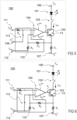
- Figures 5 and 6 illustrate the case wherein the transistor 103 is a NMOS 13
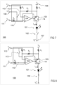
- Figures 7 and 8 illustrate the case wherein the transistor 103 is a PMOS 14.
- the LED 101 comprises an anode connected to the supply voltage terminal T_Vcc 106, a cathode connected to the drain terminal.
- the switch S 102 can be either connected in series between the supply voltage terminal T_Vcc and the anode, or between the cathode and the drain terminal.
- the electrical arrangement 100 further comprises said first resistance R1 which is connected in series with the NMOS.
- said first resistance R1 comprises two resistance terminals, namely T1 R1 and T2 R1 , wherein T1 R1 is connected to the source terminal and wherein T2 R1 is connected to a reference voltage terminal T_V 0 ref , e.g. a ground.
- the secondary electrical arrangement 110 further comprises preferentially a second resistance R2 with resistance terminals T1 R2 and T2 R2 , a third resistance R3 with resistance terminals T1 R3 and T2 R3 , and a fourth resistance R4 with resistance terminals T1 R4 and T2 R4 , wherein the second supply voltage terminal T_Vref 112 is connected to T2 R3 , wherein T1 R3 is connected to T2 R2 and to the negative terminal of the OPA 104, wherein T2 R1 is connected to T1 R1 , and wherein the first supply voltage terminal T_Vin 111 is connected to T1 R4 , and wherein T2 R4 is connected to the positive terminal of the OPA 104.
- the fourth resistance R4 might also be optional, i.e. the first supply voltage terminal T_Vin 111 might be directly connected to the positive terminal of the OPA 104.
- the electrical arrangement 100 is configured for delivering a strictly negative input voltage at the gate terminal when, or at least until, the switch S 102 switches from its OFF state to its ON state, so that the NMOS works as a switch OFF.
- T2 R4 is connected, in addition to the connection to said positive terminal of the OPA, further to said secondary switch NS 113, the latter being configured for connecting, T2 R4 to a reference voltage terminal T_V 1 ref 108 (which might be in particular T_V 0 ref , for instance the ground) when it is in its ON state, and for disconnecting, when it is in its OFF state, T2 R4 from said reference voltage terminal T_V 1 ref 108.
- T_V 1 ref 108 which might be in particular T_V 0 ref , for instance the ground
- the reference voltage terminal T_V 1 ref 108 is configured for delivering a voltage V 1 ref whose value ensures that the voltage difference between the positive and negative terminals of the OPA 104 results in a generation of a current null between the first and second terminals of the transistor 103, in the present case, a NMOS, when the secondary switch NS is ON.
- a pull-down switch that is said secondary switch NS, which works complementary to the switch S 102, is connected to the positive terminal of the OPA 104.
- the positive terminal of the OPA 104 is pulled down and the negative terminal is at a voltage equal to V ref ⁇ R 1 + R 2 R 1 + R 2 + R 3 .
- the NMOS 13 works then in a switch OFF state and the current peak is suppressed.
- the secondary switch NS 113 is connected to T1 R3 and T2 R3 in parallel with the third resistance R3 to pull up the negative terminal to Vref.
- Vref >Vin.
- the PWCS reaches the switch S to turn it ON, the positive terminal of the OPA is at the voltage Vin and the negative terminal of the OPA 104 is pulled up to Vref.
- the NMOS 13 works then in a switch OFF state, suppressing the current peak.
- the secondary switch NS 113 might be configured for connecting T1 R3 to a reference voltage terminal T_V 1 ref .
- the voltage difference between the positive terminal and the negative terminal is kept strictly negative, e.g. at a first voltage value, at least as long as said switch S 102 is in its OFF state, and wherein at the same time as, or at said time T_O1 after, the switch S 102 changes its state from OFF to ON, said voltage difference becomes positive and remains positive, and preferentially equal to a constant value, at least until the switch S 102 switches back from its ON state to its OFF state. Then, at the same time as, or at said time T_O2 after, the switch S 102 switches back its state from the ON state to the OFF state, said voltage difference changes for becoming again strictly negative, and preferentially equal to said first voltage value.
- the MOSFET is a PMOS 14.
- the LED 101 comprises an anode connected to the drain terminal of the PMOS 14, a cathode connected to a reference voltage terminal T_V 0 ref 107, e.g. a ground, wherein said switch S 102 is either connected in series between the reference voltage terminal T_V 0 ref 107 and the cathode, or between the anode and the drain terminal.
- the electrical arrangement 100 further comprises the first resistance R1, connected in series with the PMOS, said first resistance R1 comprising two resistance terminals, namely T1 R1 and T2 R1 , wherein T1 R1 is connected to the source terminal of the PMOS and wherein T2 R1 is connected to a supply voltage terminal T_Vcc 106.
- the secondary electrical arrangement 110 comprises preferentially a second resistance R2 with resistance terminals T1 R2 and T2 R2 , a third resistance R3 with resistance terminals T1 R3 and T2 R3 , and a fourth resistance R4 with resistance terminals T1 R4 and T2 R4 , wherein the second supply voltage terminal T_Vref 112 is connected to T2 R3 , wherein T1 R3 is connected to T2 R2 and to the negative terminal of the OPA 104, wherein T2 R1 is connected to T1 R1 , and wherein the first supply voltage terminal T_Vin 111 is connected to T1 R4 , and wherein T2 R4 is connected to the positive terminal.
- the second supply voltage terminal T_Vref 112 is connected to T2 R3
- T1 R3 is connected to T2 R2 and to the negative terminal of the OPA 104
- T2 R1 is connected to T1 R1
- the first supply voltage terminal T_Vin 111 is connected to T1 R4
- the fourth resistance R4 might also be optional, i.e. the first supply voltage terminal T_Vin 111 might be directly connected to the positive terminal of the OPA 104.
- the gate terminal input voltage is strictly positive when, or at least until, the switch S 102 switches from its OFF state to its ON state so that the PMOS works as a switch OFF.
- T2 R4 is connected, in addition to the connection to said positive terminal, further to said secondary switch NS 113, the latter being configured for connecting, T2 R4 to a reference voltage terminal T_V 1 ref 108 when it is in its ON state, and for disconnecting T2 R4 from said reference voltage terminal T_V 1 ref 108 when it is in its OFF state.
- the reference voltage terminal T_V 1 ref 108 is configured for delivering a voltage V 1 ref whose value ensures that the voltage difference between the positive and negative terminals of the OPA 104 results in a generation of a current null between the first and second terminals of the transistor 103, in the present case, a PMOS, when the secondary switch NS is ON.
- the secondary switch 113 is connected to T1 R3 and T2 R3 in parallel with the third resistance R3.
- the secondary switch NS (113) might be configured for connecting T1 R3 to a reference voltage terminal T_V 1 ref .
- the voltage difference between the positive terminal and negative terminal is kept strictly positive, e.g. at another first voltage value, at least as long as said switch S 102 is in its OFF state. Then, at the same time as, or at said time T_O1 after, the switch S 102 changes its state from OFF to ON, said voltage difference becomes negative and remains negative, and preferentially equal to a constant value, at least until the switch S 102 switches back from its ON state to its OFF state, wherein at the same time as, or at said time T_O2 after, the switch S 102 switches back its state from the ON state to the OFF state, said voltage difference changes for becoming again strictly positive, and preferentially equal to said another first voltage value.
- the present invention proposes an electrical arrangement for driving an LED that comprises a secondary electrical arrangement equipped with a secondary switch NS whose working is correlated to the working of a switch S controlling the activation and deactivation of the LED, wherein said secondary switch enables to control the tension difference applied to the OPA so that any current peak is suppressed when turning ON said LED by means of said switch S.
Landscapes
- Chemical & Material Sciences (AREA)
- Analytical Chemistry (AREA)
- Business, Economics & Management (AREA)
- Emergency Management (AREA)
- Physics & Mathematics (AREA)
- General Physics & Mathematics (AREA)
- Led Devices (AREA)
Abstract
The present invention concerns a method and an electrical arrangement (100) for driving an LED (101), said electrical arrangement (100) comprising:
- said LED (101);
- a switch S (102) connected in series to the LED (101) and configured for controlling a duration of activation of said LED, wherein said switch (102) comprises two states, namely an "ON" state for switching on the LED (101) and an "OFF" state for switching OFF said LED (101);
- a transistor (103);
- an operational amplifier (hereafter "OPA") (104) connected in series to the transistor (103) for controlling a current intensity passing through said LED (101);
the electrical arrangement (100) according to the invention further comprising a secondary electrical arrangement (110) configured for controlling a voltage difference between said positive terminal and said negative terminal in function of said states of the switch S (102) in order to suppress a current peak when turning ON said LED (101).
- said LED (101);
- a switch S (102) connected in series to the LED (101) and configured for controlling a duration of activation of said LED, wherein said switch (102) comprises two states, namely an "ON" state for switching on the LED (101) and an "OFF" state for switching OFF said LED (101);
- a transistor (103);
- an operational amplifier (hereafter "OPA") (104) connected in series to the transistor (103) for controlling a current intensity passing through said LED (101);
the electrical arrangement (100) according to the invention further comprising a secondary electrical arrangement (110) configured for controlling a voltage difference between said positive terminal and said negative terminal in function of said states of the switch S (102) in order to suppress a current peak when turning ON said LED (101).
Description
- The present invention falls within the field of fire detection systems (hereafter "FDS"), and concerns in particular smoke detectors.
- Typically, an optical smoke detector comprises an optical detection chamber equipped with a Light-Emitting Diode (hereafter "LED") and a photoelectric detector positioned in said chamber so as not to receive any direct light from the LED. Indeed, the principle of operation of the optical detector is based on the scattering of the LED light by smoke particles present in said chamber. For example, in case of fire, smoke particles will enter the optical chamber through openings in the walls of the chamber. The light beam emitted by the LED is then configured to interact with these smoke particles so as to diffuse into the optical chamber. The photoelectric detector is configured and positioned to capture at least a portion of this scattered or diffused light, wherein a detection of such scattered light triggers an alarm within the smoke detector or within a fire detection system equipped with said smoke detector.
- One problematic with respect to smoke detectors is related to the aging of the LED. Indeed, with time, the intensity of the light emitted by the LED decreases, which means that the intensity of the scattered light reaching the photoelectric detector will also decrease, falling for instance below an intensity threshold configured for triggering said alarm. This decrease of the intensity of light emitted by the LED is difficult to predict. To avoid any problem related to the aging of the LED, a usual solution consists in replacing periodically the detectors. However, such a solution is not adequate, since it often happens that the LED of the replaced smoke detector is still working perfectly.
- This aging of the LED results notably from the current pulse that is used for powering the smoke detector. The pulsed current provides on one side the advantage of decreasing the energy consumed by the smoke detector, but on the other side, it creates an LED peak current that might be too high (i.e. out of an LED specified range) and uncontrolled with respect to the LED working characteristics. To better illustrate this problematic, a known in the art
LED driver circuit 10 configured for controlling anLED 101 is presented inFig. 1 . A width of said current pulse is controlled by switching between states ON and OFF of aswitch 102, wherein the state ON of saidswitch 102 is configured for connecting in series a cathode of theLED 101 to a drain terminal of aNMOS 13, while the state OFF is configured for disconnecting said LED cathode from said drain terminal, a change from the state OFF to the state ON of saidswitch 102 being controlled by a pulse width control signal (hereafter "PWCS"). The anode of theLED 101 is typically connected to a supply voltage terminal at supply voltage Vcc. TheNMOS 13 is further connected to a first terminal of a first resistance R1 via its source terminal, and, via its gate terminal, to an output terminal of an operational amplifier (hereafter "OPA") 104 which thus controls the gain voltage of theNMOS 13. A current value of said current pulse is then controlled by a voltage signal Vin provided by a digital to analog converter (DAC - not shown) to a positive terminal of theOPA 104, while its negative terminal is connected to said first terminal of the first resistance R1, the other (i.e. second) terminal of said first resistance R1 being typically connected to the ground. The pulse width is usually small (a typical pulse duration (i.e. LED turn-on time) Tp ≤100µs). In particular, the DAC converting and stabilizing time is sometimes non-negligeable with respect to the pulse duration, or even greater than the latter, which may impact the correct working of the LED. - When the switch is in the OFF state, the voltage signal Vin feeds the OPA positive terminal, while its negative terminal is pulled down to the ground. In such a case, the
OPA 104 is in a saturated state with an output voltage Vs up to Vcc (which is, in the example ofFig. 1 , taken as the supply voltage of the OPA) at its output terminal and theNMOS 13 works then as a switch ON. - When the PWCS changes the state of the
switch 102 from the state OFF to the state ON, it generates a current peak which passes through theLED 101. This is notably due to the time required by the OPA 104 to pass from its saturated state at Vcc to a "desaturated state" wherein Vs is effectively controlled by Vin. The current passing through the LED, notably its peak value and its duration, when switching theswitch 102 from its OFF state to its ON state, is not controlled and usually higher than current working ranges defined for the LED. This is one of the main causes of aging (or early aging) of said LED in optical smoke detectors. - It is an objective of the present invention to provide a solution to the previously described LED aging.
- This objective is achieved according to the present invention by a method and an electrical arrangement for driving an LED of a smoke detector according to the object of the independent claims. Dependent claims present further advantages of the invention.
- As explained hereafter, the electrical arrangement and the method according to the invention enable to drive the LED, i.e. to regulate the power to the LED, in a manner free of said current peak that resulted in the early aging of the LED.
- The present invention concerns thus an electrical arrangement for driving an LED, e.g. of an optical smoke detector, said electrical arrangement comprising:
- said LED;
- a switch S, for instance connected in series to the LED, configured for controlling a duration of activation of said LED. Typically, said switch S is configured for connecting said LED to a current path or disconnecting said LED from said current path between a supply voltage Vcc and a reference voltage V0 ref with V0 ref < Vcc. Said switch S comprises two states, namely an "ON" state for switching on the LED (LED activated) and an "OFF" state for switching OFF said LED (LED deactivated). According to the present invention, the change of state of the switch S is preferentially controlled by the PWCS. The latter is for instance sent by a microcontroller or a pulse generator or any appropriate electronic device comprised within the electrical arrangement according to the invention and capable of generating and sending to said switch S a pulsed signal configured for switching ON and OFF the switch S, said pulsed signal comprising preferentially rectangular pulses of width typically smaller or equal to 100µs. Said switch can be any known in the art electrical component capable of connecting (switch ON) or disconnecting (switch OFF) a conducting path between two terminals, wherein the change between the states ON and OFF of said switch is configured for being controlled by said PWCS. It can be an electromechanical switch, or an electronic switch, etc.;
- a transistor comprising a first terminal, a second terminal, and a third terminal. Preferentially, the second terminal is connected in series to the LED. Said transistor is for instance a MOSFET, or a bipolar junction transistor (e.g. a NPN or PNP), or a JFET. Preferentially, said transistor is a MOSFET and the first terminal is a source terminal of said MOSFET, the second terminal is a drain terminal of said MOSFET, and the third terminal is a gate terminal of said MOSFET;
- an operational amplifier (hereafter "OPA") comprising a positive terminal, a negative terminal, and an output terminal connected in series to the third terminal of the transistor for controlling, via said transistor, a current intensity passing through said LED.
- According to the present invention, said electrical arrangement further comprises a secondary electrical arrangement configured for controlling a voltage difference between said positive terminal and said negative terminal in function of said states of the switch S in order to generate a current null between said first terminal and said second terminal before and preferentially at least until, any switching ON of the LED.
- In particular, said control of the voltage difference is configured for generating, at the output terminal of the OPA, in other words, at said third terminal of the transistor, an input voltage V3 (we have V3 = VS with VS being the output voltage at said output terminal of the OPA) configured for generating said current null (i.e. 0A) between said first terminal and said second terminal (i.e. no flow of current between said first terminal and said second terminal), at least as long as said switch S is in its OFF state, and wherein at the same time as, or at a time T_O1 after, the switch S changes its state from OFF to ON, said secondary electrical arrangement is configured for generating, at said third terminal, an input voltage V3' configured for generating a non-zero current between said first terminal and said second terminal (current being therefore allowed to flow between said first terminal and said second terminal) in order to feed the LED at least until the switch S switches back from its ON state to its OFF state, wherein at the same time as, or at a time T_O2 after, the switch S switches back its state from the ON state to the OFF state, said secondary electrical arrangement is configured for generating, at said third terminal, an input voltage V3" configured for generating again said current null between said first terminal and said second terminal, with T_01 and T_02 being both smaller than respectively the time T1 during which the switch S is in its ON state and the time T2 during which the switch S is in its OFF state, and preferentially, V3 = V3".
- The present invention concerns also a method for driving an LED of an optical smoke detector by means of said electrical arrangement comprising the LED, the switch S, the transistor, the OPA, and said secondary electrical arrangement, said method comprising controlling, by means of said secondary electrical arrangement, a voltage difference between said positive terminal and said negative terminal of the OPA in function of said states of the switch S in order to generate a current null between said first terminal and said second terminal before and preferentially at least until, any switching ON of the LED. In particular, said controlling of the voltage difference comprises successively:
- generating, at said third terminal, a third terminal input voltage V3 configured for generating a current null (0A) between said first terminal and said second terminal at least as long as said switch S is in its OFF state;
- at the same time as, or at a time T_O1 after, the switch S changes its state from OFF to ON, generating, by means of said secondary electrical arrangement and at said third terminal, a third terminal input voltage V3' configured for generating a non-zero current between said first terminal and said second terminal in order to feed the LED at least until the switch S switches back from its ON state to its OFF state;
- at the same time as, or at a time T_O2 after, the switch S switches back its state from the ON state to the OFF state, generating, by means of said secondary electrical arrangement, a third terminal input voltage V3" configured for generating again said current null
- Preferentially, the secondary electrical arrangement is configured for connecting a first supply voltage terminal T_Vin to said positive terminal and a second supply voltage terminal T_Vref to the negative terminal and to said first terminal of the transistor. Further, according to a preferred embodiment, the secondary electrical arrangement comprises a secondary switch NS that can switch between an activated state (ON state) and a deactivated state (OFF state), and said control of the voltage difference between said positive terminal and said negative terminal in function of said states of the switch is realized by means of said secondary switch NS, wherein in particular each change of state of the switch S triggers a change of state of the switch NS. Preferentially, the electrical arrangement according to the invention is configured for putting the secondary switch NS in its ON state at least as long as said switch S is in its OFF state, and wherein at the same time as, or at the time T_O1 after, the switch S changes its state from OFF to ON, said secondary switch is configured for changing its state from ON to OFF, remaining in its OFF state at least until the switch S switches back from its ON state to its OFF state, and wherein at the same time as, or at the time T_O2 after, the switch S switches back its state from the ON state to the OFF state, said secondary switch NS is configured for switching its state from the ON state back to the OFF state. Preferentially, said PWCS is configured for also controlling the change of state of the secondary switch NS. In such a case, only the PWCS is effectively generated by the electrical arrangement according to the invention, and used on one hand for controlling the state of the switch S, and, on the other hand, as input to a tertiary electrical arrangement configured for outputting, from said PWCS received as input, an output signal configured for controlling the secondary switch NS. For instance, said tertiary electrical arrangement comprises an inverter, wherein said PWCS passes through said inverter before reaching the secondary switch NS. Alternatively, another PWCS is generated by the electrical arrangement according to the invention and configured for controlling said change of state of the secondary switch NS. Preferentially, the PWCS and said another PWCS are generated and sent by the same electronic device that is capable of generating pulsed signals, e.g. by the same microcontroller or pulse generator of the electrical arrangement according to the invention.
- For a more complete understanding of the present invention, and the advantages thereof, reference is now made to the following description taken in conjunction with the accompanying drawings, wherein like numbers designate like objects, and in which:
-
Figure 1 schematically illustrates an electrical arrangement for driving an LED according to prior techniques; -
Figure 2 schematically illustrates a preferred embodiment of an electrical arrangement for driving an LED according to the invention; -
Figure 3 schematically illustrates a flowchart describing a preferred embodiment of a method according to the invention; -
Figures 4 schematically illustrate a phase delay between the switch S and the secondary switch NS; -
Figures 5 schematically illustrate a first preferred embodiment of a secondary electrical arrangement according to the invention; -
Figure 6 schematically illustrates a second preferred embodiment of a secondary electrical arrangement according to the invention. -
Figure 7 schematically illustrates a third preferred embodiment of a secondary electrical arrangement according to the invention. -
Figure 8 schematically illustrates a fourth preferred embodiment of a secondary electrical arrangement according to the invention. -
FIGURES 1 through 8 , discussed below, and the various embodiments used to describe the principles of the present disclosure in this patent document are by way of illustration only and should not be construed in any way to limit the scope of the disclosure. Those skilled in the art will understand that the principles of the present disclosure may be implemented in any suitably arranged electrical circuit comprising the essential features of the invention. The numerous innovative teachings of the present application will be described with reference to exemplary non-limiting embodiments. - As mentioned in the introduction to the present invention,
Figure 1 describes anelectrical arrangement 10 for driving anLED 101 according to a prior art technique. One technical problem with respect to the electrical arrangement illustrated inFig. 1 is a current peak generated when turning on theLED 101.Figure 2 illustrates a preferred embodiment of anelectrical arrangement 100 for driving anLED 101 according to the invention. Theelectrical arrangement 100 ofFigure 2 solves the above-mentioned problem. Compared toFig. 1 , theelectrical arrangement 100 additionally comprises a secondaryelectrical arrangement 110 configured for controlling a voltage difference between the positive terminal and the negative terminal of theOPA 104 in function of the states, ON, OFF, of aswitch S 102. Through this control, theelectrical arrangement 100 according to the invention is able to suppress said current peak. - More precisely, the
electrical arrangement 100 according to the invention comprises at least: - said
LED 101; - the
switch S 102; - a
transistor 103; - the
OPA 104; and - said secondary
electrical arrangement 110. - The
switch S 102 is connected to theLED 101 for controlling a duration of activation of the latter. As known in the art, when the switch S is in its ON state, the LED is turned ON and emits light. When the switch is in its OFF state, the LED is turned OFF and does not emit light. The state of the switch S is preferentially controlled by the PWCS. As shown inFig. 2 , as well inFig. 5-8 , the switch S is connected to the cathode of theLED 102. However, the skilled person will understand that it might be as well connected to the anode of theLED 102 instead to the cathode. - The
transistor 103 according to the invention might be any known in the art transistor capable of controlling a flow of current configured for feeding the circuit comprising theLED 101 and theswitch S 102, so that said circuit be fed by a current capable of powering the LED during a first period of time, said current being cut off during a second period of time, the successive alternation of said first and second period of times giving rise thus to a periodic feeding of said current to said circuit comprising the LED and the switch S, that is made, as we will explained afterwards, in function the state of the switch S in order to prevent said current peak at the origin of the LED aging. Saidtransistor 103 comprises notably a first terminal, a second terminal, and a third terminal, wherein the third terminal is configured for being connected to anoutput terminal 105 of theOPA 104 that is configured for providing a voltage VS to said third terminal, wherein the second terminal is configured for being connected to said circuit comprising the LED and the switch S connected in series, and the first terminal is preferentially connected to a first resistance R1. In the examples ofFig. 5 and 6 , saidtransistor 103 is aNMOS 13 as inFig. 1 , while inFig. 7 and 8 , said transistor is aPMOS 14. As already pointed out, other types of transistors might of course be used. - The
LED 101, theswitch S 102, thetransistor 103, and preferentially said first resistance R1 are connected in series between a supplyvoltage terminal T_Vcc 106 at supply voltage Vcc and a referencevoltage terminal T_V 0 ref 107 at voltage V0 ref with V0 ref < Vcc. As shown inFig. 5-8 , the order according to which said LED, switch S, transistor, and preferentially or optionally first resistance R1 are connected in series depends notably on the type oftransistor 103 that is used within theelectrical arrangement 100 according to the invention. - The
OPA 104 is configured for outputting a voltage VS at itsoutput terminal 105, wherein said voltage VS is controlled by the secondaryelectrical arrangement 110 according to the invention. As known in the art, theOPA 104 comprises a first OPA power supply terminal powered by a voltage V1 OPA and a second OPA power supply terminal powered by a voltage V2 OPA, with V1 OPA > V2 OPA. Preferentially, the second OPA power supply terminal is connected to the ground, and/or, the first OPA power supply terminal is connected to the supply voltage terminal T_Vcc at supply voltage Vcc, as shown inFig. 1 . - The secondary
electrical arrangement 110 is configured for connecting a first supplyvoltage terminal T_V_in 111 of said electrical arrangement to said positive terminal of theOPA 104, and a second supplyvoltage terminal T_Vref 112 of theelectrical arrangement 100 to the negative terminal of said OPA and as well, and preferentially, to said first terminal of thetransistor 103. The secondaryelectrical arrangement 110 further comprises preferentially asecondary switch NS 113 configured for working essentially in "phase opposition" with theswitch S 102. Said phase opposition is illustrated byFigure 4 and will be described hereafter in more detail. The control of saidsecondary switch NS 113 by the electrical arrangement according to the invention is configured for ensuring that theOPA 104 delivers an output voltage Vs at itsoutput terminal 105 that makes thetransistor 103 generating a current null between its first and second terminals until the LED will be turned ON. This ensures that no current peak is created when turning on the LED. Said control of theswitch NS 113 is realized by means of said PWCS or another PWCS that is correlated to the PWCS or defined in function of the latter. -
Figure 4 shows a comparison between the states ON and OFF of theswitch S 102 and theswitch NS 113 in function of the time. As it can been seen from the graphic, the switches S and NS work essentially in opposition phase, that is each time the switch S passes from the state ON to the state OFF, the switch NS passes from the state OFF to the state ON. This change of state for both switches can be done at the same time or with a delay as illustrated inFig. 4 . Indeed, and preferentially, the switch S and NS are controlled by theelectrical arrangement 100 according to the invention so that when the switch S passes from the state OFF to the state ON at a given time T1, then the switch NS passes from the state ON to the state OFF at a time T1 + T_01. And similarly, when the switch S passes from the state ON to the state OFF at a time T2, then the switch NS passes from the state OFF to the state ON at a time T2 + T_02. Preferentially, T_01 = T_02. In other words, the times T_ON and T_OFF during which the switch S is respectively in its ON state and OFF state are respectively equal to the times TOFF and TON during which the switch NS is respectively in its OFF state and ON state. As illustrated inFig. 4 , T_01 and T_02 are both smaller than respectively the time T_ON during which theswitch S 102 "ON" and the time T_OFF during which theswitch S 102 "OFF". - The concept described above might be generalized to a
transistor 103 driving not only oneLED 101 as shown inFig. 2 , but driving one or several additional LEDs mounted in parallel withLED 101 ofFig. 2 . In other words, thetransistor 103 would be connected to a set of LEDs mounted in parallel, wherein each LED of said set is connected to a respective switch configured for switching ON and OFF the concerned LED. In such a case, the electrical arrangement according to the invention is configured for successively switching ON for a given period of time each LED of said set, so that only one LED is switched ON at a time. In order to implement said successive activation of the LEDs, a microcontroller may generate for each switch in charge of the activation/deactivation of one of the LEDs of the set a PWCS that will activate temporarily "its" LED, wherein the periods of activation of the LEDs are shifted with respect to one another to ensure an activation of a single LED of the set at a time. The secondary electrical arrangement is then configured for controlling the secondary switch NS in function of the PWCS generated for the respective switches of the LEDs so that a current null be generated between the first and second terminal of thetransistor 103 before any switching ON of a LED of said set, letting only current pass between said first and second terminal at the same time as, or at said time T_01 after, the switch of the concerned LED (i.e. configured for activating the concerned LED) be turned ON, as already illustrated inFig. 4 , whose concept applies here mutatis mutandis. - The method according to the invention will be now explained in connection with
Fig. 3 , together withFig. 2 . The description of said method enables to better understand the working principle of theelectrical arrangement 100 according to the invention. In order to drive theLED 101 in a manner free of a generation of a current peak when turning ON said LED, the present method proposes to control the voltage difference between the positive terminal and the negative terminal of the OPA in function of the states of theswitch 102, said control comprising the successive following steps:
Atstep 301, theswitch S 102 is in its OFF state and theLED 101 is therefore turned OFF. At saidstep 301, the secondaryelectrical arrangement 110 is configured for generating, at the third terminal of thetransistor 103, an input voltage V3 configured for making thetransistor 103 generate a current null (0A) between the first terminal and the second terminal at least as long as saidswitch S 102 is in its OFF state. For this purpose, the secondaryelectrical arrangement 110 is configured for maintaining thesecondary switch NS 113 in its ON state at least as long as saidswitch S 102 is in said OFF state. - At
step 302, at the same time as, or at the time T_O1 after, theswitch S 102 changes its state from OFF to ON, the secondaryelectrical arrangement 110 is configured for generating, at said third terminal, an input voltage V3' configured for making thetransistor 103 generate a non-zero current flowing between said first terminal and said second terminal at least until theswitch S 102 switches back from its ON state to its OFF state. For this purpose, the secondary electrical arrangement is configured for automatically switching thesecondary switch 113 from its ON state to its OFF state at said same time as, or at said time T_O1 after, theswitch S 102 changes its state from OFF to ON, and saidsecondary switch 113 being kept in its OFF state by the secondary electrical arrangement at least until theswitch S 102 switches back from its ON state to its OFF state. Preferentially, the PWCS used for switching the state of the switch S from OFF to ON is configured for automatically switching (at said same time or with a time delay equal to T_01) the secondary switch NS from ON to OFF. - At
step 303, at the same time as, or at a time T_O2 after, theswitch S 102 switches back its state from the ON state to the OFF state, the secondaryelectrical arrangement 110 is configured for generating, at said third terminal, an input voltage V3" configured for making the transistor generate again a current null between said first terminal and the second terminal. For this purpose, the secondary electrical arrangement is configured for automatically switching thesecondary switch NS 113 from its OFF state to its ON state at said same time as, or at said time T_O2 after, theswitch S 102 changes its state from ON to OFF, saidsecondary switch NS 113 being kept in its ON state by the secondary electrical arrangement at least until theswitch S 102 switches back again from its OFF state to its ON state, starting the loop again atstep 301. Preferentially, the PWCS used for switching the state of the switch S from ON to OFF is configured for automatically switching (at said same time or with a time delay equal to T_02) the secondary switch NS from OFF to ON. - Preferred embodiments of the secondary
electrical arrangement 110 ofFig. 2 will be illustrated byFig. 5-8 . In the latter, thetransistor 103 is preferentially a MOSFET, wherein the first terminal is a source terminal of said MOSFET, the second terminal is a drain terminal of said MOSFET, and the third terminal is a gate terminal of said MOSFET. In particular,Figures 5 and 6 illustrate the case wherein thetransistor 103 is aNMOS 13, andFigures 7 and 8 illustrate the case wherein thetransistor 103 is aPMOS 14. - According to the
Figures 5 and 6 , theLED 101 comprises an anode connected to the supplyvoltage terminal T_Vcc 106, a cathode connected to the drain terminal. Theswitch S 102 can be either connected in series between the supply voltage terminal T_Vcc and the anode, or between the cathode and the drain terminal. Theelectrical arrangement 100 further comprises said first resistance R1 which is connected in series with the NMOS. Typically, said first resistance R1 comprises two resistance terminals, namely T1R1 and T2R1, wherein T1R1 is connected to the source terminal and wherein T2R1 is connected to a reference voltage terminal T_V0 ref, e.g. a ground. The secondaryelectrical arrangement 110 further comprises preferentially a second resistance R2 with resistance terminals T1R2 and T2R2, a third resistance R3 with resistance terminals T1R3 and T2R3, and a fourth resistance R4 with resistance terminals T1R4 and T2R4, wherein the second supplyvoltage terminal T_Vref 112 is connected to T2R3, wherein T1R3 is connected to T2R2 and to the negative terminal of theOPA 104, wherein T2R1 is connected to T1R1, and wherein the first supplyvoltage terminal T_Vin 111 is connected to T1R4, and wherein T2R4 is connected to the positive terminal of theOPA 104. However, according to the electrical configuration of the secondary electrical arrangement illustrated inFig. 6 , the fourth resistance R4 might also be optional, i.e. the first supplyvoltage terminal T_Vin 111 might be directly connected to the positive terminal of theOPA 104. Theelectrical arrangement 100 is configured for delivering a strictly negative input voltage at the gate terminal when, or at least until, theswitch S 102 switches from its OFF state to its ON state, so that the NMOS works as a switch OFF. - In the preferred embodiment of
Figure 5 , T2R4 is connected, in addition to the connection to said positive terminal of the OPA, further to saidsecondary switch NS 113, the latter being configured for connecting, T2R4 to a reference voltage terminal T_V1 ref 108 (which might be in particular T_V0 ref , for instance the ground) when it is in its ON state, and for disconnecting, when it is in its OFF state, T2R4 from said referencevoltage terminal T_V 1 ref 108. The referencevoltage terminal T_V 1 ref 108 is configured for delivering a voltage V1 ref whose value ensures that the voltage difference between the positive and negative terminals of theOPA 104 results in a generation of a current null between the first and second terminals of thetransistor 103, in the present case, a NMOS, when the secondary switch NS is ON. In other words, according to the preferred embodiment ofFig. 4 , an offset is added on the negative terminal of theOPA 104 with resistance R2, R3, and Vref>Vin. And a pull-down switch, that is said secondary switch NS, which works complementary to theswitch S 102, is connected to the positive terminal of theOPA 104. When the PWCS arrives on the switch S, the positive terminal of theOPA 104 is pulled down and the negative terminal is at a voltage equal to
NMOS 13 works then in a switch OFF state and the current peak is suppressed. - According to
Fig. 6 , thesecondary switch NS 113 is connected to T1R3 and T2R3 in parallel with the third resistance R3 to pull up the negative terminal to Vref. In said case, we have Vref>Vin. When the PWCS reaches the switch S to turn it ON, the positive terminal of the OPA is at the voltage Vin and the negative terminal of theOPA 104 is pulled up to Vref. TheNMOS 13 works then in a switch OFF state, suppressing the current peak. Alternatively, thesecondary switch NS 113 might be configured for connecting T1R3 to a reference voltage terminal T_V1 ref. - According to the embodiments illustrated by
Fig. 5 and 6 , the voltage difference between the positive terminal and the negative terminal is kept strictly negative, e.g. at a first voltage value, at least as long as saidswitch S 102 is in its OFF state, and wherein at the same time as, or at said time T_O1 after, theswitch S 102 changes its state from OFF to ON, said voltage difference becomes positive and remains positive, and preferentially equal to a constant value, at least until theswitch S 102 switches back from its ON state to its OFF state. Then, at the same time as, or at said time T_O2 after, theswitch S 102 switches back its state from the ON state to the OFF state, said voltage difference changes for becoming again strictly negative, and preferentially equal to said first voltage value. -
Figures 7 and 8 apply the same solution to the case of a PMOS. Indeed, in saidFigures 7 and 8 , the MOSFET is aPMOS 14. In this case, theLED 101 comprises an anode connected to the drain terminal of thePMOS 14, a cathode connected to a referencevoltage terminal T_V 0 ref 107, e.g. a ground, wherein saidswitch S 102 is either connected in series between the referencevoltage terminal T_V 0 ref 107 and the cathode, or between the anode and the drain terminal. Theelectrical arrangement 100 further comprises the first resistance R1, connected in series with the PMOS, said first resistance R1 comprising two resistance terminals, namely T1R1 and T2R1, wherein T1R1 is connected to the source terminal of the PMOS and wherein T2R1 is connected to a supplyvoltage terminal T_Vcc 106. The secondaryelectrical arrangement 110 comprises preferentially a second resistance R2 with resistance terminals T1R2 and T2R2, a third resistance R3 with resistance terminals T1R3 and T2R3, and a fourth resistance R4 with resistance terminals T1R4 and T2R4, wherein the second supplyvoltage terminal T_Vref 112 is connected to T2R3, wherein T1R3 is connected to T2R2 and to the negative terminal of theOPA 104, wherein T2R1 is connected to T1R1, and wherein the first supplyvoltage terminal T_Vin 111 is connected to T1R4, and wherein T2R4 is connected to the positive terminal. However, according to the electrical configuration of the secondary electrical arrangement illustrated inFig. 8 , the fourth resistance R4 might also be optional, i.e. the first supplyvoltage terminal T_Vin 111 might be directly connected to the positive terminal of theOPA 104. According to said embodiment, the gate terminal input voltage is strictly positive when, or at least until, theswitch S 102 switches from its OFF state to its ON state so that the PMOS works as a switch OFF. - According to the preferred embodiment of
Fig. 7 , T2R4 is connected, in addition to the connection to said positive terminal, further to saidsecondary switch NS 113, the latter being configured for connecting, T2R4 to a referencevoltage terminal T_V 1 ref 108 when it is in its ON state, and for disconnecting T2R4 from said referencevoltage terminal T_V 1 ref 108 when it is in its OFF state. The referencevoltage terminal T_V 1 ref 108 is configured for delivering a voltage V1 ref whose value ensures that the voltage difference between the positive and negative terminals of theOPA 104 results in a generation of a current null between the first and second terminals of thetransistor 103, in the present case, a PMOS, when the secondary switch NS is ON. According to the alternative preferred embodiment illustrated byFig. 8 , thesecondary switch 113 is connected to T1R3 and T2R3 in parallel with the third resistance R3. Alternatively, the secondary switch NS (113) might be configured for connecting T1R3 to a reference voltage terminal T_V1 ref. - According to the embodiments of
Fig. 7 and 8 , the voltage difference between the positive terminal and negative terminal is kept strictly positive, e.g. at another first voltage value, at least as long as saidswitch S 102 is in its OFF state. Then, at the same time as, or at said time T_O1 after, theswitch S 102 changes its state from OFF to ON, said voltage difference becomes negative and remains negative, and preferentially equal to a constant value, at least until theswitch S 102 switches back from its ON state to its OFF state, wherein at the same time as, or at said time T_O2 after, theswitch S 102 switches back its state from the ON state to the OFF state, said voltage difference changes for becoming again strictly positive, and preferentially equal to said another first voltage value. - The skilled person will understand that in the case of the electrical arrangements described in
Fig. 5 to 8 , the second resistance R2 might be optional, i.e. the describedelectrical arrangement 100 would also work without R2 (e.g. R2 = 0 Ω). - In conclusion, the present invention proposes an electrical arrangement for driving an LED that comprises a secondary electrical arrangement equipped with a secondary switch NS whose working is correlated to the working of a switch S controlling the activation and deactivation of the LED, wherein said secondary switch enables to control the tension difference applied to the OPA so that any current peak is suppressed when turning ON said LED by means of said switch S.
Claims (15)
- An electrical arrangement (100) for driving an LED (101), said electrical arrangement (100) comprising:- said LED (101);- a switch S (102) connected to the LED (101) and configured for controlling a duration of activation of said LED, wherein said switch (102) comprises two states, namely an "ON" state for switching on the LED (101) and an "OFF" state for switching OFF said LED (101);- a transistor (103) comprising a first terminal, a second terminal, and a third terminal;- an operational amplifier, hereafter "OPA", (104) comprising a positive terminal, a negative terminal, and an output terminal connected in series to the third terminal of the transistor (103) for controlling a current intensity passing through said LED (101);the electrical arrangement (100) according to the invention being further characterized in that it comprises:- a secondary electrical arrangement (110) configured for controlling a voltage difference between said positive terminal and said negative terminal in function of said states of the switch S (102) in order to generate a current null between said first terminal and said second terminal before any switching ON of the LED 101.
- Electrical arrangement (100) according to claim 1,
wherein said secondary electrical arrangement (110) is configured for generating, at said third terminal, an input voltage V3 configured for generating said current null between said first terminal and said second terminal at least as long as said switch S (102) is in its OFF state, and wherein at the same time as, or at a time T_01 after, the switch S (102) changes its state from OFF to ON, said secondary electrical arrangement (110) is configured for generating, at said third terminal, an input voltage V3' configured for generating a non-zero current between said first terminal and said second terminal in order to feed the LED at least until the switch S (102) switches back from its ON state to its OFF state, wherein at the same time as, or at a time T_02 after, the switch S (102) switches back its state from the ON state to the OFF state, said secondary electrical arrangement (110) is configured for generating a third terminal input voltage V3" configured for generating again said current null between said first terminal and said second terminal, with T_01 and T_02 being both smaller than respectively the time T_ON during which the switch S (102) is in its ON state and the time T_OFF during which the switch S (102) is in its OFF state. - Electrical arrangement (100) according to claim 1 or 2, wherein said secondary electrical arrangement is configured for connecting a first supply voltage terminal T_V_in (111) to said positive terminal and a second supply voltage terminal T_Vref (112) to the negative terminal and to said first terminal of the transistor (103).
- Electrical arrangement (100) according to one of the claims 1 to 3, wherein said secondary electrical arrangement (110) comprises a secondary switch NS (113), and wherein said control of the voltage difference between said positive terminal and said negative terminal in function of said states of the switch (102) is realized by means of said secondary switch NS(113), wherein each change of state of the switch S (102) triggers a change of state of the switch NS (113).
- Electrical arrangement (100) according to claim 3 and 4, wherein said transistor (103) is a NMOS (13), wherein the first terminal is a source terminal of said NMOS, the second terminal is a drain terminal of said NMOS, and the third terminal is a gate terminal of said NMOS, and wherein the LED (101) comprises an anode connected to a supply voltage terminal T_Vcc (106), a cathode connected to the drain terminal, wherein said switch S (102) is either connected in series between the supply voltage terminal T_Vcc (106) and the anode, or between the cathode and the drain terminal, wherein said electrical arrangement (100) further comprises a first resistance R1 comprising two resistance terminals, namely T1R1 and T2R1, wherein T1R1 is connected to the source terminal and wherein T2R1 is connected to a reference voltage terminal T_V0 ref (107), and wherein the secondary electrical arrangement (110) comprises a second resistance R2 with resistance terminals T1R2 and T2R2, a third resistance R3 with resistance terminals T1R3 and T2R3, and a fourth resistance R4 with resistance terminals T1R4 and T2R4, wherein the second supply voltage terminal T_Vref (112) is connected to T2R3, wherein T1R3 is connected to T2R2 and to the negative terminal, wherein T2R1 is connected to T1R1, and wherein the first supply voltage terminal T_Vin (111) is connected to T1R4, and wherein T2R4 is connected to the positive terminal.
- Electrical arrangement (100) according to claim 5,
wherein T2R4 is connected to said secondary switch NS (113), the latter being configured for connecting T2R4 to a reference voltage terminal T_V1 ref (108) when it is in its ON state, and for disconnecting, when it is in its OFF state, T2R4 from said reference voltage terminal T_V1 ref (107). - Electrical arrangement (100) according to claim 5,
wherein said secondary switch NS (113) is connected to T1R3 and T2R3 in parallel with the third resistance R3, or wherein said secondary switch NS (113) is configured for connecting T1R3 to a reference voltage terminal T_V1 ref. - Electrical arrangement (100) according to one of the claims 5 to 7, configured for keeping said voltage difference between the positive terminal and negative terminal strictly negative at least as long as said switch S (102) is in its OFF state, and wherein at the same time as, or at said time T_O1 after, the switch S (102) changes its state from OFF to ON, said electrical arrangement (100) is configured for making said voltage difference becoming positive and remaining positive at least until the switch S (102) switches back from its ON state to its OFF state, wherein at the same time as, or at said time T_O2 after, the switch S (102) switches back its state from the ON state to the OFF state, said electrical arrangement (100) is configured for changing said voltage difference to make it again strictly negative.
- Electrical arrangement (100) according to claims 3 and 4, wherein said transistor (103) is a PMOS (14), wherein the first terminal is a source terminal of said PMOS, the second terminal is a drain terminal of said PMOS, and the third terminal is a gate terminal of said PMOS, the LED (101) comprising an anode connected to the drain terminal, a cathode connected to a reference voltage terminal T_V0 ref (107), wherein said switch S (102) is either connected in series between the reference voltage terminal T_V0 ref (107) and the cathode, or between the anode and the drain terminal, wherein said electrical arrangement (100) further comprises a first resistance R1 comprising two resistance terminals, namely T1R1 and T2R1, wherein T1R1 is connected to the source terminal and wherein T2R1 is connected to a supply voltage terminal T_Vcc (106), and wherein the secondary electrical arrangement (110) comprises a second resistance R2 with resistance terminals T1R2 and T2R2, a third resistance R3 with resistance terminals T1R3 and T2R3, and a fourth resistance R4 with resistance terminals T1R4 and T2R4, wherein the second supply voltage terminal T_Vref is connected to T2R3, wherein T1R3 is connected to T2R2 and to the negative terminal, wherein T2R1 is connected to T1R1, and wherein the first supply voltage terminal T_Vin (111) is connected to T1R4, and wherein T2R4 is connected to the positive terminal of the OPA (104).
- Electrical arrangement (100) according to claim 9,
wherein T2R4 is connected to said secondary switch NS (113), the latter being configured for connecting T2R4 to a reference voltage terminal T_V1 ref (108) when it is in its ON state, and for disconnecting T2R4 from said reference voltage terminal T_V1 ref (108) when it is in its OFF state. - Electrical arrangement (100) according to claim 9,
wherein said secondary switch NS (113) is connected to T1R3 and T2R3 in parallel with the third resistance R3, or wherein said secondary switch NS (113) is configured for connecting T1R3 to a reference voltage terminal T_V1 ref. - Electrical arrangement (100) according to one of the claims 9 to 11, configured for keeping said voltage difference between the positive terminal and negative terminal strictly positive at least as long as said switch S (102) is in its OFF state, and wherein at the same time as, or at said time T_O1 after, the switch S (102) changes its state from OFF to ON, said electrical arrangement (100) is configured for making said voltage difference becoming negative and remaining negative at least until the switch S (102) switches back from its ON state to its OFF state, wherein at the same time as, or at said time T_O2 after, the switch S (102) switches back its state from the ON state to the OFF state, said electrical arrangement (100) is configured for changing said voltage difference to make it again strictly positive.
- A method for driving an LED (101) of an optical smoke detector by means of an electrical arrangement (100), said electrical arrangement comprising:- said LED (101);- a switch S (102) connected in series to the LED (101) and configured for controlling a duration of activation of said LED, wherein said switch (102) comprises two states, namely an "ON" state for switching on the LED (101) and an "OFF" state for switching OFF said LED (101);- a transistor (103) comprising a first terminal, a second terminal, and a third terminal;- an operational amplifier, hereafter "OPA", (104) comprising a positive terminal, a negative terminal, and an output terminal connected in series to the third terminal of the transistor (103) for controlling a current intensity passing through said LED (101);said method comprising the following steps:- controlling, by means of a secondary electrical arrangement (110) of said electrical arrangement (100), a voltage difference between said positive terminal and said negative terminal in function of said states of the switch S (102) in order to generate a current null between said first terminal and said second terminal before any switching ON of the LED 101.
- The method according to claim 13, wherein said controlling comprises successively the following steps:- generating (301), at said third terminal, an input voltage V3 configured for generating a current null between said first terminal and said second terminal at least as long as said switch S (102) is in its OFF state;- at the same time as, or at a time T_O1 after, the switch S (102) changes its state from OFF to ON, generating (302), by means of said secondary electrical arrangement (110) and at said third terminal, an input voltage V3' configured for generating a non-zero current between said first terminal and said second terminal in order to feed the LED at least until the switch S (102) switches back from its ON state to its OFF state;- at the same time as, or at a time T_O2 after, the switch S (102) switches back its state from the ON state to the OFF state, generating (303), by means of said secondary electrical arrangement (110), an input voltage V3" configured for generating again said current null between said first terminal and said second terminal;wherein T_01 and T_02 are both smaller than respectively the time T_ON during which the switch S (102) is in its ON state and the time T_OFF during which the switch S (102) is in its OFF state.
- The method according to claim 13 or 14, wherein the secondary electrical arrangement (110) comprises a secondary switch NS (113), and wherein said controlling of the voltage difference between said positive terminal and said negative terminal in function of said states of the switch (102) comprises:- keeping said secondary switch NS (113) in its ON state at least as long as said switch S (102) is in its OFF state;- at the same time as, or at the time T_O1 after, the switch S (102) changes its state from OFF to ON, changing the state of said secondary switch NS (113) from its ON state to its OFF state, and keeping said secondary switch NS (113) in its OFF state at least until the switch S (102) switches back from its ON state to its OFF state; and- at the same time as, or at the time T_O2 after, the switch S (102) switches back its state from the ON state to the OFF state, switching the state of said secondary switch NS (113) from its ON state back to its OFF state.
Priority Applications (1)
| Application Number | Priority Date | Filing Date | Title |
|---|---|---|---|
| EP23178865.4A EP4478837A1 (en) | 2023-06-13 | 2023-06-13 | System and method for suppressing an led current peak |
Applications Claiming Priority (1)
| Application Number | Priority Date | Filing Date | Title |
|---|---|---|---|
| EP23178865.4A EP4478837A1 (en) | 2023-06-13 | 2023-06-13 | System and method for suppressing an led current peak |
Publications (1)
| Publication Number | Publication Date |
|---|---|
| EP4478837A1 true EP4478837A1 (en) | 2024-12-18 |
Family
ID=86764427
Family Applications (1)
| Application Number | Title | Priority Date | Filing Date |
|---|---|---|---|
| EP23178865.4A Pending EP4478837A1 (en) | 2023-06-13 | 2023-06-13 | System and method for suppressing an led current peak |
Country Status (1)
| Country | Link |
|---|---|
| EP (1) | EP4478837A1 (en) |
Citations (2)
| Publication number | Priority date | Publication date | Assignee | Title |
|---|---|---|---|---|
| CN206640829U (en) * | 2017-02-10 | 2017-11-14 | 深圳欧创芯半导体有限公司 | Low voltage difference output current overshoot suppression circuit |
| CN112333883A (en) * | 2020-11-02 | 2021-02-05 | 无锡职业技术学院 | PWM Dimmable LED Lighting System to Avoid Inductor Current Overshoot |
-
2023
- 2023-06-13 EP EP23178865.4A patent/EP4478837A1/en active Pending
Patent Citations (2)
| Publication number | Priority date | Publication date | Assignee | Title |
|---|---|---|---|---|
| CN206640829U (en) * | 2017-02-10 | 2017-11-14 | 深圳欧创芯半导体有限公司 | Low voltage difference output current overshoot suppression circuit |
| CN112333883A (en) * | 2020-11-02 | 2021-02-05 | 无锡职业技术学院 | PWM Dimmable LED Lighting System to Avoid Inductor Current Overshoot |
Similar Documents
| Publication | Publication Date | Title |
|---|---|---|
| US8339046B2 (en) | Lighting control device of lighting device for vehicle | |
| US7746300B2 (en) | Circuit and methodology for supplying pulsed current to a load, such as a light emitting diode | |
| US7991032B2 (en) | Laser drive | |
| US20110291634A1 (en) | Overcurrent protection circuit and overcurrent protection method | |
| EP2367273A2 (en) | Power control system startup method and circuit | |
| JP6295268B2 (en) | Semiconductor drive device | |
| US3887836A (en) | Optical driver circuit | |
| JP2009189206A (en) | Inrush current prevention circuit | |
| US12155174B2 (en) | Drive circuit | |
| US20080315688A1 (en) | Pulsed power supply | |
| US11482836B2 (en) | Laser diode driver circuits and methods of operating thereof | |
| US11522535B2 (en) | Semiconductor device | |
| KR20070001201A (en) | Laser element drive device | |
| US7368885B2 (en) | Lighting controller for lighting device for vehicle | |
| JP3595532B2 (en) | Drive control device for semiconductor laser | |
| KR20180057600A (en) | Led emitting device and driving method thereof | |
| EP1404014B1 (en) | Power circuit | |
| JPH098631A (en) | LED drive circuit | |
| US20230098998A1 (en) | Drive circuit and light source device | |
| KR20050037915A (en) | Circuit of optic sensor | |
| US10111287B2 (en) | Synchronous switching circuit | |
| US20240322822A1 (en) | Semiconductor device | |
| US10761470B2 (en) | Printing apparatus and light-emitting element driving device | |
| US10660169B1 (en) | Digital standby control of a lighting driver using peak detection of pulse width modulated output reference control signal | |
| JP2024057628A (en) | Inrush current prevention circuit |
Legal Events
| Date | Code | Title | Description |
|---|---|---|---|
| PUAI | Public reference made under article 153(3) epc to a published international application that has entered the european phase |
Free format text: ORIGINAL CODE: 0009012 |
|
| STAA | Information on the status of an ep patent application or granted ep patent |
Free format text: STATUS: THE APPLICATION HAS BEEN PUBLISHED |
|
| AK | Designated contracting states |
Kind code of ref document: A1 Designated state(s): AL AT BE BG CH CY CZ DE DK EE ES FI FR GB GR HR HU IE IS IT LI LT LU LV MC ME MK MT NL NO PL PT RO RS SE SI SK SM TR |
|
| STAA | Information on the status of an ep patent application or granted ep patent |
Free format text: STATUS: REQUEST FOR EXAMINATION WAS MADE |
|
| 17P | Request for examination filed |
Effective date: 20250603 |