EP4478721A1 - Display device - Google Patents
Display device Download PDFInfo
- Publication number
- EP4478721A1 EP4478721A1 EP23824029.5A EP23824029A EP4478721A1 EP 4478721 A1 EP4478721 A1 EP 4478721A1 EP 23824029 A EP23824029 A EP 23824029A EP 4478721 A1 EP4478721 A1 EP 4478721A1
- Authority
- EP
- European Patent Office
- Prior art keywords
- pcb
- display device
- antenna
- frame
- antenna portion
- Prior art date
- Legal status (The legal status is an assumption and is not a legal conclusion. Google has not performed a legal analysis and makes no representation as to the accuracy of the status listed.)
- Pending
Links
Images







Classifications
-
- H—ELECTRICITY
- H01—ELECTRIC ELEMENTS
- H01Q—ANTENNAS, i.e. RADIO AERIALS
- H01Q21/00—Antenna arrays or systems
- H01Q21/28—Combinations of substantially independent non-interacting antenna units or systems
-
- H—ELECTRICITY
- H01—ELECTRIC ELEMENTS
- H01Q—ANTENNAS, i.e. RADIO AERIALS
- H01Q1/00—Details of, or arrangements associated with, antennas
- H01Q1/02—Arrangements for de-icing; Arrangements for drying-out ; Arrangements for cooling; Arrangements for preventing corrosion
-
- H—ELECTRICITY
- H01—ELECTRIC ELEMENTS
- H01Q—ANTENNAS, i.e. RADIO AERIALS
- H01Q1/00—Details of, or arrangements associated with, antennas
- H01Q1/12—Supports; Mounting means
- H01Q1/1207—Supports; Mounting means for fastening a rigid aerial element
-
- H—ELECTRICITY
- H01—ELECTRIC ELEMENTS
- H01Q—ANTENNAS, i.e. RADIO AERIALS
- H01Q1/00—Details of, or arrangements associated with, antennas
- H01Q1/12—Supports; Mounting means
- H01Q1/22—Supports; Mounting means by structural association with other equipment or articles
-
- H—ELECTRICITY
- H01—ELECTRIC ELEMENTS
- H01Q—ANTENNAS, i.e. RADIO AERIALS
- H01Q1/00—Details of, or arrangements associated with, antennas
- H01Q1/12—Supports; Mounting means
- H01Q1/22—Supports; Mounting means by structural association with other equipment or articles
- H01Q1/2283—Supports; Mounting means by structural association with other equipment or articles mounted in or on the surface of a semiconductor substrate as a chip-type antenna or integrated with other components into an IC package
-
- H—ELECTRICITY
- H01—ELECTRIC ELEMENTS
- H01Q—ANTENNAS, i.e. RADIO AERIALS
- H01Q1/00—Details of, or arrangements associated with, antennas
- H01Q1/12—Supports; Mounting means
- H01Q1/22—Supports; Mounting means by structural association with other equipment or articles
- H01Q1/24—Supports; Mounting means by structural association with other equipment or articles with receiving set
-
- H—ELECTRICITY
- H01—ELECTRIC ELEMENTS
- H01Q—ANTENNAS, i.e. RADIO AERIALS
- H01Q1/00—Details of, or arrangements associated with, antennas
- H01Q1/52—Means for reducing coupling between antennas; Means for reducing coupling between an antenna and another structure
- H01Q1/526—Electromagnetic shields
-
- H—ELECTRICITY
- H01—ELECTRIC ELEMENTS
- H01Q—ANTENNAS, i.e. RADIO AERIALS
- H01Q21/00—Antenna arrays or systems
- H01Q21/06—Arrays of individually energised antenna units similarly polarised and spaced apart
- H01Q21/08—Arrays of individually energised antenna units similarly polarised and spaced apart the units being spaced along or adjacent to a rectilinear path
-
- H—ELECTRICITY
- H04—ELECTRIC COMMUNICATION TECHNIQUE
- H04N—PICTORIAL COMMUNICATION, e.g. TELEVISION
- H04N5/00—Details of television systems
- H04N5/64—Constructional details of receivers, e.g. cabinets or dust covers
-
- H—ELECTRICITY
- H05—ELECTRIC TECHNIQUES NOT OTHERWISE PROVIDED FOR
- H05K—PRINTED CIRCUITS; CASINGS OR CONSTRUCTIONAL DETAILS OF ELECTRIC APPARATUS; MANUFACTURE OF ASSEMBLAGES OF ELECTRICAL COMPONENTS
- H05K7/00—Constructional details common to different types of electric apparatus
- H05K7/20—Modifications to facilitate cooling, ventilating, or heating
- H05K7/20954—Modifications to facilitate cooling, ventilating, or heating for display panels
-
- H—ELECTRICITY
- H01—ELECTRIC ELEMENTS
- H01Q—ANTENNAS, i.e. RADIO AERIALS
- H01Q21/00—Antenna arrays or systems
- H01Q21/24—Combinations of antenna units polarised in different directions for transmitting or receiving circularly and elliptically polarised waves or waves linearly polarised in any direction
-
- H—ELECTRICITY
- H01—ELECTRIC ELEMENTS
- H01Q—ANTENNAS, i.e. RADIO AERIALS
- H01Q9/00—Electrically-short antennas having dimensions not more than twice the operating wavelength and consisting of conductive active radiating elements
- H01Q9/04—Resonant antennas
- H01Q9/0407—Substantially flat resonant element parallel to ground plane, e.g. patch antenna
-
- H—ELECTRICITY
- H01—ELECTRIC ELEMENTS
- H01Q—ANTENNAS, i.e. RADIO AERIALS
- H01Q9/00—Electrically-short antennas having dimensions not more than twice the operating wavelength and consisting of conductive active radiating elements
- H01Q9/04—Resonant antennas
- H01Q9/16—Resonant antennas with feed intermediate between the extremities of the antenna, e.g. centre-fed dipole
Definitions
- the present disclosure relates to a display device.
- LCDs Liquid Crystal Displays
- OLED Organic Light-Emitting Diode
- micro-LED displays have been recently researched and used.
- an LCD panel includes a TFT substrate and a color substrate, which face each other with a liquid crystal layer interposed therebetween, in order to display an image using light supplied from a backlight unit.
- an OLED panel is configured to display an image by depositing a self-luminescent organic layer on a substrate having a transparent electrode formed thereon. Particularly, because a display device including an OLED panel do not need a backlight unit, there is an advantage of being capable of realizing an ultraslim display device.
- a control box may be spaced apart from a display device, and may be used in the state of being close to a user.
- the control box may provide the display device with a variety of information.
- the control box may be an AV box.
- the control box may transmit and receive information to and from a display head equipped with a display panel configured to display an image with or without wires.
- a display device may include a display panel, a frame positioned behind the display panel and coupled to the display panel, and a communication box disposed adjacent one side of the frame and coupled to the frame, wherein the communication box may include an inner plate which extends in a vertical direction of the display panel, and an antenna module which defines a flat surface in a direction which intersects the vertical direction of the display panel and is fixed to the inner plate.
- a display device including a wireless communication module.
- a display device capable of improving reception efficiency of an antenna of a communication module.
- FIGS. 1 to 15 are views illustrating display devices according to embodiments of the present disclosure.
- suffixes such as “module” and “unit” may be used to refer to elements or components.
- the use of such suffixes herein is merely intended to facilitate description of the specification, and the suffixes do not have any special meaning or function.
- a display device 1 may include a display panel 10.
- the display panel 10 may display a screen.
- the display device 1 may include a first long side LS1, a second long side LS2 opposed to the first long side LS1, a first short side SS1 adjacent to the first long side LS1 and the second long side LS2, and a second short side SS2 opposed to the first short side SS1.
- first and second long sides LS1 and LS2 is illustrated and described as being longer than each of the first and second short sides SS1 and SS2 for convenience of explanation, the length of each of the first and second long sides LS1 and LS2 may be almost equal to that of each of the first and second short sides SS1 and SS2.
- a direction parallel to the long sides LS1 and LS2 of the display device 1 may be referred to as a lateral direction or a first direction DR1.
- a direction parallel to the short sides SS1 and SS2 of the display device 1 may be referred to as a vertical direction or a second direction DR2.
- a direction perpendicular to the long sides LS1 and LS2 and the short sides SS1 and SS2 of the display device 1 may be referred to as a forward/backward direction or a third direction DR3.
- a direction in which the display panel 10 displays an image may be referred to as a forward direction F, and the opposite direction may be referred to as a rearward direction R.
- the first long side LS1 may be referred to as an upper side U or y.
- the second long side LS2 may be referred to as a lower side D.
- the first short side SS1 may be referred to as a left side Le or x.
- the second short side SS2 may be referred to as a right side Ri.
- the first long side LS1, the second long side LS2, the first short side SS1, and the second short side SS2 may be collectively referred to as an edge of the display device 1. Furthermore, the points at which the first long side LS1, the second long side LS2, the first short side SS1, and the second short side SS2 meet each other may be referred to as corners.
- first corner C1 the point at which the first short side SS1 and the first long side LS1 meet each other may be referred to as a first corner C1.
- first longs side LS1 and the second short side SS2 meet each other may be referred to as a second corner C2.
- second corner C2 The point at which the second short side SS2 and the second long side LS2 meet each other may be referred to as a third corner C3.
- the display device 1 may include the display panel 10, a frame 20, a side frame 30, and a back cover 40.
- the display panel 10 may define the front surface of the display device 1, and may display an image on the front surface of the display device 1.
- the display panel 10 may be an OLED (Organic Light-Emitting Diode) panel.
- OLED Organic Light-Emitting Diode
- a display panel applicable to the present disclosure is not limited to the OLED panel.
- the display panel 10 may divide an image into a plurality of pixels, and may control the color, brightness and chroma of each of the pixels, thereby outputting the image.
- the display panel 10 may be divided into an active area, in which an image is displayed, and an inactive area, in which an image is not displayed.
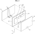
- the display panel 10 may generate light corresponding to red, green or blue in response to a control signal.
- the frame 20 may be positioned behind the display panel 10, and the display panel 10 may be coupled to the frame 20.
- the frame 20 may include a metal material.
- the frame 20 may be referred to a main frame or a module cover.
- the side frame 30 may extend along the periphery of the frame 20.
- the frame 20 may be coupled to the side frame 30 from the front of the side frame 30.
- the side frame 30 may cover the lateral side surfaces of the display panel 10 and the frame 20.
- the side frame 30 may be referred to as a guide panel.
- the back cover 40 may be positioned behind the frame 20, and may be coupled to the frame 20.
- the back cover 40 may be injection-molded from a resin material.
- the back cover 40 may include a metal material.
- boards 50 may be mounted to the frame 20 from the rear of the frame 20.
- a plurality of electronic elements may be mounted on the boards 50.
- the boards 50 may be PCBs (Printed Circuit Boards), and may be electrically connected to electronic parts of the display device.
- the boards 50 may include a power supply board 51 configured to supply power to the individual components of the display device, a timing controller board 52 configured to provide an image signal to the display panel 10, and a main board 53 configured to provide an image signal to the display panel 10 and/or the timing controller board 52 and to control the display device.
- a power supply board 51 configured to supply power to the individual components of the display device
- a timing controller board 52 configured to provide an image signal to the display panel 10
- a main board 53 configured to provide an image signal to the display panel 10 and/or the timing controller board 52 and to control the display device.
- an S-PCB 11 (Source PCB, see FIG. 2 ) may be adjacent to the lower side of the display panel 10, and may be coupled to the rear surface of the display panel 10.
- a cable C may extend through a cable hole CH formed in the lower portion of the frame 20, and may connect the S-PCB 11 to the timing controller board 52. Accordingly, the cable C may transmit digital video data and a timing control signal to the S-PCB 11 from the timing controller board 52.
- the cable C may be an FFC (Flexible Flat Cable) .
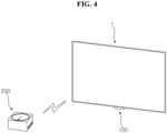
- a control box 200 may be spaced apart from the display device 1.
- the control box 200 may be referred to as a set-top box.
- the control box 200 may transmit and receive information to and from the display device 1 without wires.
- the communication module (not shown) of the control box 200 may perform wireless communication with the communication module 100 of the display device 1. At least a portion of the communication module 100 may project to the outside from the edge of the display device 1. Accordingly, the communication module 100 may perform efficient wireless communication with the communication module of the control box 200.
- Stability of wireless communication between the control box 200 and the display device 1 may be dependent on the relative position between the control box 200 and the display device 1.
- the display device 1 may be positioned at a constant location in order to maintain a certain distance to a user. There is a need to allow the control box 200 to be freely positioned for user convenience.
- control box 200 may be one component of the display device 1.
- the display device 1 including the display panel 10 may be referred to as a head 1.
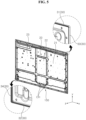
- the side frame 30 may include a first part 31, a second part 32, a third part 33, and a fourth part 34.
- the first part 31 may extend along the upper side of the frame 20, and may define the first long side LS1 (see FIG. 1 ).
- the third part 33 may be bent downwards at the right end of the first part 1 and may then extend along the right side of the frame 20, thereby defining the second short side SS2 (see FIG. 1 ).
- the second part 32 may be bent at the lower end of the third part 33 and may then extend along the lower side of the frame 20, thereby defining the second long side LS2 (see FIG. 1 ).
- the fourth part 34 may be bent upwards at the end of the second part 32 and may then extend along the left side of the frame 20, thereby defining the first short side SS1 (see FIG. 1 ).
- a first forming portion 21, a second forming portion 22, and a third forming portion 23 may be formed by pressing the front surface of the frame 20 rearwards.
- the first forming portion 21 may be positioned close to the right side of the frame 20, the third forming portion 23 may be positioned close to the left side of the frame 20, and the second forming portion 22 may be positioned between the first forming portion 21 and the third forming portion 23.
- the power supply board 51 (see FIG. 3 ) may be mounted on the rear surface of the first forming portion 21.
- the timing controller board 52 (see FIG. 3 ) may be mounted on the rear surface of the second forming portion 22.
- the main board 53 (see FIG. 3 ) may be mounted on the rear surface of the third forming portion 23.
- a shield plate 520 may be mounted on the rear surface of the timing controller board 52.
- a first board 54 may be spaced apart downwards from the timing controller board 52, and may be mounted on the rear surface of the frame 20.
- a second board 53 may be spaced rightwards apart from the timing controller board 52, and may be mounted on the rear surface of the frame 20.
- the shield plate (not shown) may be mounted on the rear surfaces of the first board 54 and the second board 53.
- the communication module 100 may receive compressed sound and/or video data from the communication module of the control box 200 (see FIG. 4 ).
- the first board 54 may release and convert the compressed sound and/or video data received from the communication module 100 and may provide the converted data to the second board 53.
- the second board 53 may provide the data received from the first board 54 to the display panel 10 (see FIG. 3 ) through the timing controller board 52.
- the first board 54 may be WAV (waveform audio format) board or a WAV22 board
- the second board 53 may be an AMP (amplifier) board.
- the second board 53 may be the main board 53.
- the communication module 100 may be referred to as a communication unit 100 or a communication box 100.
- a first cable hole CH1 and a second cable hole CH2 may be formed through the frame 20 in the forward/backward direction, and may be adjacent to the second part 32.
- the first cable hole CH1 may be close to the second cable hole CH2 but be spaced apart from the second cable hole CH2.
- the four cables C may constitute two pairs of cables. One pair of cables may extend through the first cable hole CH1, and the other pair of cables may extend through the second cable hole CH2.
- the second part 32 may include a vertical portion 32V and a horizontal portion 32H.
- the vertical portion 32V may extend along the lower side of the frame 20, and may define the lower side of the second part 32.
- the vertical portion 32V may have a width in a direction in which the vertical portion 32V intersects the frame 20. In other words, the length of the vertical portion 32V may be defined in the lateral direction, and the width of the vertical portion 32V may be defined in the forward/backward direction.
- the thickness of the vertical portion 32V may be defined in the vertical direction.
- the horizontal portion 32H may project toward the rear of the frame 20 from the upper side of the frame 20.
- the horizontal portion 32H may be disposed behind the frame 20 so as to be parallel to the frame 20.
- the length of the horizontal portion 32H may be defined in the lateral direction
- the width of the horizontal portion 32H may be defined in the vertical direction.
- the thickness of the horizontal portion 32H may be defined in the forward/backward direction.
- a pressed portion 25 may be formed by pressing the rear surface of the frame 20 forwards, and may define the lower side of the frame 20.
- the front surface of the pressed portion 25 may be in contact with the rear surface of the horizontal portion 32H.
- the horizontal portion 32H may be coupled or fixed to the pressed portion 25.
- Lower fixing portions 26a and 26b may project toward the horizontal portion 32H from the pressed portion 25, and may extend through the horizontal portion 32H.
- a first lower fixing portion 26a may be spaced leftwards apart from a second lower fixing portion 26b.
- Upper fixing portions 24a and 24b may project rearwards from the frame 20.
- a first upper fixing portion 24a may be adjacent to the first cable hole CH1, and a second upper fixing portion 24b may be adjacent to the second cable hole CH2.
- the lower fixing portions 26a and 26b and the upper fixing portions 24a and 24b may be PEM nuts.
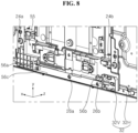
- a base 55 may be removably coupled to the frame 20 and the second part 32 at the rear of the frame 20.
- the base 55 may be positioned above the vertical portion 32V.
- a portion of the base 55 may cover at least a portion of the rear surface of the cable holes CH1 and CH2 (see FIG. 7 ).
- a portion of the base 55 may cover a portion of the rear surface of the horizontal portion 32H.
- the lower fixing portions 26a and 26b and the upper fixing portions 24a and 24b may extend through the base 55.
- Bosses 56a and 56b and a third lower fixing portion 56c may project rearwards from the base 55.
- the third lower fixing portion 56c may be adjacent to the vertical portion 32V, and may be opposed to the horizontal portion 32H based on the base 55.
- the third lower fixing portion 56c may be opposed to the second lower fixing portion 26b based on the first lower fixing portion 26a.
- a first boss 56a may be adjacent to the third lower fixing portion 56c, and may be spaced upwards apart from the third lower fixing portion 56c.
- a second boss 56b may be adjacent to the second lower fixing portion 26b, and may be spaced upwards apart from the second lower fixing portion 26b.
- the third lower fixing portion 56c may be a PEM nut. Meanwhile, bosses 56a and 56b may be referred to as fixing pins.
- the communication module 100 may include a rear cover 100a, a front cover 100b, an inner plate 120, a first antenna module 130, a second antenna module 140, and an infrared transmitting and receiving unit 150.
- the antenna modules 130 and 140 may be referred to as antennas 130 and 140.
- the inner plate 120 may be coupled or fixed to the front surface of the rear cover 110a.
- the rear cover 110a may be made of plastic through injection molding.
- the inner plate 120 may be referred to as a radiation plate 120.
- the inner plate 120 may include metal.
- the inner plate 120 may include aluminum.
- the inner plate 120 may include a central plate 121, a first connecting plate 122, and a second connecting plate 123.
- the first connecting plate 122 may be opposed to the second connecting plate 123 based on the central plate 121.
- the infrared transmitting and receiving unit 150 may be positioned between the first connecting plate 122 and the second connecting plate 123, and may be coupled or fixed to the rear cover 110a.
- the infrared transmitting and receiving unit 150 may be positioned below the central plate 121.
- the first antenna 130 may be coupled or fixed to the first connecting plate 122, and the second antenna 140 may be coupled or fixed to the second connecting plate 123.
- the first antenna 130 may be a left-side antenna
- the second antenna 140 may be a right-hand antenna.
- the front cover 110b may be coupled to the rear cover 110a.
- the front cover 110b may cover the first antenna 130, the second antenna 140 and/or the infrared transmitting and receiving unit 150.
- the front cover 110b may be made of plastic through injection molding.
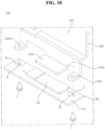
- the first connecting plate 122 may include a body portion 122a, a first leg 122b, and an extension plate 122c.
- the first leg 122b may extend from one side of the body portion 122a, and may be bent at the end thereof.
- the second leg 122d may extend from the other side of the body portion 122a, and may be bent at the end thereof.
- the extension plate 122c may be positioned between the first leg 122b and the second leg 122d, and may extend from the body portion 122a and be bent.
- the extension plate 122c may extend from the body portion 122a and be bent.
- the first antenna module 130 may include a board 131 and a shield cover 132.
- the board 131 may include a front surface and a rear surface. Electronic elements may be mounted on the rear surface of the board 131.
- the shield cover 132 may be coupled to the rear surface of the board 131 so as to cover the electronic elements.
- the shield cover 132 may be a conductor.
- the shield cover 132 may include metal. Holes H may be formed in two opposite sides of the board 131.
- the board 131 may be coupled to the bent ends of the first leg 122b and/or the second leg 122d by means of fastening members f.
- An electrode EL may be formed on the rear surface of the board 131 so as to correspond to the first leg 122b and/or the second leg 122d.
- Each of the first leg 122b and/or the second leg 122d may be in contact with the electrode EL, and the electrode EL may be electrically connected to the first leg 122b and/or the second leg 122d.
- the legs 122b and 122d may be conductors. Current leaking from the board 131 may be grounded via the electrode EL and the legs 122b and 122d. Furthermore, the heat generated by the board 131 may be transmitted via the legs 122b and 122d.
- the extension plate 122c may be bent so as to face the rear surface of the board 131, and may be in contact with the shield cover 132.
- the extension plate 122c may be a conductor.
- the heat generated by the first antenna module 130 may be transmitted via the shield cover 132 and the extension plate 122c.
- the current leaking from the first antenna module 130 may be grounded via the shield cover 132 and the extension plate 122c.
- the front surface of the first antenna module 130 may face downwards.
- the front surface and/or the rear surface of the board 131 of the first antenna module 130 may be perpendicular to the front surface of the display panel 10.
- the second connecting plate 123 may include a body portion 123a, a first leg 123b, a second leg 123d, and an extension plate 123c.
- the first leg 123b may extend from one side of the body portion 123a, and may be bent at the end thereof.
- the second leg 123d may extend from the other side of the body portion 123a, and may be bent at the end thereof.
- the extension plate 123c may be positioned between the first leg 123b and the second leg 123d, and may extend from the body portion 123a and be bent.
- the extension plate 123c may extend from the body portion 123a and may be bent.
- the second antenna module 140 may include a board 141 and a shield cover 142.
- the board 141 may include a front surface and a rear surface. Electronic elements may be mounted on the rear surface of the boad 141.
- the shield cover 142 may be coupled to the rear surface of the board 141 so as to cover the electronic elements.
- the shield cover 142 may be a conductor.
- the shield cover 142 may include metal.
- the board 141 may be coupled to the bent ends of the first leg 123b and/or the second leg 123d by means of fastening members f.
- the electrode EL (see FIG. 10 ) may be formed on the rear surface of the board 141 so as to correspond to the first leg 123b and/or the second leg 123d.
- Each of the first leg 123b and/or the second leg 123d may be in contact with the electrode EL, and the electrode EL may be electrically connected to the first leg 123b and/or the second leg 123d.
- the legs 123b and 123d may be conductors.
- the current leaking from the board 141 may be grounded via the electrode EL and the legs 123b and 123d. Furthermore, the heat generated by the board 141 may be transmitted via the legs 123b and 123d.
- the extension plate 123c may be bent so as to face the rear surface of the board 141, and may be in contact with the shield cover 142.
- the extension plate 123c may be a conductor.
- the heat generated by the second antenna module 140 may be transmitted via the shield cover 142 and the extension plate 123c.
- the current leaking from the second antenna module 140 may be grounded via the shield cover 142 and the extension plate 123c.
- the front surface of the second antenna module 140 may face downwards.
- the front surface and/or the rear surface of the board 141 of the second antenna module 140 may be perpendicular to the front surface of the display panel 10.
- the first antenna module 130 may include a board 131, a cover frame 133, a first antenna 134, a second antenna portion 134, a second antenna portion 135, a third antenna portion 136, a fourth antenna portion 137, and a fastening hole h.
- the board 131 may be a rectangular PCB.
- the board 131 may include a front surface and a rear surface, which are opposed to each other.
- the length of the long side of the board 131 may be four or five times the length of the short side of the board.
- the cover frame 133 may cover a portion of the front surface of the board 131.
- the shape of the cover frame 133 may correspond to the shape of the board 131, and the cover frame 133 may have an opening 133P in the center thereof.
- the first antenna portion 134 may be formed on the front surface of the board 131, and may be exposed to the outside through the opening 133P in the cover frame 133.
- the second antenna portion 135 may be positioned at the long side of the board 131.
- the third antenna portion 136 may be positioned at one short side of the board 131, and the fourth antenna portion 137 may be positioned at the other short side of the board 131.
- the third antenna portion 136 may be opposed to the fourth antenna portion 137 based on the first antenna portion 134.
- the first antenna portion 134 may include a plurality of patches P and a plurality of power feeding portions S.
- Each of the patches P may be a circular electrode.
- the patches P may be sequentially arranged at regular intervals in the longitudinal direction of the board 131.
- the patches P may include 12 patches.
- the power feeding portions S may be formed on the front surface of the board 131 adjacent to the patches P.
- the power feeding portions S may include 12 patches.
- Each of the patches P may be connected to a corresponding one of the power feeding portions S.
- the first antenna portion 134 may sense a horizontal polarization wave.
- a pair power feeding portions S may be positioned between a pair of patches P.
- One of the pair of power feeding portions S may extend to one long side from the other long side of the cover frame 133, and may be bent adjacent to a corresponding one of the pair of patches P and be connected to the one patch P.
- the other of the pair of power feeding portions S may extend to the other long side from the one long side of the cover frame 133, and may be bent adjacent to the other of the pair of patches P and be connected to the other patch P.
- the second antenna portion 135 may be formed along the long side of the board 131.
- the second antenna portion 135 may include a plurality of dipoles D.
- the plurality of dipoles P may be sequentially formed along the long side of the board 131.
- the plurality of dipoles D may include 14 dipoles.
- the second antenna portion 135 may sense a horizontal polarization wave.
- the third antenna portion 136 may be formed along one short side of the board 131.
- the third antenna portion 136 may include a plurality of dipoles D.
- the plurality of dipoles D may be sequentially formed along one side of the board 131.
- the plurality of dipoles D may include three dipoles.
- the third antenna portion 136 may sense a horizontal polarization wave.
- the fourth antenna portion 137 may be formed along the other short side of the board 131.
- the fourth antenna portion 137 may include a plurality of dipoles D.
- the plurality of dipoles D may be sequentially formed along one short side of the board 131.
- the plurality of dipoles D may include 3 dipoles.
- the fourth antenna portion 137 may sense a horizontal polarization wave.
- the fastening hole h may be formed through the front surface and the rear surface of the board 131.
- a first fastening hole h may be formed between the first antenna portion 134 and the third antenna portion 136, and the second fastening hole h may be formed between the first antenna portion 134 and the fourth antenna portion 137.
- a ground electrode EL may be formed around the fastening hole h.
- the second antenna module 140 may include a board 141, a cover frame 143, a first antenna portion 144, a second antenna portion 145, a third antenna portion 146, a fourth antenna portion 147, a dummy antenna portion 148, and a fastening hole h.
- the board 141 may be a rectangular PCB.
- the board 141 may include a front surface and a rear surface, which are opposed to each other.
- the length of the long side of the board 141 may be four or five times the length of the short side of the board 141.
- the cover frame 143 may cover a portion of the front surface of the board 141.
- the shape of the cover frame 143 may correspond to the shape of the board 141, and the cover frame 143 may have an opening 143P in the center thereof.
- the first antenna portion 144 may be formed on the front surface of the board 141, and may be exposed to the outside through the opening 143P in the cover frame 143.
- the second antenna portion 145 may be positioned at the long side of the board 141.
- the third antenna portion 146 may be positioned at one short side of the board 141, and the fourth antenna portion 147 may be positioned at the other short side of the board 141.
- the third antenna portion 146 may be opposed to the fourth antenna portion 147 based on the first antenna portion 144.
- the first antenna portion 144 may include a plurality of patches P and a plurality of power feeding portions S.
- Each of the patches P may be a circular electrode.
- the patches P may be sequentially arranged at regular intervals in the longitudinal direction of the board 141.
- the patches P may include 12 patches.
- the power feeding portions S may be formed on the front surface of the board 141 adjacent to the patches P.
- the power feeding portions S may include 12 patches.
- Each of the patches P may be connected to a corresponding one of the power feeding portions S.
- Each of power feeding portions S may be linearly connected to a corresponding one of the patches P from the long side of the opening 143P.
- Each of the power feeding portions S may be positioned between the long side of the cover frame 143 and a corresponding one of the patches P.
- the first antenna portion 144 may sense a vertical polarization wave.
- the second antenna portion 145 may be formed along the long side of the board 141.
- the second antenna portion 145 may include a plurality of dipoles D.
- the plurality of dipoles D may be sequentially formed along the long side of the board 141.
- the plurality of dipoles D may include 14 dipoles.
- the second antenna portions 145 may sense a horizontal polarization wave.
- the third antenna portion 146 may be formed along one short side of the board 141.
- the third antenna portion 146 may include a plurality of dipoles D.
- the plurality of dipoles D may be sequentially formed along the one short side of the board 141.
- the plurality of dipoles D may include 3 dipoles.
- the third antenna portion 146 may sense a horizontal polarization wave.
- the fourth antenna portion 147 may be formed along the other short side of the board 141.
- the fourth antenna portion 147 may include a plurality of dipoles D.
- the plurality of dipoles D may be sequentially formed along one short side of the board 141.
- the plurality of dipoles D may include 3 dipoles.
- the fourth antenna portion 147 may sense a horizontal polarization wave.
- the dummy antenna portion 148 may be formed on the cover frame 143.
- the dummy antenna portion 148 may include a first dummy antenna portion 148a and a second dummy antenna portion 148b.
- the first dummy antenna portion 148a may be opposed to the second dummy antenna portion 148b based on the opening 143P.
- the dummy antenna portion 148 may include a plurality of rectangular patches or electrodes. The plurality of patches or electrodes may be sequentially arranged in the longitudinal direction of the board 141.
- the dummy antenna portion 148 may reduce noise.
- the fastening hole h may be formed through the front surface and the rear surface of the board 141.
- the fastening hole h may include a plurality of fastening holes.
- a first fastening hole h may be formed between the first antenna portion 144 and the third antenna portion 146, and the second fastening hole h may be formed between the first antenna portion 144 and the fourth antenna portion 147.
- a ground electrode may be formed around the fastening hole h.
- the front cover 110b may be coupled to the rear cover 110a.
- the antenna modules 130 and 140 may be positioned between the front cover 110b and the rear cover 110a.
- the rear cover 110a may be coupled to the rear surface of the frame 20.
- the front cover 110b may be positioned at the lower side of the frame 20, and may cover the lower side of the frame 20 and/or the lower side of the side frame 30.
- the inner plate 120 may be coupled or fixed to the rear cover 110a, and may face the rear surface of the frame 20.
- the rear cover 110a may have vent holes VH.
- the vent holes VH may be formed in the rear surface of the rear cover 110a.
- the vent holes VH may be positioned at the rear surface of the rear cover 110a so as to correspond to the antenna modules 130 and 140.
- the rear cover 110a may be fixed to the lower fixing portions 26a and 26b of the frame 10 and/or the bosses 56a, 56b and 56c.
- the heat generated by the antenna modules 130 and 140 may be dissipated through the fastening member f and the inner plate 120.
- the antenna modules 130 and 140 and the inner plate 120 may be cooled through the vent holes H.
- the front surfaces of the boards 131 and 141 of the antenna modules 130 and 140 may face in the downward direction of the display device 1. Accordingly, the communication between the display device 1 and the control box 200 may be efficiently performed.
- the display device may include a display panel, a frame positioned behind the display panel and coupled to the display panel, and a communication box disposed adjacent one side of the frame and coupled to the frame, wherein the communication box may include an inner plate which extends in a vertical direction of the display panel, and an antenna module which defines a flat surface in a direction which intersects the vertical direction of the display panel and is fixed to the inner plate.
- the inner plate may include a central plate which faces a rear surface of the frame and a connecting plate which extends toward the antenna module from the central plate, and the connecting plate may include a leg comprising a bent end and is in contact with the flat surface of the antenna module.
- the antenna module may include a PCB and an electrode formed at a flat surface of the PCB, the electrode being disposed so as to face the leg of the connecting plate of the inner plate and being in contact with the leg of the connecting plate of the inner plate.
- the antenna module may further include a shield cover covering a portion of the flat surface of the PCB and fixed to the PCB, and the connecting plate may further include an extension plate which extends toward the antenna module from the central plate and is in contact with the shield cover.
- the communication box may include a rear case coupled to the frame and a front case coupled to the rear case and receiving and covering the antenna module, and the rear case may have at least one vent hole which faces the extension plate.
- the antenna module may include a PCB, a cover frame having an opening which covers a portion of the PCB while exposing another portion of the PCB to an outside, and a first antenna portion positioned on one surface of the PCB and exposed to the outside through the opening in the cover frame, and the first antenna portion may include a plurality of patches sequentially disposed so as to be spaced apart from each other on the one surface of the PCB and a plurality of power feeding portions configured to electrically connect respective ones of the plurality of patches to the PCB.
- the display device may further include a second antenna portion which is positioned at one side of the PCB and which includes a first plurality of dipoles electrically connected to the PCB.
- the display device may further include a third antenna portion which is positioned at another side of the PCB and which includes a second plurality of dipoles electrically connected to the PCB, and a fourth antenna portion which is positioned at a further side of the PCB opposite the third antenna portion based on the PCB and in electrically connected to the PCB and which includes a third plurality of dipoles.
- the number of the first plurality of dipoles may be greater than the number of the second plurality of dipoles or a number of the third plurality of dipoles, and the number of the second plurality of dipoles may correspond to the number of the third plurality of dipoles
- the number of the patches of the first antenna portion may be less than the number of the first plurality of dipoles.
- the first antenna portion may sense a vertical polarization wave
- the second antenna portion may sense a horizontal polarization wave
- the first antenna portion may sense a horizontal polarization wave
- the second antenna portion may sense a horizontal polarization wave
- the antenna portion may further include a dummy antenna portion formed at the cover frame, and the dummy antenna portion may eliminate a noise signal.
- the flat surface of the antenna module may define a right degree with respect to the display panel.
- a configuration "A” described in one embodiment of the disclosure and the drawings and a configuration "B” described in another embodiment of the disclosure and the drawings may be combined with each other. That is, even if the combination of the configurations is not explicitly described, the combination is possible except in the case where it is stated that the combination is impossible.
Landscapes
- Engineering & Computer Science (AREA)
- Physics & Mathematics (AREA)
- Microelectronics & Electronic Packaging (AREA)
- Multimedia (AREA)
- Signal Processing (AREA)
- Thermal Sciences (AREA)
- Electromagnetism (AREA)
- Devices For Indicating Variable Information By Combining Individual Elements (AREA)
Abstract
Description
- The present disclosure relates to a display device.
- As the information age progresses, demand for various kinds of display devices is increasing. In response to this demand, various kinds of display devices, such as LCDs (Liquid Crystal Displays), OLED (Organic Light-Emitting Diode) displays, and micro-LED displays, have been recently researched and used.
- Thereamong, an LCD panel includes a TFT substrate and a color substrate, which face each other with a liquid crystal layer interposed therebetween, in order to display an image using light supplied from a backlight unit. Meanwhile, an OLED panel is configured to display an image by depositing a self-luminescent organic layer on a substrate having a transparent electrode formed thereon. Particularly, because a display device including an OLED panel do not need a backlight unit, there is an advantage of being capable of realizing an ultraslim display device.
- A control box may be spaced apart from a display device, and may be used in the state of being close to a user. The control box may provide the display device with a variety of information. For example, the control box may be an AV box. The control box may transmit and receive information to and from a display head equipped with a display panel configured to display an image with or without wires.
- In recent years, a great deal of research is being conducted on connectivity of such a display device.
- It is an object of the present disclosure to solve the above and other problems.
- It is another object of the present disclosure to provide a display device including a wireless communication module.
- It is another object of the present disclosure to provide a structure capable of efficiently dissipating heat generated by a communication module.
- It is still another object of the present disclosure to provide a display device capable of improving reception efficiency of an antenna of a communication module.
- It is yet another object of the present disclosure to provide a structure capable of assuring rigidity of a communication module.
- In order to accomplish the above and other objects, a display device according to one aspect of the present disclosure may include a display panel, a frame positioned behind the display panel and coupled to the display panel, and a communication box disposed adjacent one side of the frame and coupled to the frame, wherein the communication box may include an inner plate which extends in a vertical direction of the display panel, and an antenna module which defines a flat surface in a direction which intersects the vertical direction of the display panel and is fixed to the inner plate.
- The effects of the display device according to the present disclosure will now be described.
- According to at least one embodiment of the present disclosure, it is possible to provide a display device including a wireless communication module.
- According to at least one embodiment of the present disclosure, it is possible to provide a structure capable of efficiently dissipating heat generated by a communication module.
- According to at least one embodiment of the present disclosure, it is possible to provide a display device capable of improving reception efficiency of an antenna of a communication module.
- According to at least one embodiment of the present disclosure, it is possible to provide a structure capable of assuring rigidity of a communication module.
- The additional scope of applicability of the present disclosure will be apparent from the above detailed description. However, those skilled in the art will appreciate that various modifications and alterations are possible, without departing from the idea and scope of the present disclosure, and therefore it should be understood that the detailed description and specific embodiments, such as the preferred embodiments of the present disclosure, are provided only for illustration.
-
FIGS. 1 to 15 are views illustrating display devices according to embodiments of the present disclosure. - A description will now be given in detail according to exemplary embodiments disclosed herein, with reference to the accompanying drawings. For the sake of brevity of description with reference to the drawings, the same or equivalent components are denoted by the same reference numbers, and a description thereof will not be repeated.
- In general, suffixes such as "module" and "unit" may be used to refer to elements or components. The use of such suffixes herein is merely intended to facilitate description of the specification, and the suffixes do not have any special meaning or function.
- In the present disclosure, that which is well known to one of ordinary skill in the relevant art has generally been omitted for the sake of brevity. The accompanying drawings are used to facilitate understanding of various technical features, and it should be understood that the embodiments presented herein are not limited by the accompanying drawings. As such, the present disclosure should be construed to extend to any alterations, equivalents and substitutes, in addition to those that are particularly set out in the accompanying drawings.
- It is to be understood that, although the terms "first," "second," etc. may be used herein to describe various elements, these elements should not be limited by these terms. These terms are only used to distinguish one element from another.
- It will be understood that when an element is referred to as being "connected to" another element, intervening elements may be present. In contrast, it will be understood that when an element is referred to as being "directly connected to" another element, there are no intervening elements present.
- A singular representation may include a plural representation unless the context clearly indicates otherwise.
- In the present disclosure, it should be understood that the terms "comprises," "includes," "has," etc. specify the presence of features, numbers, steps, operations, elements, components, or combinations thereof described in the specification, but do not preclude the presence or addition of one or more other features, numbers, steps, operations, elements, components, or combinations thereof.
- Indication of directions of upward U, downward D, leftward Le, rightward Ri, forward F, and rearward R is merely for convenience of description, and the technical idea disclosed in the present disclosure is not limited thereto.
- Referring to
FIG. 1 , adisplay device 1 may include adisplay panel 10. Thedisplay panel 10 may display a screen. - The
display device 1 may include a first long side LS1, a second long side LS2 opposed to the first long side LS1, a first short side SS1 adjacent to the first long side LS1 and the second long side LS2, and a second short side SS2 opposed to the first short side SS1. Although each of the first and second long sides LS1 and LS2 is illustrated and described as being longer than each of the first and second short sides SS1 and SS2 for convenience of explanation, the length of each of the first and second long sides LS1 and LS2 may be almost equal to that of each of the first and second short sides SS1 and SS2. - A direction parallel to the long sides LS1 and LS2 of the
display device 1 may be referred to as a lateral direction or a first direction DR1. A direction parallel to the short sides SS1 and SS2 of thedisplay device 1 may be referred to as a vertical direction or a second direction DR2. A direction perpendicular to the long sides LS1 and LS2 and the short sides SS1 and SS2 of thedisplay device 1 may be referred to as a forward/backward direction or a third direction DR3. - A direction in which the
display panel 10 displays an image may be referred to as a forward direction F, and the opposite direction may be referred to as a rearward direction R. The first long side LS1 may be referred to as an upper side U or y. The second long side LS2 may be referred to as a lower side D. The first short side SS1 may be referred to as a left side Le or x. The second short side SS2 may be referred to as a right side Ri. - The first long side LS1, the second long side LS2, the first short side SS1, and the second short side SS2 may be collectively referred to as an edge of the
display device 1. Furthermore, the points at which the first long side LS1, the second long side LS2, the first short side SS1, and the second short side SS2 meet each other may be referred to as corners. - For example, the point at which the first short side SS1 and the first long side LS1 meet each other may be referred to as a first corner C1. The point at which the first longs side LS1 and the second short side SS2 meet each other may be referred to as a second corner C2. The point at which the second short side SS2 and the second long side LS2 meet each other may be referred to as a third corner C3. The point at which the second long side LS2 and the first short side SS1 meet each other may be referred to as a fourth corner C4.
- Referring to
FIGS. 1 and2 , thedisplay device 1 may include thedisplay panel 10, aframe 20, aside frame 30, and aback cover 40. - The
display panel 10 may define the front surface of thedisplay device 1, and may display an image on the front surface of thedisplay device 1. For example, thedisplay panel 10 may be an OLED (Organic Light-Emitting Diode) panel. Here, a display panel applicable to the present disclosure is not limited to the OLED panel. Thedisplay panel 10 may divide an image into a plurality of pixels, and may control the color, brightness and chroma of each of the pixels, thereby outputting the image. Thedisplay panel 10 may be divided into an active area, in which an image is displayed, and an inactive area, in which an image is not displayed. Thedisplay panel 10 may generate light corresponding to red, green or blue in response to a control signal. - The
frame 20 may be positioned behind thedisplay panel 10, and thedisplay panel 10 may be coupled to theframe 20. For example, theframe 20 may include a metal material. Theframe 20 may be referred to a main frame or a module cover. - The
side frame 30 may extend along the periphery of theframe 20. Theframe 20 may be coupled to theside frame 30 from the front of theside frame 30. Theside frame 30 may cover the lateral side surfaces of thedisplay panel 10 and theframe 20. Here, theside frame 30 may be referred to as a guide panel. - The
back cover 40 may be positioned behind theframe 20, and may be coupled to theframe 20. For example, theback cover 40 may be injection-molded from a resin material. Alternatively, theback cover 40 may include a metal material. - Referring to
FIG. 3 ,boards 50 may be mounted to theframe 20 from the rear of theframe 20. A plurality of electronic elements may be mounted on theboards 50. Theboards 50 may be PCBs (Printed Circuit Boards), and may be electrically connected to electronic parts of the display device. - For example, the
boards 50 may include apower supply board 51 configured to supply power to the individual components of the display device, atiming controller board 52 configured to provide an image signal to thedisplay panel 10, and amain board 53 configured to provide an image signal to thedisplay panel 10 and/or thetiming controller board 52 and to control the display device. - Meanwhile, an S-PCB 11 (Source PCB, see
FIG. 2 ) may be adjacent to the lower side of thedisplay panel 10, and may be coupled to the rear surface of thedisplay panel 10. A cable C may extend through a cable hole CH formed in the lower portion of theframe 20, and may connect the S-PCB 11 to thetiming controller board 52. Accordingly, the cable C may transmit digital video data and a timing control signal to the S-PCB 11 from thetiming controller board 52. For example, the cable C may be an FFC (Flexible Flat Cable) . - Referring to
FIG. 4 , acontrol box 200 may be spaced apart from thedisplay device 1. Thecontrol box 200 may be referred to as a set-top box. Thecontrol box 200 may transmit and receive information to and from thedisplay device 1 without wires. The communication module (not shown) of thecontrol box 200 may perform wireless communication with thecommunication module 100 of thedisplay device 1. At least a portion of thecommunication module 100 may project to the outside from the edge of thedisplay device 1. Accordingly, thecommunication module 100 may perform efficient wireless communication with the communication module of thecontrol box 200. - Stability of wireless communication between the
control box 200 and thedisplay device 1 may be dependent on the relative position between thecontrol box 200 and thedisplay device 1. Thedisplay device 1 may be positioned at a constant location in order to maintain a certain distance to a user. There is a need to allow thecontrol box 200 to be freely positioned for user convenience. - Meanwhile, the
control box 200 may be one component of thedisplay device 1. In this case, thedisplay device 1 including thedisplay panel 10 may be referred to as ahead 1. - Referring to
FIG. 5 , theside frame 30 may include afirst part 31, asecond part 32, athird part 33, and afourth part 34. Thefirst part 31 may extend along the upper side of theframe 20, and may define the first long side LS1 (seeFIG. 1 ). Thethird part 33 may be bent downwards at the right end of thefirst part 1 and may then extend along the right side of theframe 20, thereby defining the second short side SS2 (seeFIG. 1 ). Thesecond part 32 may be bent at the lower end of thethird part 33 and may then extend along the lower side of theframe 20, thereby defining the second long side LS2 (seeFIG. 1 ). Thefourth part 34 may be bent upwards at the end of thesecond part 32 and may then extend along the left side of theframe 20, thereby defining the first short side SS1 (seeFIG. 1 ). - A first forming
portion 21, a second formingportion 22, and a third formingportion 23 may be formed by pressing the front surface of theframe 20 rearwards. The first formingportion 21 may be positioned close to the right side of theframe 20, the third formingportion 23 may be positioned close to the left side of theframe 20, and the second formingportion 22 may be positioned between the first formingportion 21 and the third formingportion 23. The power supply board 51 (seeFIG. 3 ) may be mounted on the rear surface of the first formingportion 21. The timing controller board 52 (seeFIG. 3 ) may be mounted on the rear surface of the second formingportion 22. The main board 53 (seeFIG. 3 ) may be mounted on the rear surface of the third formingportion 23. - Referring to
FIG. 6 , ashield plate 520 may be mounted on the rear surface of thetiming controller board 52. Afirst board 54 may be spaced apart downwards from thetiming controller board 52, and may be mounted on the rear surface of theframe 20. Asecond board 53 may be spaced rightwards apart from thetiming controller board 52, and may be mounted on the rear surface of theframe 20. The shield plate (not shown) may be mounted on the rear surfaces of thefirst board 54 and thesecond board 53. Thecommunication module 100 may receive compressed sound and/or video data from the communication module of the control box 200 (seeFIG. 4 ). Thefirst board 54 may release and convert the compressed sound and/or video data received from thecommunication module 100 and may provide the converted data to thesecond board 53. Thesecond board 53 may provide the data received from thefirst board 54 to the display panel 10 (seeFIG. 3 ) through thetiming controller board 52. For example, thefirst board 54 may be WAV (waveform audio format) board or a WAV22 board, and thesecond board 53 may be an AMP (amplifier) board. For example, thesecond board 53 may be themain board 53. Thecommunication module 100 may be referred to as acommunication unit 100 or acommunication box 100. - Referring to
FIG. 7 , a first cable hole CH1 and a second cable hole CH2 may be formed through theframe 20 in the forward/backward direction, and may be adjacent to thesecond part 32. The first cable hole CH1 may be close to the second cable hole CH2 but be spaced apart from the second cable hole CH2. For example, the four cables C may constitute two pairs of cables. One pair of cables may extend through the first cable hole CH1, and the other pair of cables may extend through the second cable hole CH2. - The
second part 32 may include avertical portion 32V and ahorizontal portion 32H. Thevertical portion 32V may extend along the lower side of theframe 20, and may define the lower side of thesecond part 32. Thevertical portion 32V may have a width in a direction in which thevertical portion 32V intersects theframe 20. In other words, the length of thevertical portion 32V may be defined in the lateral direction, and the width of thevertical portion 32V may be defined in the forward/backward direction. The thickness of thevertical portion 32V may be defined in the vertical direction. - The
horizontal portion 32H may project toward the rear of theframe 20 from the upper side of theframe 20. Thehorizontal portion 32H may be disposed behind theframe 20 so as to be parallel to theframe 20. In other words, the length of thehorizontal portion 32H may be defined in the lateral direction, and the width of thehorizontal portion 32H may be defined in the vertical direction. The thickness of thehorizontal portion 32H may be defined in the forward/backward direction. - A pressed
portion 25 may be formed by pressing the rear surface of theframe 20 forwards, and may define the lower side of theframe 20. The front surface of the pressedportion 25 may be in contact with the rear surface of thehorizontal portion 32H. Thehorizontal portion 32H may be coupled or fixed to the pressedportion 25. -
Lower fixing portions horizontal portion 32H from the pressedportion 25, and may extend through thehorizontal portion 32H. A firstlower fixing portion 26a may be spaced leftwards apart from a second lower fixingportion 26b.Upper fixing portions frame 20. A firstupper fixing portion 24a may be adjacent to the first cable hole CH1, and a secondupper fixing portion 24b may be adjacent to the second cable hole CH2. - For example, the
lower fixing portions upper fixing portions - Referring to
FIG. 8 , abase 55 may be removably coupled to theframe 20 and thesecond part 32 at the rear of theframe 20. The base 55 may be positioned above thevertical portion 32V. A portion of the base 55 may cover at least a portion of the rear surface of the cable holes CH1 and CH2 (seeFIG. 7 ). A portion of the base 55 may cover a portion of the rear surface of thehorizontal portion 32H. Thelower fixing portions upper fixing portions base 55. -
Bosses portion 56c may project rearwards from thebase 55. The third lower fixingportion 56c may be adjacent to thevertical portion 32V, and may be opposed to thehorizontal portion 32H based on thebase 55. The third lower fixingportion 56c may be opposed to the second lower fixingportion 26b based on the firstlower fixing portion 26a. Afirst boss 56a may be adjacent to the third lower fixingportion 56c, and may be spaced upwards apart from the third lower fixingportion 56c. Asecond boss 56b may be adjacent to the second lower fixingportion 26b, and may be spaced upwards apart from the second lower fixingportion 26b. For example, the third lower fixingportion 56c may be a PEM nut. Meanwhile,bosses - Referring to
FIG. 9 , thecommunication module 100 may include a rear cover 100a, a front cover 100b, aninner plate 120, afirst antenna module 130, asecond antenna module 140, and an infrared transmitting and receivingunit 150. Theantenna modules antennas - The
inner plate 120 may be coupled or fixed to the front surface of therear cover 110a. For example, therear cover 110a may be made of plastic through injection molding. Theinner plate 120 may be referred to as aradiation plate 120. Theinner plate 120 may include metal. For example, theinner plate 120 may include aluminum. Theinner plate 120 may include acentral plate 121, a first connectingplate 122, and a second connectingplate 123. The first connectingplate 122 may be opposed to the second connectingplate 123 based on thecentral plate 121. - The infrared transmitting and receiving
unit 150 may be positioned between the first connectingplate 122 and the second connectingplate 123, and may be coupled or fixed to therear cover 110a. The infrared transmitting and receivingunit 150 may be positioned below thecentral plate 121. - The
first antenna 130 may be coupled or fixed to the first connectingplate 122, and thesecond antenna 140 may be coupled or fixed to the second connectingplate 123. For example, thefirst antenna 130 may be a left-side antenna, and thesecond antenna 140 may be a right-hand antenna. - The
front cover 110b may be coupled to therear cover 110a. Thefront cover 110b may cover thefirst antenna 130, thesecond antenna 140 and/or the infrared transmitting and receivingunit 150. For example, thefront cover 110b may be made of plastic through injection molding. - Referring to
FIG. 10 , the first connectingplate 122 may include abody portion 122a, afirst leg 122b, and anextension plate 122c. Thefirst leg 122b may extend from one side of thebody portion 122a, and may be bent at the end thereof. Thesecond leg 122d may extend from the other side of thebody portion 122a, and may be bent at the end thereof. Theextension plate 122c may be positioned between thefirst leg 122b and thesecond leg 122d, and may extend from thebody portion 122a and be bent. Theextension plate 122c may extend from thebody portion 122a and be bent. - The
first antenna module 130 may include aboard 131 and ashield cover 132. Theboard 131 may include a front surface and a rear surface. Electronic elements may be mounted on the rear surface of theboard 131. Theshield cover 132 may be coupled to the rear surface of theboard 131 so as to cover the electronic elements. Theshield cover 132 may be a conductor. For example, theshield cover 132 may include metal. Holes H may be formed in two opposite sides of theboard 131. Theboard 131 may be coupled to the bent ends of thefirst leg 122b and/or thesecond leg 122d by means of fastening members f. - An electrode EL may be formed on the rear surface of the
board 131 so as to correspond to thefirst leg 122b and/or thesecond leg 122d. Each of thefirst leg 122b and/or thesecond leg 122d may be in contact with the electrode EL, and the electrode EL may be electrically connected to thefirst leg 122b and/or thesecond leg 122d. Thelegs board 131 may be grounded via the electrode EL and thelegs board 131 may be transmitted via thelegs - The
extension plate 122c may be bent so as to face the rear surface of theboard 131, and may be in contact with theshield cover 132. Theextension plate 122c may be a conductor. The heat generated by thefirst antenna module 130 may be transmitted via theshield cover 132 and theextension plate 122c. Furthermore, the current leaking from thefirst antenna module 130 may be grounded via theshield cover 132 and theextension plate 122c. The front surface of thefirst antenna module 130 may face downwards. The front surface and/or the rear surface of theboard 131 of thefirst antenna module 130 may be perpendicular to the front surface of thedisplay panel 10. - Referring to
FIG. 11 , the second connectingplate 123 may include abody portion 123a, afirst leg 123b, asecond leg 123d, and anextension plate 123c. Thefirst leg 123b may extend from one side of thebody portion 123a, and may be bent at the end thereof. Thesecond leg 123d may extend from the other side of thebody portion 123a, and may be bent at the end thereof. Theextension plate 123c may be positioned between thefirst leg 123b and thesecond leg 123d, and may extend from thebody portion 123a and be bent. Theextension plate 123c may extend from thebody portion 123a and may be bent. - The
second antenna module 140 may include aboard 141 and ashield cover 142. Theboard 141 may include a front surface and a rear surface. Electronic elements may be mounted on the rear surface of theboad 141. Theshield cover 142 may be coupled to the rear surface of theboard 141 so as to cover the electronic elements. Theshield cover 142 may be a conductor. For example, theshield cover 142 may include metal. Theboard 141 may be coupled to the bent ends of thefirst leg 123b and/or thesecond leg 123d by means of fastening members f. - The electrode EL (see
FIG. 10 ) may be formed on the rear surface of theboard 141 so as to correspond to thefirst leg 123b and/or thesecond leg 123d. Each of thefirst leg 123b and/or thesecond leg 123d may be in contact with the electrode EL, and the electrode EL may be electrically connected to thefirst leg 123b and/or thesecond leg 123d. Thelegs board 141 may be grounded via the electrode EL and thelegs board 141 may be transmitted via thelegs - The
extension plate 123c may be bent so as to face the rear surface of theboard 141, and may be in contact with theshield cover 142. Theextension plate 123c may be a conductor. The heat generated by thesecond antenna module 140 may be transmitted via theshield cover 142 and theextension plate 123c. Furthermore, the current leaking from thesecond antenna module 140 may be grounded via theshield cover 142 and theextension plate 123c. The front surface of thesecond antenna module 140 may face downwards. The front surface and/or the rear surface of theboard 141 of thesecond antenna module 140 may be perpendicular to the front surface of thedisplay panel 10. - Referring to
FIG. 12 , thefirst antenna module 130 may include aboard 131, acover frame 133, afirst antenna 134, asecond antenna portion 134, asecond antenna portion 135, athird antenna portion 136, afourth antenna portion 137, and a fastening hole h. - The
board 131 may be a rectangular PCB. Theboard 131 may include a front surface and a rear surface, which are opposed to each other. The length of the long side of theboard 131 may be four or five times the length of the short side of the board. Thecover frame 133 may cover a portion of the front surface of theboard 131. The shape of thecover frame 133 may correspond to the shape of theboard 131, and thecover frame 133 may have anopening 133P in the center thereof. - The
first antenna portion 134 may be formed on the front surface of theboard 131, and may be exposed to the outside through theopening 133P in thecover frame 133. Thesecond antenna portion 135 may be positioned at the long side of theboard 131. Thethird antenna portion 136 may be positioned at one short side of theboard 131, and thefourth antenna portion 137 may be positioned at the other short side of theboard 131. Thethird antenna portion 136 may be opposed to thefourth antenna portion 137 based on thefirst antenna portion 134. - The
first antenna portion 134 may include a plurality of patches P and a plurality of power feeding portions S. Each of the patches P may be a circular electrode. The patches P may be sequentially arranged at regular intervals in the longitudinal direction of theboard 131. For example, the patches P may include 12 patches. The power feeding portions S may be formed on the front surface of theboard 131 adjacent to the patches P. For example, the power feeding portions S may include 12 patches. Each of the patches P may be connected to a corresponding one of the power feeding portions S. For example, thefirst antenna portion 134 may sense a horizontal polarization wave. - A pair power feeding portions S may be positioned between a pair of patches P. One of the pair of power feeding portions S may extend to one long side from the other long side of the
cover frame 133, and may be bent adjacent to a corresponding one of the pair of patches P and be connected to the one patch P. The other of the pair of power feeding portions S may extend to the other long side from the one long side of thecover frame 133, and may be bent adjacent to the other of the pair of patches P and be connected to the other patch P. - The
second antenna portion 135 may be formed along the long side of theboard 131. Thesecond antenna portion 135 may include a plurality of dipoles D. The plurality of dipoles P may be sequentially formed along the long side of theboard 131. For example, the plurality of dipoles D may include 14 dipoles. For example, thesecond antenna portion 135 may sense a horizontal polarization wave. - The
third antenna portion 136 may be formed along one short side of theboard 131. Thethird antenna portion 136 may include a plurality of dipoles D. The plurality of dipoles D may be sequentially formed along one side of theboard 131. For example, the plurality of dipoles D may include three dipoles. For example, thethird antenna portion 136 may sense a horizontal polarization wave. - The
fourth antenna portion 137 may be formed along the other short side of theboard 131. Thefourth antenna portion 137 may include a plurality of dipoles D. The plurality of dipoles D may be sequentially formed along one short side of theboard 131. For example, the plurality of dipoles D may include 3 dipoles. For example, thefourth antenna portion 137 may sense a horizontal polarization wave. - The fastening hole h may be formed through the front surface and the rear surface of the
board 131. A first fastening hole h may be formed between thefirst antenna portion 134 and thethird antenna portion 136, and the second fastening hole h may be formed between thefirst antenna portion 134 and thefourth antenna portion 137. A ground electrode EL may be formed around the fastening hole h. - Consequently, wave-transmitting/receiving sensitivity of the
first antenna module 130 may be improved. - Referring to
FIG. 13 , thesecond antenna module 140 may include aboard 141, acover frame 143, afirst antenna portion 144, asecond antenna portion 145, athird antenna portion 146, afourth antenna portion 147, adummy antenna portion 148, and a fastening hole h. - The
board 141 may be a rectangular PCB. Theboard 141 may include a front surface and a rear surface, which are opposed to each other. The length of the long side of theboard 141 may be four or five times the length of the short side of theboard 141. Thecover frame 143 may cover a portion of the front surface of theboard 141. The shape of thecover frame 143 may correspond to the shape of theboard 141, and thecover frame 143 may have anopening 143P in the center thereof. - The
first antenna portion 144 may be formed on the front surface of theboard 141, and may be exposed to the outside through theopening 143P in thecover frame 143. Thesecond antenna portion 145 may be positioned at the long side of theboard 141. Thethird antenna portion 146 may be positioned at one short side of theboard 141, and thefourth antenna portion 147 may be positioned at the other short side of theboard 141. Thethird antenna portion 146 may be opposed to thefourth antenna portion 147 based on thefirst antenna portion 144. - The
first antenna portion 144 may include a plurality of patches P and a plurality of power feeding portions S. Each of the patches P may be a circular electrode. The patches P may be sequentially arranged at regular intervals in the longitudinal direction of theboard 141. For example, the patches P may include 12 patches. The power feeding portions S may be formed on the front surface of theboard 141 adjacent to the patches P. For example, the power feeding portions S may include 12 patches. Each of the patches P may be connected to a corresponding one of the power feeding portions S. Each of power feeding portions S may be linearly connected to a corresponding one of the patches P from the long side of theopening 143P. Each of the power feeding portions S may be positioned between the long side of thecover frame 143 and a corresponding one of the patches P. For example, thefirst antenna portion 144 may sense a vertical polarization wave. - The
second antenna portion 145 may be formed along the long side of theboard 141. Thesecond antenna portion 145 may include a plurality of dipoles D. The plurality of dipoles D may be sequentially formed along the long side of theboard 141. For example, the plurality of dipoles D may include 14 dipoles. For example, thesecond antenna portions 145 may sense a horizontal polarization wave. - The
third antenna portion 146 may be formed along one short side of theboard 141. Thethird antenna portion 146 may include a plurality of dipoles D. The plurality of dipoles D may be sequentially formed along the one short side of theboard 141. For example, the plurality of dipoles D may include 3 dipoles. For example, thethird antenna portion 146 may sense a horizontal polarization wave. - The
fourth antenna portion 147 may be formed along the other short side of theboard 141. Thefourth antenna portion 147 may include a plurality of dipoles D. The plurality of dipoles D may be sequentially formed along one short side of theboard 141. For example, the plurality of dipoles D may include 3 dipoles. For example, thefourth antenna portion 147 may sense a horizontal polarization wave. - The
dummy antenna portion 148 may be formed on thecover frame 143. Thedummy antenna portion 148 may include a firstdummy antenna portion 148a and a seconddummy antenna portion 148b. The firstdummy antenna portion 148a may be opposed to the seconddummy antenna portion 148b based on theopening 143P. Thedummy antenna portion 148 may include a plurality of rectangular patches or electrodes. The plurality of patches or electrodes may be sequentially arranged in the longitudinal direction of theboard 141. Thedummy antenna portion 148 may reduce noise. - The fastening hole h may be formed through the front surface and the rear surface of the
board 141. The fastening hole h may include a plurality of fastening holes. A first fastening hole h may be formed between thefirst antenna portion 144 and thethird antenna portion 146, and the second fastening hole h may be formed between thefirst antenna portion 144 and thefourth antenna portion 147. A ground electrode may be formed around the fastening hole h. - Consequently, wave-transmitting/receiving sensitivity of the
first antenna module 140 may be improved. - Referring to
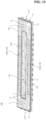
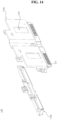
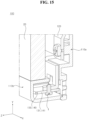
FIGs. 14 and15 in conjunction withFIG. 8 , thefront cover 110b may be coupled to therear cover 110a. Theantenna modules front cover 110b and therear cover 110a. Therear cover 110a may be coupled to the rear surface of theframe 20. Thefront cover 110b may be positioned at the lower side of theframe 20, and may cover the lower side of theframe 20 and/or the lower side of theside frame 30. - The
inner plate 120 may be coupled or fixed to therear cover 110a, and may face the rear surface of theframe 20. Therear cover 110a may have vent holes VH. The vent holes VH may be formed in the rear surface of therear cover 110a. The vent holes VH may be positioned at the rear surface of therear cover 110a so as to correspond to theantenna modules FIG. 8 , therear cover 110a may be fixed to thelower fixing portions frame 10 and/or thebosses antenna modules inner plate 120. Theantenna modules inner plate 120 may be cooled through the vent holes H. - The front surfaces of the
boards antenna modules display device 1. Accordingly, the communication between thedisplay device 1 and thecontrol box 200 may be efficiently performed. - Referring to
FIGs 1 to 15 , the display device may include a display panel, a frame positioned behind the display panel and coupled to the display panel, and a communication box disposed adjacent one side of the frame and coupled to the frame, wherein the communication box may include an inner plate which extends in a vertical direction of the display panel, and an antenna module which defines a flat surface in a direction which intersects the vertical direction of the display panel and is fixed to the inner plate. - The inner plate may include a central plate which faces a rear surface of the frame and a connecting plate which extends toward the antenna module from the central plate, and the connecting plate may include a leg comprising a bent end and is in contact with the flat surface of the antenna module.
- The antenna module may include a PCB and an electrode formed at a flat surface of the PCB, the electrode being disposed so as to face the leg of the connecting plate of the inner plate and being in contact with the leg of the connecting plate of the inner plate.
- The antenna module may further include a shield cover covering a portion of the flat surface of the PCB and fixed to the PCB, and the connecting plate may further include an extension plate which extends toward the antenna module from the central plate and is in contact with the shield cover.
- The communication box may include a rear case coupled to the frame and a front case coupled to the rear case and receiving and covering the antenna module, and the rear case may have at least one vent hole which faces the extension plate.
- The antenna module may include a PCB, a cover frame having an opening which covers a portion of the PCB while exposing another portion of the PCB to an outside, and a first antenna portion positioned on one surface of the PCB and exposed to the outside through the opening in the cover frame, and the first antenna portion may include a plurality of patches sequentially disposed so as to be spaced apart from each other on the one surface of the PCB and a plurality of power feeding portions configured to electrically connect respective ones of the plurality of patches to the PCB.
- The display device may further include a second antenna portion which is positioned at one side of the PCB and which includes a first plurality of dipoles electrically connected to the PCB.
- The display device may further include a third antenna portion which is positioned at another side of the PCB and which includes a second plurality of dipoles electrically connected to the PCB, and a fourth antenna portion which is positioned at a further side of the PCB opposite the third antenna portion based on the PCB and in electrically connected to the PCB and which includes a third plurality of dipoles.
- The number of the first plurality of dipoles may be greater than the number of the second plurality of dipoles or a number of the third plurality of dipoles, and the number of the second plurality of dipoles may correspond to the number of the third plurality of dipoles
- The number of the patches of the first antenna portion may be less than the number of the first plurality of dipoles.
- The first antenna portion may sense a vertical polarization wave, and the second antenna portion may sense a horizontal polarization wave.
- The first antenna portion may sense a horizontal polarization wave, and the second antenna portion may sense a horizontal polarization wave.
- The antenna portion may further include a dummy antenna portion formed at the cover frame, and the dummy antenna portion may eliminate a noise signal.
- The flat surface of the antenna module may define a right degree with respect to the display panel.
- Certain embodiments or other embodiments of the disclosure described above are not mutually exclusive or distinct from each other. Any or all elements of the embodiments of the disclosure described above may be combined with each other in configuration or function.
- For example, a configuration "A" described in one embodiment of the disclosure and the drawings and a configuration "B" described in another embodiment of the disclosure and the drawings may be combined with each other. That is, even if the combination of the configurations is not explicitly described, the combination is possible except in the case where it is stated that the combination is impossible.
- Although embodiments have been described with reference to a number of illustrative embodiments thereof, it should be understood that numerous other modifications and embodiments that fall within the scope of the principles of this disclosure can be devised by those skilled in the art. More particularly, various variations and modifications are possible in the component parts and/or arrangements within the scope of the disclosure, the drawings and the appended claims. In addition to variations and modifications in the component parts and/or arrangements, alternative uses will also be apparent to those skilled in the art.
Claims (14)
- A display device comprising:a display panel;a frame positioned behind the display panel and coupled to the display panel; anda communication box disposed adjacent one side of the frame and coupled to the frame,wherein the communication box comprises:an inner plate which extends in a vertical direction of the display panel; andan antenna module which defines a flat surface in a direction which intersects the vertical direction of the display panel and is fixed to the inner plate.
- The display device according to claim 1, wherein the inner plate comprises:a central plate which faces a rear surface of the frame; anda connecting plate which extends toward the antenna module from the central plate, andwherein the connecting plate comprises a leg comprising a bent end and is in contact with the flat surface of the antenna module.
- The display device according to claim 2, wherein the antenna module comprises:a PCB; andan electrode formed at a flat surface of the PCB, the electrode being disposed so as to face the leg of the connecting plate of the inner plate and being in contact with the leg of the connecting plate of the inner plate.
- The display device according to claim 3, wherein the antenna module further comprises a shield cover covering a portion of the flat surface of the PCB and fixed to the PCB, and
wherein the connecting plate further comprises an extension plate which extends toward the antenna module from the central plate and is in contact with the shield cover. - The display device according to claim 4, wherein the communication box comprises:a rear case coupled to the frame; anda front case coupled to the rear case and receiving and covering the antenna module, andwherein the rear case has at least one vent hole which faces the extension plate.
- The display device according to claim 1, wherein the antenna module comprises:a PCB;a cover frame having an opening which covers a portion of the PCB while exposing another portion of the PCB to an outside; anda first antenna portion positioned on one surface of the PCB and exposed to the outside through the opening in the cover frame, andwherein the first antenna portion comprises:a plurality of patches sequentially disposed so as to be spaced apart from each other on the one surface of the PCB; anda plurality of power feeding portions configured to electrically connect respective ones of the plurality of patches to the PCB.
- The display device according to claim 6, further comprising a second antenna portion which is positioned at one side of the PCB and which includes a first plurality of dipoles electrically connected to the PCB.
- The display device according to claim 7, further comprising:a third antenna portion which is positioned at another side of the PCB and which includes a second plurality of dipoles electrically connected to the PCB; anda fourth antenna portion which is positioned at a further side of the PCB opposite the third antenna portion based on the PCB and in electrically connected to the PCB and which includes a third plurality of dipoles.
- The display device according to claim 8, wherein a number of the first plurality of dipoles is greater than a number of the second plurality of dipoles or a number of the third plurality of dipoles, and
wherein a number of the second plurality of dipoles corresponds to a number of the third plurality of dipoles. - The display device according to claim 9, wherein a number of the patches of the first antenna portion is less than a number of the first plurality of dipoles.
- The display device according to claim 7, wherein the first antenna portion senses a vertical polarization wave, and the second antenna portion senses a horizontal polarization wave.
- The display device according to claim 7, wherein the first antenna portion senses a horizontal polarization wave, and the second antenna portion senses a horizontal polarization wave.
- The display device according to claim 6, wherein the antenna portion further comprises a dummy antenna portion formed at the cover frame, and
wherein the dummy antenna portion eliminates a noise signal. - The display device according to claim 2, wherein the flat surface of the antenna module defines a right degree with respect to the display panel.
Applications Claiming Priority (3)
| Application Number | Priority Date | Filing Date | Title |
|---|---|---|---|
| KR20220074032 | 2022-06-17 | ||
| KR20220074031 | 2022-06-17 | ||
| PCT/KR2023/001310 WO2023243799A1 (en) | 2022-06-17 | 2023-01-27 | Display device |
Publications (2)
| Publication Number | Publication Date |
|---|---|
| EP4478721A1 true EP4478721A1 (en) | 2024-12-18 |
| EP4478721A4 EP4478721A4 (en) | 2025-05-07 |
Family
ID=89191358
Family Applications (1)
| Application Number | Title | Priority Date | Filing Date |
|---|---|---|---|
| EP23824029.5A Pending EP4478721A4 (en) | 2022-06-17 | 2023-01-27 | DISPLAY DEVICE |
Country Status (4)
| Country | Link |
|---|---|
| US (2) | US12355160B2 (en) |
| EP (1) | EP4478721A4 (en) |
| KR (2) | KR102820753B1 (en) |
| WO (1) | WO2023243799A1 (en) |
Families Citing this family (2)
| Publication number | Priority date | Publication date | Assignee | Title |
|---|---|---|---|---|
| KR20260026695A (en) * | 2024-08-20 | 2026-02-27 | 엘지전자 주식회사 | Display device |
| WO2026042983A1 (en) * | 2024-08-20 | 2026-02-26 | 엘지전자 주식회사 | Display device |
Family Cites Families (13)
| Publication number | Priority date | Publication date | Assignee | Title |
|---|---|---|---|---|
| KR20080018059A (en) * | 2006-08-23 | 2008-02-27 | 삼성전자주식회사 | Wireless antenna module and display device and display system equipped with same |
| KR101672738B1 (en) * | 2010-08-31 | 2016-11-07 | 삼성전자 주식회사 | electronic device having cooling structure |
| TWM454040U (en) * | 2012-10-08 | 2013-05-21 | Auden Technology Corp | Display frame antennas |
| JP6008780B2 (en) * | 2013-04-01 | 2016-10-19 | 三菱電機株式会社 | Antenna mounting structure |
| US20150116507A1 (en) * | 2013-10-25 | 2015-04-30 | Ciil Technologies, Llc | Monitoring system for an outdoor display |
| KR102551121B1 (en) * | 2016-09-01 | 2023-07-05 | 엘지전자 주식회사 | Control unit and display device comprising it |
| JP6907039B2 (en) * | 2017-06-14 | 2021-07-21 | キヤノン株式会社 | Display device |
| KR102523265B1 (en) * | 2018-03-28 | 2023-04-21 | 삼성전자주식회사 | Display apparatus |
| TWI704396B (en) * | 2019-08-15 | 2020-09-11 | 啟碁科技股份有限公司 | Electronic display device |
| KR102655173B1 (en) * | 2019-12-20 | 2024-04-08 | 삼성전자주식회사 | Display apparatus |
| KR102665517B1 (en) * | 2019-12-31 | 2024-05-14 | 엘지디스플레이 주식회사 | Cover shield and display device including the same |
| KR102786888B1 (en) * | 2020-06-05 | 2025-03-26 | 삼성전자주식회사 | Electronic device comprising an antenna |
| WO2022045405A1 (en) * | 2020-08-28 | 2022-03-03 | 엘지전자 주식회사 | Display device |
-
2023
- 2023-01-27 WO PCT/KR2023/001310 patent/WO2023243799A1/en not_active Ceased
- 2023-01-27 EP EP23824029.5A patent/EP4478721A4/en active Pending
- 2023-01-27 KR KR1020247017140A patent/KR102820753B1/en active Active
- 2023-01-27 KR KR1020257018643A patent/KR20250086809A/en active Pending
- 2023-01-27 US US18/835,884 patent/US12355160B2/en active Active
-
2025
- 2025-06-11 US US19/234,768 patent/US20250309564A1/en active Pending
Also Published As
| Publication number | Publication date |
|---|---|
| KR102820753B1 (en) | 2025-06-13 |
| US20250149805A1 (en) | 2025-05-08 |
| KR20240095270A (en) | 2024-06-25 |
| US20250309564A1 (en) | 2025-10-02 |
| EP4478721A4 (en) | 2025-05-07 |
| WO2023243799A1 (en) | 2023-12-21 |
| US12355160B2 (en) | 2025-07-08 |
| KR20250086809A (en) | 2025-06-13 |
Similar Documents
| Publication | Publication Date | Title |
|---|---|---|
| US20250309564A1 (en) | Display device | |
| KR101361373B1 (en) | Antennas mounted under dielectric plates | |
| US7535173B2 (en) | Plasma display module | |
| KR101830670B1 (en) | Mobile terminal | |
| CN108648627A (en) | Display panel and its display device | |
| US20250260156A1 (en) | Display device | |
| US12613442B2 (en) | Connector, printed circuit board mounting the connector, and display apparatus including the same | |
| US10485106B2 (en) | Structure for connecting printed circuit board and display apparatus having the same | |
| US20240332782A1 (en) | Display device | |
| US20260121277A1 (en) | Display device | |
| KR20050050836A (en) | Plasma display device | |
| CN118592033A (en) | Display device | |
| EP4700980A1 (en) | Display device | |
| KR102655173B1 (en) | Display apparatus | |
| US20090040450A1 (en) | Circuit board, a liquid crystal display module having the same, and a display device having the same | |
| US20240332783A1 (en) | Display device | |
| KR100844764B1 (en) | Flat panel display | |
| KR102934724B1 (en) | Display device | |
| US20260128498A1 (en) | Display device | |
| US20260075734A1 (en) | Electronic device and display device | |
| CN121999682A (en) | Display device | |
| US20260122798A1 (en) | Display apparatus | |
| KR20260037536A (en) | Electronic device and display device | |
| KR20260061981A (en) | Display device | |
| WO2015087463A1 (en) | Organic el display device |
Legal Events
| Date | Code | Title | Description |
|---|---|---|---|
| STAA | Information on the status of an ep patent application or granted ep patent |
Free format text: STATUS: THE INTERNATIONAL PUBLICATION HAS BEEN MADE |
|
| PUAI | Public reference made under article 153(3) epc to a published international application that has entered the european phase |
Free format text: ORIGINAL CODE: 0009012 |
|
| STAA | Information on the status of an ep patent application or granted ep patent |
Free format text: STATUS: REQUEST FOR EXAMINATION WAS MADE |
|
| 17P | Request for examination filed |
Effective date: 20240913 |
|
| AK | Designated contracting states |
Kind code of ref document: A1 Designated state(s): AL AT BE BG CH CY CZ DE DK EE ES FI FR GB GR HR HU IE IS IT LI LT LU LV MC ME MK MT NL NO PL PT RO RS SE SI SK SM TR |
|
| REG | Reference to a national code |
Ref country code: DE Ref legal event code: R079 Free format text: PREVIOUS MAIN CLASS: H04N0021436300 Ipc: H01Q0001020000 |
|
| A4 | Supplementary search report drawn up and despatched |
Effective date: 20250409 |
|
| RIC1 | Information provided on ipc code assigned before grant |
Ipc: H04N 5/64 20060101ALI20250403BHEP Ipc: H01Q 21/28 20060101ALI20250403BHEP Ipc: H01Q 21/24 20060101ALI20250403BHEP Ipc: H01Q 21/08 20060101ALI20250403BHEP Ipc: H01Q 9/16 20060101ALI20250403BHEP Ipc: H01Q 9/04 20060101ALI20250403BHEP Ipc: H01Q 1/52 20060101ALI20250403BHEP Ipc: H01Q 1/22 20060101ALI20250403BHEP Ipc: H01Q 1/12 20060101ALI20250403BHEP Ipc: H01Q 1/02 20060101AFI20250403BHEP |
|
| DAV | Request for validation of the european patent (deleted) | ||
| DAX | Request for extension of the european patent (deleted) |