EP4478544A1 - Antenna device - Google Patents
Antenna device Download PDFInfo
- Publication number
- EP4478544A1 EP4478544A1 EP24177644.2A EP24177644A EP4478544A1 EP 4478544 A1 EP4478544 A1 EP 4478544A1 EP 24177644 A EP24177644 A EP 24177644A EP 4478544 A1 EP4478544 A1 EP 4478544A1
- Authority
- EP
- European Patent Office
- Prior art keywords
- predetermined
- case
- opening
- antenna element
- main openings
- Prior art date
- Legal status (The legal status is an assumption and is not a legal conclusion. Google has not performed a legal analysis and makes no representation as to the accuracy of the status listed.)
- Granted
Links
Images


Classifications
-
- H—ELECTRICITY
- H01—ELECTRIC ELEMENTS
- H01Q—ANTENNAS, i.e. RADIO AERIALS
- H01Q13/00—Waveguide horns or mouths; Slot antennas; Leaky-waveguide antennas; Equivalent structures causing radiation along the transmission path of a guided wave
- H01Q13/10—Resonant slot antennas
-
- H—ELECTRICITY
- H01—ELECTRIC ELEMENTS
- H01Q—ANTENNAS, i.e. RADIO AERIALS
- H01Q9/00—Electrically-short antennas having dimensions not more than twice the operating wavelength and consisting of conductive active radiating elements
- H01Q9/04—Resonant antennas
- H01Q9/0407—Substantially flat resonant element parallel to ground plane, e.g. patch antenna
-
- H—ELECTRICITY
- H01—ELECTRIC ELEMENTS
- H01Q—ANTENNAS, i.e. RADIO AERIALS
- H01Q5/00—Arrangements for simultaneous operation of antennas on two or more different wavebands, e.g. dual-band or multi-band arrangements
- H01Q5/30—Arrangements for providing operation on different wavebands
- H01Q5/307—Individual or coupled radiating elements, each element being fed in an unspecified way
- H01Q5/314—Individual or coupled radiating elements, each element being fed in an unspecified way using frequency dependent circuits or components, e.g. trap circuits or capacitors
-
- H—ELECTRICITY
- H01—ELECTRIC ELEMENTS
- H01Q—ANTENNAS, i.e. RADIO AERIALS
- H01Q1/00—Details of, or arrangements associated with, antennas
- H01Q1/36—Structural form of radiating elements, e.g. cone, spiral, umbrella; Particular materials used therewith
-
- H—ELECTRICITY
- H01—ELECTRIC ELEMENTS
- H01Q—ANTENNAS, i.e. RADIO AERIALS
- H01Q1/00—Details of, or arrangements associated with, antennas
- H01Q1/42—Housings not intimately mechanically associated with radiating elements, e.g. radome
-
- H—ELECTRICITY
- H01—ELECTRIC ELEMENTS
- H01Q—ANTENNAS, i.e. RADIO AERIALS
- H01Q1/00—Details of, or arrangements associated with, antennas
- H01Q1/50—Structural association of antennas with earthing switches, lead-in devices or lightning protectors
-
- H—ELECTRICITY
- H01—ELECTRIC ELEMENTS
- H01Q—ANTENNAS, i.e. RADIO AERIALS
- H01Q5/00—Arrangements for simultaneous operation of antennas on two or more different wavebands, e.g. dual-band or multi-band arrangements
- H01Q5/10—Resonant antennas
-
- H—ELECTRICITY
- H01—ELECTRIC ELEMENTS
- H01Q—ANTENNAS, i.e. RADIO AERIALS
- H01Q5/00—Arrangements for simultaneous operation of antennas on two or more different wavebands, e.g. dual-band or multi-band arrangements
- H01Q5/20—Arrangements for simultaneous operation of antennas on two or more different wavebands, e.g. dual-band or multi-band arrangements characterised by the operating wavebands
-
- H—ELECTRICITY
- H01—ELECTRIC ELEMENTS
- H01Q—ANTENNAS, i.e. RADIO AERIALS
- H01Q5/00—Arrangements for simultaneous operation of antennas on two or more different wavebands, e.g. dual-band or multi-band arrangements
- H01Q5/30—Arrangements for providing operation on different wavebands
-
- H—ELECTRICITY
- H01—ELECTRIC ELEMENTS
- H01Q—ANTENNAS, i.e. RADIO AERIALS
- H01Q9/00—Electrically-short antennas having dimensions not more than twice the operating wavelength and consisting of conductive active radiating elements
- H01Q9/04—Resonant antennas
- H01Q9/06—Details
Definitions
- Patent Document 1 JP2017-098872A (Patent Document 1), the content of which is incorporated herein by reference.
- the case 92 is an accommodation member for accommodating members such as the antenna element 98 and a circuit board. Considering only necessity of the case 92 as the accommodation member, the case 92 may have a height lower than 60 mm.
- the case 92 should be made higher than the necessary height so that the side plate of the case 92 can be formed with a high opening, or the case 92 should be formed with an opening which extends over an upper and lower plates of this low case 92 as shown in Fig.7 .
- the predetermined opening of an aspect of the present invention works as an LC resonator which has an inductance component mainly formed of the main openings and a capacitance component mainly formed of the coupling opening.
- the thus-formed LC resonator resonates with various radio waves having various frequencies by adjusting the shapes and the sizes of the main openings and the coupling opening, for example, with no change of the height of the case.
- an aspect of the present invention provides the antenna device comprising the case formed with the opening which corresponds to the radio wave of the antenna element and which can be reduced in height.
- the antenna element 42 of the present embodiment is a split-ring resonator formed on the upper surface of the printed circuit board 40. Moreover, the antenna element 42 of the present embodiment is a 2.4 GHz single-band antenna. However, the antenna element 42 of the present invention is not specifically limited. For example, the antenna element 42 may be a dipole antenna. The frequency band of the antenna element 42 is not limited to the 2.4 GHz band.
- the antenna element 42 of the present embodiment is located on the upper surface of the printed circuit board 40 and extends along the horizontal plane.
- the thus-formed antenna element 42 radiates a horizontally polarized wave which has a plane of polarization in parallel to the ground.
- the radio wave radiated from the antenna element 42 has an electric field EF which oscillates in parallel to the ground.
- the present invention is not limited thereto.
- the printed circuit board 40 may extend along a vertical plane (XZ-plane) in parallel to the up-down direction, and the antenna element 42 may extend along the vertical plane.
- the case 20 may be arranged so that the illustrated printed circuit board 40 extends along the vertical plane.
- the antenna element 42 is configured to radiate the radio wave with the predetermined frequency which has a plane of polarization in parallel to a predetermined plane.
- the predetermined plane of the present embodiment is the horizontal plane (XY-plane) in parallel to the ground.
- the present invention is not limited thereto.
- the predetermined plane may be the vertical plane (XZ-plane) perpendicular to the ground.
- the case 20 has a predetermined plate 24.
- the predetermined plate 24 is one of the metal plates 22. More specifically, the predetermined plate 24 is a front plate of the case 20 in a front-rear direction perpendicular to the up-down direction. Thus, the predetermined plate 24 is neither an upper plate nor a lower plate of the case 20.
- the front-rear direction of the present embodiment is the X-direction. In the present embodiment, "forward" means the positive X-direction, and "rearward” means the negative X-direction.
- the predetermined plate 24 is formed with a predetermined opening 30.
- the predetermined opening 30 is a hole which passes through the predetermined plate 24 in the front-rear direction.
- the case 20 is formed with the predetermined opening 30 which is a hole.
- the case 20 of the present embodiment is formed with no hole except for the predetermined opening 30.
- the antenna element 42 of the present embodiment is completely enclosed by the conductive body, or the metal plates 22, except for the predetermined opening 30.
- the present invention is not limited thereto.
- one or more of the metal plates 22 may be formed with a plurality of small holes for discharging heat.
- the predetermined opening 30 has two main openings 32 and a coupling opening 38.
- the two main openings 32 are apart from each other in a first direction perpendicular to the predetermined plane (XY-plane).
- the first direction of the present embodiment is the up-down direction and the Z-direction.
- the first direction is not limited to that of the present embodiment, provided that the first direction is perpendicular to the predetermined plane.
- the predetermined plane may be the XZ-plane
- the first direction may be a lateral direction perpendicular to the predetermined plane (XZ-plane).
- the lateral direction of the present embodiment is the Y-direction.
- the coupling opening 38 couples the two main openings 32 together in the first direction (Z-direction).
- the coupling opening 38 has a size (width WS) smaller than another size of each of the main openings 32 in a second direction (Y-direction) perpendicular to the first direction.
- the predetermined opening 30 with the aforementioned structure works as an LC resonator which has an inductance component L0 mainly formed of the main openings 32 and a capacitance component C0 mainly formed of the coupling opening 38. More specifically, the predetermined opening 30 works as a split-ring resonator.
- the LC resonator which is formed as described above resonates with various radio waves having various frequencies by adjusting the shapes and the sizes of the main openings 32 and the coupling opening 38, for example, with no change of the height of the case 20.
- the resonant frequency of the illustrated LC resonator is inversely proportional to the square root of L0 ⁇ C0.
- L0 becomes larger as the length of inner edge 34 of each of the main openings 32 is made longer and becomes smaller as the length of the inner edge 34 is made shorter.
- the value of C0 becomes smaller as the length LS of the coupling opening 38 is made shorter or as the width WS of the coupling opening 38 is made wider.
- the value of C0 becomes larger as the length LS is made longer or as the width WS is made narrower.
- the resonant frequency of the LC resonator can be made equal to the predetermined frequency of the antenna element 42 by narrowing the width WS while the height of the predetermined opening 30 is kept low.
- the predetermined opening 30 of the present embodiment forms the split-ring resonator which resonates at the predetermined frequency. Moreover, the predetermined opening 30 of the present embodiment is configured to radiate a radio wave, which corresponds to the radio wave radiated from the antenna element 42, outward from the case 20.
- the present embodiment provides the antenna device 10 comprising the case 20 formed with the opening which corresponds to the radio wave of the antenna element 42 and which can be reduced in height.
- the length of the inner edge 34 of each of the illustrated main openings 32 is 59.5 mm.
- the width WS is 0,5 mm, and the length LS is 5 mm.
- the illustrated predetermined opening 30 has a height of 25 mm which is equal to or less than half a necessary height of a slot antenna shown in Fig. 7 .
- the predetermined opening 30 has a reduced height as described above, the predetermined opening 30 can radiate the radio wave with frequency of 2.4 GHz, which corresponds to the antenna element 42 of the present embodiment, outward from the case 20.
- each of the main openings 32 has a rectangular shape.
- the coupling opening 38 linearly extends along the first direction (Z-direction).
- the coupling opening 38 has a first size (length LS) in the first direction and a second size (width WS) in the second direction (Y-direction).
- the first size is larger than the second size.
- the predetermined opening 30 which has a simple shape as described above can be easily formed.
- the present invention is not limited thereto, but the shape of the predetermined opening 30 can be variously modified, provided that the predetermined opening 30 can form a split-ring resonator having a resonant frequency which is equal to the predetermined frequency of the antenna element 42.
- the two main openings 32 of the present embodiment have shapes same as each other.
- the two main openings 32 have congruent shapes same as each other in a plane defined by the first direction (Z-direction) and the second direction (Y-direction).
- the total area of the main openings 32 can be minimized when the resonant frequency of the LC resonator is set to a desired value.
- the predetermined opening 30 can be easily reduced in size in the first direction.
- the present invention is not limited thereto.
- the two main openings 32 may have shapes different from each other.
- the case 20 of the present embodiment is formed of the metal plates 22 as previously described.
- the metal plates 22 of the present embodiment have thicknesses TP same as each other.
- the predetermined plate 24, which is one of the metal plates 22, has the substantially constant thickness TP regardless of its position.
- the size (width WS) of the coupling opening 38 in the second direction (Y-direction) is equal to or less than four times the thickness TP of the metal plate 24. According to this structure, the value of the capacitance component C0 (see Fig. 4 ) formed by the coupling opening 38 can be easily made large.
- the present invention is not limited thereto, but the relationship between the width WS and the thickness TP can be modified as necessary.
- the size (width WS) of the coupling opening 38 in the second direction (Y-direction) is equal to or less than one-fiftieth the length of the inner edge 34 of each of the main openings 32.
- the value of the capacitance component C0 (see Fig. 4 ) formed by the coupling opening 38 can be easily made large.
- the present invention is not limited thereto, but the relationship between the width WS and the length of the inner edge 34 of each of the main openings 32 can be modified as necessary.
- the antenna device 10 can be further variously modified in addition to the already described various modifications.
- the predetermined opening 30 of the present embodiment is visible from outside.
- the predetermined opening 30 may be covered by a cover made of insulator such as resin.
- the predetermined opening 30 may be invisible from outside.
- the antenna element 42 arranged in the case 20 consists of only one single-band antenna, and the number of the predetermined opening 30 formed on the case 20 is one.
- the antenna element 42 may include two or more single-band antennas which radiate radio waves with predetermined frequencies different from each other.
- the antenna element 42 may be a multi-band antenna which radiates two or more radio waves with predetermined frequencies different from each other.
- the case 20 may be formed with two or more of the predetermined openings 30 having resonant frequencies which correspond to two or more predetermined frequencies, respectively.
- the printed circuit board 40 of the present embodiment is located at the middle of the case 20 in the up-down direction.
- the position of the upper surface of the printed circuit board 40 in the up-down direction is equal to the position of the middle point of the coupling opening 38 in the up-down direction.
- the antenna element 42 (see Fig. 5 ) is located at the middle of the coupling opening 38 in the up-down direction.
- This arrangement is preferable from a viewpoint of radiating the radio wave with the predetermined frequency outward from the case 20.
- the present invention is not limited thereto.
- the position of the upper surface of the printed circuit board 40 in the up-down direction may be vertically shifted in some extent relative to the middle point of the coupling opening 38 in the up-down direction.
Landscapes
- Waveguide Aerials (AREA)
- Variable-Direction Aerials And Aerial Arrays (AREA)
Abstract
Description
- This invention relates to an antenna device comprising a case made of conductor and an antenna element arranged in the case.
- For example, this type of antenna device is disclosed in
JP2017-098872A - Referring to
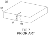
Fig. 7 , Patent Document 1 discloses anantenna device 90 comprising acase 92 formed of metal plates and anantenna element 98 arranged in thecase 92. Thecase 92 has a side plate which is formed with a vertically extendingslot 94. Theslot 94 has a length corresponding to a predetermined frequency which is a frequency of a radio wave radiated from theantenna element 98. Specifically, the length of theslot 94 is designed to be about half a wavelength of the radio wave which has the predetermined frequency. The thus-formedslot 94 resonates with the radio wave radiated from theantenna element 98, and thereby a radio wave with the predetermined frequency is radiated outward from thecase 92. - For example, when the predetermined frequency of the
antenna element 98 is 2.4 GHz, the slot 94 (opening) needs to have a length of about 60 mm. From another viewpoint, thecase 92 is an accommodation member for accommodating members such as theantenna element 98 and a circuit board. Considering only necessity of thecase 92 as the accommodation member, thecase 92 may have a height lower than 60 mm. When the necessary height of the case for accommodating the members is lower than 60 mm, thecase 92 should be made higher than the necessary height so that the side plate of thecase 92 can be formed with a high opening, or thecase 92 should be formed with an opening which extends over an upper and lower plates of thislow case 92 as shown inFig.7 . According to the former solution, the strength of thecase 92 is not greatly lowered, but thecase 92 should be made high at the expense of design flexibility. According to the latter solution, thecase 92 can be reduced in height, but the strength of thecase 92 is lowered because of the opening formed on thecase 92. The height of the opening formed on thecase 92 should be lowered so that both the strength and the design flexibility of thecase 92 are satisfied. - It is therefore an object of the present invention to provide an antenna device comprising a case formed with an opening which corresponds to a radio wave of an antenna element and which can be reduced in height.
- An aspect of the present invention provides an antenna device comprising a case made of conductor and an antenna element. The antenna element is arranged in the case and is configured to radiate a radio wave with a predetermined frequency which has a plane of polarization in parallel to a predetermined plane. The case is formed with a predetermined opening. The predetermined opening has two main openings and a coupling opening. The two main openings are apart from each other in a first direction perpendicular to the predetermined plane. The coupling opening couples the two main openings together in the first direction. The coupling opening has a size smaller than another size of each of the main openings in a second direction perpendicular to the first direction. The predetermined opening forms a split ring resonator which resonates at the predetermined frequency. The predetermined opening is configured to radiate a radio wave, which corresponds to the radio wave radiated from the antenna element, outward from the case.
- The predetermined opening of an aspect of the present invention works as an LC resonator which has an inductance component mainly formed of the main openings and a capacitance component mainly formed of the coupling opening. The thus-formed LC resonator resonates with various radio waves having various frequencies by adjusting the shapes and the sizes of the main openings and the coupling opening, for example, with no change of the height of the case. Thus, an aspect of the present invention provides the antenna device comprising the case formed with the opening which corresponds to the radio wave of the antenna element and which can be reduced in height.
- An appreciation of the objectives of the present invention and a more complete understanding of its structure may be had by studying the following description of the preferred embodiment and by referring to the accompanying drawings.
-
-
Fig. 1 is a perspective view showing an antenna device according to an embodiment of the present invention, wherein a position of an antenna element arranged in a case is illustrated with dashed line. -
Fig. 2 is a front view showing the antenna device ofFig. 1 , wherein a position of an upper surface of a hidden circuit board is illustrated with dashed line. -
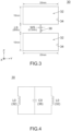
Fig. 3 is a front view showing an example of a predetermined opening of the antenna device ofFig. 2 . -
Fig. 4 is a view showing an LC resonator formed by the predetermined opening ofFig. 3 . -
Fig. 5 is a cross-sectional view showing the antenna device ofFig. 2 , taken along line V-V. -
Fig. 6 is an enlarged, cross-sectional view showing a part of the antenna device enclosed by chain dotted line ofFig. 5 . -
Fig. 7 is a perspective view showing an antenna device of Patent Document 1, wherein an outline of an antenna element arranged in a case is illustrated with dashed line. - While the invention is susceptible to various modifications and alternative forms, specific embodiments thereof are shown by way of example in the drawings and will herein be described in detail. It should be understood, however, that the drawings and detailed description thereto are not intended to limit the invention to the particular form disclosed, but on the contrary, the intention is to cover all modifications, equivalents and alternatives falling within the spirit and scope of the present invention as defined by the appended claims.
- Referring to
Fig. 1 , anantenna device 10 according to an embodiment of the present invention comprises acase 20 made of conductor and anantenna element 42 made of conductor. Thecase 20 of the present embodiment is formed of sixmetal plates 22 connected to each other and has a rectangular parallelepiped shape. Theantenna element 42 of the present embodiment is arranged in thecase 20 and is enclosed by the sixmetal plates 22. Theantenna device 10 of the present embodiment has the aforementioned structure. However, the present invention is not limited thereto. For example, the material and the shape of thecase 20 can be variously modified as necessary. - Referring to
Fig. 5 , theantenna device 10 of the present embodiment comprises a printedcircuit board 40. The printedcircuit board 40 is arranged in thecase 20. Theantenna element 42 is provided on an upper surface of the printedcircuit board 40. The printedcircuit board 40 is provided with afeeding portion 48 in addition to theantenna element 42. Theantenna element 42 radiates a radio wave with a predetermined frequency in response to signals fed by thefeeding portion 48. The printedcircuit board 40 of the present embodiment comprises the aforementioned components. However, the present invention is not limited thereto. For example, theprinted circuit board 40 may comprise various components such as a processing device which sends and receives signals in addition to the aforementioned components. - Referring to
Figs. 5 and 6 , theantenna element 42 of the present embodiment is a split-ring resonator formed on the upper surface of the printedcircuit board 40. Moreover, theantenna element 42 of the present embodiment is a 2.4 GHz single-band antenna. However, theantenna element 42 of the present invention is not specifically limited. For example, theantenna element 42 may be a dipole antenna. The frequency band of theantenna element 42 is not limited to the 2.4 GHz band. - Referring to
Fig. 5 , the printedcircuit board 40 of the present embodiment extends along a horizontal plane perpendicular to an up-down direction. The up-down direction of the present embodiment is the gravity direction and the Z-direction. In the present embodiment, "upward" means the positive Z-direction, and "downward" means the negative Z-direction. The horizontal plane of the present embodiment is the XY-plane. - The
antenna element 42 of the present embodiment is located on the upper surface of the printedcircuit board 40 and extends along the horizontal plane. The thus-formedantenna element 42 radiates a horizontally polarized wave which has a plane of polarization in parallel to the ground. In detail, the radio wave radiated from theantenna element 42 has an electric field EF which oscillates in parallel to the ground. However, the present invention is not limited thereto. For example, the printedcircuit board 40 may extend along a vertical plane (XZ-plane) in parallel to the up-down direction, and theantenna element 42 may extend along the vertical plane. More specifically, thecase 20 may be arranged so that the illustrated printedcircuit board 40 extends along the vertical plane. - Summarizing the explanation described above, the
antenna element 42 is configured to radiate the radio wave with the predetermined frequency which has a plane of polarization in parallel to a predetermined plane. The predetermined plane of the present embodiment is the horizontal plane (XY-plane) in parallel to the ground. However, the present invention is not limited thereto. For example, the predetermined plane may be the vertical plane (XZ-plane) perpendicular to the ground. - As shown in
Figs. 1 and 2 , thecase 20 has a predeterminedplate 24. In the present embodiment, thepredetermined plate 24 is one of themetal plates 22. More specifically, thepredetermined plate 24 is a front plate of thecase 20 in a front-rear direction perpendicular to the up-down direction. Thus, thepredetermined plate 24 is neither an upper plate nor a lower plate of thecase 20. The front-rear direction of the present embodiment is the X-direction. In the present embodiment, "forward" means the positive X-direction, and "rearward" means the negative X-direction. - The
predetermined plate 24 is formed with apredetermined opening 30. Thepredetermined opening 30 is a hole which passes through thepredetermined plate 24 in the front-rear direction. Thus, thecase 20 is formed with thepredetermined opening 30 which is a hole. Thecase 20 of the present embodiment is formed with no hole except for thepredetermined opening 30. Theantenna element 42 of the present embodiment is completely enclosed by the conductive body, or themetal plates 22, except for thepredetermined opening 30. However, the present invention is not limited thereto. For example, one or more of themetal plates 22 may be formed with a plurality of small holes for discharging heat. - Referring to
Figs. 1 to 3 , thepredetermined opening 30 has twomain openings 32 and acoupling opening 38. The twomain openings 32 are apart from each other in a first direction perpendicular to the predetermined plane (XY-plane). The first direction of the present embodiment is the up-down direction and the Z-direction. However, the first direction is not limited to that of the present embodiment, provided that the first direction is perpendicular to the predetermined plane. For example, in an instance where theantenna element 42 radiates a vertically polarized wave, the predetermined plane may be the XZ-plane, and the first direction may be a lateral direction perpendicular to the predetermined plane (XZ-plane). The lateral direction of the present embodiment is the Y-direction. - Referring to
Fig. 3 , the coupling opening 38 couples the twomain openings 32 together in the first direction (Z-direction). Thecoupling opening 38 has a size (width WS) smaller than another size of each of themain openings 32 in a second direction (Y-direction) perpendicular to the first direction. - Referring to
Fig. 4 together withFig. 3 , thepredetermined opening 30 with the aforementioned structure works as an LC resonator which has an inductance component L0 mainly formed of themain openings 32 and a capacitance component C0 mainly formed of thecoupling opening 38. More specifically, thepredetermined opening 30 works as a split-ring resonator. - Referring to
Figs. 5 and 6 together withFigs. 3 and 4 , when the radio wave radiated from theantenna element 42 is propagated to thepredetermined opening 30, an induced current corresponding to the radio wave radiated from theantenna element 42 flows through the inner edge located around thepredetermined opening 30. When the predetermined frequency of the radio wave radiated from theantenna element 42 is substantially equal to the resonant frequency of the LC resonator formed of thepredetermined opening 30, the LC resonator is excited and thereby radiates the radio wave with the predetermined frequency outward from thecase 20. - Referring to
Figs. 1 ,3 and 4 , the LC resonator which is formed as described above resonates with various radio waves having various frequencies by adjusting the shapes and the sizes of themain openings 32 and thecoupling opening 38, for example, with no change of the height of thecase 20. In detail, the resonant frequency of the illustrated LC resonator is inversely proportional to the square root of L0 × C0. The value of L0 becomes larger as the length ofinner edge 34 of each of themain openings 32 is made longer and becomes smaller as the length of theinner edge 34 is made shorter. The value of C0 becomes smaller as the length LS of thecoupling opening 38 is made shorter or as the width WS of thecoupling opening 38 is made wider. The value of C0 becomes larger as the length LS is made longer or as the width WS is made narrower. For example, the resonant frequency of the LC resonator can be made equal to the predetermined frequency of theantenna element 42 by narrowing the width WS while the height of thepredetermined opening 30 is kept low. - As described above, the
predetermined opening 30 of the present embodiment forms the split-ring resonator which resonates at the predetermined frequency. Moreover, thepredetermined opening 30 of the present embodiment is configured to radiate a radio wave, which corresponds to the radio wave radiated from theantenna element 42, outward from thecase 20. The present embodiment provides theantenna device 10 comprising thecase 20 formed with the opening which corresponds to the radio wave of theantenna element 42 and which can be reduced in height. - Referring to
Fig. 3 , the length of theinner edge 34 of each of the illustratedmain openings 32 is 59.5 mm. In the illustratedcoupling opening 38, the width WS is 0,5 mm, and the length LS is 5 mm. The illustratedpredetermined opening 30 has a height of 25 mm which is equal to or less than half a necessary height of a slot antenna shown inFig. 7 . Although thepredetermined opening 30 has a reduced height as described above, thepredetermined opening 30 can radiate the radio wave with frequency of 2.4 GHz, which corresponds to theantenna element 42 of the present embodiment, outward from thecase 20. - According to the present embodiment, each of the
main openings 32 has a rectangular shape. Thecoupling opening 38 linearly extends along the first direction (Z-direction). Thecoupling opening 38 has a first size (length LS) in the first direction and a second size (width WS) in the second direction (Y-direction). The first size is larger than the second size. Thepredetermined opening 30 which has a simple shape as described above can be easily formed. However, the present invention is not limited thereto, but the shape of thepredetermined opening 30 can be variously modified, provided that thepredetermined opening 30 can form a split-ring resonator having a resonant frequency which is equal to the predetermined frequency of theantenna element 42. - The two
main openings 32 of the present embodiment have shapes same as each other. In detail, the twomain openings 32 have congruent shapes same as each other in a plane defined by the first direction (Z-direction) and the second direction (Y-direction). According to this structure, the total area of themain openings 32 can be minimized when the resonant frequency of the LC resonator is set to a desired value. Thus, thepredetermined opening 30 can be easily reduced in size in the first direction. However, the present invention is not limited thereto. For example, the twomain openings 32 may have shapes different from each other. - Referring to
Fig. 6 , thecase 20 of the present embodiment is formed of themetal plates 22 as previously described. Themetal plates 22 of the present embodiment have thicknesses TP same as each other. In particular, thepredetermined plate 24, which is one of themetal plates 22, has the substantially constant thickness TP regardless of its position. The size (width WS) of thecoupling opening 38 in the second direction (Y-direction) is equal to or less than four times the thickness TP of themetal plate 24. According to this structure, the value of the capacitance component C0 (seeFig. 4 ) formed by thecoupling opening 38 can be easily made large. However, the present invention is not limited thereto, but the relationship between the width WS and the thickness TP can be modified as necessary. - Referring to
Fig. 3 , according to the present embodiment, the size (width WS) of thecoupling opening 38 in the second direction (Y-direction) is equal to or less than one-fiftieth the length of theinner edge 34 of each of themain openings 32. According to this structure, the value of the capacitance component C0 (seeFig. 4 ) formed by thecoupling opening 38 can be easily made large. However, the present invention is not limited thereto, but the relationship between the width WS and the length of theinner edge 34 of each of themain openings 32 can be modified as necessary. - Referring to
Fig. 1 , theantenna device 10 can be further variously modified in addition to the already described various modifications. For example, thepredetermined opening 30 of the present embodiment is visible from outside. However, thepredetermined opening 30 may be covered by a cover made of insulator such as resin. In other words, thepredetermined opening 30 may be invisible from outside. - In the present embodiment, the
antenna element 42 arranged in thecase 20 consists of only one single-band antenna, and the number of thepredetermined opening 30 formed on thecase 20 is one. However, the present invention is not limited thereto. For example, theantenna element 42 may include two or more single-band antennas which radiate radio waves with predetermined frequencies different from each other. Theantenna element 42 may be a multi-band antenna which radiates two or more radio waves with predetermined frequencies different from each other. In these instances, thecase 20 may be formed with two or more of thepredetermined openings 30 having resonant frequencies which correspond to two or more predetermined frequencies, respectively. - Referring to
Fig. 2 , the printedcircuit board 40 of the present embodiment is located at the middle of thecase 20 in the up-down direction. In detail, the position of the upper surface of the printedcircuit board 40 in the up-down direction is equal to the position of the middle point of thecoupling opening 38 in the up-down direction. In other words, the antenna element 42 (seeFig. 5 ) is located at the middle of thecoupling opening 38 in the up-down direction. This arrangement is preferable from a viewpoint of radiating the radio wave with the predetermined frequency outward from thecase 20. However, the present invention is not limited thereto. For example, the position of the upper surface of the printedcircuit board 40 in the up-down direction may be vertically shifted in some extent relative to the middle point of thecoupling opening 38 in the up-down direction.
Claims (5)
- An antenna device comprising a case made of conductor and an antenna element, wherein:the antenna element is arranged in the case and is configured to radiate a radio wave with a predetermined frequency which has a plane of polarization in parallel to a predetermined plane;the case is formed with a predetermined opening;the predetermined opening has two main openings and a coupling opening;the two main openings are apart from each other in a first direction perpendicular to the predetermined plane;the coupling opening couples the two main openings together in the first direction;the coupling opening has a size smaller than another size of each of the main openings in a second direction perpendicular to the first direction;the predetermined opening forms a split-ring resonator which resonates at the predetermined frequency; andthe predetermined opening is configured to radiate a radio wave, which corresponds to the radio wave radiated from the antenna element, outward from the case.
- The antenna device as recited in claim 1, wherein:each of the main openings has a rectangular shape;the coupling opening linearly extends along the first direction;the coupling opening has a first size in the first direction and a second size in the second direction; andthe first size is larger than the second size.
- The antenna device as recited in claim 1 or 2, wherein the two main openings have shapes same as each other.
- The antenna device as recited in one of claims 1 to 3, wherein:the case is formed of a metal plate; anda size of the coupling opening in the second direction is equal to or less than four times a thickness of the metal plate.
- The antenna device as recited in one of claims 1 to 4, wherein a size of the coupling opening in the second direction is equal to or less than one-fiftieth a length of an inner edge of each of the main openings.
Applications Claiming Priority (1)
| Application Number | Priority Date | Filing Date | Title |
|---|---|---|---|
| JP2023095980A JP2024177700A (en) | 2023-06-12 | 2023-06-12 | Antenna Device |
Publications (2)
| Publication Number | Publication Date |
|---|---|
| EP4478544A1 true EP4478544A1 (en) | 2024-12-18 |
| EP4478544B1 EP4478544B1 (en) | 2025-12-17 |
Family
ID=91247368
Family Applications (1)
| Application Number | Title | Priority Date | Filing Date |
|---|---|---|---|
| EP24177644.2A Active EP4478544B1 (en) | 2023-06-12 | 2024-05-23 | Antenna device |
Country Status (6)
| Country | Link |
|---|---|
| US (1) | US12665303B2 (en) |
| EP (1) | EP4478544B1 (en) |
| JP (1) | JP2024177700A (en) |
| KR (1) | KR102953196B1 (en) |
| CN (1) | CN119133829A (en) |
| TW (1) | TWI920589B (en) |
Citations (4)
| Publication number | Priority date | Publication date | Assignee | Title |
|---|---|---|---|---|
| US3065752A (en) * | 1959-11-14 | 1962-11-27 | Philips Corp | High frequency therapeutic radiator |
| JP2012175422A (en) * | 2011-02-22 | 2012-09-10 | Nec Corp | Antenna device |
| JP2017098872A (en) | 2015-11-27 | 2017-06-01 | Necプラットフォームズ株式会社 | ANTENNA DEVICE, WIRELESS COMMUNICATION DEVICE, AND ANTENNA FORMING METHOD |
| US20220102874A1 (en) * | 2019-01-30 | 2022-03-31 | Alexander KHRIPKOV | Dual-polarization antenna array |
Family Cites Families (8)
| Publication number | Priority date | Publication date | Assignee | Title |
|---|---|---|---|---|
| JP2012231266A (en) | 2011-04-25 | 2012-11-22 | Fujitsu Component Ltd | Antenna device |
| CN203466286U (en) | 2011-05-23 | 2014-03-05 | 株式会社村田制作所 | Antenna device |
| US9203139B2 (en) | 2012-05-04 | 2015-12-01 | Apple Inc. | Antenna structures having slot-based parasitic elements |
| US9450303B2 (en) * | 2013-11-18 | 2016-09-20 | Inpaq Technology Co., Ltd. | Antenna structure |
| US10186753B2 (en) | 2014-01-31 | 2019-01-22 | Tdk Corporation | Antenna device and portable electronic device using the same |
| CN105006654A (en) | 2015-07-08 | 2015-10-28 | 深圳市信维通信股份有限公司 | Figure-eight-shaped NFC antenna with metal rear housing |
| JP6548271B2 (en) * | 2017-02-06 | 2019-07-24 | Necプラットフォームズ株式会社 | Antenna device and wireless device |
| JP6897989B2 (en) | 2019-01-04 | 2021-07-07 | Necプラットフォームズ株式会社 | Antenna device and wireless device |
-
2023
- 2023-06-12 JP JP2023095980A patent/JP2024177700A/en active Pending
-
2024
- 2024-05-06 CN CN202410546490.9A patent/CN119133829A/en active Pending
- 2024-05-09 KR KR1020240061431A patent/KR102953196B1/en active Active
- 2024-05-21 US US18/669,545 patent/US12665303B2/en active Active
- 2024-05-22 TW TW113118888A patent/TWI920589B/en active
- 2024-05-23 EP EP24177644.2A patent/EP4478544B1/en active Active
Patent Citations (4)
| Publication number | Priority date | Publication date | Assignee | Title |
|---|---|---|---|---|
| US3065752A (en) * | 1959-11-14 | 1962-11-27 | Philips Corp | High frequency therapeutic radiator |
| JP2012175422A (en) * | 2011-02-22 | 2012-09-10 | Nec Corp | Antenna device |
| JP2017098872A (en) | 2015-11-27 | 2017-06-01 | Necプラットフォームズ株式会社 | ANTENNA DEVICE, WIRELESS COMMUNICATION DEVICE, AND ANTENNA FORMING METHOD |
| US20220102874A1 (en) * | 2019-01-30 | 2022-03-31 | Alexander KHRIPKOV | Dual-polarization antenna array |
Also Published As
| Publication number | Publication date |
|---|---|
| TW202504168A (en) | 2025-01-16 |
| CN119133829A (en) | 2024-12-13 |
| KR102953196B1 (en) | 2026-04-15 |
| KR20240175299A (en) | 2024-12-19 |
| US12665303B2 (en) | 2026-06-23 |
| TWI920589B (en) | 2026-04-01 |
| JP2024177700A (en) | 2024-12-24 |
| EP4478544B1 (en) | 2025-12-17 |
| US20240413534A1 (en) | 2024-12-12 |
Similar Documents
| Publication | Publication Date | Title |
|---|---|---|
| EP3471208B1 (en) | Dual band antenna module | |
| US10276934B2 (en) | Antenna structure | |
| KR101709763B1 (en) | Hardened wave-guide antenna | |
| CN112956078A (en) | Three-dimensional inverted-F antenna element, antenna assembly with same and communication system | |
| US6483476B2 (en) | One-piece Yagi-Uda antenna and process for making the same | |
| US20050122267A1 (en) | Internal triple-band antenna | |
| TW201535859A (en) | Multi-band planar inverted-F (PIFA) antennas and systems with improved isolation | |
| US20170250475A1 (en) | Slot antenna with radiator element | |
| US20190229411A1 (en) | Antenna device | |
| CN110574230B (en) | Vehicle-mounted antenna device | |
| US8878742B1 (en) | Dipole with an unbalanced microstrip feed | |
| US6970137B1 (en) | Method and device for loading planar antennas | |
| CN113745811A (en) | Antenna device | |
| US12212050B2 (en) | Antenna device for vehicle | |
| US8519896B2 (en) | Antenna having line-shaped electrode on board end surface | |
| EP3154125B1 (en) | Eight-frequency band antenna | |
| KR20130004430A (en) | Antenna | |
| US10411355B2 (en) | Antenna device | |
| US20240413534A1 (en) | Antenna device | |
| JP2640872B2 (en) | Plate antenna | |
| KR101547027B1 (en) | Internal Antenna for Multi Band | |
| EP2827447A1 (en) | Antenna device | |
| CN117501537B (en) | Dual polarized antenna element for generating millimeter wave frequency radiation | |
| US12142840B2 (en) | Antenna device | |
| TW202420645A (en) | Highly isolated and barely separated antennas integrated with noise free rf-transparent printed circuit board (pcb) for enhanced radiated sensitivity |
Legal Events
| Date | Code | Title | Description |
|---|---|---|---|
| PUAI | Public reference made under article 153(3) epc to a published international application that has entered the european phase |
Free format text: ORIGINAL CODE: 0009012 |
|
| STAA | Information on the status of an ep patent application or granted ep patent |
Free format text: STATUS: THE APPLICATION HAS BEEN PUBLISHED |
|
| AK | Designated contracting states |
Kind code of ref document: A1 Designated state(s): AL AT BE BG CH CY CZ DE DK EE ES FI FR GB GR HR HU IE IS IT LI LT LU LV MC ME MK MT NL NO PL PT RO RS SE SI SK SM TR |
|
| STAA | Information on the status of an ep patent application or granted ep patent |
Free format text: STATUS: REQUEST FOR EXAMINATION WAS MADE |
|
| 17P | Request for examination filed |
Effective date: 20250515 |
|
| GRAP | Despatch of communication of intention to grant a patent |
Free format text: ORIGINAL CODE: EPIDOSNIGR1 |
|
| STAA | Information on the status of an ep patent application or granted ep patent |
Free format text: STATUS: GRANT OF PATENT IS INTENDED |
|
| INTG | Intention to grant announced |
Effective date: 20250721 |
|
| GRAS | Grant fee paid |
Free format text: ORIGINAL CODE: EPIDOSNIGR3 |
|
| GRAA | (expected) grant |
Free format text: ORIGINAL CODE: 0009210 |
|
| STAA | Information on the status of an ep patent application or granted ep patent |
Free format text: STATUS: THE PATENT HAS BEEN GRANTED |
|
| AK | Designated contracting states |
Kind code of ref document: B1 Designated state(s): AL AT BE BG CH CY CZ DE DK EE ES FI FR GB GR HR HU IE IS IT LI LT LU LV MC ME MK MT NL NO PL PT RO RS SE SI SK SM TR |
|
| REG | Reference to a national code |
Ref country code: CH Ref legal event code: F10 Free format text: ST27 STATUS EVENT CODE: U-0-0-F10-F00 (AS PROVIDED BY THE NATIONAL OFFICE) Effective date: 20251217 Ref country code: GB Ref legal event code: FG4D |
|
| REG | Reference to a national code |
Ref country code: DE Ref legal event code: R096 Ref document number: 602024001705 Country of ref document: DE |
|
| REG | Reference to a national code |
Ref country code: LT Ref legal event code: MG9D |
|
| PG25 | Lapsed in a contracting state [announced via postgrant information from national office to epo] |
Ref country code: NO Free format text: LAPSE BECAUSE OF FAILURE TO SUBMIT A TRANSLATION OF THE DESCRIPTION OR TO PAY THE FEE WITHIN THE PRESCRIBED TIME-LIMIT Effective date: 20260317 |
|
| PG25 | Lapsed in a contracting state [announced via postgrant information from national office to epo] |
Ref country code: FI Free format text: LAPSE BECAUSE OF FAILURE TO SUBMIT A TRANSLATION OF THE DESCRIPTION OR TO PAY THE FEE WITHIN THE PRESCRIBED TIME-LIMIT Effective date: 20251217 Ref country code: HR Free format text: LAPSE BECAUSE OF FAILURE TO SUBMIT A TRANSLATION OF THE DESCRIPTION OR TO PAY THE FEE WITHIN THE PRESCRIBED TIME-LIMIT Effective date: 20251217 |
|
| PG25 | Lapsed in a contracting state [announced via postgrant information from national office to epo] |
Ref country code: RS Free format text: LAPSE BECAUSE OF FAILURE TO SUBMIT A TRANSLATION OF THE DESCRIPTION OR TO PAY THE FEE WITHIN THE PRESCRIBED TIME-LIMIT Effective date: 20260317 |
|
| REG | Reference to a national code |
Ref country code: NL Ref legal event code: MP Effective date: 20251217 |
|
| PG25 | Lapsed in a contracting state [announced via postgrant information from national office to epo] |
Ref country code: LV Free format text: LAPSE BECAUSE OF FAILURE TO SUBMIT A TRANSLATION OF THE DESCRIPTION OR TO PAY THE FEE WITHIN THE PRESCRIBED TIME-LIMIT Effective date: 20251217 |
|
| PG25 | Lapsed in a contracting state [announced via postgrant information from national office to epo] |
Ref country code: BG Free format text: LAPSE BECAUSE OF FAILURE TO SUBMIT A TRANSLATION OF THE DESCRIPTION OR TO PAY THE FEE WITHIN THE PRESCRIBED TIME-LIMIT Effective date: 20251217 |
|
| REG | Reference to a national code |
Ref country code: AT Ref legal event code: MK05 Ref document number: 1869428 Country of ref document: AT Kind code of ref document: T Effective date: 20251217 |
|
| PG25 | Lapsed in a contracting state [announced via postgrant information from national office to epo] |
Ref country code: NL Free format text: LAPSE BECAUSE OF FAILURE TO SUBMIT A TRANSLATION OF THE DESCRIPTION OR TO PAY THE FEE WITHIN THE PRESCRIBED TIME-LIMIT Effective date: 20251217 |
|
| PG25 | Lapsed in a contracting state [announced via postgrant information from national office to epo] |
Ref country code: LT Free format text: LAPSE BECAUSE OF FAILURE TO SUBMIT A TRANSLATION OF THE DESCRIPTION OR TO PAY THE FEE WITHIN THE PRESCRIBED TIME-LIMIT Effective date: 20251217 |
|
| PG25 | Lapsed in a contracting state [announced via postgrant information from national office to epo] |
Ref country code: SM Free format text: LAPSE BECAUSE OF FAILURE TO SUBMIT A TRANSLATION OF THE DESCRIPTION OR TO PAY THE FEE WITHIN THE PRESCRIBED TIME-LIMIT Effective date: 20251217 |
|
| PG25 | Lapsed in a contracting state [announced via postgrant information from national office to epo] |
Ref country code: ES Free format text: LAPSE BECAUSE OF FAILURE TO SUBMIT A TRANSLATION OF THE DESCRIPTION OR TO PAY THE FEE WITHIN THE PRESCRIBED TIME-LIMIT Effective date: 20251217 |
|
| PG25 | Lapsed in a contracting state [announced via postgrant information from national office to epo] |
Ref country code: PL Free format text: LAPSE BECAUSE OF FAILURE TO SUBMIT A TRANSLATION OF THE DESCRIPTION OR TO PAY THE FEE WITHIN THE PRESCRIBED TIME-LIMIT Effective date: 20251217 |
|
| PG25 | Lapsed in a contracting state [announced via postgrant information from national office to epo] |
Ref country code: IT Free format text: LAPSE BECAUSE OF FAILURE TO SUBMIT A TRANSLATION OF THE DESCRIPTION OR TO PAY THE FEE WITHIN THE PRESCRIBED TIME-LIMIT Effective date: 20251217 |
|
| PGFP | Annual fee paid to national office [announced via postgrant information from national office to epo] |
Ref country code: DE Payment date: 20260527 Year of fee payment: 3 |
|
| PG25 | Lapsed in a contracting state [announced via postgrant information from national office to epo] |
Ref country code: AT Free format text: LAPSE BECAUSE OF FAILURE TO SUBMIT A TRANSLATION OF THE DESCRIPTION OR TO PAY THE FEE WITHIN THE PRESCRIBED TIME-LIMIT Effective date: 20251217 |
|
| PG25 | Lapsed in a contracting state [announced via postgrant information from national office to epo] |
Ref country code: EE Free format text: LAPSE BECAUSE OF FAILURE TO SUBMIT A TRANSLATION OF THE DESCRIPTION OR TO PAY THE FEE WITHIN THE PRESCRIBED TIME-LIMIT Effective date: 20251217 |
|
| PG25 | Lapsed in a contracting state [announced via postgrant information from national office to epo] |
Ref country code: PT Free format text: LAPSE BECAUSE OF FAILURE TO SUBMIT A TRANSLATION OF THE DESCRIPTION OR TO PAY THE FEE WITHIN THE PRESCRIBED TIME-LIMIT Effective date: 20260417 Ref country code: IS Free format text: LAPSE BECAUSE OF FAILURE TO SUBMIT A TRANSLATION OF THE DESCRIPTION OR TO PAY THE FEE WITHIN THE PRESCRIBED TIME-LIMIT Effective date: 20260417 |
|
| PG25 | Lapsed in a contracting state [announced via postgrant information from national office to epo] |
Ref country code: CZ Free format text: LAPSE BECAUSE OF FAILURE TO SUBMIT A TRANSLATION OF THE DESCRIPTION OR TO PAY THE FEE WITHIN THE PRESCRIBED TIME-LIMIT Effective date: 20251217 |
|
| PGFP | Annual fee paid to national office [announced via postgrant information from national office to epo] |
Ref country code: FR Payment date: 20260508 Year of fee payment: 3 |
|
| PG25 | Lapsed in a contracting state [announced via postgrant information from national office to epo] |
Ref country code: SK Free format text: LAPSE BECAUSE OF FAILURE TO SUBMIT A TRANSLATION OF THE DESCRIPTION OR TO PAY THE FEE WITHIN THE PRESCRIBED TIME-LIMIT Effective date: 20251217 |
|
| PG25 | Lapsed in a contracting state [announced via postgrant information from national office to epo] |
Ref country code: SE Free format text: LAPSE BECAUSE OF FAILURE TO SUBMIT A TRANSLATION OF THE DESCRIPTION OR TO PAY THE FEE WITHIN THE PRESCRIBED TIME-LIMIT Effective date: 20251217 |