EP4478400A1 - Methods for forming a power semiconductor module arrangement - Google Patents
Methods for forming a power semiconductor module arrangement Download PDFInfo
- Publication number
- EP4478400A1 EP4478400A1 EP23178918.1A EP23178918A EP4478400A1 EP 4478400 A1 EP4478400 A1 EP 4478400A1 EP 23178918 A EP23178918 A EP 23178918A EP 4478400 A1 EP4478400 A1 EP 4478400A1
- Authority
- EP
- European Patent Office
- Prior art keywords
- substrate
- potting material
- housing
- irradiating
- forming
- Prior art date
- Legal status (The legal status is an assumption and is not a legal conclusion. Google has not performed a legal analysis and makes no representation as to the accuracy of the status listed.)
- Granted
Links
Images
Classifications
-
- H—ELECTRICITY
- H10—SEMICONDUCTOR DEVICES; ELECTRIC SOLID-STATE DEVICES NOT OTHERWISE PROVIDED FOR
- H10P—GENERIC PROCESSES OR APPARATUS FOR THE MANUFACTURE OR TREATMENT OF DEVICES COVERED BY CLASS H10
- H10P72/00—Handling or holding of wafers, substrates or devices during manufacture or treatment thereof
- H10P72/04—Apparatus for manufacture or treatment
- H10P72/0431—Apparatus for thermal treatment
- H10P72/0436—Apparatus for thermal treatment mainly by radiation
-
- H—ELECTRICITY
- H10—SEMICONDUCTOR DEVICES; ELECTRIC SOLID-STATE DEVICES NOT OTHERWISE PROVIDED FOR
- H10W—GENERIC PACKAGES, INTERCONNECTIONS, CONNECTORS OR OTHER CONSTRUCTIONAL DETAILS OF DEVICES COVERED BY CLASS H10
- H10W76/00—Containers; Fillings or auxiliary members therefor; Seals
- H10W76/01—Manufacture or treatment
- H10W76/05—Providing fillings in containers, e.g. gas filling
-
- H—ELECTRICITY
- H10—SEMICONDUCTOR DEVICES; ELECTRIC SOLID-STATE DEVICES NOT OTHERWISE PROVIDED FOR
- H10W—GENERIC PACKAGES, INTERCONNECTIONS, CONNECTORS OR OTHER CONSTRUCTIONAL DETAILS OF DEVICES COVERED BY CLASS H10
- H10W74/00—Encapsulations, e.g. protective coatings
- H10W74/01—Manufacture or treatment
-
- H—ELECTRICITY
- H10—SEMICONDUCTOR DEVICES; ELECTRIC SOLID-STATE DEVICES NOT OTHERWISE PROVIDED FOR
- H10P—GENERIC PROCESSES OR APPARATUS FOR THE MANUFACTURE OR TREATMENT OF DEVICES COVERED BY CLASS H10
- H10P72/00—Handling or holding of wafers, substrates or devices during manufacture or treatment thereof
- H10P72/04—Apparatus for manufacture or treatment
- H10P72/0438—Apparatus for making assemblies not otherwise provided for, e.g. package constructions
-
- H—ELECTRICITY
- H10—SEMICONDUCTOR DEVICES; ELECTRIC SOLID-STATE DEVICES NOT OTHERWISE PROVIDED FOR
- H10W—GENERIC PACKAGES, INTERCONNECTIONS, CONNECTORS OR OTHER CONSTRUCTIONAL DETAILS OF DEVICES COVERED BY CLASS H10
- H10W40/00—Arrangements for thermal protection or thermal control
- H10W40/20—Arrangements for cooling
- H10W40/25—Arrangements for cooling characterised by their materials
- H10W40/255—Arrangements for cooling characterised by their materials having a laminate or multilayered structure, e.g. direct bond copper [DBC] ceramic substrates
-
- H—ELECTRICITY
- H10—SEMICONDUCTOR DEVICES; ELECTRIC SOLID-STATE DEVICES NOT OTHERWISE PROVIDED FOR
- H10W—GENERIC PACKAGES, INTERCONNECTIONS, CONNECTORS OR OTHER CONSTRUCTIONAL DETAILS OF DEVICES COVERED BY CLASS H10
- H10W74/00—Encapsulations, e.g. protective coatings
- H10W74/10—Encapsulations, e.g. protective coatings characterised by their shape or disposition
- H10W74/111—Encapsulations, e.g. protective coatings characterised by their shape or disposition the semiconductor body being completely enclosed
- H10W74/114—Encapsulations, e.g. protective coatings characterised by their shape or disposition the semiconductor body being completely enclosed by a substrate and the encapsulations
-
- H—ELECTRICITY
- H10—SEMICONDUCTOR DEVICES; ELECTRIC SOLID-STATE DEVICES NOT OTHERWISE PROVIDED FOR
- H10W—GENERIC PACKAGES, INTERCONNECTIONS, CONNECTORS OR OTHER CONSTRUCTIONAL DETAILS OF DEVICES COVERED BY CLASS H10
- H10W76/00—Containers; Fillings or auxiliary members therefor; Seals
- H10W76/10—Containers or parts thereof
-
- H—ELECTRICITY
- H10—SEMICONDUCTOR DEVICES; ELECTRIC SOLID-STATE DEVICES NOT OTHERWISE PROVIDED FOR
- H10W—GENERIC PACKAGES, INTERCONNECTIONS, CONNECTORS OR OTHER CONSTRUCTIONAL DETAILS OF DEVICES COVERED BY CLASS H10
- H10W76/00—Containers; Fillings or auxiliary members therefor; Seals
- H10W76/10—Containers or parts thereof
- H10W76/12—Containers or parts thereof characterised by their shape
- H10W76/15—Containers comprising an insulating or insulated base
-
- H—ELECTRICITY
- H10—SEMICONDUCTOR DEVICES; ELECTRIC SOLID-STATE DEVICES NOT OTHERWISE PROVIDED FOR
- H10W—GENERIC PACKAGES, INTERCONNECTIONS, CONNECTORS OR OTHER CONSTRUCTIONAL DETAILS OF DEVICES COVERED BY CLASS H10
- H10W90/00—Package configurations
-
- H—ELECTRICITY
- H10—SEMICONDUCTOR DEVICES; ELECTRIC SOLID-STATE DEVICES NOT OTHERWISE PROVIDED FOR
- H10W—GENERIC PACKAGES, INTERCONNECTIONS, CONNECTORS OR OTHER CONSTRUCTIONAL DETAILS OF DEVICES COVERED BY CLASS H10
- H10W90/00—Package configurations
- H10W90/701—Package configurations characterised by the relative positions of pads or connectors relative to package parts
Definitions
- the instant disclosure relates to methods for forming a power semiconductor module arrangement, in particular to method for forming a power semiconductor module arrangement comprising an encapsulant.
- Power semiconductor module arrangements often include a substrate within a housing.
- the substrate usually comprises a substrate layer (e.g., a ceramic layer), a first metallization layer deposited on a first side of the substrate layer and, optionally, a second metallization layer deposited on a second side of the substrate layer.
- a semiconductor arrangement including one or more controllable semiconductor elements e.g., two IGBTs in a half-bridge configuration
- One or more terminal elements contact elements
- Power semiconductor modules are known, where the terminal elements are arranged on the substrate and protrude in a direction that is essentially perpendicular to the main surface of the substrate through a cover of the housing.
- the section of the contact elements which protrudes out of the housing may be mechanically and electrically coupled to a printed circuit board.
- the housing may be glued to the substrate in order to remain in a desired position until the substrate is permanently attached to a base plate or heat sink by means of additional connecting elements. Gluing the housing to the substrate, however, requires additional pretreatment steps (e.g., a plasma treatment of the substrate), a step in which the glue is applied to the substrate, as well as a hardening step in which the originally viscous glue is hardened, thereby attaching the housing to the substrate.
- additional pretreatment steps e.g., a plasma treatment of the substrate
- a hardening step in which the originally viscous glue is hardened
- a method for forming a power semiconductor module arrangement includes arranging a housing on a substrate, wherein the housing includes sidewalls and is arranged to directly adjoin the substrate such that the substrate forms a ground surface of the housing, filling a liquid, viscous or semi-liquid UV-curable potting material into the housing, thereby covering the substrate with the potting material, irradiating a first portion of the potting material in areas of the potting material near an interface between the substrate and the sidewalls of the housing so as to seal any gaps between the substrate and the sidewalls of the housing, and irradiating a second portion of the potting material farther away from the interface between the substrate and the sidewalls of the housing than the first portion of the potting material to form an encapsulant, wherein irradiation of the first and second portions of the potting material takes place at different times and/or via different radiation sources .
- Another method for forming a power semiconductor module arrangement includes applying a liquid, viscous or semi-liquid UV-curable potting material to a substrate, irradiating exterior sections along the edges of the substrate with ultraviolet light, thereby triggering a cross-linking of the potting material along the edges of the substrate and forming a dam extending circumferentially along the edges of the substrate, filling a volume defined by the dam with UV-curable potting material, and after forming the dam and filling a volume defined by the dam with UV-curable potting material, irradiating the volume of UV-curable potting material with ultraviolet light, thereby triggering a cross-linking process of the remaining potting material and forming an encapsulant covering the substrate.
- a semiconductor body as described herein may be made from (doped) semiconductor material and may be a semiconductor chip or may be included in a semiconductor chip.
- a semiconductor body has electrically connecting pads and includes at least one semiconductor element with electrodes.
- the power semiconductor module arrangement 100 includes a housing 7 and a substrate 10.
- the substrate 10 includes a dielectric insulation layer 11, a (structured) first metallization layer 111 attached to the dielectric insulation layer 11, and a (structured) second metallization layer 112 attached to the dielectric insulation layer 11.
- the dielectric insulation layer 11 is disposed between the first and second metallization layers 111, 112.
- Each of the first and second metallization layers 111, 112 may consist of or include one of the following materials: copper; a copper alloy; aluminum; an aluminum alloy; any other metal or alloy that remains solid during the operation of the power semiconductor module arrangement.
- the substrate 10 may be a ceramic substrate, that is, a substrate in which the dielectric insulation layer 11 is a ceramic, e.g., a thin ceramic layer.
- the ceramic may consist of or include one of the following materials: aluminum oxide; aluminum nitride; zirconium oxide; silicon nitride; boron nitride; or any other dielectric ceramic.
- the dielectric insulation layer 11 may consist of an organic compound and include one or more of the following materials: Al 2 O 3 , AIN, SiC, BeO, BN, or Si 3 N 4 .
- the substrate 10 may, e.g., be a Direct Copper Bonding (DCB) substrate, a Direct Aluminum Bonding (DAB) substrate, or an Active Metal Brazing (AMB) substrate.
- the substrate 10 may be an Insulated Metal Substrate (IMS).
- An Insulated Metal Substrate generally comprises a dielectric insulation layer 11 comprising (filled) materials such as epoxy resin or polyimide, for example.
- the material of the dielectric insulation layer 11 may be filled with ceramic particles, for example.
- Such particles may comprise, e.g., SiOz, Al 2 O 3 , AlN, SiN or BN and may have a diameter of between about 1 ⁇ m and about 50 ⁇ m.
- the substrate 10 may also be a conventional printed circuit board (PCB) having a non-ceramic dielectric insulation layer 11.
- a non-ceramic dielectric insulation layer 11 may consist of or include a cured resin.
- the substrate 10 is arranged in a housing 7.
- the substrate 10 forms a base surface of the housing 7, while the housing 7 itself solely comprises sidewalls and, optionally, a cover.
- more than one substrate 10 is arranged within the same housing 7.
- One or more semiconductor bodies 20 may be arranged on the at least one substrate 10.
- Each of the semiconductor bodies 20 arranged on the at least one substrate 10 may include a diode, an IGBT (Insulated-Gate Bipolar Transistor), a MOSFET (Metal-Oxide-Semiconductor Field-Effect Transistor), a JFET (Junction Field-Effect Transistor), a HEMT (High-Electron-Mobility Transistor), or any other suitable semiconductor element.
- IGBT Insulated-Gate Bipolar Transistor
- MOSFET Metal-Oxide-Semiconductor Field-Effect Transistor
- JFET Joint Field-Effect Transistor
- HEMT High-Electron-Mobility Transistor
- the one or more semiconductor bodies 20 may form a semiconductor arrangement on the substrate 10.
- the second metallization layer 112 of the substrate 10 in Figure 1 is a continuous layer.
- the second metallization layer 112 may be a structured layer.
- the second metallization layer 112 may be omitted altogether.
- the first metallization layer 111 is a structured layer in the example illustrated in Figure 1 .
- "Structured layer" in this context means that the respective metallization layer is not a continuous layer, but includes recesses between different sections of the layer. Such recesses are schematically illustrated in Figure 1 .
- the first metallization layer 111 in this example includes three different sections.
- Different semiconductor bodies 20 may be mounted to the same or to different sections of the first metallization layer 111. Different sections of the first metallization layer may have no electrical connection or may be electrically connected to one or more other sections using electrical connections 3 such as, e.g., bonding wires. Semiconductor bodies 20 may be electrically connected to each other or to the first metallization layer 111 using electrical connections 3, for example. Electrical connections 3, instead of bonding wires, may also include bonding ribbons, connection plates or conductor rails, for example, to name just a few examples.
- the one or more semiconductor bodies 20 may be electrically and mechanically connected to the substrate 10 by an electrically conductive connection layer 60. Such an electrically conductive connection layer 60 may be a solder layer, a layer of an electrically conductive adhesive, or a layer of a sintered metal powder, e.g., a sintered silver (Ag) powder, for example.
- the power semiconductor module arrangement 100 illustrated in Figure 1 further includes terminal elements 4.
- the terminal elements 4 are mechanically and electrically connected to the substrate 10 (e.g., to the first metallization layer 111) and provide an electrical connection between the inside and the outside of the housing 7.
- the terminal elements 4 may be mechanically and electrically connected to the first metallization layer 111 with a first end 41, while a second end 42 of the terminal elements 4 protrudes out of the housing 7.
- the terminal elements 4 may be electrically contacted from the outside at their second end 42.
- the housing 7 may optionally be provided with a cover comprising a plurality of through holes 72 through which each of the plurality of terminal elements 4 vertically protrudes.
- the components inside the housing 7 may also be electrically contacted from outside the housing 7 in any other suitable way.
- additional terminal elements 4 may be arranged closer to or adjacent to the sidewalls of the housing 7. It is also possible that terminal elements 4 protrude vertically or horizontally through the sidewalls of the housing 7.
- the first end 41 of a terminal element 4 may be electrically and mechanically connected to the substrate 10 by an electrically conductive connection layer, for example (not explicitly illustrated in Figure 1 ).
- an electrically conductive connection layer may be a solder layer, a layer of an electrically conductive adhesive, or a layer of a sintered metal powder, e.g., a sintered silver (Ag) powder, for example.
- the first end 41 of a terminal element 4 may also be electrically coupled to the substrate 10 via one or more electrical connections 3, for example.
- Power semiconductor module arrangements 100 often further include an encapsulant 52.
- the encapsulant 52 may consist of or include a silicone gel or may be a rigid molding compound, for example.
- the encapsulant 52 may at least partly fill the interior of the housing 7, thereby covering the components and electrical connections that are arranged on the substrate 10.
- the terminal elements 4 may be partly embedded in the encapsulant 52. At least their second ends 42, however, are not covered by the encapsulant 52 and protrude from the encapsulant 52 through the housing 7 to the outside of the housing 7.
- the encapsulant 52 is configured to protect the components and electrical connections of the power semiconductor module arrangement 100, in particular the components arranged on the substrate 10 inside the housing 7, from certain environmental conditions and mechanical damage.
- the housing 7 may be glued to the substrate 10 in order to remain in a desired position until the substrate 10 is permanently attached to a base plate or heat sink by means of additional connecting elements.
- the housing 7 may be glued to the substrate 10 before filling a potting material 50 into the housing 7 which, after performing a hardening step, forms the encapsulant 52.
- the power semiconductor module arrangement 100 with the housing 7 glued to the substrate 10 and the encapsulant 52 arranged inside the housing 7 may then be shipped to a customer who then mounts the power semiconductor module arrangement 100 to a support structure such as a base plate or heat sink, for example.
- the power semiconductor module arrangement 100 may be mounted on a support structure (e.g., base plate or heat sink) by means of screws or bolts, for example, which serve to hold the substrate 10 in place and to force its lower surface into contact with the support structure.
- the glued joint between the housing 7 and the substrate 10 is therefore generally not needed to hold the housing 7 in its desired position with regard to the substrate 10 during operation of the power semiconductor module arrangement 100.
- the main purposes of the glued joint are to prevent the potting material 50 forming the encapsulant 52 from leaking out of the housing before being sufficiently hardened and to hold the housing 7 in its desired position with regard to the substrate 10 when shipping the power semiconductor module arrangement 100 to an end customer.
- Gluing the housing 7 to the substrate 10 requires additional pretreatment steps (e.g., a plasma treatment of the substrate 10), a step in which the glue is applied to the substrate 10, as well as a hardening step in which the originally viscous glue is hardened, thereby attaching the housing 7 to the substrate 10.
- additional pretreatment steps e.g., a plasma treatment of the substrate 10
- a hardening step in which the originally viscous glue is hardened
- a method for forming a power semiconductor module arrangement 100 comprises arranging a housing 7 on a substrate 10.
- the housing 7 may be attached to the substrate 10 in any suitable way without a glued joint between the sidewalls of the housing 7 and the substrate 10.
- the housing 7 may be attached to the substrate 10 solely by means of a mechanical connection.
- Such a mechanical connection may be implemented in any suitable way.
- the mechanical connection may be sufficient to attach the housing to the substrate 10 while forming the encapsulant 52 and when shipping the power semiconductor module arrangement 100 to an end customer.
- the power semiconductor module arrangement 100 may comprise specific holding pins that are arranged on the substrate 10 and extend from the substrate 10 in a vertical direction y towards the cover of the housing 7.
- the cover of the housing 7 may comprise holding elements (e.g., sleeves) that are configured to receive a free end of the holding pins, thereby forming a force-fitting connection.
- holding elements e.g., sleeves
- one or more of the terminal elements 4 comprise a holding element arranged between the first end 41 and the second end 42 that is arranged inside a through hole in the cover of the housing 7, wherein each holding element exerts a force on the housing, thereby holding the housing in a desired position with regard to the substrate 10.
- a simple removable clamping mechanism could be used to hold the assembly together.
- Such mechanical connections are only examples.
- a mechanical connection between the housing 7 and the substrate 10 may also be formed in any other suitable way.
- the sidewalls of the housing 7 are arranged on the substrate 10 to directly adjoin the substrate 10 (i.e. a top surface of the substrate 10, wherein the top surface of the substrate 10 may be a top surface of the dielectric insulation layer 11 or a top surface of the first metallization layer 111, wherein the top surface of the dielectric insulation layer 11 is a surface facing the first metallization layer 111, and the top surface of the first metallization layer 111 is a surface the semiconductor bodies 20 and any other elements of the power semiconductor module arrangement 100 are mounted to).
- the potting material 50 that is filled into the housing 7 to form the encapsulant 52 is generally liquid, viscous or semi-liquid before it is hardened to form the encapsulant 52.
- the potting material 50 at least partly fills the housing 7 and covers the substrate 10 and most components mounted thereon, as is schematically illustrated in Figure 2 .
- the terminal elements 4, for example are generally not entirely covered by the potting material 50 and the encapsulant 52, respectively.
- the step of filling the potting material 50 into the housing 7, e.g., by means of a dispensing equipment 80, is schematically illustrated in Figure 2 .
- the dispensing equipment 80 may be arranged centrally above the substrate 10. That is, the potting material 50 is dispensed centrally on the substrate 10 and, from there, spreads towards the edges of the substrate 10.
- the potting material 50 is a UV-curable material.
- UV-curable materials typically include a photoinitiator which, when exposed to UV (ultraviolet) light, initiates cross-linking of the UV-curable material 50, causing it to harden.
- UV curable materials typically cure significantly more quickly than non-UV-curable materials.
- a UV light source 90 may be arranged above the module as shown in Figure 3 , thereby irradiating the UV-curable potting material 50 inside the housing 7 and causing it harden rapidly. This part of the process is typically performed with no lid on top of the housing 7, of course, so that the UV light is able to reach the UV-curable potting material 50.
- the UV-curable potting material 50 has a defined viscosity.
- the viscosity generally depends on the specific potting material 50 that is used to form the encapsulant 52. Such materials may, for example, take the form of epoxy resins or silicone gels.
- a liquid, viscous or semi-liquid UV-curable potting material that is suited to form the encapsulant 52 may have a viscosity of at least 900 mPa*s, for example.
- Some UV-curable potting materials 50 may have a viscosity of 925 mPa*s, others may have a viscosity of 1000 mPa*s, and some may have a viscosity of 8000 mPa*s, for example.
- Viscosity generally is the resistance of a material to a change in shape, or movement of neighboring portions relative to one another. Viscosity denotes opposition to flow. The reciprocal of the viscosity is called the fluidity, a measure of the ease of flow.
- a potting material 50 having a lower viscosity will leak out of the housing 7 faster than a potting material 50 having a higher viscosity.
- At least parts of the power semiconductor module arrangement 100 may be irradiated with ultraviolet light, thereby triggering a cross-linking of the potting material 50.
- a first portion of the potting material 50 may be irradiated in areas of the potting material 50 near an interface between the substrate 10 and the sidewalls of the housing 7 so as to seal any gaps between the substrate 10 and the sidewalls of the housing 7.
- “Near” in this respect refers to any portion of the potting material 50 within a radius of, e.g., up to 5mm (millimeters), up to 10mm, up to 20mm, or even up to 30mm, around the interface between the substrate 10 and the sidewalls of the housing 7.
- At least an edge region (first portion indicated in dashed circles in Figure 3 ) of the substrate 10 may be irradiated with ultraviolet light, such that a cross-linking of the potting material 50 is triggered primarily in areas of the potting material 50 that are closest to the sidewalls of the housing 7.
- the areas closest to where the sidewalls of the housing 7 contact the substrate 10 are the areas where the potting material 50 may potentially leak out of the housing 7.
- the cross-linked potting material 50 itself forms a barrier, seals any gaps between the substrate 10 and the sidewalls of the housing 7, and prevents any potting material 50 that has not yet been cross-linked from leaking out of the housing 7.
- the viscosity of the potting material 50 increases rapidly once the cross-linking has been triggered by means of the ultraviolet light.
- the potting material 50 may change from a liquid, viscous or semi-liquid state to a cured, pasty, hardened or solid state when the cross-linking takes place.
- the method further comprises irradiating a second portion of the potting material 50 farther away from the interface between the substrate 10 and the sidewalls of the housing 7 than the first portion of the potting material 50 to form an encapsulant 52, wherein irradiation of the first and second portions of the potting material takes place at different times and/or via different radiation sources.
- the encapsulant 52 is formed by sufficiently hardening the first and second portion of the potting material 50. This may be achieved solely by irradiating the potting material 50 with ultraviolet light. It is, however, also possible that additional hardening steps follow an initial cross-linking process.
- An additional hardening process may comprise an additional irradiating step, wherein the additional irradiating step comprises irradiating the entire power semiconductor module arrangement 100 with ultraviolet light. It is, however, also possible that the power semiconductor module arrangement 100 is exposed to humidity during an additional hardening process.
- Irradiating the power semiconductor module arrangement 100 may comprise irradiating the power semiconductor module arrangement 100 by means of an ultraviolet light source 90 arranged on a side of the substrate 10 that faces the housing 7 (UV light source 90 arranged above the power semiconductor module arrangement 100 in Figure 3 ).
- an ultraviolet light source 90 arranged on a side of the substrate 10 that faces the housing 7
- the housing 7 can be filled with potting material 50 to a final desired level before irradiating the remaining potting material to rapidly cure it.
- irradiating the power semiconductor module arrangement 100 may comprise irradiating the power semiconductor module arrangement 100 by means of an ultraviolet light source 90 arranged on a side of the substrate 10 that faces away from the housing 7 (UV light source 90 arranged below the power semiconductor module arrangement 100 in Figure 3 ). It is generally possible that the entire power semiconductor module arrangement 100 is equally irradiated by the ultraviolet light. It is, however, generally sufficient to at least irradiate those areas that are closest to the edges of the substrate 10, in order to form a barrier and seal the housing before any potting material 50 can leak out of the housing 7.
- a defined distance or radius d1 from or around the edges of the substrate 10 may be irradiated.
- the defined distance d1 may be, e.g., up to 1cm, up to 2cm or up to 3cm.
- the housing 7 may contact the substrate 10 within this defined distance d1.
- a time that passes between the step of filling the potting material 50 into the housing 7 (filling the potting material 50 into the housing 7 has been completed) and the step of irradiating the first portion of the potting material 50 may depend on the fluidity (or viscosity) of the potting material 50. That is, if the fluidity is high (viscosity is low) the time that passes between filling the potting material 50 into the housing 7 and irradiating the first portion of the potting material 50 may be comparably short, as the potting material 50 may leak out of the housing 7 comparably fast.
- the time that passes between filling the potting material 50 into the housing 7 and irradiating the first portion of the potting material 50 may be comparably long, as the potting material 50 may not leak out of the housing 7 very fast.
- the time that passes between filling the potting material 50 into the housing 7 and irradiating the first portion of the potting material 50 may be zero seconds, up to 30s (seconds), up to one minute or in few cases even up to several minutes, depending on the fluidity of the respective potting material 50.
- the time that passes between filling the potting material 50 into the housing 7 and irradiating the first portion of the potting material 50 may be less than five minutes..
- this irradiation step generally takes significantly less time than the gluing and glue curing steps associated with conventional assembly processes, even when low fluidity gels are used.
- Irradiating the exterior of the semiconductor module housing 7 and of the UV-curable potting material 50 inside the housing 7 may take place simultaneously. Because the volume of the material 50 inside the housing 7 is far greater than the volume of potting material 50 emerging at the interface between the housing 7 and substrate 10, however, curing at the interface (first portion of potting material 50) will complete more rapidly at the external locations.
- the semiconductor module may be irradiated by a UV light source 90 beneath the module and by a further UV light source 90 above the module, for example.
- the UV light source 90 beneath the module may be switched off, while the UV light source 90 above the housing may remain on until the UV-curable potting material 50 inside the housing 7 (second portion of potting material 50) is fully cured.
- the method for forming a power semiconductor module arrangement according to the embodiments described above requires less manufacturing steps than conventional methods. The method, therefore, requires less manufacturing time and is therefore very cost-effective. Any thermal stress which may arise during the step of hardening a glue that attaches the housing 7 to the substrate 10 is entirely avoided by the methods described herein.
- Methods for forming a power semiconductor module arrangement 100 comprising a housing 7 have been described with respect to Figures 1 to 3 above. It is, however, also possible to form a power semiconductor module arrangement 100 without a housing 7 similar to what has been described above.
- the power semiconductor module arrangement 100 as illustrated in Figure 4 comprises a substrate 10 with semiconductor bodies 20 and additional elements (e.g., terminal elements 4, or electrical connections 3) arranged thereon.
- An encapsulant 52 is formed on the substrate 10 by applying a UV-curable potting material 50 to the substrate 10, similar to what has been described above (e.g., by means of a dispensing equipment 80).
- the dispensing equipment 80 may be arranged centrally above the substrate 10. That is, the potting material 50 is dispensed centrally on the substrate 10 and, from there, spreads towards the edges of the substrate 10.
- the exterior sections along the edges of the substrate 10 are irradiated with ultraviolet light (e.g., by means of one or more ultraviolet light sources 90) such that a cross-linking of the UV-curable potting material 50 is triggered as soon as it reaches the edges of the substrate 10.
- a barrier or dam 54 is formed that extends circumferentially along the edges of the substrate 10 which prevents the still liquid, viscous or semi-liquid UV-curable potting material 50 in the central areas of the substrate 10 (inside the volume defined by the dam 54) from flowing off the substrate 10.
- the central areas of the substrate 10, however, are not initially irradiated with ultraviolet light such that the potting material 50 inside the dam 54 can still freely flow inside the volume defined by the dam 54, forming an even layer of potting material 50 within the dam 54.
- the dam 54 may be formed to have a thickness d2 in a horizontal direction of between 0.5cm and 3cm, or between 1cm and 2cm, for example.
- a shading tool or masking tool 84 may be arranged above the substrate 10 (e.g., on a side of the substrate 10 from where the potting material 50 is applied), in order to prevent any ultraviolet light from reaching the central area of the substrate 10.
- One or more ultraviolet light sources 90 may be arranged on the same side of the substrate 10 as the shading or masking tool 84, wherein the shading or masking tool 84 is arranged between the one or more light sources 90 and the substrate 10.
- the dam 54 formed by the cross-linked potting material 50 along the edges of the substrate 10 has been formed and has a desired height h2 (e.g., up to several centimeters) in a vertical direction y, and the volume inside of the dam 54 has been filled with further UV-curable potting material 50, the remaining areas of the substrate 10 may be irradiated with ultraviolet light, thereby triggering a cross-linking of the remaining potting material 50, and forming the encapsulant 52.
- h2 e.g., up to several centimeters
- a housing is arranged on the substrate 10 once the encapsulant 52 has been formed. It is, however, also possible that no housing 7 is mounted to the substrate 10. If, for example, the encapsulant 52 is sufficiently hard (e.g., rigid molding compound), the encapsulant 52 alone may be sufficient in order to protect the substrate 10 and the components mounted thereon from any mechanical damage and any environmental conditions.
- a method for forming a power semiconductor module arrangement 10 comprises applying a liquid, viscous or semi-liquid UV-curable potting material 50 to a substrate 10, irradiating exterior sections along the edges of the substrate 10 with ultraviolet light, thereby triggering a cross-linking of the potting material 50 along the edges of the substrate 10 and forming a dam 54 extending circumferentially along the edges of the substrate 10, filling a volume defined by the dam 54 with UV-curable potting material 50, and, after forming the dam 54 and filling a volume defined by the dam 54 with potting material 50, irradiating the volume of UV-curable potting material 50 with ultraviolet light, thereby triggering a cross-linking process of the remaining potting material 50 and forming an encapsulant 52 covering the substrate 10.
- a cross-linking may be triggered within less than 10 seconds, less than 5 seconds or even within 1 second or less when the potting material 50 is irradiated with ultraviolet light. That is, the cross-linking is started (almost) instantaneously. This is generally not the case when the potting material 50 is hardened by means of a thermal process (e.g., by heating the potting material 50 to a defined temperature). Cross-linking the potting material 50 by means of conventional thermal processes generally requires several minutes or even up to several hours. Once the cross-linking has been triggered, the potting material 50 remains in its current position and any further flow of the potting material 50 is prevented.
- the methods described above by means of Figures 1 to 4 may be performed in a vacuum chamber, for example. In particular, at least one of the irradiating steps may be performed in a vacuum chamber.
Landscapes
- Structures Or Materials For Encapsulating Or Coating Semiconductor Devices Or Solid State Devices (AREA)
Abstract
Description
- The instant disclosure relates to methods for forming a power semiconductor module arrangement, in particular to method for forming a power semiconductor module arrangement comprising an encapsulant.
- Power semiconductor module arrangements often include a substrate within a housing. The substrate usually comprises a substrate layer (e.g., a ceramic layer), a first metallization layer deposited on a first side of the substrate layer and, optionally, a second metallization layer deposited on a second side of the substrate layer. A semiconductor arrangement including one or more controllable semiconductor elements (e.g., two IGBTs in a half-bridge configuration) may be arranged on the substrate. One or more terminal elements (contact elements), which allow for contacting such a semiconductor arrangement from outside the housing, are usually provided. Power semiconductor modules are known, where the terminal elements are arranged on the substrate and protrude in a direction that is essentially perpendicular to the main surface of the substrate through a cover of the housing. The section of the contact elements which protrudes out of the housing may be mechanically and electrically coupled to a printed circuit board. The housing may be glued to the substrate in order to remain in a desired position until the substrate is permanently attached to a base plate or heat sink by means of additional connecting elements. Gluing the housing to the substrate, however, requires additional pretreatment steps (e.g., a plasma treatment of the substrate), a step in which the glue is applied to the substrate, as well as a hardening step in which the originally viscous glue is hardened, thereby attaching the housing to the substrate. Each additional step during the assembly process requires additional process time and increases the overall cost of the power semiconductor module arrangement.
- There is a need for a power semiconductor module arrangement that may be assembled in an effective and cost-efficient way.
- A method for forming a power semiconductor module arrangement includes arranging a housing on a substrate, wherein the housing includes sidewalls and is arranged to directly adjoin the substrate such that the substrate forms a ground surface of the housing, filling a liquid, viscous or semi-liquid UV-curable potting material into the housing, thereby covering the substrate with the potting material, irradiating a first portion of the potting material in areas of the potting material near an interface between the substrate and the sidewalls of the housing so as to seal any gaps between the substrate and the sidewalls of the housing, and irradiating a second portion of the potting material farther away from the interface between the substrate and the sidewalls of the housing than the first portion of the potting material to form an encapsulant, wherein irradiation of the first and second portions of the potting material takes place at different times and/or via different radiation sources .
- Another method for forming a power semiconductor module arrangement includes applying a liquid, viscous or semi-liquid UV-curable potting material to a substrate, irradiating exterior sections along the edges of the substrate with ultraviolet light, thereby triggering a cross-linking of the potting material along the edges of the substrate and forming a dam extending circumferentially along the edges of the substrate, filling a volume defined by the dam with UV-curable potting material, and after forming the dam and filling a volume defined by the dam with UV-curable potting material, irradiating the volume of UV-curable potting material with ultraviolet light, thereby triggering a cross-linking process of the remaining potting material and forming an encapsulant covering the substrate.
- The invention may be better understood with reference to the following drawings and the description. The components in the figures are not necessarily to scale, emphasis instead being placed upon illustrating the principles of the invention. Moreover, in the figures, like referenced numerals designate corresponding parts throughout the different views.
-
-
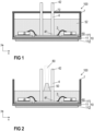
Figure 1 is a cross-sectional view of a power semiconductor module arrangement. -
Figure 2 schematically illustrates a step of a method for forming a power semiconductor module arrangement according to embodiments of the disclosure. -
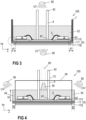
Figure 3 schematically illustrates another step of a method for forming a power semiconductor module arrangement according to embodiments of the disclosure. -
Figure 4 schematically illustrates a step of another method for forming a power semiconductor module arrangement according to embodiments of the disclosure. - In the following detailed description, reference is made to the accompanying drawings. The drawings show specific examples in which the invention may be practiced. It is to be understood that the features and principles described with respect to the various examples may be combined with each other, unless specifically noted otherwise. In the description as well as in the claims, designations of certain elements as "first element", "second element", "third element" etc. are not to be understood as enumerative. Instead, such designations serve solely to address different "elements". That is, e.g., the existence of a "third element" does not require the existence of a "first element" and a "second element". A semiconductor body as described herein may be made from (doped) semiconductor material and may be a semiconductor chip or may be included in a semiconductor chip. A semiconductor body has electrically connecting pads and includes at least one semiconductor element with electrodes.
- Referring to
Figure 1 , a cross-sectional view of a powersemiconductor module arrangement 100 is illustrated. The powersemiconductor module arrangement 100 includes a housing 7 and asubstrate 10. Thesubstrate 10 includes adielectric insulation layer 11, a (structured)first metallization layer 111 attached to thedielectric insulation layer 11, and a (structured)second metallization layer 112 attached to thedielectric insulation layer 11. Thedielectric insulation layer 11 is disposed between the first andsecond metallization layers - Each of the first and
second metallization layers substrate 10 may be a ceramic substrate, that is, a substrate in which thedielectric insulation layer 11 is a ceramic, e.g., a thin ceramic layer. The ceramic may consist of or include one of the following materials: aluminum oxide; aluminum nitride; zirconium oxide; silicon nitride; boron nitride; or any other dielectric ceramic. Alternatively, thedielectric insulation layer 11 may consist of an organic compound and include one or more of the following materials: Al2O3, AIN, SiC, BeO, BN, or Si3N4. For instance, thesubstrate 10 may, e.g., be a Direct Copper Bonding (DCB) substrate, a Direct Aluminum Bonding (DAB) substrate, or an Active Metal Brazing (AMB) substrate. Further, thesubstrate 10 may be an Insulated Metal Substrate (IMS). An Insulated Metal Substrate generally comprises adielectric insulation layer 11 comprising (filled) materials such as epoxy resin or polyimide, for example. The material of thedielectric insulation layer 11 may be filled with ceramic particles, for example. Such particles may comprise, e.g., SiOz, Al2O3, AlN, SiN or BN and may have a diameter of between about 1µm and about 50µm. Thesubstrate 10 may also be a conventional printed circuit board (PCB) having a non-ceramicdielectric insulation layer 11. For instance, a non-ceramicdielectric insulation layer 11 may consist of or include a cured resin. - The
substrate 10 is arranged in a housing 7. In the example illustrated inFigure 1 , thesubstrate 10 forms a base surface of the housing 7, while the housing 7 itself solely comprises sidewalls and, optionally, a cover. In some powersemiconductor module arrangements 100, more than onesubstrate 10 is arranged within the same housing 7. - One or
more semiconductor bodies 20 may be arranged on the at least onesubstrate 10. Each of thesemiconductor bodies 20 arranged on the at least onesubstrate 10 may include a diode, an IGBT (Insulated-Gate Bipolar Transistor), a MOSFET (Metal-Oxide-Semiconductor Field-Effect Transistor), a JFET (Junction Field-Effect Transistor), a HEMT (High-Electron-Mobility Transistor), or any other suitable semiconductor element. - The one or
more semiconductor bodies 20 may form a semiconductor arrangement on thesubstrate 10. InFigure 1 , only twosemiconductor bodies 20 are exemplarily illustrated. Thesecond metallization layer 112 of thesubstrate 10 inFigure 1 is a continuous layer. According to another example, thesecond metallization layer 112 may be a structured layer. According to other examples, thesecond metallization layer 112 may be omitted altogether. Thefirst metallization layer 111 is a structured layer in the example illustrated inFigure 1 . "Structured layer" in this context means that the respective metallization layer is not a continuous layer, but includes recesses between different sections of the layer. Such recesses are schematically illustrated inFigure 1 . Thefirst metallization layer 111 in this example includes three different sections.Different semiconductor bodies 20 may be mounted to the same or to different sections of thefirst metallization layer 111. Different sections of the first metallization layer may have no electrical connection or may be electrically connected to one or more other sections usingelectrical connections 3 such as, e.g., bonding wires.Semiconductor bodies 20 may be electrically connected to each other or to thefirst metallization layer 111 usingelectrical connections 3, for example.Electrical connections 3, instead of bonding wires, may also include bonding ribbons, connection plates or conductor rails, for example, to name just a few examples. The one ormore semiconductor bodies 20 may be electrically and mechanically connected to thesubstrate 10 by an electricallyconductive connection layer 60. Such an electricallyconductive connection layer 60 may be a solder layer, a layer of an electrically conductive adhesive, or a layer of a sintered metal powder, e.g., a sintered silver (Ag) powder, for example. - The power
semiconductor module arrangement 100 illustrated inFigure 1 further includesterminal elements 4. Theterminal elements 4 are mechanically and electrically connected to the substrate 10 (e.g., to the first metallization layer 111) and provide an electrical connection between the inside and the outside of the housing 7. Theterminal elements 4 may be mechanically and electrically connected to thefirst metallization layer 111 with afirst end 41, while asecond end 42 of theterminal elements 4 protrudes out of the housing 7. Theterminal elements 4 may be electrically contacted from the outside at theirsecond end 42. The housing 7 may optionally be provided with a cover comprising a plurality of throughholes 72 through which each of the plurality ofterminal elements 4 vertically protrudes. - In addition to or instead of the
terminal elements 4 described with respect toFigure 1 , the components inside the housing 7 may also be electrically contacted from outside the housing 7 in any other suitable way. For example, additionalterminal elements 4 may be arranged closer to or adjacent to the sidewalls of the housing 7. It is also possible thatterminal elements 4 protrude vertically or horizontally through the sidewalls of the housing 7. Thefirst end 41 of aterminal element 4 may be electrically and mechanically connected to thesubstrate 10 by an electrically conductive connection layer, for example (not explicitly illustrated inFigure 1 ). Such an electrically conductive connection layer may be a solder layer, a layer of an electrically conductive adhesive, or a layer of a sintered metal powder, e.g., a sintered silver (Ag) powder, for example. Thefirst end 41 of aterminal element 4 may also be electrically coupled to thesubstrate 10 via one or moreelectrical connections 3, for example. - Power
semiconductor module arrangements 100 often further include anencapsulant 52. Theencapsulant 52 may consist of or include a silicone gel or may be a rigid molding compound, for example. Theencapsulant 52 may at least partly fill the interior of the housing 7, thereby covering the components and electrical connections that are arranged on thesubstrate 10. Theterminal elements 4 may be partly embedded in theencapsulant 52. At least their second ends 42, however, are not covered by theencapsulant 52 and protrude from theencapsulant 52 through the housing 7 to the outside of the housing 7. Theencapsulant 52 is configured to protect the components and electrical connections of the powersemiconductor module arrangement 100, in particular the components arranged on thesubstrate 10 inside the housing 7, from certain environmental conditions and mechanical damage. - The housing 7 may be glued to the
substrate 10 in order to remain in a desired position until thesubstrate 10 is permanently attached to a base plate or heat sink by means of additional connecting elements. In particular, the housing 7 may be glued to thesubstrate 10 before filling apotting material 50 into the housing 7 which, after performing a hardening step, forms theencapsulant 52. The powersemiconductor module arrangement 100 with the housing 7 glued to thesubstrate 10 and theencapsulant 52 arranged inside the housing 7 may then be shipped to a customer who then mounts the powersemiconductor module arrangement 100 to a support structure such as a base plate or heat sink, for example. The powersemiconductor module arrangement 100 may be mounted on a support structure (e.g., base plate or heat sink) by means of screws or bolts, for example, which serve to hold thesubstrate 10 in place and to force its lower surface into contact with the support structure. The glued joint between the housing 7 and thesubstrate 10 is therefore generally not needed to hold the housing 7 in its desired position with regard to thesubstrate 10 during operation of the powersemiconductor module arrangement 100. The main purposes of the glued joint are to prevent thepotting material 50 forming the encapsulant 52 from leaking out of the housing before being sufficiently hardened and to hold the housing 7 in its desired position with regard to thesubstrate 10 when shipping the powersemiconductor module arrangement 100 to an end customer. Gluing the housing 7 to thesubstrate 10, however, requires additional pretreatment steps (e.g., a plasma treatment of the substrate 10), a step in which the glue is applied to thesubstrate 10, as well as a hardening step in which the originally viscous glue is hardened, thereby attaching the housing 7 to thesubstrate 10. Each additional step during the assembly process requires additional process time and increases the overall cost of the powersemiconductor module arrangement 100. - In the following, methods for forming a power
semiconductor module arrangement 100 according to embodiments of the disclosure will be described in which gluing the housing 7 to thesubstrate 10 is not required. That is, fewer steps are required for the methods described in the following, as compared to conventional methods. In this way, power semiconductor module arrangements can be assembled in a very effective and cost-efficient way. This is, because each additional step of the conventional methods requires time and adds to the overall production costs of a powersemiconductor module arrangement 100. - A method for forming a power
semiconductor module arrangement 100 according to embodiments of the disclosure comprises arranging a housing 7 on asubstrate 10. The housing 7 may be attached to thesubstrate 10 in any suitable way without a glued joint between the sidewalls of the housing 7 and thesubstrate 10. For example, the housing 7 may be attached to thesubstrate 10 solely by means of a mechanical connection. Such a mechanical connection may be implemented in any suitable way. The mechanical connection may be sufficient to attach the housing to thesubstrate 10 while forming theencapsulant 52 and when shipping the powersemiconductor module arrangement 100 to an end customer. For example, the powersemiconductor module arrangement 100 may comprise specific holding pins that are arranged on thesubstrate 10 and extend from thesubstrate 10 in a vertical direction y towards the cover of the housing 7. The cover of the housing 7 may comprise holding elements (e.g., sleeves) that are configured to receive a free end of the holding pins, thereby forming a force-fitting connection. Additionally or alternatively it is also possible, for example, that one or more of theterminal elements 4 comprise a holding element arranged between thefirst end 41 and thesecond end 42 that is arranged inside a through hole in the cover of the housing 7, wherein each holding element exerts a force on the housing, thereby holding the housing in a desired position with regard to thesubstrate 10. Additionally or alternatively, a simple removable clamping mechanism could be used to hold the assembly together. Such mechanical connections, however, are only examples. A mechanical connection between the housing 7 and thesubstrate 10 may also be formed in any other suitable way. - As there is no glue between the housing 7 and the
substrate 10, the sidewalls of the housing 7 (i.e. the lower surfaces of the sidewalls facing the substrate 10) are arranged on thesubstrate 10 to directly adjoin the substrate 10 (i.e. a top surface of thesubstrate 10, wherein the top surface of thesubstrate 10 may be a top surface of thedielectric insulation layer 11 or a top surface of thefirst metallization layer 111, wherein the top surface of thedielectric insulation layer 11 is a surface facing thefirst metallization layer 111, and the top surface of thefirst metallization layer 111 is a surface thesemiconductor bodies 20 and any other elements of the powersemiconductor module arrangement 100 are mounted to). However, when mounting the housing 7 to thesubstrate 10 without a glued joint between the housing 7 and thesubstrate 10, there is a risk that apotting material 50 that is filled into the housing 7 to form the encapsulant leaks out of the housing 7. Small gaps may be present at an interface between the housing 7 and thesubstrate 10. The pottingmaterial 50 that is filled into the housing 7 to form theencapsulant 52 is generally liquid, viscous or semi-liquid before it is hardened to form theencapsulant 52. The pottingmaterial 50 at least partly fills the housing 7 and covers thesubstrate 10 and most components mounted thereon, as is schematically illustrated inFigure 2 . As has been described above, theterminal elements 4, for example, are generally not entirely covered by the pottingmaterial 50 and theencapsulant 52, respectively. The step of filling thepotting material 50 into the housing 7, e.g., by means of adispensing equipment 80, is schematically illustrated inFigure 2 . According to some embodiments of the disclosure, the dispensingequipment 80 may be arranged centrally above thesubstrate 10. That is, the pottingmaterial 50 is dispensed centrally on thesubstrate 10 and, from there, spreads towards the edges of thesubstrate 10. - The potting
material 50 is a UV-curable material. UV-curable materials typically include a photoinitiator which, when exposed to UV (ultraviolet) light, initiates cross-linking of the UV-curable material 50, causing it to harden. UV curable materials typically cure significantly more quickly than non-UV-curable materials. After dispensing thepotting material 50 into the module housing 7 as shown inFigure 2 , aUV light source 90 may be arranged above the module as shown inFigure 3 , thereby irradiating the UV-curable potting material 50 inside the housing 7 and causing it harden rapidly. This part of the process is typically performed with no lid on top of the housing 7, of course, so that the UV light is able to reach the UV-curable potting material 50. - The UV-
curable potting material 50 has a defined viscosity. The viscosity generally depends on thespecific potting material 50 that is used to form theencapsulant 52. Such materials may, for example, take the form of epoxy resins or silicone gels. A liquid, viscous or semi-liquid UV-curable potting material that is suited to form theencapsulant 52 may have a viscosity of at least 900 mPa*s, for example. Some UV-curable potting materials 50 may have a viscosity of 925 mPa*s, others may have a viscosity of 1000 mPa*s, and some may have a viscosity of 8000 mPa*s, for example. Any other viscosity is generally possible. The higher the viscosity of thepotting material 50, the lower its fluidity. Viscosity generally is the resistance of a material to a change in shape, or movement of neighboring portions relative to one another. Viscosity denotes opposition to flow. The reciprocal of the viscosity is called the fluidity, a measure of the ease of flow. A pottingmaterial 50 having a lower viscosity will leak out of the housing 7 faster than a pottingmaterial 50 having a higher viscosity. Generally, there may be significant leakage already within a very short timeframe, e.g., within several tens of seconds, one minute, or two minutes, for example, even when relatively fast-curing UV-curable potting materials are used. - In order to prevent the UV-
curable potting material 50 from leaking out of the housing 7, at least parts of the powersemiconductor module arrangement 100 may be irradiated with ultraviolet light, thereby triggering a cross-linking of thepotting material 50. In particular, a first portion of thepotting material 50 may be irradiated in areas of thepotting material 50 near an interface between thesubstrate 10 and the sidewalls of the housing 7 so as to seal any gaps between thesubstrate 10 and the sidewalls of the housing 7. "Near" in this respect refers to any portion of thepotting material 50 within a radius of, e.g., up to 5mm (millimeters), up to 10mm, up to 20mm, or even up to 30mm, around the interface between thesubstrate 10 and the sidewalls of the housing 7. This is schematically illustrated inFigure 3 . At least an edge region (first portion indicated in dashed circles inFigure 3 ) of thesubstrate 10 may be irradiated with ultraviolet light, such that a cross-linking of thepotting material 50 is triggered primarily in areas of thepotting material 50 that are closest to the sidewalls of the housing 7. The areas closest to where the sidewalls of the housing 7 contact thesubstrate 10 are the areas where thepotting material 50 may potentially leak out of the housing 7. By starting the cross-linking process specifically in these areas, thecross-linked potting material 50 itself forms a barrier, seals any gaps between thesubstrate 10 and the sidewalls of the housing 7, and prevents anypotting material 50 that has not yet been cross-linked from leaking out of the housing 7. The viscosity of thepotting material 50 increases rapidly once the cross-linking has been triggered by means of the ultraviolet light. The pottingmaterial 50 may change from a liquid, viscous or semi-liquid state to a cured, pasty, hardened or solid state when the cross-linking takes place. The method further comprises irradiating a second portion of thepotting material 50 farther away from the interface between thesubstrate 10 and the sidewalls of the housing 7 than the first portion of thepotting material 50 to form anencapsulant 52, wherein irradiation of the first and second portions of the potting material takes place at different times and/or via different radiation sources. - The
encapsulant 52 is formed by sufficiently hardening the first and second portion of thepotting material 50. This may be achieved solely by irradiating thepotting material 50 with ultraviolet light. It is, however, also possible that additional hardening steps follow an initial cross-linking process. An additional hardening process may comprise an additional irradiating step, wherein the additional irradiating step comprises irradiating the entire powersemiconductor module arrangement 100 with ultraviolet light. It is, however, also possible that the powersemiconductor module arrangement 100 is exposed to humidity during an additional hardening process. - Irradiating the power semiconductor module arrangement 100 (e.g., the first portion and/or the second portion of the potting material 50) may comprise irradiating the power
semiconductor module arrangement 100 by means of an ultravioletlight source 90 arranged on a side of thesubstrate 10 that faces the housing 7 (UV light source 90 arranged above the powersemiconductor module arrangement 100 inFigure 3 ). In this case, it may be advantageous to first dispense only a thin layer ofpotting material 50 on thesubstrate 10, sufficient to cover the interface between the housing 7 andsubstrate 10, then to irradiate this thin layer near the edges of thesubstrate 10 to harden thepotting material 50 and seal the interface. Then the housing 7 can be filled withpotting material 50 to a final desired level before irradiating the remaining potting material to rapidly cure it. Alternatively or additionally, irradiating the power semiconductor module arrangement 100 (e.g., the first portion and/or the second portion of the potting material 50) may comprise irradiating the powersemiconductor module arrangement 100 by means of an ultravioletlight source 90 arranged on a side of thesubstrate 10 that faces away from the housing 7 (UV light source 90 arranged below the powersemiconductor module arrangement 100 inFigure 3 ). It is generally possible that the entire powersemiconductor module arrangement 100 is equally irradiated by the ultraviolet light. It is, however, generally sufficient to at least irradiate those areas that are closest to the edges of thesubstrate 10, in order to form a barrier and seal the housing before anypotting material 50 can leak out of the housing 7. For example, at least areas within a defined distance or radius d1 from or around the edges of thesubstrate 10 may be irradiated. The defined distance d1 may be, e.g., up to 1cm, up to 2cm or up to 3cm. The housing 7 may contact thesubstrate 10 within this defined distance d1. Once the cross-linking of thepotting material 50 has been triggered, any gaps between the housing 7 and thesubstrate 10 are sealed solely by means of the resultingencapsulant 52 formed by cross-linking thepotting material 50. - A time that passes between the step of filling the
potting material 50 into the housing 7 (filling thepotting material 50 into the housing 7 has been completed) and the step of irradiating the first portion of thepotting material 50 may depend on the fluidity (or viscosity) of thepotting material 50. That is, if the fluidity is high (viscosity is low) the time that passes between filling thepotting material 50 into the housing 7 and irradiating the first portion of thepotting material 50 may be comparably short, as the pottingmaterial 50 may leak out of the housing 7 comparably fast. If, on the other hand, the fluidity is low (viscosity is high) the time that passes between filling thepotting material 50 into the housing 7 and irradiating the first portion of thepotting material 50 may be comparably long, as the pottingmaterial 50 may not leak out of the housing 7 very fast. Generally, the time that passes between filling thepotting material 50 into the housing 7 and irradiating the first portion of thepotting material 50 may be zero seconds, up to 30s (seconds), up to one minute or in few cases even up to several minutes, depending on the fluidity of therespective potting material 50. For example, the time that passes between filling thepotting material 50 into the housing 7 and irradiating the first portion of thepotting material 50 may be less than five minutes.. However, this irradiation step generally takes significantly less time than the gluing and glue curing steps associated with conventional assembly processes, even when low fluidity gels are used. - Irradiating the exterior of the semiconductor module housing 7 and of the UV-
curable potting material 50 inside the housing 7 may take place simultaneously. Because the volume of thematerial 50 inside the housing 7 is far greater than the volume of pottingmaterial 50 emerging at the interface between the housing 7 andsubstrate 10, however, curing at the interface (first portion of potting material 50) will complete more rapidly at the external locations. The semiconductor module may be irradiated by aUV light source 90 beneath the module and by a furtherUV light source 90 above the module, for example. Once curing is complete at the interface between the housing 7 andsubstrate 10, theUV light source 90 beneath the module may be switched off, while theUV light source 90 above the housing may remain on until the UV-curable potting material 50 inside the housing 7 (second portion of potting material 50) is fully cured. - The method for forming a power semiconductor module arrangement according to the embodiments described above requires less manufacturing steps than conventional methods. The method, therefore, requires less manufacturing time and is therefore very cost-effective. Any thermal stress which may arise during the step of hardening a glue that attaches the housing 7 to the
substrate 10 is entirely avoided by the methods described herein. Methods for forming a powersemiconductor module arrangement 100 comprising a housing 7 have been described with respect toFigures 1 to 3 above. It is, however, also possible to form a powersemiconductor module arrangement 100 without a housing 7 similar to what has been described above. - Now referring to
Figure 4 , methods for forming a powersemiconductor module arrangement 100 without a housing 7 according to embodiments of the disclosure will be described in more detail. The powersemiconductor module arrangement 100 as illustrated inFigure 4 comprises asubstrate 10 withsemiconductor bodies 20 and additional elements (e.g.,terminal elements 4, or electrical connections 3) arranged thereon. Anencapsulant 52 is formed on thesubstrate 10 by applying a UV-curable potting material 50 to thesubstrate 10, similar to what has been described above (e.g., by means of a dispensing equipment 80). According to some embodiments of the disclosure, the dispensingequipment 80 may be arranged centrally above thesubstrate 10. That is, the pottingmaterial 50 is dispensed centrally on thesubstrate 10 and, from there, spreads towards the edges of thesubstrate 10. The exterior sections along the edges of thesubstrate 10 are irradiated with ultraviolet light (e.g., by means of one or more ultraviolet light sources 90) such that a cross-linking of the UV-curable potting material 50 is triggered as soon as it reaches the edges of thesubstrate 10. In this way, a barrier ordam 54 is formed that extends circumferentially along the edges of thesubstrate 10 which prevents the still liquid, viscous or semi-liquid UV-curable potting material 50 in the central areas of the substrate 10 (inside the volume defined by the dam 54) from flowing off thesubstrate 10. The central areas of thesubstrate 10, however, are not initially irradiated with ultraviolet light such that the pottingmaterial 50 inside thedam 54 can still freely flow inside the volume defined by thedam 54, forming an even layer ofpotting material 50 within thedam 54. Thedam 54 may be formed to have a thickness d2 in a horizontal direction of between 0.5cm and 3cm, or between 1cm and 2cm, for example. - A shading tool or masking
tool 84 may be arranged above the substrate 10 (e.g., on a side of thesubstrate 10 from where thepotting material 50 is applied), in order to prevent any ultraviolet light from reaching the central area of thesubstrate 10. One or more ultravioletlight sources 90 may be arranged on the same side of thesubstrate 10 as the shading or maskingtool 84, wherein the shading or maskingtool 84 is arranged between the one or morelight sources 90 and thesubstrate 10. - When the
dam 54 formed by thecross-linked potting material 50 along the edges of thesubstrate 10 has been formed and has a desired height h2 (e.g., up to several centimeters) in a vertical direction y, and the volume inside of thedam 54 has been filled with further UV-curable potting material 50, the remaining areas of thesubstrate 10 may be irradiated with ultraviolet light, thereby triggering a cross-linking of the remainingpotting material 50, and forming theencapsulant 52. - According to some embodiments, a housing is arranged on the
substrate 10 once theencapsulant 52 has been formed. It is, however, also possible that no housing 7 is mounted to thesubstrate 10. If, for example, theencapsulant 52 is sufficiently hard (e.g., rigid molding compound), theencapsulant 52 alone may be sufficient in order to protect thesubstrate 10 and the components mounted thereon from any mechanical damage and any environmental conditions. - Summarizing the above, a method for forming a power
semiconductor module arrangement 10 according to embodiments of the disclosure comprises applying a liquid, viscous or semi-liquid UV-curable potting material 50 to asubstrate 10, irradiating exterior sections along the edges of thesubstrate 10 with ultraviolet light, thereby triggering a cross-linking of thepotting material 50 along the edges of thesubstrate 10 and forming adam 54 extending circumferentially along the edges of thesubstrate 10, filling a volume defined by thedam 54 with UV-curable potting material 50, and, after forming thedam 54 and filling a volume defined by thedam 54 withpotting material 50, irradiating the volume of UV-curable potting material 50 with ultraviolet light, thereby triggering a cross-linking process of the remainingpotting material 50 and forming anencapsulant 52 covering thesubstrate 10. - Depending on the specific materials used as a
potting material 50, a cross-linking may be triggered within less than 10 seconds, less than 5 seconds or even within 1 second or less when the pottingmaterial 50 is irradiated with ultraviolet light. That is, the cross-linking is started (almost) instantaneously. This is generally not the case when the pottingmaterial 50 is hardened by means of a thermal process (e.g., by heating thepotting material 50 to a defined temperature). Cross-linking the pottingmaterial 50 by means of conventional thermal processes generally requires several minutes or even up to several hours. Once the cross-linking has been triggered, the pottingmaterial 50 remains in its current position and any further flow of thepotting material 50 is prevented. The methods described above by means ofFigures 1 to 4 may be performed in a vacuum chamber, for example. In particular, at least one of the irradiating steps may be performed in a vacuum chamber.
Claims (11)
- A method for forming a power semiconductor module arrangement (100), the method comprising:arranging a housing (7) on a substrate (10), wherein the housing (7) comprises sidewalls and is arranged to directly adjoin the substrate (10) such that the substrate (10) forms a ground surface of the housing (7);filling a liquid, viscous or semi-liquid UV-curable potting material (50) into the housing (7), thereby covering the substrate (10) with the potting material (50);irradiating a first portion of the potting material (50) in areas of the potting material (50) near an interface between the substrate (10) and the sidewalls of the housing (7) so as to seal any gaps between the substrate (10) and the sidewalls of the housing (7), andirradiating a second portion of the potting material (50) farther away from the interface between the substrate (10) and the sidewalls of the housing (7) than the first portion of the potting material (50) to form an encapsulant (52), wherein:
irradiation of the first and second portions of the potting material takes place at different times and/or via different radiation sources. - The method of claim 1, wherein irradiating the first portion of the potting material (50) is performed by an ultraviolet light source (90) arranged on a side of the substrate (10) that faces away from the housing (7).
- The method of claim 1 or 2, wherein the second portion of the potting material (50) is performed by an ultraviolet light source (90) arranged on a side of the substrate (10) that faces the housing (7).
- The method of any of claims 1 to 3, wherein the potting material (50) has a defined viscosity, and a time that passes between filling the potting material (50) into the housing (7) and irradiating the first portion of the potting material (50) depends on the viscosity of the potting material (50).
- The method of claim 4, wherein the time that passes between filling the potting material (50) into the housing (7) and irradiating the first portion of the potting material (50) is less than five minutes.
- The method of any of the preceding claims, wherein filling a liquid, viscous or semi-liquid UV-curable potting material (50) into the housing (7) comprises filling a potting material (50) into the housing (7) that has a viscosity of at least 900 mPa*s.
- The method of any of the preceding claims, further comprising, after forming the encapsulant (52) by cross-linking the potting material (50), performing an additional hardening process, thereby further hardening the encapsulant (52).
- The method of any of claims 1 to 7, wherein arranging the housing (7) on the substrate (10) comprises attaching the housing (7) to the substrate (10) by means of a mechanical connection, wherein the housing (7) is attached to the substrate (10) solely by means of the mechanical connection.
- The method of any of the preceding claims, wherein at least one of the irradiation steps is performed in a vacuum chamber.
- A method for forming a power semiconductor module arrangement (100), the method comprising:applying a liquid, viscous or semi-liquid UV-curable potting material (50) to a substrate (10);irradiating exterior sections along the edges of the substrate (10) with ultraviolet light, thereby triggering a cross-linking of the potting material (50) along the edges of the substrate (10) and forming a dam (54) extending circumferentially along the edges of the substrate (10);filling a volume defined by the dam (54) with UV-curable potting material (50); andafter forming the dam (54) and filling a volume defined by the dam (54) with UV-curable potting material (50), irradiating the volume of UV-curable potting material (50) with ultraviolet light, thereby triggering a cross-linking process of the remaining potting material (50) and forming an encapsulant (52) covering the substrate (10).
- The method of claim 10, wherein the dam (54) is formed to have a thickness (d2) in a horizontal direction of between 0.5cm and 3cm, or between 1cm and 2cm.
Priority Applications (3)
| Application Number | Priority Date | Filing Date | Title |
|---|---|---|---|
| EP23178918.1A EP4478400B1 (en) | 2023-06-13 | 2023-06-13 | Method for forming a power semiconductor module arrangement |
| US18/738,124 US20240420968A1 (en) | 2023-06-13 | 2024-06-10 | Methods for forming a power semiconductor module arrangement |
| CN202410750440.2A CN119133002A (en) | 2023-06-13 | 2024-06-12 | Method for forming a power semiconductor module arrangement |
Applications Claiming Priority (1)
| Application Number | Priority Date | Filing Date | Title |
|---|---|---|---|
| EP23178918.1A EP4478400B1 (en) | 2023-06-13 | 2023-06-13 | Method for forming a power semiconductor module arrangement |
Publications (2)
| Publication Number | Publication Date |
|---|---|
| EP4478400A1 true EP4478400A1 (en) | 2024-12-18 |
| EP4478400B1 EP4478400B1 (en) | 2025-07-30 |
Family
ID=86764694
Family Applications (1)
| Application Number | Title | Priority Date | Filing Date |
|---|---|---|---|
| EP23178918.1A Active EP4478400B1 (en) | 2023-06-13 | 2023-06-13 | Method for forming a power semiconductor module arrangement |
Country Status (3)
| Country | Link |
|---|---|
| US (1) | US20240420968A1 (en) |
| EP (1) | EP4478400B1 (en) |
| CN (1) | CN119133002A (en) |
Citations (1)
| Publication number | Priority date | Publication date | Assignee | Title |
|---|---|---|---|---|
| DE102020131493A1 (en) * | 2020-11-27 | 2022-06-02 | Semikron Elektronik Gmbh & Co. Kg | Linked system and method for the internal electrical insulation of a power electronic switching device |
-
2023
- 2023-06-13 EP EP23178918.1A patent/EP4478400B1/en active Active
-
2024
- 2024-06-10 US US18/738,124 patent/US20240420968A1/en active Pending
- 2024-06-12 CN CN202410750440.2A patent/CN119133002A/en active Pending
Patent Citations (1)
| Publication number | Priority date | Publication date | Assignee | Title |
|---|---|---|---|---|
| DE102020131493A1 (en) * | 2020-11-27 | 2022-06-02 | Semikron Elektronik Gmbh & Co. Kg | Linked system and method for the internal electrical insulation of a power electronic switching device |
Also Published As
| Publication number | Publication date |
|---|---|
| CN119133002A (en) | 2024-12-13 |
| EP4478400B1 (en) | 2025-07-30 |
| US20240420968A1 (en) | 2024-12-19 |
Similar Documents
| Publication | Publication Date | Title |
|---|---|---|
| EP3276660A1 (en) | Double-encapsulated power semiconductor module and method for producing the same | |
| US12500152B2 (en) | Power semiconductor module, method for assembling a power semiconductor module and housing for a power semiconductor module | |
| US7723244B2 (en) | Method for internal electrical insulation of a substrate for a power semiconductor module | |
| JP3440824B2 (en) | Semiconductor device | |
| US20030038346A1 (en) | Electronic component having a semiconductor chip, system carrier, and methods for producing the electronic component and the semiconductor chip | |
| CN114078790B (en) | Power semiconductor module device and manufacturing method thereof | |
| EP3477694B1 (en) | Power semiconductor module with partially coated power terminals | |
| EP4478400B1 (en) | Method for forming a power semiconductor module arrangement | |
| EP4270469A1 (en) | Power semiconductor module | |
| US12261063B2 (en) | Method and device for producing a housing | |
| JP2024513524A (en) | Power semiconductor module including molded body and method for manufacturing power semiconductor module | |
| EP4475167A1 (en) | Methods for producing a seal for a semiconductor module, and a housing for a semiconductor module | |
| EP4510181A1 (en) | Power semiconductor module arrangement and method for producing the same | |
| JP7735966B2 (en) | Semiconductor Devices | |
| US20230360982A1 (en) | Method for producing a power semiconductor module | |
| US20260053056A1 (en) | Housing and semiconductor module having a housing | |
| US20230343681A1 (en) | Power Semiconductor Module Arrangements and Methods for Producing Power Semiconductor Module Arrangements | |
| US12107024B2 (en) | Semiconductor device and method of manufacturing semiconductor device | |
| JP2021150575A (en) | Semiconductor device | |
| EP4604176A1 (en) | Semiconductor module arrangement, electronics carrier for a semiconductor module arrangement, and method for producing a semiconductor module arrangement | |
| US20250273520A1 (en) | Housing, semiconductor module having a housing, and method for assembling a semiconductor module | |
| EP4346341A1 (en) | Method for forming a power semiconductor module arrangement | |
| JP2025032597A (en) | Semiconductor module and its manufacturing method | |
| JP2025044484A (en) | Semiconductor device and method for manufacturing semiconductor device | |
| JP2025133524A (en) | Semiconductor Devices |
Legal Events
| Date | Code | Title | Description |
|---|---|---|---|
| PUAI | Public reference made under article 153(3) epc to a published international application that has entered the european phase |
Free format text: ORIGINAL CODE: 0009012 |
|
| STAA | Information on the status of an ep patent application or granted ep patent |
Free format text: STATUS: REQUEST FOR EXAMINATION WAS MADE |
|
| 17P | Request for examination filed |
Effective date: 20240627 |
|
| AK | Designated contracting states |
Kind code of ref document: A1 Designated state(s): AL AT BE BG CH CY CZ DE DK EE ES FI FR GB GR HR HU IE IS IT LI LT LU LV MC ME MK MT NL NO PL PT RO RS SE SI SK SM TR |
|
| GRAP | Despatch of communication of intention to grant a patent |
Free format text: ORIGINAL CODE: EPIDOSNIGR1 |
|
| RIC1 | Information provided on ipc code assigned before grant |
Ipc: H01L 25/07 20060101ALN20250226BHEP Ipc: H01L 23/373 20060101ALN20250226BHEP Ipc: H01L 23/31 20060101ALN20250226BHEP Ipc: H01L 23/053 20060101ALN20250226BHEP Ipc: H01L 21/56 20060101ALI20250226BHEP Ipc: H01L 21/54 20060101AFI20250226BHEP |
|
| STAA | Information on the status of an ep patent application or granted ep patent |
Free format text: STATUS: GRANT OF PATENT IS INTENDED |
|
| RIC1 | Information provided on ipc code assigned before grant |
Ipc: H01L 23/498 20060101ALN20250320BHEP Ipc: H01L 25/07 20060101ALN20250320BHEP Ipc: H01L 23/373 20060101ALN20250320BHEP Ipc: H01L 23/31 20060101ALN20250320BHEP Ipc: H01L 23/053 20060101ALN20250320BHEP Ipc: H01L 21/56 20060101ALI20250320BHEP Ipc: H01L 21/54 20060101AFI20250320BHEP |
|
| INTG | Intention to grant announced |
Effective date: 20250403 |
|
| GRAS | Grant fee paid |
Free format text: ORIGINAL CODE: EPIDOSNIGR3 |
|
| GRAA | (expected) grant |
Free format text: ORIGINAL CODE: 0009210 |
|
| STAA | Information on the status of an ep patent application or granted ep patent |
Free format text: STATUS: THE PATENT HAS BEEN GRANTED |
|
| P01 | Opt-out of the competence of the unified patent court (upc) registered |
Free format text: CASE NUMBER: APP_24580/2025 Effective date: 20250522 |
|
| AK | Designated contracting states |
Kind code of ref document: B1 Designated state(s): AL AT BE BG CH CY CZ DE DK EE ES FI FR GB GR HR HU IE IS IT LI LT LU LV MC ME MK MT NL NO PL PT RO RS SE SI SK SM TR |
|
| REG | Reference to a national code |
Ref country code: GB Ref legal event code: FG4D |
|
| REG | Reference to a national code |
Ref country code: CH Ref legal event code: EP |
|
| REG | Reference to a national code |
Ref country code: DE Ref legal event code: R096 Ref document number: 602023005167 Country of ref document: DE |
|
| REG | Reference to a national code |
Ref country code: IE Ref legal event code: FG4D |
|
| REG | Reference to a national code |
Ref country code: DE Ref legal event code: R079 Ref document number: 602023005167 Country of ref document: DE Free format text: PREVIOUS MAIN CLASS: H01L0021540000 Ipc: H10W0076050000 |
|
| REG | Reference to a national code |
Ref country code: NL Ref legal event code: MP Effective date: 20250730 |
|
| REG | Reference to a national code |
Ref country code: AT Ref legal event code: MK05 Ref document number: 1819998 Country of ref document: AT Kind code of ref document: T Effective date: 20250730 |
|
| PG25 | Lapsed in a contracting state [announced via postgrant information from national office to epo] |
Ref country code: PT Free format text: LAPSE BECAUSE OF FAILURE TO SUBMIT A TRANSLATION OF THE DESCRIPTION OR TO PAY THE FEE WITHIN THE PRESCRIBED TIME-LIMIT Effective date: 20251202 |
|
| PG25 | Lapsed in a contracting state [announced via postgrant information from national office to epo] |
Ref country code: IS Free format text: LAPSE BECAUSE OF FAILURE TO SUBMIT A TRANSLATION OF THE DESCRIPTION OR TO PAY THE FEE WITHIN THE PRESCRIBED TIME-LIMIT Effective date: 20251130 |
|
| PG25 | Lapsed in a contracting state [announced via postgrant information from national office to epo] |
Ref country code: NO Free format text: LAPSE BECAUSE OF FAILURE TO SUBMIT A TRANSLATION OF THE DESCRIPTION OR TO PAY THE FEE WITHIN THE PRESCRIBED TIME-LIMIT Effective date: 20251030 |
|
| REG | Reference to a national code |
Ref country code: LT Ref legal event code: MG9D |
|
| PG25 | Lapsed in a contracting state [announced via postgrant information from national office to epo] |
Ref country code: AT Free format text: LAPSE BECAUSE OF FAILURE TO SUBMIT A TRANSLATION OF THE DESCRIPTION OR TO PAY THE FEE WITHIN THE PRESCRIBED TIME-LIMIT Effective date: 20250730 |
|
| PG25 | Lapsed in a contracting state [announced via postgrant information from national office to epo] |
Ref country code: FI Free format text: LAPSE BECAUSE OF FAILURE TO SUBMIT A TRANSLATION OF THE DESCRIPTION OR TO PAY THE FEE WITHIN THE PRESCRIBED TIME-LIMIT Effective date: 20250730 |
|
| PG25 | Lapsed in a contracting state [announced via postgrant information from national office to epo] |
Ref country code: NL Free format text: LAPSE BECAUSE OF FAILURE TO SUBMIT A TRANSLATION OF THE DESCRIPTION OR TO PAY THE FEE WITHIN THE PRESCRIBED TIME-LIMIT Effective date: 20250730 Ref country code: HR Free format text: LAPSE BECAUSE OF FAILURE TO SUBMIT A TRANSLATION OF THE DESCRIPTION OR TO PAY THE FEE WITHIN THE PRESCRIBED TIME-LIMIT Effective date: 20250730 |
|
| PG25 | Lapsed in a contracting state [announced via postgrant information from national office to epo] |
Ref country code: GR Free format text: LAPSE BECAUSE OF FAILURE TO SUBMIT A TRANSLATION OF THE DESCRIPTION OR TO PAY THE FEE WITHIN THE PRESCRIBED TIME-LIMIT Effective date: 20251031 |
|
| PG25 | Lapsed in a contracting state [announced via postgrant information from national office to epo] |
Ref country code: SE Free format text: LAPSE BECAUSE OF FAILURE TO SUBMIT A TRANSLATION OF THE DESCRIPTION OR TO PAY THE FEE WITHIN THE PRESCRIBED TIME-LIMIT Effective date: 20250730 |
|
| PG25 | Lapsed in a contracting state [announced via postgrant information from national office to epo] |
Ref country code: LV Free format text: LAPSE BECAUSE OF FAILURE TO SUBMIT A TRANSLATION OF THE DESCRIPTION OR TO PAY THE FEE WITHIN THE PRESCRIBED TIME-LIMIT Effective date: 20250730 |
|
| PG25 | Lapsed in a contracting state [announced via postgrant information from national office to epo] |
Ref country code: PL Free format text: LAPSE BECAUSE OF FAILURE TO SUBMIT A TRANSLATION OF THE DESCRIPTION OR TO PAY THE FEE WITHIN THE PRESCRIBED TIME-LIMIT Effective date: 20250730 Ref country code: BG Free format text: LAPSE BECAUSE OF FAILURE TO SUBMIT A TRANSLATION OF THE DESCRIPTION OR TO PAY THE FEE WITHIN THE PRESCRIBED TIME-LIMIT Effective date: 20250730 |
|
| PG25 | Lapsed in a contracting state [announced via postgrant information from national office to epo] |
Ref country code: RS Free format text: LAPSE BECAUSE OF FAILURE TO SUBMIT A TRANSLATION OF THE DESCRIPTION OR TO PAY THE FEE WITHIN THE PRESCRIBED TIME-LIMIT Effective date: 20251030 |
|
| PG25 | Lapsed in a contracting state [announced via postgrant information from national office to epo] |
Ref country code: ES Free format text: LAPSE BECAUSE OF FAILURE TO SUBMIT A TRANSLATION OF THE DESCRIPTION OR TO PAY THE FEE WITHIN THE PRESCRIBED TIME-LIMIT Effective date: 20250730 |
|
| PG25 | Lapsed in a contracting state [announced via postgrant information from national office to epo] |
Ref country code: SM Free format text: LAPSE BECAUSE OF FAILURE TO SUBMIT A TRANSLATION OF THE DESCRIPTION OR TO PAY THE FEE WITHIN THE PRESCRIBED TIME-LIMIT Effective date: 20250730 |
|
| PG25 | Lapsed in a contracting state [announced via postgrant information from national office to epo] |
Ref country code: DK Free format text: LAPSE BECAUSE OF FAILURE TO SUBMIT A TRANSLATION OF THE DESCRIPTION OR TO PAY THE FEE WITHIN THE PRESCRIBED TIME-LIMIT Effective date: 20250730 |
|
| PG25 | Lapsed in a contracting state [announced via postgrant information from national office to epo] |
Ref country code: IT Free format text: LAPSE BECAUSE OF FAILURE TO SUBMIT A TRANSLATION OF THE DESCRIPTION OR TO PAY THE FEE WITHIN THE PRESCRIBED TIME-LIMIT Effective date: 20250730 |
|
| PG25 | Lapsed in a contracting state [announced via postgrant information from national office to epo] |
Ref country code: CZ Free format text: LAPSE BECAUSE OF FAILURE TO SUBMIT A TRANSLATION OF THE DESCRIPTION OR TO PAY THE FEE WITHIN THE PRESCRIBED TIME-LIMIT Effective date: 20250730 |
|
| PG25 | Lapsed in a contracting state [announced via postgrant information from national office to epo] |
Ref country code: EE Free format text: LAPSE BECAUSE OF FAILURE TO SUBMIT A TRANSLATION OF THE DESCRIPTION OR TO PAY THE FEE WITHIN THE PRESCRIBED TIME-LIMIT Effective date: 20250730 Ref country code: SK Free format text: LAPSE BECAUSE OF FAILURE TO SUBMIT A TRANSLATION OF THE DESCRIPTION OR TO PAY THE FEE WITHIN THE PRESCRIBED TIME-LIMIT Effective date: 20250730 |