EP4478117A1 - Display device - Google Patents
Display device Download PDFInfo
- Publication number
- EP4478117A1 EP4478117A1 EP24174315.2A EP24174315A EP4478117A1 EP 4478117 A1 EP4478117 A1 EP 4478117A1 EP 24174315 A EP24174315 A EP 24174315A EP 4478117 A1 EP4478117 A1 EP 4478117A1
- Authority
- EP
- European Patent Office
- Prior art keywords
- line
- opening
- rear plate
- line filter
- display device
- Prior art date
- Legal status (The legal status is an assumption and is not a legal conclusion. Google has not performed a legal analysis and makes no representation as to the accuracy of the status listed.)
- Pending
Links
Images







Classifications
-
- G—PHYSICS
- G09—EDUCATION; CRYPTOGRAPHY; DISPLAY; ADVERTISING; SEALS
- G09F—DISPLAYING; ADVERTISING; SIGNS; LABELS OR NAME-PLATES; SEALS
- G09F9/00—Indicating arrangements for variable information in which the information is built-up on a support by selection or combination of individual elements
- G09F9/30—Indicating arrangements for variable information in which the information is built-up on a support by selection or combination of individual elements in which the desired character or characters are formed by combining individual elements
-
- H—ELECTRICITY
- H10—SEMICONDUCTOR DEVICES; ELECTRIC SOLID-STATE DEVICES NOT OTHERWISE PROVIDED FOR
- H10K—ORGANIC ELECTRIC SOLID-STATE DEVICES
- H10K59/00—Integrated devices, or assemblies of multiple devices, comprising at least one organic light-emitting element covered by group H10K50/00
- H10K59/80—Constructional details
- H10K59/87—Passivation; Containers; Encapsulations
- H10K59/871—Self-supporting sealing arrangements
- H10K59/872—Containers
-
- G—PHYSICS
- G09—EDUCATION; CRYPTOGRAPHY; DISPLAY; ADVERTISING; SEALS
- G09F—DISPLAYING; ADVERTISING; SIGNS; LABELS OR NAME-PLATES; SEALS
- G09F9/00—Indicating arrangements for variable information in which the information is built-up on a support by selection or combination of individual elements
- G09F9/30—Indicating arrangements for variable information in which the information is built-up on a support by selection or combination of individual elements in which the desired character or characters are formed by combining individual elements
- G09F9/33—Indicating arrangements for variable information in which the information is built-up on a support by selection or combination of individual elements in which the desired character or characters are formed by combining individual elements being semiconductor devices, e.g. diodes
- G09F9/335—Indicating arrangements for variable information in which the information is built-up on a support by selection or combination of individual elements in which the desired character or characters are formed by combining individual elements being semiconductor devices, e.g. diodes being organic light emitting diodes [OLED]
-
- G—PHYSICS
- G02—OPTICS
- G02F—OPTICAL DEVICES OR ARRANGEMENTS FOR THE CONTROL OF LIGHT BY MODIFICATION OF THE OPTICAL PROPERTIES OF THE MEDIA OF THE ELEMENTS INVOLVED THEREIN; NON-LINEAR OPTICS; FREQUENCY-CHANGING OF LIGHT; OPTICAL LOGIC ELEMENTS; OPTICAL ANALOGUE/DIGITAL CONVERTERS
- G02F1/00—Devices or arrangements for the control of the intensity, colour, phase, polarisation or direction of light arriving from an independent light source, e.g. switching, gating or modulating; Non-linear optics
- G02F1/01—Devices or arrangements for the control of the intensity, colour, phase, polarisation or direction of light arriving from an independent light source, e.g. switching, gating or modulating; Non-linear optics for the control of the intensity, phase, polarisation or colour
- G02F1/13—Devices or arrangements for the control of the intensity, colour, phase, polarisation or direction of light arriving from an independent light source, e.g. switching, gating or modulating; Non-linear optics for the control of the intensity, phase, polarisation or colour based on liquid crystals, e.g. single liquid crystal display cells
- G02F1/133—Constructional arrangements; Operation of liquid crystal cells; Circuit arrangements
- G02F1/1333—Constructional arrangements; Manufacturing methods
- G02F1/133308—Support structures for LCD panels, e.g. frames or bezels
-
- G—PHYSICS
- G02—OPTICS
- G02F—OPTICAL DEVICES OR ARRANGEMENTS FOR THE CONTROL OF LIGHT BY MODIFICATION OF THE OPTICAL PROPERTIES OF THE MEDIA OF THE ELEMENTS INVOLVED THEREIN; NON-LINEAR OPTICS; FREQUENCY-CHANGING OF LIGHT; OPTICAL LOGIC ELEMENTS; OPTICAL ANALOGUE/DIGITAL CONVERTERS
- G02F1/00—Devices or arrangements for the control of the intensity, colour, phase, polarisation or direction of light arriving from an independent light source, e.g. switching, gating or modulating; Non-linear optics
- G02F1/01—Devices or arrangements for the control of the intensity, colour, phase, polarisation or direction of light arriving from an independent light source, e.g. switching, gating or modulating; Non-linear optics for the control of the intensity, phase, polarisation or colour
- G02F1/13—Devices or arrangements for the control of the intensity, colour, phase, polarisation or direction of light arriving from an independent light source, e.g. switching, gating or modulating; Non-linear optics for the control of the intensity, phase, polarisation or colour based on liquid crystals, e.g. single liquid crystal display cells
- G02F1/133—Constructional arrangements; Operation of liquid crystal cells; Circuit arrangements
- G02F1/1333—Constructional arrangements; Manufacturing methods
- G02F1/133308—Support structures for LCD panels, e.g. frames or bezels
- G02F1/133314—Back frames
-
- G—PHYSICS
- G02—OPTICS
- G02F—OPTICAL DEVICES OR ARRANGEMENTS FOR THE CONTROL OF LIGHT BY MODIFICATION OF THE OPTICAL PROPERTIES OF THE MEDIA OF THE ELEMENTS INVOLVED THEREIN; NON-LINEAR OPTICS; FREQUENCY-CHANGING OF LIGHT; OPTICAL LOGIC ELEMENTS; OPTICAL ANALOGUE/DIGITAL CONVERTERS
- G02F1/00—Devices or arrangements for the control of the intensity, colour, phase, polarisation or direction of light arriving from an independent light source, e.g. switching, gating or modulating; Non-linear optics
- G02F1/01—Devices or arrangements for the control of the intensity, colour, phase, polarisation or direction of light arriving from an independent light source, e.g. switching, gating or modulating; Non-linear optics for the control of the intensity, phase, polarisation or colour
- G02F1/13—Devices or arrangements for the control of the intensity, colour, phase, polarisation or direction of light arriving from an independent light source, e.g. switching, gating or modulating; Non-linear optics for the control of the intensity, phase, polarisation or colour based on liquid crystals, e.g. single liquid crystal display cells
- G02F1/133—Constructional arrangements; Operation of liquid crystal cells; Circuit arrangements
- G02F1/1333—Constructional arrangements; Manufacturing methods
- G02F1/133382—Heating or cooling of liquid crystal cells other than for activation, e.g. circuits or arrangements for temperature control, stabilisation or uniform distribution over the cell
- G02F1/133385—Heating or cooling of liquid crystal cells other than for activation, e.g. circuits or arrangements for temperature control, stabilisation or uniform distribution over the cell with cooling means, e.g. fans
-
- G—PHYSICS
- G06—COMPUTING OR CALCULATING; COUNTING
- G06F—ELECTRIC DIGITAL DATA PROCESSING
- G06F1/00—Details not covered by groups G06F3/00 - G06F13/00 and G06F21/00
- G06F1/16—Constructional details or arrangements
- G06F1/1601—Constructional details related to the housing of computer displays, e.g. of CRT monitors, of flat displays
-
- G—PHYSICS
- G09—EDUCATION; CRYPTOGRAPHY; DISPLAY; ADVERTISING; SEALS
- G09F—DISPLAYING; ADVERTISING; SIGNS; LABELS OR NAME-PLATES; SEALS
- G09F9/00—Indicating arrangements for variable information in which the information is built-up on a support by selection or combination of individual elements
- G09F9/30—Indicating arrangements for variable information in which the information is built-up on a support by selection or combination of individual elements in which the desired character or characters are formed by combining individual elements
- G09F9/35—Indicating arrangements for variable information in which the information is built-up on a support by selection or combination of individual elements in which the desired character or characters are formed by combining individual elements being liquid crystals
-
- H—ELECTRICITY
- H05—ELECTRIC TECHNIQUES NOT OTHERWISE PROVIDED FOR
- H05K—PRINTED CIRCUITS; CASINGS OR CONSTRUCTIONAL DETAILS OF ELECTRIC APPARATUS; MANUFACTURE OF ASSEMBLAGES OF ELECTRICAL COMPONENTS
- H05K5/00—Casings, cabinets or drawers for electric apparatus
- H05K5/02—Details
- H05K5/0217—Mechanical details of casings
-
- H—ELECTRICITY
- H05—ELECTRIC TECHNIQUES NOT OTHERWISE PROVIDED FOR
- H05K—PRINTED CIRCUITS; CASINGS OR CONSTRUCTIONAL DETAILS OF ELECTRIC APPARATUS; MANUFACTURE OF ASSEMBLAGES OF ELECTRICAL COMPONENTS
- H05K5/00—Casings, cabinets or drawers for electric apparatus
- H05K5/02—Details
- H05K5/0247—Electrical details of casings, e.g. terminals, passages for cables or wiring
-
- H—ELECTRICITY
- H05—ELECTRIC TECHNIQUES NOT OTHERWISE PROVIDED FOR
- H05K—PRINTED CIRCUITS; CASINGS OR CONSTRUCTIONAL DETAILS OF ELECTRIC APPARATUS; MANUFACTURE OF ASSEMBLAGES OF ELECTRICAL COMPONENTS
- H05K7/00—Constructional details common to different types of electric apparatus
- H05K7/02—Arrangements of circuit components or wiring on supporting structure
-
- H—ELECTRICITY
- H05—ELECTRIC TECHNIQUES NOT OTHERWISE PROVIDED FOR
- H05K—PRINTED CIRCUITS; CASINGS OR CONSTRUCTIONAL DETAILS OF ELECTRIC APPARATUS; MANUFACTURE OF ASSEMBLAGES OF ELECTRICAL COMPONENTS
- H05K7/00—Constructional details common to different types of electric apparatus
- H05K7/14—Mounting supporting structure in casing or on frame or rack
- H05K7/1438—Back panels or connecting means therefor; Terminals; Coding means to avoid wrong insertion
-
- H—ELECTRICITY
- H10—SEMICONDUCTOR DEVICES; ELECTRIC SOLID-STATE DEVICES NOT OTHERWISE PROVIDED FOR
- H10K—ORGANIC ELECTRIC SOLID-STATE DEVICES
- H10K59/00—Integrated devices, or assemblies of multiple devices, comprising at least one organic light-emitting element covered by group H10K50/00
- H10K59/10—OLED displays
- H10K59/18—Tiled displays
-
- H—ELECTRICITY
- H10—SEMICONDUCTOR DEVICES; ELECTRIC SOLID-STATE DEVICES NOT OTHERWISE PROVIDED FOR
- H10K—ORGANIC ELECTRIC SOLID-STATE DEVICES
- H10K59/00—Integrated devices, or assemblies of multiple devices, comprising at least one organic light-emitting element covered by group H10K50/00
- H10K59/80—Constructional details
- H10K59/8794—Arrangements for heating and cooling
-
- G—PHYSICS
- G02—OPTICS
- G02F—OPTICAL DEVICES OR ARRANGEMENTS FOR THE CONTROL OF LIGHT BY MODIFICATION OF THE OPTICAL PROPERTIES OF THE MEDIA OF THE ELEMENTS INVOLVED THEREIN; NON-LINEAR OPTICS; FREQUENCY-CHANGING OF LIGHT; OPTICAL LOGIC ELEMENTS; OPTICAL ANALOGUE/DIGITAL CONVERTERS
- G02F2201/00—Constructional arrangements not provided for in groups G02F1/00 - G02F7/00
- G02F2201/50—Protective arrangements
- G02F2201/505—Arrangements improving the resistance to acoustic resonance like noise
-
- G—PHYSICS
- G02—OPTICS
- G02F—OPTICAL DEVICES OR ARRANGEMENTS FOR THE CONTROL OF LIGHT BY MODIFICATION OF THE OPTICAL PROPERTIES OF THE MEDIA OF THE ELEMENTS INVOLVED THEREIN; NON-LINEAR OPTICS; FREQUENCY-CHANGING OF LIGHT; OPTICAL LOGIC ELEMENTS; OPTICAL ANALOGUE/DIGITAL CONVERTERS
- G02F2201/00—Constructional arrangements not provided for in groups G02F1/00 - G02F7/00
- G02F2201/54—Arrangements for reducing warping-twist
Definitions
- the present disclosure relates to a display device.
- LCD liquid crystal display
- PDP plasma display panel
- ELD electro luminescent display
- VFD vacuum fluorescent display
- OLED organic light emitting diode
- an LCD panel includes a TFT substrate and a color substrate that are disposed opposite each other with a liquid crystal layer interposed therebetween, and can display an image using light provided from a backlight unit.
- an OLED panel can display an image by depositing an organic material layer capable of emitting light by itself on a substrate on which a transparent electrode is formed.
- a display device using an organic light emitting diode has excellent luminance and viewing angle characteristics compared to a liquid crystal display, and requires no backlight unit, which is advantageous in that the OLED display device can be implemented as an ultra-thin display device.
- OLED organic light emitting diode
- a display device includes: a display panel; a frame to which the display panel is coupled; a rear plate disposed opposite the display panel with respect to the frame, the rear plate being coupled to the frame; and a power supply unit fixed to the rear plate and including a line filter, wherein the rear plate has an opening aligned to the line filter of the power supply unit.
- a display device has the following effects.
- a display device capable of suppressing or reducing noise/vibration that may be generated in an electromagnetic structure.
- a display device capable of suppressing or reducing noise/vibration caused by a spatial limitation of an ultra-thin large screen display device.
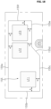
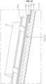
- FIGS. 1 to 27 illustrate examples of a display device according to embodiments of the present disclosure.
- a suffix such as “module” and “unit” may be used to refer to elements or components. Use of such a suffix herein is merely intended to facilitate description of the specification, and the suffix itself is not intended to give any special meaning or function.
- a display device 100 may include a display panel 110.
- the display panel 110 may display a screen.
- the display device 100 may include a first long side LS1, a second long side LS2 opposite the first long side LS1, a first short side SS1 adjacent to the first long side LS1 and the second long side LS2, and a second short side SS2 opposite the first short side SS1.
- first and second long sides LS1 and LS2 are greater than lengths of the first and second short sides SS1 and SS2.
- the lengths of the first and second long sides LS1 and LS2 may be substantially equal to the lengths of the first and second short sides SS1 and SS2.
- a direction parallel to the long sides LS1 and LS2 of the display device 100 may be referred to as a first direction DR1 or a left-and-right direction.
- a direction parallel to the short sides SS1 and SS2 of the display device 100 may be referred to as a second direction DR2 or an up-and-down direction.
- a direction perpendicular to the long sides LS1 and LS2 and the short sides SS1 and SS2 of the display device 100 may be referred to as a third direction DR3 or a front-and-rear direction.
- a direction in which the display device 100 displays an image may be referred to as a front (F, +z), and a direction opposite to the front may be referred to as a rear or back (R, -z).
- the second short side SS2 may be referred to as a left side (Le, -x).
- the first short side SS1 may be referred to as a right side (Ri, +x).
- the first long side LS1 may be referred to as an upper side (U, +y).
- the second short side LS2 may be referred to as a lower side (D, -y).
- the first long side LS1, the second long side LS2, the first short side SS1, and the second short side SS2 may be referred to as edges of the display device 100.
- points where the first short side LS1, the second long LS2, the first short side SS1, and the second short side SS2 meet one another may be referred to as corners.
- a point where the first short side SS1 and the first long side LS1 meet may be referred to as a first corner C1.
- a point where the first short side SS1 and the second long side LS2 meet may be referred to as a second corner C2.
- a point where the second short side SS2 and the second long side LS2 meet may be referred to as a third corner C3.
- a point where the second short side SS2 and the first long side LS1 meet may be referred to as a fourth corner C4.
- OLED organic light emitting diode
- the display panel 110 may define a front surface of the display device 100, and may display an image to the front.
- the display panel 110 may include a plurality of pixels to output the image while controlling color, brightness, and chroma of each pixel.
- the display panel 110 may be divided into an active area in which an image is displayed and a de-active area in which no image is displayed.
- the display panel 110 may generate light corresponding to a color of red, green, or blue in response to a control signal.
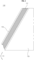
- a material complexed panel 130 may include a core 131, a front skin 132, and a rear skin 133.
- the core 131, the front skin 132, and the rear skin 133 may be coupled to each other.
- the material complexed panel 130 may be referred to as a fiber complexed panel 130, a fiber complexed plate 130, a material complexed plate 130, or a frame 130.
- the front skin 132 may define a front surface of the material complexed panel 130.
- the rear skin 133 may define a rear surface of the material complexed panel 130.
- the front skin 132 and the rear skin 133 may include a metal material.
- the front skin 132 and the rear skin 133 may include an aluminum (Al) material.
- the front skin 132 and the rear skin 133 may be a galvanized iron or galvanized steel sheet.
- the front skin 132 and the rear skin 133 may have a thickness of about 0.5 mm.
- the front skin 132 and the rear skin 133 may be disposed opposite each other with respect to the core 131.
- the core 131 may be disposed between the front skin 132 and the rear skin 133.
- the core 131 may include fibers.
- the core 131 may be formed of a composite material.
- the core 131 may include a main fiber and a binder fiber.
- the binder fiber may be mixed with the main fiber.
- a hot-melt sheet may be disposed between the front skin 132 and the core 131, and a hot-melt sheet may be disposed between the rear skin 133 and the core 131.
- the hot-melt sheet may be a film.
- the hot-melt sheet may be a film made of EVA, acrylic, polyurethane, or the like having a thickness of 50 micrometers or more.
- the core 131 and the hot-melt sheet may be roll laminated onto the front skin 132 and the rear skin 133 at a high temperature (e.g., 190 to 200 °C) for 1 minute or more.
- bending rigidity and/or torsional rigidity of the display device may be increased.
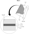
- the material complexed panel 130 may be manufactured by a process of pressing the front skin 132 and the rear skin 133 onto the core 131 using a plurality of rollers. Such a process may be referred to as Roll-to-Roll (R2R) processing.
- R2R Roll-to-Roll
- the front skin 132 may be unwound from a front drum Da
- the rear skin 133 may be unwound from a rear drum Db
- the core 131 may be moved by passing through a feeding roller Rd.
- a first adhesive 134a for coupling the front skin 132 to the core 131 may be unwound from a first drum Dc.
- a second adhesive 134b for coupling the rear skin 133 to the core 131 may be unwound from a second drum Db.
- the front skin 132, the first adhesive 134a, the core 131, the second adhesive 134b, and the rear skin 133 are stacked in this order, and may be guided toward an oven Ov by a guide roller Rc.
- the adhesive 134a, 134b may be a hot-melt sheet 134a, 134b.
- each of the front skin 132 and the rear skin 133 may be coupled to the core 131.
- the melting point of the first and second adhesives 134a and 134b may be about 150 °C
- the ambient temperature of the oven Ov may be about 200 °C.
- the peel-off force of the first and second adhesives 134a and 134b may be about 10 kgf or more.
- the front skin 132, the core 131, and the rear skin 133 that have passed through the oven Ov may be guided to a press roller Rb by the rotation of the pinch roller Ra, so as to be pressed by the press roller Rb. Accordingly, the coupling force among the front skin 132, the core 131, and the rear skin 133 may be further increased.
- the front skin 132, the core 131, and the rear skin 133, which are coupled to each other, may pass through the pinch roller Ra, and then may be cut by a cutter Ct to be manufactured as a material complexed panel 130 of a predetermined size.
- the press roller Rb or the pinch roller Ra may come into contact with an outer surface of each of the front skin 132 and the rear skin 133.
- the material complexed panel 130 may be moved in a longitudinal direction of the core 131.
- the front skin 132 and the rear skin 133 may be coupled to the core 131 sequentially from one end to the other end in the longitudinal direction of the core 131.
- the front skin 132 and the rear skin 133 of the material complexed panel 130 may be formed flat. That is, as a rear surface of the rear skin 133, which defines the rear surface of the display device 100, is formed flat, additional operations, such as painting the rear surface of the rear skin 133, attaching a sheet thereto, etc., for an aesthetically pleasing appearance may be performed easily.
- the flat rear skin 133 itself may define the rear surface of the display device 100.
- a process of sequentially stacking the front skin 132, the core 131, and the rear skin 133 followed by coupling the same may be used to manufacture the material complexed panel 130.
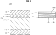
- the core 131 may include a main core 131a and a binder core 131b.
- the main core 131a may include a first fiber of a polyethylene terephthalate (PET) material and a second fiber of a long material (LM).
- PET polyethylene terephthalate
- LM long material
- the main core 131a may contain 50% of the first fiber and 50% of the second fiber.
- the binder core 131b may include an acrylic fiber.
- the front skin 132 may include an aluminum (Al) material or galvanized iron, and may be coupled to the binder core 131b by a first hot-melt adhesive 134a.
- the rear skin 133 may include an aluminum (Al) material or galvanized iron, and may be coupled to the main core 131a by a second hot-melt adhesive 134b.
- the front skin 132 may be located closer to the display panel 110 (see FIG. 16 ) compared to the rear skin 133, and may be exposed to a higher temperature than the rear skin 133. In other words, there may be a temperature difference between the front skin 132 and the rear skin 133. For example, the temperature difference between the front skin 132 and the rear skin 133 may be about 4 °C.
- the hot-melt adhesive 134a, 134b may consist of multi-layers of fiber materials (i.e., has a multilayered structure).
- the hot-melt adhesive 134a, 134b may include a first layer 1341, a second layer 1342, and a third layer 1343.
- the first layer 1341, the second layer 1342, and the third layer 1343 may each include a synthetic fiber material.
- the first layer 1341 may include a nylon material and may be disposed between the second layer 1342 and the third layer 1343.
- the second layer 1342 and the third layer 1343 may each include a polyurethane (PU) material.
- PU polyurethane
- elongation characteristics of each layer of the material complexed panel 130 may minimize warping caused by thermal deformation of the material complexed panel 130, which is due to a temperature difference between the front skin 132 and the rear skin 133.
- the material complexed panel 130 may include a flat part 130P, an outer part 135, and a receiving part 137.
- the front skin 132 of the material complexed panel 130 may define respective front surfaces of the flat part 130P, the outer part 135, and the receiving part 137.
- the outer part 135 may be formed around the flat part 130P.
- the outer part 135 may be formed by being pressed rearward from the flat part 130P.
- a first outer part 135a may be formed along an upper side of the flat part 130P.
- a second outer part 135b may be formed along a right side of the flat part 130P.
- a third outer part 135c may be formed along a lower side of the flat part 130P.
- a fourth outer part 135d may be formed along a left side of the flat part 130P.
- the receiving part 137 may be formed between the flat part 130P and the third outer part 135c.
- the receiving part 137 may be formed by being pressed rearward from the flat part 130P and/or the third outer part 135c.
- a cable hole 136 may be formed through the receiving part 137 in the front-and-rear direction.
- a plurality of cables holes 136a and 136b may be adjacent to each other.
- a thickness T1 of the flat part 130P may be greater than a thickness T2 of the receiving part 137.
- a step D1 between the front skin 132 of the flat part 130P and the front skin 132 of the receiving part 137 may be greater than a step D2 between the rear skin 133 of the flat part 130P and the rear skin 133 of the receiving part 137.
- a thickness T4 of the third outer part 135c may be greater than the thickness T2 of the receiving part 137.
- a step D2 between the rear skin 133 of the third outer part 135c and the rear skin 133 of the receiving part 137 may be equal to the step D2 between the rear skin 133 of the flat part 130P and the rear skin 133 of the receiving part 137.
- a protruding pad 138 may protrude forward from the front skin 132 of the third outer part 135c.
- a thickness T3 of the protruding pad 138 may be greater than the thickness T4 of the third outer part 135c, may be greater than the thickness T2 of the receiving part 137, and may be less than the thickness T1 of the flat part 130P.
- a step D4 between the front skin 132 of the protruding pad 138 and the front skin 132 of the third outer part 135c may be less than the step D1, the step D2, and a step D3.
- the step D3 descending from the front skin 132 of the protruding pad 138 to the front skin 132 of the receiving part 137 may be less than the step D1 and greater than the step D2.
- a side frame 140 may extend along the perimeter or periphery of the material complexed panel 130.
- the side frame 140 may be coupled to the front skin 132 of the outer part 135 (see FIG. 6 ) of the material complexed panel 130 by a hot-melt adhesive 130H.
- the side frame 140 may include a metal material such as aluminum (Al).
- the side frame 140 may be referred to as a guide panel 140 or a middle cabinet 140.
- the side frame 140 may include a vertical portion 140V and a horizontal portion 140H.
- the vertical portion 140V may extend in the front-and-rear direction, and may cover a side surface of the material complexed panel 130.
- the horizontal portion 140H may extend from the vertical portion 140V in a direction intersecting the vertical portion 140V, and may be positioned at the front of the outer part 135.
- the outer part 135 may be formed by being pressed rearward from the front skin 132 of the flat part 130P.
- restriking may be performed to flatten the outer part 135.
- a thickness T1 of the flat part 130P may be 4.0 mm
- a thickness T4 of the outer part 135 may be 3.0 mm.
- the hot-melt adhesive 130H may be applied onto the outer part 135, and may be disposed between the outer part 135 and the horizontal portion 140H.
- a horn UW of an ultrasonic welder may be placed on a front surface of the vertical portion 140H, so as to apply ultrasonic vibration to the vertical portion 140H and hot-melt adhesive 130H.
- the horizontal portion 140H may be ultrasonic welded to the outer part 135 through the hot-melt adhesive 130H.
- the front skin 132 of the outer part 135 may be pressed toward the rear skin 133 by the horn UW, and accordingly, a thickness T5 of the outer part 135 may be reduced.
- the thickness T5 of the outer part 135 may be 2.4 to 2.5 mm.
- a pressed amount (D6-D5) of the outer part 135 by the horn UW may be 0.5 to 0.6 mm. Since the outer part 135 is pressed during the ultrasonic welding described above, namely, under high temperature, the outer part 135 may retain its shape without spring back.
- a sum T10a of the thickness T5 of the outer part 135, a thickness of the hot-melt adhesive 130H, and a thickness T10 of the horizontal portion 140H may be less than the thickness T1 of the flat part 130P.
- the thickness T1 of the flat part 130P may be 4.0 mm.
- the thickness T5 of the outer part 135 may be 2.4 to 2.5 mm
- the thickness of the hot-melt adhesive 130H may be 0.1 mm
- the thickness T10 of the horizontal portion 140H may be 1.1 mm, and therefore the sum T10a of them may be 3.6 to 3.7 mm.
- the display panel 110 may be positioned at the front of the horizontal portion 140H.
- a first adhesive member AD1 may be disposed between the front skin 132 of the flat part 130P and a rear surface of the display panel 110, and may be coupled to the flat part 130P and the display panel 110.
- the first adhesive member AD1 may have a thickness T11 of 0.5 mm.
- a second adhesive member AD2 may be disposed between a front surface of the horizontal portion 140H and the rear surface of the display panel 110, and may be coupled to the horizontal portion 140H and the display panel 110.
- the second adhesive member AD2 may have a thickness T12 of 0.8 to 0.9 mm.
- the adhesive member AD1, AD2 may be a double-sided tape.
- the display panel 110 may be coupled to the material complexed panel 130 and the side frame 140, and may be positioned flat with respect to the material complexed panel 130.
- the vertical portion 140V may cover a side surface of the display panel 110.
- the side frame 140 may include a first part 141, a second part 142, a third part 143, a fourth part 144, and a fifth part 145.
- the first part 141 may extend along the first outer part 135a (see FIG. 6 ), and may include a first horizontal portion 141H (see FIG. 8 ) and a first vertical portion 141V (see FIG. 8 ).
- the first horizontal portion 141H may be parallel to the first outer part 135a, and may be fixed on the first outer part 135a by the hot-melt adhesive 130H.
- the first vertical portion 141V may intersect the first horizontal portion 141H, and may cover an upper side of the material complexed panel 130.
- the second part 142 may be bent downward at a right end of the first part 141 (see a first corner C1), and may include a second horizontal portion 142H and a second vertical portion 142V.
- the second horizontal portion 142H may be parallel to the second outer part 135b, and may be fixed on the second outer part 135b by the hot-melt adhesive 130H.
- the second vertical portion 142V may intersect the second horizontal portion 142H, and may cover a right side of the material complexed panel 130.
- the third part 143 may be bent leftward at a lower end of the second part 142 (see a second corner C2), and may include a third horizontal portion 143H (see FIG. 14 ) and a third vertical portion 143V (see FIG. 14 ).
- the third horizontal portion 143H may be parallel to the third outer part 135c, and may be fixed on the third outer part 135c by the hot-melt adhesive 130H.
- the third vertical portion 143V may intersect the third horizontal portion 143H, and may cover a lower side of the material complexed panel 130.
- the fourth part 144 may be aligned to the third part 143 along the third outer part 135c, and an end of the fourth part 144 may be connected to an end of the third part 143.
- the fourth part 144 may include a fourth horizontal portion 144H (see FIG. 15 ) and a fourth vertical portion 144V (see FIG. 15 ).
- the fourth horizontal portion 144H may be parallel to the third outer part 135c, and may be fixed on the third outer part 135c by the hot-melt adhesive 130H.
- the fourth vertical portion 144V may interest the fourth horizontal portion 144H, and may cover the lower side of the material complexed panel 130.
- the fifth part 145 may be bent downward at a left end of the first part 141 (see a fourth corner C4), and the fourth part 144 may be bent rightward at a lower end of the fifth part 145 (see a third corner C3).
- the fifth part 145 may include a fifth horizontal portion (not shown) and a fifth vertical portion (not shown).
- the fifth horizontal portion (not shown) may be parallel to the fourth outer part 135d, and may be fixed on the fourth outer part 135d by the hot-melt adhesive 130H.
- the fifth vertical portion (not shown) may intersect the fifth horizontal portion (not shown), and may cover a left side of the material complexed panel 130.
- a gap G1 may be formed between the first horizontal portion 141H of the first part 141 and the second horizontal portion 142H of the second part 142.
- the first vertical portion 141V of the first part 141 and the second vertical portion 142V of the second part 142 may be connected while being bent.
- a hole H1 may be adjacent to the vertical portions 141V and 142V, may be connected to the gap G1, and may have a larger diameter than the gap G1.
- a gap like the gap G1 may be formed between the first horizontal portion 141H of the first part 141H and the fifth horizontal portion (not shown) of the fifth part 145 (see FIG. 12 ).
- the first vertical portion 141V of the first part 141 and the fifth vertical portion (not shown) of the fifth part 145 may be connected while being bent.
- a hole like the hole H1 may be adjacent to the first vertical portion 141V and the fifth vertical portion (not shown).
- a gap G3 may be formed between the second horizontal portion 142H of the second part 142 and the third horizontal portion 143H of the third part 143.
- the second vertical portion 142V of the second part 142 and the third vertical portion 143V of the third part 143 may be connected while being bent.
- a hole H3 may be adjacent to the vertical portions 142V and 143V, may be connected to the gap G3, and may have a larger diameter than the gap G3.
- a gap like the gap G3 may be formed between the fifth horizontal portion (not shown) of the fifth part 145 (see FIG. 12 ) and the fourth horizontal portion 144H (see FIG. 15 ) of the fourth part 144 (see FIG. 12 ).
- the fifth vertical portion (not shown) of the fifth part 145 and the fourth vertical portion 144V (see FIG. 15 ) of the fourth part 144 may be connected while being bent.
- a hole like the hole H3 may be adjacent to the fifth vertical portion (not shown) and the fourth vertical portion 144V.
- a corner 130C1 adjacent to the first corner C1 of the flat part 130P may be rounded.
- a radius of curvature of the corner 130C1 may be 10 mm.
- a corner adjacent to the fourth corner C4 (see FIG. 12 ) of the flat part 130P may be rounded like the corner 130C1.
- a corner 130C2 adjacent to the second corner C2 of the flat part 130P may be rounded.
- a radius of curvature of the corner 130C2 may be 10 mm.
- a corner adjacent to the third corner C3 (see FIG. 12 ) of the flat part 130P may be rounded like the corner 130C2.
- the third horizontal portion 143H of the third part 143 may be in contact with the fourth horizontal portion 144H of the fourth part 144.
- the third vertical portion 143V of the third part 143 may be in contact with the fourth vertical portion 144V of the fourth part 144.
- An end of the third part 143 may be connected to an end of the fourth part 144.
- the end of the third part 143 may be welded to the end of the fourth part 144.
- the display panel 110 may be coupled or fixed on the side frame 140.
- the horizontal portion 143H of the side frame 140 may support the rear surface of the display panel 110, and the vertical portion 143V of the side frame 140 may cover the side surface of the display panel 110.
- the vertical portion 143V of the third part 143 of the side frame 140 may cover a lower side surface of the display panel 110.
- the vertical portion 143V may cover a side surface of the material complexed panel 130.
- the vertical portion 143V of the third part 143 of the side frame 140 may cover a side surface of the third outer part 135c of the material complexed panel 130.
- a flexible cable 113 may extend from a lower side of the display panel 110 to a region between the display panel 110 and the horizontal portion 143H of the side frame 140.
- the flexible cable 113 may extend between the rear surface of the display panel 110 and the material complexed panel 130.
- the flexible cable 113 may be a COF 113.
- a source signal substrate 115 may be electrically connected to the flexible cable 113.
- the source signal substrate 115 may be fixed to one surface of the flexible cable 113.
- the source signal substrate 115 may be an S-PCB 115.
- the source signal substrate 115 may be positioned in the receiving part 137 of the material complexed panel 130.
- the flexible cable 113 may be positioned between the protruding pad 130 of the material complexed panel 130 and the display panel 110.
- the flexible cable 113 may be in contact with the protruding pad 130. Heat generated in the source signal substrate 115 and/or the flexible cable 113 may be dissipated through the protruding pad 138.
- a heat dissipation pad 114 may be positioned between the flexible cable 113, which is in contact with the protruding pad 138, and the rear surface of the display panel 110.
- the heat dissipation pad 114 may include an elastic material 114a and a conductive film 114b.
- the core 114a of the heat dissipation pad 114 may be formed of an elastic material, and the conductive film 114b may cover the core 114a of the heat dissipation pad 114. Accordingly, the flexible cable 113 may be maintained in contact with the protruding pad 138.
- a PCB plate 150 may be coupled to the rear of the material complexed panel 130.
- the PCB plate 150 may be referred to as a rear plate 150.
- the rear plate 150 may be fixed to the rear surface of the material complexed panel 130.
- the rear plate 150 may include a metal.
- the rear plate 150 may be made of electrolytic galvanized iron (EGI).
- EGI electrolytic galvanized iron
- the rear plate 150 may have a thickness of about 0.5 mm.
- the electrical conductivity of the rear plate 150 may be less than or equal to 1 ⁇ 10 7 (units omitted).
- a curve may be formed as the rear plate 150 is pressed.
- the press processed rear plate 150 may have increased rigidity.
- the rear plate 150 may include a flat part 153 and a frame part 151,152.
- a first part 151 of the frame part (151,152) may define an outer edge or periphery of the rear plate 150.
- the first part 151 may include a first horizontal part 151a, a second horizontal part 151c, a first vertical part 151b, and a second vertical part 151d.
- a second part 152 of the frame part (151,152) may be connected to the first part 151, and may form a curve recessed or protruding from the flat part 153 while crossing the flat part 153.
- the second part 152 may include a first vertical part 152a, a second vertical part 152b, a first horizontal part 152c, and a second horizontal part 152d.
- the frame part 151,152 may allow bending rigidity and/or torsional rigidity of the rear plate 150 to be increased.
- the flat part 153 may include a first side part 153a, a center part 153b, and a second side part 153c.
- a power supply unit PSU (see FIG. 25 ) may be mounted or fixed on the first side part 153a.
- a main board MB may be mounted or fixed on the second side part 153c.
- a T-CON board TB may be mounted or fixed to the center part 153b.
- a speaker assembly SPK may be mounted or fixed to a first lower part 153d and/or a second lower part 153e.
- An opened portion or opening 155 may be formed in the first side part 153a.
- the opening 155 may be referred to as a cut-out portion 155.
- the opening 155 may include a first line 155a, a second line 155b, a third line 155c, a fourth line 155d, a fifth line 155e, and/or a sixth line 155f.
- a line filter (LF1, LF2, LF3) of the power supply unit PSU (see FIG. 25 ) may be positioned between the lines 155a, 155b, 155c, 155d, 155e, and 155f of the opening 155.
- a plurality line filters LF1, LF2, and LF3 may be provided.
- the first line 155a may form a long side.
- the third line 155c may face the first line 155a, and may be shorter than the first line 155a.
- the fifth line 155e may face the first line 155a, and may be shorter than the first line 155a and/or the third line 155c.
- the fifth line 155e may be parallel to the third line 155c.
- a distance between the third line 155c and the first line 155a may be greater than a distance between the fifth line 155e and the first line 155a.
- the second line 155b may form a short side and may connect the first line 155a and the third line 155c
- the sixth line 155f may form a short side and may connect the first line 155a and the fifth line 155e.
- a length of the second line 155b may be greater than a length of the sixth line 155f.
- the sixth line 155f may face the second line 155b.
- the fourth line 155d may connect the third line 155c and the fifth line 155e.
- the fourth line 155d may be inclined with respect to the third line 155c.
- the fourth line 155d may be inclined with respect to the fifth line 155e.
- a first line filter LF1 may be positioned between the first line 155a and the third line 155c.
- a second line filter LF2 may be positioned between the first line 155a and the fourth line 155d and/or the fifth line 155e.
- a third line filter LF3 may be positioned between the first line 155a and the fifth line 155e.
- the line filter LF (LF1, LF2, LF3) may be spaced apart from the lines 155a, 155b, 155c, 155d, 155e, and 155f of the opening 155 by a predetermined distance or more.
- the line filter LF may be spaced apart from the lines 155a, 155b, 155c, 155d, 155e, and 155f of the opening 155 by a first distance A or more.
- the first line filter LF1 may be spaced apart from the second line 155b and/or the third line 155c by the first distance A or more.
- the second line filter LF2 may be spaced apart from the first line 155a and/or the fifth line 155e by the first distance A or more.
- the third line filter LF3 may be spaced apart from the first line 155a and/or the fifth line 155e by the first distance A or more, while being spaced apart from the sixth line 155f by the first distance A or more.
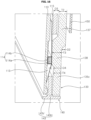
- the power supply unit PSU may be spaced apart from the material complexed panel 130 and the rear plate 15, and may be mounted or fixed to a rear surface of the rear plate 150.
- the power supply unit PSU may include the line filter LF.
- the line filter LF may include a coil and may remove noise from the power supply.
- An electromagnetic field may be formed around the line filter LF.
- the electromagnetic field generated when the line filter LF is operated may cause the rear plate 150 to vibrate.
- the vibration of the rear plate 150 may be transmitted to the material complexed panel 130 to thereby generate vibration and/or noise.
- a current value of the line filter LF may increase, thereby increasing the magnitude of an electromagnetic field generated by the line filter LF.
- vibration of the rear plate 150 may increase with a decrease in distance from the line filter LF, while vibration of the rear plate 150 may decrease with an increase in distance from the line filter LF.
- the opening 155 of the rear plate 150 that corresponds to the line filter LF may prevent the rear plate 150 from vibrating caused by the line filter LF.
- the opening 155 of the rear plate 150 which is formed to secure the distance between the line filter LF and the rear plate 150, increases in size, the rigidity of the rear plate 150 may be reduced. Therefore, the distance of the rear plate 150 formed by the line filter LF and the opening 155 may not only affect the rigidity of the rear plate 150 but also noise and/or vibration generated in the rear plate 150.
- a current flowing through the line filter LF may be 3.5A to 4.3A
- a second distance B from the line filter LF to the rear plate 150 may be 7 to 8 mm
- a first distance A from the line filter LF to an edge of the opening 155 of the rear plate 150 may be 15 mm or more.
- a back cover 180 may cover the power supply unit PSU and/or the line filter LF.
- the back cover 180 may be coupled to the rear plate 150 or the material complexed panel 130.
- the back cover 180 may include a synthetic resin.
- An insulation sheet 170 and/or a heat dissipation sheet 170 may be disposed between the power supply unit PSU and the back cover 180, and may be attached to the back cover 180.
- the insulation sheet 170 and/or the heat dissipation sheet 170 may have an opening, and the line filter LF may be aligned to the opening.
- the heat dissipation sheet 170 may be a graphite sheet.
- a first opening 155 may include a first line 155a, a second line 155b, a third line 155c, a fourth line 155d, a fifth line 155e, and/or a sixth line 155f.
- a second opening 157 may be disposed adjacent to the first opening 155.
- a line filter LF1, LF2 of the power supply unit PSU may be disposed inside the first opening 155 between the lines 155a, 155b, 155c, 155d, 155e, and 155f of the first opening 155.
- a line filter LF3 may be disposed in the second opening 157.
- the first line 155a may form a long side.
- the third line 155c may face the first line 155a, and may be shorter than the first line 155a.
- the fifth line 155e may face the first line 155a, and may be shorter than the first line 155a and/or the third line 155c.
- the fifth line 155e may be parallel to the third line 155c.
- a distance between the third line 155c and the first line 155a may be less than a distance between the fifth line 155e and the first line 155a.
- the second line 155b may form a short side and may connect the first line 155a and the third line 155c, and the sixth line 155f may form a short side and may connect the first line 155a and the fifth line 155e.
- a length of the second line 155b may be less than a length of the sixth line 155f.
- the sixth line 155f may face the second line 155b.
- the fourth line 155d may connect the
- a first line filter LF1 may be positioned between the first line 155a and the third line 155c. Also, the first line filter LF1 may be spaced apart from the second line 155b.
- a second line filter LF2 may be positioned between the first line 155a and the fifth line 155e. Also, the second line filter LF2 may be spaced apart from the fourth line 155d and/or the sixth line 155f.
- a third line filter LF3 may be positioned in the second opening 157. The third line filter LF3 may be spaced apart from edges of the second opening 157.
- the line filters LF1 and LF2 may be spaced apart from the lines 155a, 155b, 155c, 155d, 155e, and 155f of the first opening 155 or the edges of the second opening 157.
- the line filters LF1 and LF2 may be spaced apart from the lines 155a, 155b, 155c, 155d, 155e, and 155f of the first opening 155 by a first distance A or more.
- the first line filter LF1 may be spaced apart from the first line 155a, the second line 155b, and/or the third line 155c by the first distance A or more.
- the second line filter LF2 may be spaced apart from the fourth line 155d, the fifth line 155e, and/or the sixth line 155f by the first distance A or more.
- the third line filter LF3 may be spaced apart from the edges of the second opening 157 by the first distance A or more.
- the power supply unit PSU may be spaced apart from the material complexed panel 130 and the rear plate 150, and may be mounted or fixed to a rear surface of the rear plate 150.
- the power supply unit PSU may include the line filter LF.
- the line filter LF may include a coil and may remove noise from the power supply.
- An electromagnetic field may be formed around the line filter LF.
- the electromagnetic field generated when the line filter LF is operated may cause the rear plate 150 to vibrate.
- the vibration of the rear plate 150 may be transmitted to the material complexed panel 130 to thereby generate vibration and/or noise.
- a current value of the line filter LF may increase, thereby increasing the magnitude of an electromagnetic field generated by the line filter LF.
- vibration of the rear plate 150 may increase with a decrease in distance from the line filter LF, while vibration of the rear plate 150 may decrease with an increase in distance from the line filter LF.
- the opening 155, 157 of the rear plate 150 that corresponds to the line filter LF may prevent the rear plate 150 from vibrating caused by the line filter LF.
- the opening 155 of the rear plate 150 which is formed to secure the distance between the line filter LF and the rear plate 150, increases in size, the rigidity of the rear plate 150 may be reduced. Therefore, the distance of the rear plate 150 formed by the line filter LF and the opening 155 may not only affect the rigidity of the rear plate 150 but also noise and/or vibration generated in the rear plate 150.
- a current flowing through the line filter LF may be 2.8A to 3.2A
- a second distance B from the line filter LF to the rear plate 150 may be 7 to 8 mm
- a first distance A from the line filter LF to an edge of the first opening 155 and/or the second opening 157 of the rear plate 150 may be 10 mm or more.
- the opening 155 may include a first line 155a, a second line 155b, a third line 155c, a fourth line 155d, a fifth line 155e, and/or a sixth line 155f.
- a line filter (LF1, LF2, LF3, LF4, LF5) of the power supply unit PSU may be positioned between the lines 155a, 155b, 155c, 155d, 155e, and 155f of the opening 155.
- a plurality of line filters LF1, LF2, LF3, LF4, and LF5 may be provided.
- the first line 155a may form a short side.
- the third line 155c may face the first line 155a and may be longer than the first line 155a.
- the second line 155b may form a long side and may connect the first line 155a and the third line 155c, and the fourth line 155d may form a long side and may connect the first line 155a and the third line 155c.
- the fifth line 155e may face the second line 155b, and may be shorter than the first line 155a and/or the third line 155c.
- the fifth line 155e may be parallel to the fourth line 155d.
- the fifth line 155e may protrude from a portion of the fourth line 155d.
- a distance from the second line 155b to the fifth line 155e may be less than a distance from the second line 155b to the fourth line 155d.
- a length of the fifth line 155e may be greater than a length of the sixth line 155f.
- the sixth line 155f may face the second line 155b.
- the sixth line 155f may connect the first line 155a and the fourth line 155d.
- a first line filter LF1 may be positioned adjacent to a corner defined by the first line 155a and the second line 155b.
- a second line filter LF2 may be positioned adjacent to a corner defined by the first line 155a and the sixth line 155f, and may be positioned between the first line filter LF1 and the fourth line 155d.
- a third line filter LF3 may be positioned between the second line 155b and the fourth line 155d.
- a fourth line filter LF4 may be positioned between the second line 155b and the fifth line 155e.
- a fifth line filter LF5 may be positioned adjacent to a corner defined by the third line 155c and the fourth line 155d, between the second line 155b and the fourth line 155d.
- the line filter LF (LF1, LF2, LF3, LF4, LF5) may be spaced apart from the lines 155a, 155b, 155c, 155d, 155e, and 155f of the opening 155 by a predetermined distance or more.
- the line filter LF may be spaced apart from the lines 155a, 155b, 155c, 155d, 155e, and 155f of the opening 155 by a first distance A or more.
- the first line filter LF1 may be spaced apart from the first line 155a and/or the second line 155b by the first distance A or more.
- the second line filter LF2 may be spaced apart from the fourth line 155d and/or the sixth line 155f by the first distance A or more.
- the third line filter LF3 may be spaced apart from the fourth line 155d and/or the fifth line 155e by the first distance A or more.
- the fourth line filter LF4 may be spaced apart from the fifth line 155e by the first distance A or more.
- the fifth line filter LF5 may be spaced apart from the fourth line 155d and/or the third line 155c by the first distance A or more.
- the power supply unit PSU may be spaced apart from the material complexed panel 130 and the rear plate 150, and may be mounted or fixed to a rear surface of the rear plate 150.
- the power supply unit PSU may include the line filter LF.
- the line filter LF may include a coil and may remove noise from the power supply.
- An electromagnetic field may be formed around the line filter LF.
- the electromagnetic field generated when the line filter LF is operated may cause the rear plate 150 to vibrate.
- the vibration of the rear plate 150 may be transmitted to the material complexed panel 130 to thereby generate vibration and/or noise.
- a current value of the line filter LF may increase, thereby increasing the magnitude of an electromagnetic field generated by the line filter LF.
- vibration of the rear plate 150 may increase with a decrease in distance from the line filter LF, while vibration of the rear plate 150 may decrease with an increase in distance from the line filter LF.
- the opening 155 of the rear plate 150 that corresponds to the line filter LF may prevent the rear plate 150 from vibrating caused by the line filter LF.
- the opening 155 of the rear plate 150 which is formed to secure the distance between the line filter LF and the rear plate 150, increases in size, the rigidity of the rear plate 150 may be reduced. Therefore, the distance of the rear plate 150 formed by the line filter LF and the opening 155 may not only affect the rigidity of the rear plate 150 but also noise and/or vibration generated in the rear plate 150.
- a current flowing through the line filter LF may be 5A to 5.4A
- a second distance B from the line filter LF to the rear plate 150 may be 7 to 8 mm
- a first distance A from the line filter LF to an edge of the opening 155 of the rear plate 150 may be 20 mm or more.
- the side frame 140 may be coupled to the rear of the material complexed panel 130.
- the side frame 140 may be coupled to the rear surface of the material complexed panel 130 by an adhesive member AD.
- the rear plate 150 may be coupled or fixed to the rear surface of the material complexed panel 130.
- a first heat dissipation sheet 161 may be coupled or attached to the first side part 153a.
- the first heat dissipation sheet 161 may be a graphite sheet.
- the first heat dissipation sheet 161 may be an aluminum sheet.
- the first heat dissipation sheet 161 may cover the opening 155 (see FIG. 17 ).
- the first heat dissipation sheet 161 may dissipate heat generated in the power supply unit PSU (see FIG. 26 ).
- a second heat dissipation sheet 162 may be coupled or attached to the center part 153b.
- the second heat dissipation sheet 162 may be a graphite sheet.
- the second heat dissipation sheet 162 may be an aluminum sheet.
- the second heat dissipation sheet 162 may dissipate heat generated in the T-CON board TB.
- a first insulation sheet 163 may be coupled or attached to the first side part 153a.
- the first insulation sheet 163 may cover the first heat dissipation sheet 161.
- the first insulation sheet 163 may be attached to the first heat dissipation sheet 161.
- a second insulation sheet 165 may be coupled or attached to the center part 153b.
- the second insulation sheet 165 may cover the second heat dissipation sheet 162.
- the second insulation sheet 165 may be attached to the second heat dissipation sheet 162.
- a third insulation sheet 164 may be coupled or attached to the second side part 153c.
- the power supply unit PSU may be positioned on the first heat dissipation sheet 161 and/or the first heat dissipation sheet 163, and may be coupled or fixed to the first side part 153a.
- the T-CON board TB may be positioned on the second heat dissipation sheet 162 and/or the second insulation sheet 165, and may be coupled or fixed to the center part 153b.
- the main board MB may be positioned on the third insulation sheet 164, and may be coupled or fixed to the second side part 153c.
- the speaker assembly SPK may be mounted or fixed to the first lower part 153d and/or the second lower part 153e.
- the display panel 110 may be positioned at the front of the material complexed panel 130.
- the display panel 110 may be coupled or fixed to the front surface of the material complexed panel 130.
- the display panel 110 may form a predetermined gap with the material complexed panel 130.
- the skin 132, 133 (see FIG. 2 ) of the material complexed panel 130 may include aluminum.
- the rear plate 150 may be positioned at the rear of the material complexed panel 130.
- the rear plate 150 may be coupled or fixed to the rear surface of the material complexed panel 130.
- the rear plate 150 may be disposed opposite the display panel 110 with respect to the material complexed panel 130.
- the rear plate 150 may be made of electrolytic galvanized iron (EGI).
- the opening 155, 157 may be formed in the rear plate 150.
- the opening 155, 157 may be formed by cutting out a portion of the rear plate 150.
- the heat dissipation sheet 161 may cover the opening 155, 157 of the rear plate 150.
- the heat dissipation sheet 161 may be a graphite sheet.
- the insulation sheet 163 may cover the rear of the opening 155, 157 of the rear plate 150 while covering the heat dissipation sheet 161.
- the heat dissipation sheet 163 may be fixed or attached to the rear surface of the rear plate 150.
- the power supply unit PSU may be positioned at the rear of the heat dissipation sheet 161 and/or the insulation sheet 163, and may be coupled or fixed to the rear plate 150.
- the power supply unit PSU may include the line filter LF.
- the opening 155, 157 of the rear plate 150 may be aligned to the line filter LF.
- AC power may be supplied to the power supply unit PSU.
- the power supply unit PSU may convert AC power into DC power.
- the line filter LF may include a coil.
- the line filter LF may generate an electromagnetic field.
- the electromagnetic field generated by the line filter LF may cause the rear plate 150 (e.g., steel plate) to vibrate. As the rear plate 150 vibrates, it may cause noise to the material complexed panel 130.
- the opening 157, 159 may prevent the rear plate 150 from vibrating caused by the line filter LF.
- a display device includes: a display panel; a frame to which the display panel is coupled; a rear plate disposed opposite the display panel with respect to the frame, the rear plate being coupled to the frame; and a power supply unit fixed to the rear plate and comprising a line filter.
- the rear plate may have an opening aligned to the line filter of the power supply unit.
- the rear plate may include iron.
- a size of the opening may be greater than a size of the line filter.
- the display device may further include a heat dissipation sheet disposed between the line filter and the rear plate, the heat dissipation sheet covering the opening and being supported on the rear plate.
- the heat dissipation sheet may include a graphite sheet.
- the display device may further include an insulation sheet disposed between the line filter and the heat dissipation sheet, the insulation sheet covering the heat dissipation sheet and being supported on the rear plate.
- the line filter may be provided in plurality.
- the opening may include: a first opening that corresponds to at least one line filter of the plurality of line filters; and a second opening that corresponds to a remaining line filter of the plurality of line filters.
- the opening may include an edge that defines a perimeter of the opening. On a plane defined by the opening, a distance from a periphery of the line filter to the edge may be 15 mm or more.
- a distance from the opening to the line filter may be 7 to 8 mm.
- the opening may include: a first line that forms one edge of the opening; and a second line that forms another edge of the opening.
- the line filter may be located closer to the first line than the second line.
- a distance from a periphery of the line filter to the first line may be 15 mm or more.
- a distance from the opening to the line filter may be 7 to 8 mm.
- the frame may include: a front skin facing the display panel; a rear skin facing the front skin; and a core including a fiber, the core being disposed between the front skin and the rear skin.
- the rear skin may include aluminum.
- a configuration "A” described in one embodiment of the disclosure and the drawings, and a configuration "B” described in another embodiment of the disclosure and the drawings may be combined with each other. Namely, although the combination between the configurations is not directly described, the combination is possible except in the case where it is described that the combination is impossible.
Landscapes
- Physics & Mathematics (AREA)
- Engineering & Computer Science (AREA)
- General Physics & Mathematics (AREA)
- Nonlinear Science (AREA)
- Theoretical Computer Science (AREA)
- Crystallography & Structural Chemistry (AREA)
- Optics & Photonics (AREA)
- Chemical & Material Sciences (AREA)
- Microelectronics & Electronic Packaging (AREA)
- Mathematical Physics (AREA)
- General Engineering & Computer Science (AREA)
- Computer Hardware Design (AREA)
- Human Computer Interaction (AREA)
- Devices For Indicating Variable Information By Combining Individual Elements (AREA)
- Electroluminescent Light Sources (AREA)
Abstract
A display device is disclosed. The display device includes: a display panel; a frame to which the display panel is coupled; a rear plate disposed opposite the display panel with respect to the frame, the rear plate being coupled to the frame; and a power supply unit fixed to the rear plate and including a line filter, wherein the rear plate has an opening aligned to the line filter of the power supply unit.
Description
- The present disclosure relates to a display device.
- With the development of information society, there has been a growing demand for various types of display devices. In order to meet such demand, various display devices, such as a liquid crystal display (LCD), a plasma display panel (PDP), an electro luminescent display (ELD), a vacuum fluorescent display (VFD), an organic light emitting diode (OLED), and the like, have been developed and used.
- Among them, an LCD panel includes a TFT substrate and a color substrate that are disposed opposite each other with a liquid crystal layer interposed therebetween, and can display an image using light provided from a backlight unit. In addition, an OLED panel can display an image by depositing an organic material layer capable of emitting light by itself on a substrate on which a transparent electrode is formed.
- In particular, a display device using an organic light emitting diode (OLED) has excellent luminance and viewing angle characteristics compared to a liquid crystal display, and requires no backlight unit, which is advantageous in that the OLED display device can be implemented as an ultra-thin display device.
- Recently, a lot of research has been conducted on an ultra-thin large screen display device.
- It is an objective of the present disclosure to solve the above and other problems.
- It is another objective of the present disclosure to achieve structural rigidity of an ultra-thin large screen display device.
- It is yet another objective of the present disclosure to provide a display device that can suppress or reduce noise/vibration that may be generated in an electromagnetic structure.
- It is yet another objective of the present disclosure to provide a display device that can suppress or reduce noise/vibration caused by a spatial limitation of an ultra-thin large screen display device.
- According to an aspect of the subject matter described in this application, a display device includes: a display panel; a frame to which the display panel is coupled; a rear plate disposed opposite the display panel with respect to the frame, the rear plate being coupled to the frame; and a power supply unit fixed to the rear plate and including a line filter, wherein the rear plate has an opening aligned to the line filter of the power supply unit.
- A display device according to the present disclosure has the following effects.
- According to least one of the embodiments of the present disclosure, it is possible to achieve structural rigidity of an ultra-thin large screen display device.
- According to least one of the embodiments of the present disclosure, it is possible to provide a display device capable of suppressing or reducing noise/vibration that may be generated in an electromagnetic structure.
- According to least one of the embodiments of the present disclosure, it is possible to provide a display device capable of suppressing or reducing noise/vibration caused by a spatial limitation of an ultra-thin large screen display device.
- Further scope of applicability of the present disclosure will become apparent from the following detailed description. However, it should be understood that the detailed description and specific embodiments such as preferred embodiments of the present disclosure are given by way of example only, since various changes and modifications within the idea and scope of the present disclosure may be clearly understood by those skilled in the art.
-
FIGS. 1 to 27 illustrate examples of a display device according to embodiments of the present disclosure. - Description will now be given in detail according to exemplary embodiments disclosed herein, with reference to the accompanying drawings. For the sake of brief description with reference to the drawings, the same or equivalent components may be denoted by the same reference numbers, and description thereof will not be repeated.
- In the following description, a suffix such as "module" and "unit" may be used to refer to elements or components. Use of such a suffix herein is merely intended to facilitate description of the specification, and the suffix itself is not intended to give any special meaning or function.
- In the present disclosure, that which is well known to one of ordinary skill in the relevant art has generally been omitted for the sake of brevity. The accompanying drawings are used to help easily understand the technical idea of the present disclosure and it should be understood that the idea of the present disclosure is not limited by the accompanying drawings. The idea of the present disclosure should be construed to extend to any alterations, equivalents, and substitutes besides the accompanying drawings.
- It will be understood that although the terms "first", "second", etc. may be used herein to describe various elements, these elements should not be limited by these terms. These terms are only used to distinguish one element from another.
- It will be understood that when a component is referred to as being "connected to" or "coupled to" another component, it may be directly connected to or coupled to another component, or intervening components may be present. In contrast, when a component is referred to as being "directly connected to" or "directly coupled to" another component, there are no intervening components present.
- As used herein, a singular representation is intended to include a plural representation unless the context clearly indicates otherwise.
- It will be understood that the terms "comprises" and/or "has," when used in this specification, specify the presence of a stated feature, number, step, operation, component, element, or combination thereof, but do not preclude the presence or addition of one or more other features, numbers, steps, operations, components, elements, or combinations thereof.
- The directions "up (U)", "down (D)", "left (Le)", "right (Ri)", "front (F)", and "rear (R)" shown in the drawings are only for the convenience of description, and the technical concept disclosed in the specification is not limited by these directions.
- Referring to
FIG. 1 , adisplay device 100 may include adisplay panel 110. Thedisplay panel 110 may display a screen. - The
display device 100 may include a first long side LS1, a second long side LS2 opposite the first long side LS1, a first short side SS1 adjacent to the first long side LS1 and the second long side LS2, and a second short side SS2 opposite the first short side SS1. For the convenience of explanation, it is illustrated and described that lengths of the first and second long sides LS1 and LS2 are greater than lengths of the first and second short sides SS1 and SS2. However, the lengths of the first and second long sides LS1 and LS2 may be substantially equal to the lengths of the first and second short sides SS1 and SS2. - A direction parallel to the long sides LS1 and LS2 of the
display device 100 may be referred to as a first direction DR1 or a left-and-right direction. A direction parallel to the short sides SS1 and SS2 of thedisplay device 100 may be referred to as a second direction DR2 or an up-and-down direction. A direction perpendicular to the long sides LS1 and LS2 and the short sides SS1 and SS2 of thedisplay device 100 may be referred to as a third direction DR3 or a front-and-rear direction. - A direction in which the
display device 100 displays an image may be referred to as a front (F, +z), and a direction opposite to the front may be referred to as a rear or back (R, -z). The second short side SS2 may be referred to as a left side (Le, -x). The first short side SS1 may be referred to as a right side (Ri, +x). The first long side LS1 may be referred to as an upper side (U, +y). The second short side LS2 may be referred to as a lower side (D, -y). - The first long side LS1, the second long side LS2, the first short side SS1, and the second short side SS2 may be referred to as edges of the
display device 100. In addition, points where the first short side LS1, the second long LS2, the first short side SS1, and the second short side SS2 meet one another may be referred to as corners. - A point where the first short side SS1 and the first long side LS1 meet may be referred to as a first corner C1. A point where the first short side SS1 and the second long side LS2 meet may be referred to as a second corner C2. A point where the second short side SS2 and the second long side LS2 meet may be referred to as a third corner C3. A point where the second short side SS2 and the first long side LS1 meet may be referred to as a fourth corner C4.
- Hereinafter, a display panel using an organic light emitting diode (OLED) will be described as an example for the
display panel 110, but the display panel applicable to the present disclosure is not limited to the OLED display panel. - The
display panel 110 may define a front surface of thedisplay device 100, and may display an image to the front. Thedisplay panel 110 may include a plurality of pixels to output the image while controlling color, brightness, and chroma of each pixel. Thedisplay panel 110 may be divided into an active area in which an image is displayed and a de-active area in which no image is displayed. Thedisplay panel 110 may generate light corresponding to a color of red, green, or blue in response to a control signal. - Referring to
FIG. 2 , a material complexedpanel 130 may include acore 131, afront skin 132, and arear skin 133. Thecore 131, thefront skin 132, and therear skin 133 may be coupled to each other. The material complexedpanel 130 may be referred to as a fiber complexedpanel 130, a fiber complexedplate 130, a material complexedplate 130, or aframe 130. - The
front skin 132 may define a front surface of the material complexedpanel 130. Therear skin 133 may define a rear surface of the material complexedpanel 130. Thefront skin 132 and therear skin 133 may include a metal material. For example, thefront skin 132 and therear skin 133 may include an aluminum (Al) material. As another example, thefront skin 132 and therear skin 133 may be a galvanized iron or galvanized steel sheet. For example, thefront skin 132 and therear skin 133 may have a thickness of about 0.5 mm. Thefront skin 132 and therear skin 133 may be disposed opposite each other with respect to thecore 131. - The
core 131 may be disposed between thefront skin 132 and therear skin 133. Thecore 131 may include fibers. Thecore 131 may be formed of a composite material. Thecore 131 may include a main fiber and a binder fiber. The binder fiber may be mixed with the main fiber. - A hot-melt sheet may be disposed between the
front skin 132 and thecore 131, and a hot-melt sheet may be disposed between therear skin 133 and thecore 131. The hot-melt sheet may be a film. For example, the hot-melt sheet may be a film made of EVA, acrylic, polyurethane, or the like having a thickness of 50 micrometers or more. Thecore 131 and the hot-melt sheet may be roll laminated onto thefront skin 132 and therear skin 133 at a high temperature (e.g., 190 to 200 °C) for 1 minute or more. - Accordingly, bending rigidity and/or torsional rigidity of the display device may be increased.
- Referring to
FIGS. 3 and4 , the material complexedpanel 130 may be manufactured by a process of pressing thefront skin 132 and therear skin 133 onto thecore 131 using a plurality of rollers. Such a process may be referred to as Roll-to-Roll (R2R) processing. - Referring to
FIG. 3 , as a pinch roller Ra serving as a drive motor rotates, thefront skin 132 may be unwound from a front drum Da, therear skin 133 may be unwound from a rear drum Db, and thecore 131 may be moved by passing through a feeding roller Rd. In addition, a first adhesive 134a for coupling thefront skin 132 to thecore 131 may be unwound from a first drum Dc. Also, a second adhesive 134b for coupling therear skin 133 to thecore 131 may be unwound from a second drum Db. In this case, thefront skin 132, the first adhesive 134a, thecore 131, thesecond adhesive 134b, and therear skin 133 are stacked in this order, and may be guided toward an oven Ov by a guide roller Rc. The adhesive 134a, 134b may be a hot-melt sheet - As the first and
second adhesives front skin 132 and therear skin 133 may be coupled to thecore 131. For example, the melting point of the first andsecond adhesives second adhesives - The
front skin 132, thecore 131, and therear skin 133 that have passed through the oven Ov may be guided to a press roller Rb by the rotation of the pinch roller Ra, so as to be pressed by the press roller Rb. Accordingly, the coupling force among thefront skin 132, thecore 131, and therear skin 133 may be further increased. Thefront skin 132, thecore 131, and therear skin 133, which are coupled to each other, may pass through the pinch roller Ra, and then may be cut by a cutter Ct to be manufactured as a material complexedpanel 130 of a predetermined size. - Referring to
FIG. 4 , the press roller Rb or the pinch roller Ra may come into contact with an outer surface of each of thefront skin 132 and therear skin 133. When the press roller Rb or the pinch roller Ra rotates, the material complexedpanel 130 may be moved in a longitudinal direction of thecore 131. Here, thefront skin 132 and therear skin 133 may be coupled to the core 131 sequentially from one end to the other end in the longitudinal direction of thecore 131. - In addition, the
front skin 132 and therear skin 133 of the material complexedpanel 130 may be formed flat. That is, as a rear surface of therear skin 133, which defines the rear surface of thedisplay device 100, is formed flat, additional operations, such as painting the rear surface of therear skin 133, attaching a sheet thereto, etc., for an aesthetically pleasing appearance may be performed easily. Alternatively, the flatrear skin 133 itself may define the rear surface of thedisplay device 100. - Meanwhile, in addition to the R2R processing described above with reference to
FIGS. 3 and4 , a process of sequentially stacking thefront skin 132, thecore 131, and therear skin 133 followed by coupling the same may be used to manufacture the material complexedpanel 130. - Referring to
FIG. 5 , thecore 131 may include a main core 131a and a binder core 131b. The main core 131a may include a first fiber of a polyethylene terephthalate (PET) material and a second fiber of a long material (LM). For example, the main core 131a may contain 50% of the first fiber and 50% of the second fiber. The binder core 131b may include an acrylic fiber. - The
front skin 132 may include an aluminum (Al) material or galvanized iron, and may be coupled to the binder core 131b by a first hot-melt adhesive 134a. - The
rear skin 133 may include an aluminum (Al) material or galvanized iron, and may be coupled to the main core 131a by a second hot-melt adhesive 134b. - The
front skin 132 may be located closer to the display panel 110 (seeFIG. 16 ) compared to therear skin 133, and may be exposed to a higher temperature than therear skin 133. In other words, there may be a temperature difference between thefront skin 132 and therear skin 133. For example, the temperature difference between thefront skin 132 and therear skin 133 may be about 4 °C. - Here, the hot-
melt adhesive melt adhesive first layer 1341, asecond layer 1342, and athird layer 1343. For example, thefirst layer 1341, thesecond layer 1342, and thethird layer 1343 may each include a synthetic fiber material. For example, thefirst layer 1341 may include a nylon material and may be disposed between thesecond layer 1342 and thethird layer 1343. For example, thesecond layer 1342 and thethird layer 1343 may each include a polyurethane (PU) material. - Thus, elongation characteristics of each layer of the material complexed
panel 130 may minimize warping caused by thermal deformation of the material complexedpanel 130, which is due to a temperature difference between thefront skin 132 and therear skin 133. - Referring to
FIG. 6 , the material complexedpanel 130 may include aflat part 130P, anouter part 135, and a receivingpart 137. Thefront skin 132 of the material complexedpanel 130 may define respective front surfaces of theflat part 130P, theouter part 135, and the receivingpart 137. - The
outer part 135 may be formed around theflat part 130P. Theouter part 135 may be formed by being pressed rearward from theflat part 130P. A firstouter part 135a may be formed along an upper side of theflat part 130P. A secondouter part 135b may be formed along a right side of theflat part 130P. A thirdouter part 135c may be formed along a lower side of theflat part 130P. A fourthouter part 135d may be formed along a left side of theflat part 130P. - The receiving
part 137 may be formed between theflat part 130P and the thirdouter part 135c. The receivingpart 137 may be formed by being pressed rearward from theflat part 130P and/or the thirdouter part 135c. - A
cable hole 136 may be formed through the receivingpart 137 in the front-and-rear direction. For example, a plurality ofcables holes - Referring to
FIG. 7 , a thickness T1 of theflat part 130P may be greater than a thickness T2 of the receivingpart 137. A step D1 between thefront skin 132 of theflat part 130P and thefront skin 132 of the receivingpart 137 may be greater than a step D2 between therear skin 133 of theflat part 130P and therear skin 133 of the receivingpart 137. - A thickness T4 of the third
outer part 135c may be greater than the thickness T2 of the receivingpart 137. A step D2 between therear skin 133 of the thirdouter part 135c and therear skin 133 of the receivingpart 137 may be equal to the step D2 between therear skin 133 of theflat part 130P and therear skin 133 of the receivingpart 137. - A protruding
pad 138 may protrude forward from thefront skin 132 of the thirdouter part 135c. A thickness T3 of the protrudingpad 138 may be greater than the thickness T4 of the thirdouter part 135c, may be greater than the thickness T2 of the receivingpart 137, and may be less than the thickness T1 of theflat part 130P. A step D4 between thefront skin 132 of the protrudingpad 138 and thefront skin 132 of the thirdouter part 135c may be less than the step D1, the step D2, and a step D3. The step D3 descending from thefront skin 132 of the protrudingpad 138 to thefront skin 132 of the receivingpart 137 may be less than the step D1 and greater than the step D2. - Referring to
FIG. 8 , aside frame 140 may extend along the perimeter or periphery of the material complexedpanel 130. Theside frame 140 may be coupled to thefront skin 132 of the outer part 135 (seeFIG. 6 ) of the material complexedpanel 130 by a hot-melt adhesive 130H. For example, theside frame 140 may include a metal material such as aluminum (Al). Theside frame 140 may be referred to as aguide panel 140 or amiddle cabinet 140. - Referring to
FIGS. 9 and10 , theside frame 140 may include avertical portion 140V and ahorizontal portion 140H. Thevertical portion 140V may extend in the front-and-rear direction, and may cover a side surface of the material complexedpanel 130. Thehorizontal portion 140H may extend from thevertical portion 140V in a direction intersecting thevertical portion 140V, and may be positioned at the front of theouter part 135. - Referring to
FIG. 9 , theouter part 135 may be formed by being pressed rearward from thefront skin 132 of theflat part 130P. For example, after forging theouter part 135, restriking may be performed to flatten theouter part 135. For example, a thickness T1 of theflat part 130P may be 4.0 mm, and a thickness T4 of theouter part 135 may be 3.0 mm. The hot-melt adhesive 130H may be applied onto theouter part 135, and may be disposed between theouter part 135 and thehorizontal portion 140H. - Referring to
FIG. 10 , a horn UW of an ultrasonic welder may be placed on a front surface of thevertical portion 140H, so as to apply ultrasonic vibration to thevertical portion 140H and hot-melt adhesive 130H. Accordingly, thehorizontal portion 140H may be ultrasonic welded to theouter part 135 through the hot-melt adhesive 130H. Here, thefront skin 132 of theouter part 135 may be pressed toward therear skin 133 by the horn UW, and accordingly, a thickness T5 of theouter part 135 may be reduced. For example, the thickness T5 of theouter part 135 may be 2.4 to 2.5 mm. A pressed amount (D6-D5) of theouter part 135 by the horn UW may be 0.5 to 0.6 mm. Since theouter part 135 is pressed during the ultrasonic welding described above, namely, under high temperature, theouter part 135 may retain its shape without spring back. - Referring to
FIGS. 10 and11 , a sum T10a of the thickness T5 of theouter part 135, a thickness of the hot-melt adhesive 130H, and a thickness T10 of thehorizontal portion 140H may be less than the thickness T1 of theflat part 130P. For example, the thickness T1 of theflat part 130P may be 4.0 mm. For example, the thickness T5 of theouter part 135 may be 2.4 to 2.5 mm, the thickness of the hot-melt adhesive 130H may be 0.1 mm, and the thickness T10 of thehorizontal portion 140H may be 1.1 mm, and therefore the sum T10a of them may be 3.6 to 3.7 mm. - The
display panel 110 may be positioned at the front of thehorizontal portion 140H. A first adhesive member AD1 may be disposed between thefront skin 132 of theflat part 130P and a rear surface of thedisplay panel 110, and may be coupled to theflat part 130P and thedisplay panel 110. For example, the first adhesive member AD1 may have a thickness T11 of 0.5 mm. A second adhesive member AD2 may be disposed between a front surface of thehorizontal portion 140H and the rear surface of thedisplay panel 110, and may be coupled to thehorizontal portion 140H and thedisplay panel 110. For example, the second adhesive member AD2 may have a thickness T12 of 0.8 to 0.9 mm. For example, the adhesive member AD1, AD2 may be a double-sided tape. - Accordingly, the
display panel 110 may be coupled to the material complexedpanel 130 and theside frame 140, and may be positioned flat with respect to the material complexedpanel 130. In addition, thevertical portion 140V may cover a side surface of thedisplay panel 110. - Referring to
FIG. 12 together withFIG. 8 , theside frame 140 may include afirst part 141, asecond part 142, athird part 143, afourth part 144, and afifth part 145. - The
first part 141 may extend along the firstouter part 135a (seeFIG. 6 ), and may include a firsthorizontal portion 141H (seeFIG. 8 ) and a firstvertical portion 141V (seeFIG. 8 ). The firsthorizontal portion 141H may be parallel to the firstouter part 135a, and may be fixed on the firstouter part 135a by the hot-melt adhesive 130H. The firstvertical portion 141V may intersect the firsthorizontal portion 141H, and may cover an upper side of the material complexedpanel 130. - The
second part 142 may be bent downward at a right end of the first part 141 (see a first corner C1), and may include a secondhorizontal portion 142H and a secondvertical portion 142V. The secondhorizontal portion 142H may be parallel to the secondouter part 135b, and may be fixed on the secondouter part 135b by the hot-melt adhesive 130H. The secondvertical portion 142V may intersect the secondhorizontal portion 142H, and may cover a right side of the material complexedpanel 130. - The
third part 143 may be bent leftward at a lower end of the second part 142 (see a second corner C2), and may include a thirdhorizontal portion 143H (seeFIG. 14 ) and a thirdvertical portion 143V (seeFIG. 14 ). The thirdhorizontal portion 143H may be parallel to the thirdouter part 135c, and may be fixed on the thirdouter part 135c by the hot-melt adhesive 130H. The thirdvertical portion 143V may intersect the thirdhorizontal portion 143H, and may cover a lower side of the material complexedpanel 130. - The
fourth part 144 may be aligned to thethird part 143 along the thirdouter part 135c, and an end of thefourth part 144 may be connected to an end of thethird part 143. Thefourth part 144 may include a fourthhorizontal portion 144H (seeFIG. 15 ) and a fourthvertical portion 144V (seeFIG. 15 ). The fourthhorizontal portion 144H may be parallel to the thirdouter part 135c, and may be fixed on the thirdouter part 135c by the hot-melt adhesive 130H. The fourthvertical portion 144V may interest the fourthhorizontal portion 144H, and may cover the lower side of the material complexedpanel 130. - The
fifth part 145 may be bent downward at a left end of the first part 141 (see a fourth corner C4), and thefourth part 144 may be bent rightward at a lower end of the fifth part 145 (see a third corner C3). Thefifth part 145 may include a fifth horizontal portion (not shown) and a fifth vertical portion (not shown). The fifth horizontal portion (not shown) may be parallel to the fourthouter part 135d, and may be fixed on the fourthouter part 135d by the hot-melt adhesive 130H. The fifth vertical portion (not shown) may intersect the fifth horizontal portion (not shown), and may cover a left side of the material complexedpanel 130. - Referring to
FIGS. 13 and14 , a gap G1 may be formed between the firsthorizontal portion 141H of thefirst part 141 and the secondhorizontal portion 142H of thesecond part 142. The firstvertical portion 141V of thefirst part 141 and the secondvertical portion 142V of thesecond part 142 may be connected while being bent. A hole H1 may be adjacent to thevertical portions - In addition, a gap like the gap G1 may be formed between the first
horizontal portion 141H of thefirst part 141H and the fifth horizontal portion (not shown) of the fifth part 145 (seeFIG. 12 ). The firstvertical portion 141V of thefirst part 141 and the fifth vertical portion (not shown) of thefifth part 145 may be connected while being bent. A hole like the hole H1 may be adjacent to the firstvertical portion 141V and the fifth vertical portion (not shown). - A gap G3 may be formed between the second
horizontal portion 142H of thesecond part 142 and the thirdhorizontal portion 143H of thethird part 143. The secondvertical portion 142V of thesecond part 142 and the thirdvertical portion 143V of thethird part 143 may be connected while being bent. A hole H3 may be adjacent to thevertical portions - In addition, a gap like the gap G3 may be formed between the fifth horizontal portion (not shown) of the fifth part 145 (see
FIG. 12 ) and the fourthhorizontal portion 144H (seeFIG. 15 ) of the fourth part 144 (seeFIG. 12 ). The fifth vertical portion (not shown) of thefifth part 145 and the fourthvertical portion 144V (seeFIG. 15 ) of thefourth part 144 may be connected while being bent. A hole like the hole H3 may be adjacent to the fifth vertical portion (not shown) and the fourthvertical portion 144V. - Referring to
FIG. 13 , a corner 130C1 adjacent to the first corner C1 of theflat part 130P may be rounded. For example, a radius of curvature of the corner 130C1 may be 10 mm. Thus, in the above-described forging process of theouter part 135 on theflat part 130P and the pressing process using the horn UW (seeFIG. 10 ) of the ultrasonic welder, it may be advantageous to maintain the flatness of a portion adjacent to the first corner C1 between the firstouter part 135a and the secondouter part 135b. - In addition, a corner adjacent to the fourth corner C4 (see
FIG. 12 ) of theflat part 130P may be rounded like the corner 130C1. - Referring to
FIG. 14 , a corner 130C2 adjacent to the second corner C2 of theflat part 130P may be rounded. For example, a radius of curvature of the corner 130C2 may be 10 mm. Thus, in the above-described forging process of theouter part 135 on theflat part 130P and the pressing process using the horn UW (seeFIG. 10 ) of the ultrasonic welder, it may be advantageous to maintain the flatness of portion adjacent to the second corner C2 between the secondouter part 135b and the thirdouter part 135c. - In addition, a corner adjacent to the third corner C3 (see
FIG. 12 ) of theflat part 130P may be rounded like the corner 130C2. - Referring to
FIG. 15 , the thirdhorizontal portion 143H of thethird part 143 may be in contact with the fourthhorizontal portion 144H of thefourth part 144. The thirdvertical portion 143V of thethird part 143 may be in contact with the fourthvertical portion 144V of thefourth part 144. An end of thethird part 143 may be connected to an end of thefourth part 144. For example, the end of thethird part 143 may be welded to the end of thefourth part 144. - Referring to
FIG. 16 together withFIG. 15 , thedisplay panel 110 may be coupled or fixed on theside frame 140. Thehorizontal portion 143H of theside frame 140 may support the rear surface of thedisplay panel 110, and thevertical portion 143V of theside frame 140 may cover the side surface of thedisplay panel 110. For example, thevertical portion 143V of thethird part 143 of theside frame 140 may cover a lower side surface of thedisplay panel 110. - The
vertical portion 143V may cover a side surface of the material complexedpanel 130. For example, thevertical portion 143V of thethird part 143 of theside frame 140 may cover a side surface of the thirdouter part 135c of the material complexedpanel 130. - A
flexible cable 113 may extend from a lower side of thedisplay panel 110 to a region between thedisplay panel 110 and thehorizontal portion 143H of theside frame 140. Theflexible cable 113 may extend between the rear surface of thedisplay panel 110 and the material complexedpanel 130. For example, theflexible cable 113 may be aCOF 113. - A
source signal substrate 115 may be electrically connected to theflexible cable 113. Thesource signal substrate 115 may be fixed to one surface of theflexible cable 113. For example, thesource signal substrate 115 may be an S-PCB 115. Thesource signal substrate 115 may be positioned in the receivingpart 137 of the material complexedpanel 130. - The
flexible cable 113 may be positioned between theprotruding pad 130 of the material complexedpanel 130 and thedisplay panel 110. Theflexible cable 113 may be in contact with the protrudingpad 130. Heat generated in thesource signal substrate 115 and/or theflexible cable 113 may be dissipated through the protrudingpad 138. - A
heat dissipation pad 114 may be positioned between theflexible cable 113, which is in contact with the protrudingpad 138, and the rear surface of thedisplay panel 110. Theheat dissipation pad 114 may include anelastic material 114a and aconductive film 114b. Thecore 114a of theheat dissipation pad 114 may be formed of an elastic material, and theconductive film 114b may cover thecore 114a of theheat dissipation pad 114. Accordingly, theflexible cable 113 may be maintained in contact with the protrudingpad 138. - A
PCB plate 150 may be coupled to the rear of the material complexedpanel 130. ThePCB plate 150 may be referred to as arear plate 150. Therear plate 150 may be fixed to the rear surface of the material complexedpanel 130. - Referring to
FIG. 17 , therear plate 150 may include a metal. Therear plate 150 may be made of electrolytic galvanized iron (EGI). For example, therear plate 150 may have a thickness of about 0.5 mm. As another example, the electrical conductivity of therear plate 150 may be less than or equal to 1×10⁷ (units omitted). A curve may be formed as therear plate 150 is pressed. The press processedrear plate 150 may have increased rigidity. - The
rear plate 150 may include aflat part 153 and a frame part 151,152. Afirst part 151 of the frame part (151,152) may define an outer edge or periphery of therear plate 150. Thefirst part 151 may include a firsthorizontal part 151a, a secondhorizontal part 151c, a firstvertical part 151b, and a secondvertical part 151d. - A
second part 152 of the frame part (151,152) may be connected to thefirst part 151, and may form a curve recessed or protruding from theflat part 153 while crossing theflat part 153. Thesecond part 152 may include a firstvertical part 152a, a secondvertical part 152b, a firsthorizontal part 152c, and a secondhorizontal part 152d. The frame part 151,152 may allow bending rigidity and/or torsional rigidity of therear plate 150 to be increased. - The
flat part 153 may include afirst side part 153a, acenter part 153b, and asecond side part 153c. A power supply unit PSU (seeFIG. 25 ) may be mounted or fixed on thefirst side part 153a. A main board MB may be mounted or fixed on thesecond side part 153c. A T-CON board TB may be mounted or fixed to thecenter part 153b. A speaker assembly SPK may be mounted or fixed to a firstlower part 153d and/or a secondlower part 153e. - An opened portion or
opening 155 may be formed in thefirst side part 153a. Theopening 155 may be referred to as a cut-outportion 155. - Referring to
FIGS. 18 and19 , theopening 155 may include afirst line 155a, asecond line 155b, athird line 155c, afourth line 155d, afifth line 155e, and/or asixth line 155f. A line filter (LF1, LF2, LF3) of the power supply unit PSU (seeFIG. 25 ) may be positioned between thelines opening 155. A plurality line filters LF1, LF2, and LF3 may be provided. - The
first line 155a may form a long side. Thethird line 155c may face thefirst line 155a, and may be shorter than thefirst line 155a. Thefifth line 155e may face thefirst line 155a, and may be shorter than thefirst line 155a and/or thethird line 155c. Thefifth line 155e may be parallel to thethird line 155c. A distance between thethird line 155c and thefirst line 155a may be greater than a distance between thefifth line 155e and thefirst line 155a. Thesecond line 155b may form a short side and may connect thefirst line 155a and thethird line 155c, and thesixth line 155f may form a short side and may connect thefirst line 155a and thefifth line 155e. A length of thesecond line 155b may be greater than a length of thesixth line 155f. Thesixth line 155f may face thesecond line 155b. Thefourth line 155d may connect thethird line 155c and thefifth line 155e. Thefourth line 155d may be inclined with respect to thethird line 155c. Thefourth line 155d may be inclined with respect to thefifth line 155e. - A first line filter LF1 may be positioned between the
first line 155a and thethird line 155c. A second line filter LF2 may be positioned between thefirst line 155a and thefourth line 155d and/or thefifth line 155e. A third line filter LF3 may be positioned between thefirst line 155a and thefifth line 155e. - The line filter LF (LF1, LF2, LF3) may be spaced apart from the
lines opening 155 by a predetermined distance or more. The line filter LF may be spaced apart from thelines opening 155 by a first distance A or more. For example, the first line filter LF1 may be spaced apart from thesecond line 155b and/or thethird line 155c by the first distance A or more. As another example, the second line filter LF2 may be spaced apart from thefirst line 155a and/or thefifth line 155e by the first distance A or more. As another example, the third line filter LF3 may be spaced apart from thefirst line 155a and/or thefifth line 155e by the first distance A or more, while being spaced apart from thesixth line 155f by the first distance A or more. - The power supply unit PSU may be spaced apart from the material complexed
panel 130 and the rear plate 15, and may be mounted or fixed to a rear surface of therear plate 150. The power supply unit PSU may include the line filter LF. For example, the line filter LF may include a coil and may remove noise from the power supply. An electromagnetic field may be formed around the line filter LF. The electromagnetic field generated when the line filter LF is operated may cause therear plate 150 to vibrate. The vibration of therear plate 150 may be transmitted to the material complexedpanel 130 to thereby generate vibration and/or noise. For example, as thedisplay panel 110 increases in size, a current value of the line filter LF may increase, thereby increasing the magnitude of an electromagnetic field generated by the line filter LF. In this case, vibration of therear plate 150 may increase with a decrease in distance from the line filter LF, while vibration of therear plate 150 may decrease with an increase in distance from the line filter LF. Theopening 155 of therear plate 150 that corresponds to the line filter LF may prevent therear plate 150 from vibrating caused by the line filter LF. When theopening 155 of therear plate 150, which is formed to secure the distance between the line filter LF and therear plate 150, increases in size, the rigidity of therear plate 150 may be reduced. Therefore, the distance of therear plate 150 formed by the line filter LF and theopening 155 may not only affect the rigidity of therear plate 150 but also noise and/or vibration generated in therear plate 150. For example, a current flowing through the line filter LF may be 3.5A to 4.3A, a second distance B from the line filter LF to therear plate 150 may be 7 to 8 mm, and a first distance A from the line filter LF to an edge of theopening 155 of therear plate 150 may be 15 mm or more. Thus, it is possible to not only achieve the rigidity of therear plate 150, but also to prevent vibration and/or noise of therear plate 150 that may be caused by the operation of the line filter LF. - A
back cover 180 may cover the power supply unit PSU and/or the line filter LF. Theback cover 180 may be coupled to therear plate 150 or the material complexedpanel 130. For example, theback cover 180 may include a synthetic resin. Aninsulation sheet 170 and/or aheat dissipation sheet 170 may be disposed between the power supply unit PSU and theback cover 180, and may be attached to theback cover 180. Theinsulation sheet 170 and/or theheat dissipation sheet 170 may have an opening, and the line filter LF may be aligned to the opening. For example, theheat dissipation sheet 170 may be a graphite sheet. - Referring to
FIGS. 20 and21 together withFIG. 19 , afirst opening 155 may include afirst line 155a, asecond line 155b, athird line 155c, afourth line 155d, afifth line 155e, and/or asixth line 155f. Asecond opening 157 may be disposed adjacent to thefirst opening 155. - A line filter LF1, LF2 of the power supply unit PSU (see
FIG. 25 ) may be disposed inside thefirst opening 155 between thelines first opening 155. A line filter LF3 may be disposed in thesecond opening 157. - The
first line 155a may form a long side. Thethird line 155c may face thefirst line 155a, and may be shorter than thefirst line 155a. Thefifth line 155e may face thefirst line 155a, and may be shorter than thefirst line 155a and/or thethird line 155c. Thefifth line 155e may be parallel to thethird line 155c. A distance between thethird line 155c and thefirst line 155a may be less than a distance between thefifth line 155e and thefirst line 155a. Thesecond line 155b may form a short side and may connect thefirst line 155a and thethird line 155c, and thesixth line 155f may form a short side and may connect thefirst line 155a and thefifth line 155e. A length of thesecond line 155b may be less than a length of thesixth line 155f. Thesixth line 155f may face thesecond line 155b. Thefourth line 155d may connect thethird line 155c and thefifth line 155e. - A first line filter LF1 may be positioned between the
first line 155a and thethird line 155c. Also, the first line filter LF1 may be spaced apart from thesecond line 155b. A second line filter LF2 may be positioned between thefirst line 155a and thefifth line 155e. Also, the second line filter LF2 may be spaced apart from thefourth line 155d and/or thesixth line 155f. A third line filter LF3 may be positioned in thesecond opening 157. The third line filter LF3 may be spaced apart from edges of thesecond opening 157. - The line filters LF1 and LF2 may be spaced apart from the
lines first opening 155 or the edges of thesecond opening 157. The line filters LF1 and LF2 may be spaced apart from thelines first opening 155 by a first distance A or more. - For example, the first line filter LF1 may be spaced apart from the
first line 155a, thesecond line 155b, and/or thethird line 155c by the first distance A or more. As another example, the second line filter LF2 may be spaced apart from thefourth line 155d, thefifth line 155e, and/or thesixth line 155f by the first distance A or more. As another example, the third line filter LF3 may be spaced apart from the edges of thesecond opening 157 by the first distance A or more. - The power supply unit PSU may be spaced apart from the material complexed
panel 130 and therear plate 150, and may be mounted or fixed to a rear surface of therear plate 150. The power supply unit PSU may include the line filter LF. For example, the line filter LF may include a coil and may remove noise from the power supply. An electromagnetic field may be formed around the line filter LF. The electromagnetic field generated when the line filter LF is operated may cause therear plate 150 to vibrate. The vibration of therear plate 150 may be transmitted to the material complexedpanel 130 to thereby generate vibration and/or noise. For example, as thedisplay panel 110 increases in size, a current value of the line filter LF may increase, thereby increasing the magnitude of an electromagnetic field generated by the line filter LF. In this case, vibration of therear plate 150 may increase with a decrease in distance from the line filter LF, while vibration of therear plate 150 may decrease with an increase in distance from the line filter LF. - The
opening rear plate 150 that corresponds to the line filter LF may prevent therear plate 150 from vibrating caused by the line filter LF. When theopening 155 of therear plate 150, which is formed to secure the distance between the line filter LF and therear plate 150, increases in size, the rigidity of therear plate 150 may be reduced. Therefore, the distance of therear plate 150 formed by the line filter LF and theopening 155 may not only affect the rigidity of therear plate 150 but also noise and/or vibration generated in therear plate 150. For example, a current flowing through the line filter LF may be 2.8A to 3.2A, a second distance B from the line filter LF to therear plate 150 may be 7 to 8 mm, and a first distance A from the line filter LF to an edge of thefirst opening 155 and/or thesecond opening 157 of therear plate 150 may be 10 mm or more. Thus, it is possible to not only achieve the rigidity of therear plate 150, but also to prevent vibration and/or noise of therear plate 150 that may be caused by the operation of the line filter LF. - Referring to
FIGS. 22 and23 together withFIG. 19 , theopening 155 may include afirst line 155a, asecond line 155b, athird line 155c, afourth line 155d, afifth line 155e, and/or asixth line 155f. A line filter (LF1, LF2, LF3, LF4, LF5) of the power supply unit PSU (seeFIG. 25 ) may be positioned between thelines opening 155. A plurality of line filters LF1, LF2, LF3, LF4, and LF5 may be provided. - The
first line 155a may form a short side. Thethird line 155c may face thefirst line 155a and may be longer than thefirst line 155a. Thesecond line 155b may form a long side and may connect thefirst line 155a and thethird line 155c, and thefourth line 155d may form a long side and may connect thefirst line 155a and thethird line 155c. - The
fifth line 155e may face thesecond line 155b, and may be shorter than thefirst line 155a and/or thethird line 155c. Thefifth line 155e may be parallel to thefourth line 155d. Thefifth line 155e may protrude from a portion of thefourth line 155d. A distance from thesecond line 155b to thefifth line 155e may be less than a distance from thesecond line 155b to thefourth line 155d. - A length of the
fifth line 155e may be greater than a length of thesixth line 155f. Thesixth line 155f may face thesecond line 155b. Thesixth line 155f may connect thefirst line 155a and thefourth line 155d. - A first line filter LF1 may be positioned adjacent to a corner defined by the
first line 155a and thesecond line 155b. A second line filter LF2 may be positioned adjacent to a corner defined by thefirst line 155a and thesixth line 155f, and may be positioned between the first line filter LF1 and thefourth line 155d. A third line filter LF3 may be positioned between thesecond line 155b and thefourth line 155d. A fourth line filter LF4 may be positioned between thesecond line 155b and thefifth line 155e. A fifth line filter LF5 may be positioned adjacent to a corner defined by thethird line 155c and thefourth line 155d, between thesecond line 155b and thefourth line 155d. - The line filter LF (LF1, LF2, LF3, LF4, LF5) may be spaced apart from the
lines opening 155 by a predetermined distance or more. The line filter LF may be spaced apart from thelines opening 155 by a first distance A or more. - For example, the first line filter LF1 may be spaced apart from the
first line 155a and/or thesecond line 155b by the first distance A or more. As another example, the second line filter LF2 may be spaced apart from thefourth line 155d and/or thesixth line 155f by the first distance A or more. As another example, the third line filter LF3 may be spaced apart from thefourth line 155d and/or thefifth line 155e by the first distance A or more. As another example, the fourth line filter LF4 may be spaced apart from thefifth line 155e by the first distance A or more. As another example, the fifth line filter LF5 may be spaced apart from thefourth line 155d and/or thethird line 155c by the first distance A or more. - The power supply unit PSU may be spaced apart from the material complexed
panel 130 and therear plate 150, and may be mounted or fixed to a rear surface of therear plate 150. The power supply unit PSU may include the line filter LF. For example, the line filter LF may include a coil and may remove noise from the power supply. An electromagnetic field may be formed around the line filter LF. The electromagnetic field generated when the line filter LF is operated may cause therear plate 150 to vibrate. The vibration of therear plate 150 may be transmitted to the material complexedpanel 130 to thereby generate vibration and/or noise. For example, as thedisplay panel 110 increases in size, a current value of the line filter LF may increase, thereby increasing the magnitude of an electromagnetic field generated by the line filter LF. In this case, vibration of therear plate 150 may increase with a decrease in distance from the line filter LF, while vibration of therear plate 150 may decrease with an increase in distance from the line filter LF. Theopening 155 of therear plate 150 that corresponds to the line filter LF may prevent therear plate 150 from vibrating caused by the line filter LF. When theopening 155 of therear plate 150, which is formed to secure the distance between the line filter LF and therear plate 150, increases in size, the rigidity of therear plate 150 may be reduced. Therefore, the distance of therear plate 150 formed by the line filter LF and theopening 155 may not only affect the rigidity of therear plate 150 but also noise and/or vibration generated in therear plate 150. For example, a current flowing through the line filter LF may be 5A to 5.4A, a second distance B from the line filter LF to therear plate 150 may be 7 to 8 mm, and a first distance A from the line filter LF to an edge of theopening 155 of therear plate 150 may be 20 mm or more. Thus, it is possible to not only achieve the rigidity of therear plate 150, but also to prevent vibration and/or noise of therear plate 150 that may be caused by the operation of the line filter LF. - Referring to
FIG. 24 , theside frame 140 may be coupled to the rear of the material complexedpanel 130. Theside frame 140 may be coupled to the rear surface of the material complexedpanel 130 by an adhesive member AD. Therear plate 150 may be coupled or fixed to the rear surface of the material complexedpanel 130. - A first
heat dissipation sheet 161 may be coupled or attached to thefirst side part 153a. For example, the firstheat dissipation sheet 161 may be a graphite sheet. As another example, the firstheat dissipation sheet 161 may be an aluminum sheet. The firstheat dissipation sheet 161 may cover the opening 155 (seeFIG. 17 ). The firstheat dissipation sheet 161 may dissipate heat generated in the power supply unit PSU (seeFIG. 26 ). - A second
heat dissipation sheet 162 may be coupled or attached to thecenter part 153b. For example, the secondheat dissipation sheet 162 may be a graphite sheet. As another example, the secondheat dissipation sheet 162 may be an aluminum sheet. The secondheat dissipation sheet 162 may dissipate heat generated in the T-CON board TB. - Referring to
FIGS. 25 and26 , afirst insulation sheet 163 may be coupled or attached to thefirst side part 153a. Thefirst insulation sheet 163 may cover the firstheat dissipation sheet 161. Thefirst insulation sheet 163 may be attached to the firstheat dissipation sheet 161. Asecond insulation sheet 165 may be coupled or attached to thecenter part 153b. Thesecond insulation sheet 165 may cover the secondheat dissipation sheet 162. Thesecond insulation sheet 165 may be attached to the secondheat dissipation sheet 162. Athird insulation sheet 164 may be coupled or attached to thesecond side part 153c. - The power supply unit PSU may be positioned on the first
heat dissipation sheet 161 and/or the firstheat dissipation sheet 163, and may be coupled or fixed to thefirst side part 153a. - The T-CON board TB may be positioned on the second
heat dissipation sheet 162 and/or thesecond insulation sheet 165, and may be coupled or fixed to thecenter part 153b. - The main board MB may be positioned on the
third insulation sheet 164, and may be coupled or fixed to thesecond side part 153c. - The speaker assembly SPK may be mounted or fixed to the first
lower part 153d and/or the secondlower part 153e. - Referring to
FIG. 27 , thedisplay panel 110 may be positioned at the front of the material complexedpanel 130. Thedisplay panel 110 may be coupled or fixed to the front surface of the material complexedpanel 130. Here, thedisplay panel 110 may form a predetermined gap with the material complexedpanel 130. For example, theskin 132, 133 (seeFIG. 2 ) of the material complexedpanel 130 may include aluminum. - The
rear plate 150 may be positioned at the rear of the material complexedpanel 130. Therear plate 150 may be coupled or fixed to the rear surface of the material complexedpanel 130. Therear plate 150 may be disposed opposite thedisplay panel 110 with respect to the material complexedpanel 130. For example, therear plate 150 may be made of electrolytic galvanized iron (EGI). - The
opening rear plate 150. Theopening rear plate 150. Theheat dissipation sheet 161 may cover theopening rear plate 150. For example, theheat dissipation sheet 161 may be a graphite sheet. Theinsulation sheet 163 may cover the rear of theopening rear plate 150 while covering theheat dissipation sheet 161. Theheat dissipation sheet 163 may be fixed or attached to the rear surface of therear plate 150. - The power supply unit PSU may be positioned at the rear of the
heat dissipation sheet 161 and/or theinsulation sheet 163, and may be coupled or fixed to therear plate 150. The power supply unit PSU may include the line filter LF. Theopening rear plate 150 may be aligned to the line filter LF. - For example, AC power may be supplied to the power supply unit PSU. The power supply unit PSU may convert AC power into DC power. The line filter LF may include a coil. The line filter LF may generate an electromagnetic field. The electromagnetic field generated by the line filter LF may cause the rear plate 150 (e.g., steel plate) to vibrate. As the
rear plate 150 vibrates, it may cause noise to the material complexedpanel 130. Theopening 157, 159 may prevent therear plate 150 from vibrating caused by the line filter LF. - Referring to
FIGS. 1 to 27 , a display device includes: a display panel; a frame to which the display panel is coupled; a rear plate disposed opposite the display panel with respect to the frame, the rear plate being coupled to the frame; and a power supply unit fixed to the rear plate and comprising a line filter. The rear plate may have an opening aligned to the line filter of the power supply unit. - The rear plate may include iron.
- A size of the opening may be greater than a size of the line filter.
- The display device may further include a heat dissipation sheet disposed between the line filter and the rear plate, the heat dissipation sheet covering the opening and being supported on the rear plate.
- The heat dissipation sheet may include a graphite sheet.
- The display device may further include an insulation sheet disposed between the line filter and the heat dissipation sheet, the insulation sheet covering the heat dissipation sheet and being supported on the rear plate.
- The line filter may be provided in plurality. The opening may include: a first opening that corresponds to at least one line filter of the plurality of line filters; and a second opening that corresponds to a remaining line filter of the plurality of line filters.
- The opening may include an edge that defines a perimeter of the opening. On a plane defined by the opening, a distance from a periphery of the line filter to the edge may be 15 mm or more.
- A distance from the opening to the line filter may be 7 to 8 mm.
- The opening may include: a first line that forms one edge of the opening; and a second line that forms another edge of the opening. The line filter may be located closer to the first line than the second line. On a plane defined by the opening, a distance from a periphery of the line filter to the first line may be 15 mm or more.
- A distance from the opening to the line filter may be 7 to 8 mm.
- The frame may include: a front skin facing the display panel; a rear skin facing the front skin; and a core including a fiber, the core being disposed between the front skin and the rear skin. The rear skin may include aluminum.
- Certain embodiments or other embodiments of the disclosure described above are not mutually exclusive or distinct from each other. Any or all elements of the embodiments of the disclosure described above may be combined or combined with each other in configuration or function.
- For example, a configuration "A" described in one embodiment of the disclosure and the drawings, and a configuration "B" described in another embodiment of the disclosure and the drawings may be combined with each other. Namely, although the combination between the configurations is not directly described, the combination is possible except in the case where it is described that the combination is impossible.
- The above detailed description is to be construed in all aspects as illustrative and not restrictive. The scope of the disclosure should be determined by reasonable interpretation of the appended claims, and all changes coming within the equivalency range of the disclosure are intended to be embraced in the scope of the disclosure.
Claims (12)
- A display device comprising:a display panel (110);a frame (130) to which the display panel (110) is coupled;a rear plate (150) disposed opposite the display panel (110) with respect to the frame (130), the rear plate (150) being coupled to the frame (130); anda power supply unit (PSU) fixed to the rear plate (150) and comprising a line filter (LF),wherein the rear plate (150) includes an opening (155) aligned with the line filter (LF) of the power supply unit (PSU).
- The display device of claim 1, wherein the rear plate (150) comprises iron.
- The display device of claim 1 or 2, wherein a size of the opening (155) is greater than a size of the line filter (LF).
- The display device of one of claims 1 to 3, further comprising:
a heat dissipation sheet (161) disposed between the line filter (LF) and the rear plate (150), the heat dissipation sheet (161) covering the opening (155) and being supported on the rear plate (150). - The display device of claim 4, wherein the heat dissipation sheet (161) comprises a graphite sheet.
- The display device of claim 4 or 5, further comprising:
an insulation sheet (163) disposed between the line filter (LF) and the heat dissipation sheet (161), the insulation sheet (163) covering the heat dissipation sheet (161) and being supported on the rear plate (150). - The display device of one of claims 1 to 6, wherein the line filter (LF) is one of a plurality of line filters (LF),
wherein the opening (155) comprises:a first opening that corresponds to at least one line filter (LF) of the plurality of line filters (LF); anda second opening that corresponds to a remaining line filter (LF) of the plurality of line filters (LF). - The display device of one of claims 1 to 7, wherein the opening (155) comprises an edge that defines a perimeter of the opening (155), and
wherein, on a plane defined by the opening (155), a distance from a periphery of the line filter (LF) to the edge is 15 mm or more. - The display device of claim 8, wherein a distance from the opening (155) to the line filter (LF) is 7 to 8 mm.
- The display device of one of claims 1 to 7, wherein the opening (155) comprises:a first line that forms one edge of the opening (155); anda second line that forms another edge of the opening (155),wherein the line filter (LF) is located closer to the first line than the second line, andwherein, on a plane defined by the opening (155), a distance from a periphery of the line filter (LF) to the first line is 15 mm or more.
- The display device of claim 10, wherein a distance from the opening (155) to the line filter (LF) is 7 to 8 mm.
- The display device of one of claims 1 to 11, wherein the frame comprises:a front skin (132) facing the display panel (110);a rear skin (133) facing the front skin (132); anda core (131) comprising a fiber, the core (131) being disposed between the front skin (132) and the rear skin (133),wherein the rear skin (133) comprises aluminum.
Applications Claiming Priority (1)
| Application Number | Priority Date | Filing Date | Title |
|---|---|---|---|
| KR1020230075618A KR20240175542A (en) | 2023-06-13 | 2023-06-13 | Display device |
Publications (1)
| Publication Number | Publication Date |
|---|---|
| EP4478117A1 true EP4478117A1 (en) | 2024-12-18 |
Family
ID=91027274
Family Applications (1)
| Application Number | Title | Priority Date | Filing Date |
|---|---|---|---|
| EP24174315.2A Pending EP4478117A1 (en) | 2023-06-13 | 2024-05-06 | Display device |
Country Status (6)
| Country | Link |
|---|---|
| US (1) | US20240423064A1 (en) |
| EP (1) | EP4478117A1 (en) |
| JP (1) | JP7679524B2 (en) |
| KR (1) | KR20240175542A (en) |
| CN (1) | CN119132194A (en) |
| AU (1) | AU2024203088B2 (en) |
Families Citing this family (1)
| Publication number | Priority date | Publication date | Assignee | Title |
|---|---|---|---|---|
| WO2023120748A1 (en) * | 2021-12-20 | 2023-06-29 | 엘지전자 주식회사 | Display device |
Citations (2)
| Publication number | Priority date | Publication date | Assignee | Title |
|---|---|---|---|---|
| US20110001734A1 (en) * | 2009-07-06 | 2011-01-06 | Samsung Electronics Co., Ltd | Plasma display apparatus |
| US20220346287A1 (en) * | 2021-04-27 | 2022-10-27 | Lg Electronics Inc. | Display device |
Family Cites Families (2)
| Publication number | Priority date | Publication date | Assignee | Title |
|---|---|---|---|---|
| CN202838848U (en) | 2012-09-18 | 2013-03-27 | 深圳市奥拓电子股份有限公司 | Light-emitting diode (LED) display unit box body |
| CN212484819U (en) | 2020-06-04 | 2021-02-05 | 东莞阿尔泰显示技术有限公司 | A LED display module with excellent electromagnetic compatibility |
-
2023
- 2023-06-13 KR KR1020230075618A patent/KR20240175542A/en active Pending
-
2024
- 2024-05-01 US US18/652,029 patent/US20240423064A1/en active Pending
- 2024-05-06 EP EP24174315.2A patent/EP4478117A1/en active Pending
- 2024-05-09 AU AU2024203088A patent/AU2024203088B2/en active Active
- 2024-05-10 JP JP2024076865A patent/JP7679524B2/en active Active
- 2024-05-10 CN CN202410574593.6A patent/CN119132194A/en active Pending
Patent Citations (2)
| Publication number | Priority date | Publication date | Assignee | Title |
|---|---|---|---|---|
| US20110001734A1 (en) * | 2009-07-06 | 2011-01-06 | Samsung Electronics Co., Ltd | Plasma display apparatus |
| US20220346287A1 (en) * | 2021-04-27 | 2022-10-27 | Lg Electronics Inc. | Display device |
Also Published As
| Publication number | Publication date |
|---|---|
| AU2024203088B2 (en) | 2025-12-18 |
| US20240423064A1 (en) | 2024-12-19 |
| KR20240175542A (en) | 2024-12-20 |
| JP2024178903A (en) | 2024-12-25 |
| JP7679524B2 (en) | 2025-05-19 |
| CN119132194A (en) | 2024-12-13 |
| AU2024203088A1 (en) | 2025-01-09 |
Similar Documents
| Publication | Publication Date | Title |
|---|---|---|
| EP4083694B1 (en) | Display device | |
| US9292042B2 (en) | Display device | |
| US12069843B2 (en) | Display device | |
| EP4478117A1 (en) | Display device | |
| JP7542663B2 (en) | Display Device | |
| KR102875006B1 (en) | display device | |
| US20240334625A1 (en) | Display device | |
| US20240260217A1 (en) | Display device | |
| US12504791B2 (en) | Display device | |
| EP4542292A1 (en) | Display device | |
| KR102774822B1 (en) | Display device | |
| KR20250110249A (en) | Display device | |
| US20250098481A1 (en) | Display device | |
| KR102875010B1 (en) | Display device | |
| EP4611511A1 (en) | Display device | |
| US20250168998A1 (en) | Display device | |
| US20240107802A1 (en) | Display device |
Legal Events
| Date | Code | Title | Description |
|---|---|---|---|
| PUAI | Public reference made under article 153(3) epc to a published international application that has entered the european phase |
Free format text: ORIGINAL CODE: 0009012 |
|
| STAA | Information on the status of an ep patent application or granted ep patent |
Free format text: STATUS: REQUEST FOR EXAMINATION WAS MADE |
|
| 17P | Request for examination filed |
Effective date: 20240506 |
|
| AK | Designated contracting states |
Kind code of ref document: A1 Designated state(s): AL AT BE BG CH CY CZ DE DK EE ES FI FR GB GR HR HU IE IS IT LI LT LU LV MC ME MK MT NL NO PL PT RO RS SE SI SK SM TR |