EP4475466A1 - Access device, processing device, method, apparatus and computer readable medium - Google Patents
Access device, processing device, method, apparatus and computer readable medium Download PDFInfo
- Publication number
- EP4475466A1 EP4475466A1 EP24180597.7A EP24180597A EP4475466A1 EP 4475466 A1 EP4475466 A1 EP 4475466A1 EP 24180597 A EP24180597 A EP 24180597A EP 4475466 A1 EP4475466 A1 EP 4475466A1
- Authority
- EP
- European Patent Office
- Prior art keywords
- signal
- carrier signal
- access device
- control information
- processing device
- Prior art date
- Legal status (The legal status is an assumption and is not a legal conclusion. Google has not performed a legal analysis and makes no representation as to the accuracy of the status listed.)
- Pending
Links
Images




Classifications
-
- H—ELECTRICITY
- H04—ELECTRIC COMMUNICATION TECHNIQUE
- H04J—MULTIPLEX COMMUNICATION
- H04J14/00—Optical multiplex systems
- H04J14/02—Wavelength-division multiplex systems
- H04J14/0298—Wavelength-division multiplex systems with sub-carrier multiplexing [SCM]
-
- H—ELECTRICITY
- H04—ELECTRIC COMMUNICATION TECHNIQUE
- H04L—TRANSMISSION OF DIGITAL INFORMATION, e.g. TELEGRAPHIC COMMUNICATION
- H04L12/00—Data switching networks
- H04L12/28—Data switching networks characterised by path configuration, e.g. LAN [Local Area Networks] or WAN [Wide Area Networks]
- H04L12/2854—Wide area networks, e.g. public data networks
- H04L12/2856—Access arrangements, e.g. Internet access
-
- H—ELECTRICITY
- H04—ELECTRIC COMMUNICATION TECHNIQUE
- H04B—TRANSMISSION
- H04B10/00—Transmission systems employing electromagnetic waves other than radio-waves, e.g. infrared, visible or ultraviolet light, or employing corpuscular radiation, e.g. quantum communication
- H04B10/50—Transmitters
- H04B10/501—Structural aspects
- H04B10/503—Laser transmitters
-
- H—ELECTRICITY
- H04—ELECTRIC COMMUNICATION TECHNIQUE
- H04B—TRANSMISSION
- H04B10/00—Transmission systems employing electromagnetic waves other than radio-waves, e.g. infrared, visible or ultraviolet light, or employing corpuscular radiation, e.g. quantum communication
- H04B10/50—Transmitters
- H04B10/516—Details of coding or modulation
-
- H—ELECTRICITY
- H04—ELECTRIC COMMUNICATION TECHNIQUE
- H04B—TRANSMISSION
- H04B10/00—Transmission systems employing electromagnetic waves other than radio-waves, e.g. infrared, visible or ultraviolet light, or employing corpuscular radiation, e.g. quantum communication
- H04B10/50—Transmitters
- H04B10/564—Power control
-
- H—ELECTRICITY
- H04—ELECTRIC COMMUNICATION TECHNIQUE
- H04B—TRANSMISSION
- H04B10/00—Transmission systems employing electromagnetic waves other than radio-waves, e.g. infrared, visible or ultraviolet light, or employing corpuscular radiation, e.g. quantum communication
- H04B10/50—Transmitters
- H04B10/572—Wavelength control
-
- H—ELECTRICITY
- H04—ELECTRIC COMMUNICATION TECHNIQUE
- H04J—MULTIPLEX COMMUNICATION
- H04J14/00—Optical multiplex systems
- H04J14/02—Wavelength-division multiplex systems
- H04J14/0278—WDM optical network architectures
- H04J14/0282—WDM tree architectures
-
- H—ELECTRICITY
- H04—ELECTRIC COMMUNICATION TECHNIQUE
- H04L—TRANSMISSION OF DIGITAL INFORMATION, e.g. TELEGRAPHIC COMMUNICATION
- H04L27/00—Modulated-carrier systems
- H04L27/26—Systems using multi-frequency codes
- H04L27/2601—Multicarrier modulation systems
- H04L27/2626—Arrangements specific to the transmitter only
- H04L27/2627—Modulators
-
- H—ELECTRICITY
- H04—ELECTRIC COMMUNICATION TECHNIQUE
- H04L—TRANSMISSION OF DIGITAL INFORMATION, e.g. TELEGRAPHIC COMMUNICATION
- H04L27/00—Modulated-carrier systems
- H04L27/26—Systems using multi-frequency codes
- H04L27/2601—Multicarrier modulation systems
- H04L27/2647—Arrangements specific to the receiver only
- H04L27/2649—Demodulators
Definitions
- Embodiments of the present disclosure generally related to the field of communications technology and more specifically, to access devices, processing devices, related methods, related apparatus, and computer-readable media.
- example embodiments of the present disclosure relate to a technical solution for uniformly placing carrier signals by a processing device to a plurality of access devices, and for processing and/or modulating a target carrier signal by the access device, for optimizing performance of a point-to-multipoint (PtMP) coherent digital subcarrier modulation (DSCM) system.
- PtMP point-to-multipoint
- DSCM coherent digital subcarrier modulation
- an access device comprising: at least one processor and at least one memory.
- the at least one memory stores instructions, and the instructions, when executed by the at least one processor, cause the access device at least to: receive at least one carrier signal and control information from the processing device; process a target carrier signal of the at least one carrier signal based on the control information; modulate the target carrier signal based on the control information to generate a modulation signal, wherein the modulation signal will be combined with other modulation signal of one or more other access devices at the processing device to form a digital subcarrier modulation (DSCM) signal; and transmit the modulation signal to the processing device.
- DSCM digital subcarrier modulation
- a processing device comprising: at least one processor and at least one memory.
- the at least one memory stores instructions, the instructions, when executed by the at least one processor, causing the processing device to at least: determine at least one carrier signal and control information for an access device; transmit the at least one carrier signal and the control information to the access device; and receive a modulation signal from the access device, wherein the modulation signal is generated by modulating a target carrier signal of the at least one carrier signal based on the control information, and wherein the modulation signal is combined with other modulation signals of one or more other access devices at the processing device to form a digital subcarrier modulation (DSCM) signal.
- DSCM digital subcarrier modulation
- a method comprises: receiving, at an access device, at least one carrier signal and control information from a processing device; processing a target carrier signal of the at least one carrier signal based on the control information; modulating the target carrier signal based on the control information to generate a modulation signal, wherein the modulation signal will be combined with other modulation signals of one or more other access devices at the processing device to form a digital subcarrier modulation (DSCM) signal; and transmitting the modulation signal to the processing device.
- DSCM digital subcarrier modulation
- a method comprises: determining, at a processing device, at least one carrier signal and control information for an access device; transmitting the at least one carrier signal and the control information to the access device; and receiving a modulation signal from the access device, wherein the modulation signal is generated by modulating a target carrier signal of the at least one carrier signal based on the control information, and wherein the modulation signal is combined with other modulation signals of one or more other access devices at the processing device to form a digital subcarrier modulation (DSCM) signal.
- DSCM digital subcarrier modulation
- an apparatus comprising: means for receiving, at an access device, at least one carrier signal and control information from a processing device; means for processing a target carrier signal of the at least one carrier signal based on the control information; means for modulating the target carrier signal based on the control information to generate a modulation signal, wherein the modulation signal will be combined with other modulation signals of one or more other access devices at the processing device to form a digital subcarrier modulation (DSCM) signal; and means for transmitting the modulation signal to the processing device.
- DSCM digital subcarrier modulation
- an apparatus comprises: means for determining, at a processing device, at least one carrier signal and control information for an access device; means for transmitting the at least one carrier signal and the control information to the access device; and means for receiving a modulation signal from the access device, wherein the modulation signal is generated by modulating a target carrier signal of the at least one carrier signal based on the control information, and wherein the modulation signal is combined with other modulation signals of one or more other access devices at the processing device to form a digital subcarrier modulation (DSCM) signal.
- DSCM digital subcarrier modulation
- a non-transitory computer-readable medium comprising program instructions for causing an apparatus to perform any method of at least the third to fourth aspects.
- a computer program which when executed by an apparatus, causes the apparatus to perform any method of at least the third aspect to the fourth aspect.
- an access device comprising: a receiving circuit configured to receive at least one carrier signal and control information from a processing device; a processing circuit configured to process a target carrier signal of the at least one carrier signal based on the control information; a modulation circuit configured to modulate the target carrier signal based on the control information to generate a modulation signal, wherein the modulation signal will be combined with other modulation signals of one or more other access devices at the processing device to form a digital subcarrier modulation (DSCM) signal; and a transmitting circuit configured to transmit the modulation signal to the processing device.
- DSCM digital subcarrier modulation
- a processing device comprising: a determining circuit configured to determine at least one carrier signal and control information for an access device; a transmitting circuit configured to transmit the at least one carrier signal and the control information to the access device; and a receiving circuit configured to receive a modulation signal from the access device, wherein the modulation signal is generated by modulating the target carrier signal of the at least one carrier signal based on the control information, and wherein the modulation signal is combined with other modulation signals of one or more other access devices at the processing device to form a digital subcarrier modulation (DSCM) signal.
- DSCM digital subcarrier modulation
- the term “including” and similar terms thereof should be understood as open inclusion, i.e., “including but not limited to”.
- the term “based on” should be understood as “at least partially based on”.
- the term “an embodiment” or “the embodiment” should be understood as “at least one embodiment”.
- the terms “first”, “second”, etc. may refer to different or the same object. Other definitions, both explicit and implicit, may also be included below.
- determining covers a wide variety of actions. For example, “determining” may include computing, calculating, processing, exporting, investigating, searching (e.g., searching in a table, database, or another data structure), ascertaining, and the like. Further, “determining” may include receiving (e.g., receiving information), accessing (e.g., accessing data in memory), and the like. In addition, “determining” may include parsing, selecting, choosing, building, and the like.
- circuitry refers to one or more of the following: (a) hardware-only circuitry implementations (such as analog and/or digital-only circuitry implementations); and (b) combinations of hardware circuitry and software, such as, if applicable: (i) combinations of analog and/or digital hardware circuitry and software/firmware, and (ii) combinations of any portion of a hardware processor with software (including a digital signal processor, software, and memory that work together to enable an apparatus, such as a radio frequency device or other computing devices, to perform various functions); and (c) hardware circuits and/or processors, such as a microprocessor or a portion of a microprocessor, which require software (e.g., firmware) for operation, but there may be no software when no need for software for operation.
- software e.g., firmware
- circuitry as used herein also covers hardware circuitry or processor (or multiple processors) only, or a portion of hardware circuitry or processor, or an implementation of software or firmware accompanying it. For example, if applicable to a particular claim symbol, the term “circuitry” also covers baseband integrated circuits or processor integrated circuits or similar integrated circuits in other computing devices.
- Digital Sub-Carrier Multiplexing (DSCM) technology is a modulation technique in fiber optic communications art that multiplexes multiple low-rate optical signals into one high-speed signal in the frequency domain in order to achieve higher bandwidth utilization in fiber optic transmissions.
- DSCM technology utilizes digital signal processing technology to subdivide the transmission spectrum into a plurality of digital subcarriers (Sub-Carriers, SC), modulate different signals on different subcarrier frequencies for transmission, and separate these optical signals by demodulation at the receiving end.
- SC digital subcarriers
- Embodiments of the present disclosure propose a technical solution, in which carrier signals as well as control information are informed by a processing device, and the carrier signal is processed and modulated by an access device based on the control information, and then it may be sent to the processing device, which optimizes the quality of the uplink DSCM signal of a point-to-multipoint system, and improves the efficiency and rate of the signal transmission.
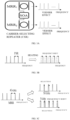
- FIG. 1A illustrates a block diagram of an example communication system in which embodiments of the present disclosure may be implemented.
- the communication system 100 includes at least one access device 110, such as access devices 110-1, 110-2 ?? 110-8, and a processing device 120.
- the access device 110 includes a transmitting device for an Optical Network Unit (ONU) in a Passive Optical Network (PON), a transmitting device for an Access Point (AP) in a wireless backhaul network, and a device for converting a wired network into a wireless network that enable wireless terminal devices such as computers, cell phones, tablets, and the like to connect to a network, such as wireless routers, wireless access points, wireless gateways, and the like.
- ONU Optical Network Unit
- PON Passive Optical Network
- AP Access Point
- the processing device 120 includes, for example, an Optical Line Terminal (OLT) in a passive optical network, a Central Processing Unit (CPU) in a wireless backhaul network, and the like, which includes components, such as a digital subcarrier input interface, a coherent demodulator, a digital signal processor, a DSCM signal output interface, a controller, a memory, and so on, for implementing receiving and demodulation of the DSCM signal.
- the at least one access device 110 transmits modulated valid information of digital subcarrier signals to a processing device 120, which synthesizes the DSCM signals.
- FIG. 1B illustrates a comparison of frequency domain waveforms of a DSCM signal and a single-carrier signal.
- the DSCM signal has more advantages than the single-carrier signal, and the coherent DSCM system is able to flexibly assign different modulation formats, the number of subcarriers and bandwidth, and signal power, etc., to different access devices, and thus is able to solve the problem of flexible slicing of a transmission signal well.
- the digital carrier signal (single-carrier signal) in Fig. 1B has a baud rate of 1*50 GBaud/s, while the DSCM digital subcarrier signal has a baud rate of 8*6.25 GBaud/s.
- the DSCM digital subcarrier signal Compared to single-carrier signals, the DSCM digital subcarrier signal possess advantages of a high bandwidth utilization, strong multi-access capability, high tolerance to linear and nonlinear impairments, and low Enhanced Equalization Phase Noise (EEPN), etc. However, there are also some problems of high complexity and low Peak to Average Power Ratio (PAPR) and so on, at the same time.
- PAPR Peak to Average Power Ratio
- FIG. 1C illustrates a block diagram of an example communication system in which embodiments of the present disclosure may utilize DSCM technology, as illustrated in FIG. 1C , where three different Spoke devices upload a subcarrier signal 10, a subcarrier signal 20, and a subcarrier signal 80 to a Hub device, respectively.
- the problem caused by this is that there is an aliasing between the subcarrier signals from different endpoints.
- Different endpoints transmit subcarrier signals utilizing their own transmitting apparatus Tx, such as Directly Modulated Laser (DML), Electro-absorption Modulated Laser (EML), Edge Emitting Laser (EEL), Vertical Cavity Surface Emitting Laser (VECSEL), etc., and it is common for the wavelength of the laser to drift. Although the degree of wavelength drift of lasers with different qualities will be different, but it will certainly lead to different degrees of signal errors, and data carriers from different endpoints will collide in the frequency domain, i.e., the subcarrier signals are aliased.
- DML Directly Modulated Laser
- EEL Electro-absorption Modulated Laser
- EEL Edge Emitting Laser
- VECSEL Vertical Cavity Surface Emitting Laser
- FIG. 1D illustrates a comparison between an ideal DSCM signal and an uplink DSCM signal in an existing real system.
- the spectrum of the aggregated signals in the Hub device is similar to that on the left figure, and the digital subcarrier signals are contiguous and separated from each other on the spectrum, with each subcarrier signal occupying a portion of the bandwidth.
- the data subcarriers from the eight endpoints will collide in the frequency domain as illustrated in the figure on the right, wherein the subcarrier signal 10 and the subcarrier signal 20 are aliased in the frequency domain.
- the access device 110 in FIG. 1A may be referred to as an access point (AP), an optical network unit (ONU), an endpoint, and the processing device 120 is referred to as a processing unit (CPU), an optical line terminal (OLT), and a relay point in terms of its function.
- AP access point
- ONU optical network unit
- endpoint endpoint
- processing device 120 is referred to as a processing unit (CPU), an optical line terminal (OLT), and a relay point in terms of its function.
- CPU processing unit
- OLT optical line terminal
- the access device 110 is also referred to as a spoke (Spoke) device
- the processing device 120 is also referred to as a hub (Hub) device
- the optical signals are uploaded and downloaded between the access device and the processing device via an optical transmission medium such as an optical fiber
- the optical transmitting apparatus Tx is deployed at the access device 110
- the optical receiving apparatus Rx is deployed at the processing device 120.
- the access device 110 is also referred to as a Tx
- the processing device 120 is also referred to as a Rx, in some embodiments.
- FIG. 1A only schematically illustrates a connection structure between the access device 110 and the processing device 120, wherein data from 8 access devices 110 are aggregated in one processing device 120. It should be noted that the number of access devices 110 as well as processing devices 120 of the embodiments of the present disclosure is not limited to the above example.
- FIG. 2 illustrates a schematic diagram of an interaction flow between an access device and a processing device according to some embodiments of the present disclosure.
- the access device 110 is an access device in the process 200 and the processing device 120 is a processing device in the process 200, for example.
- the access device 110 receives (230) from the processing device 120 at least one carrier signal 205 and a control information 215.
- the at least one carrier signal 205 may be a frequency comb signal that includes one or more optical signals with approximately equal frequency intervals.
- the control information 215 is utilized to indicate the access device 110 how to process and/or modulate the received at least one carrier signal 205, and the control information 215 includes, for example, a position information of a target carrier signal on the frequency spectrum, the number and bandwidth of signal modulation subcarriers, modulation mode of the subcarriers, signal power, and the like.
- the at least one carrier signal 205 and the control information 215 are determined (210) by the processing device 120 for the access device 110, and then sent (220) to the access device 110 through an optical transmission medium such as an optical fiber and so on.
- the access device 110 After receiving the at least one carrier signal 205 and the control information 215 informed by the processing device 120, the access device 110 processes (240) a target carrier signal of the at least one carrier signal 205 based on the control information 215.
- the at least one carrier signal 205 includes, for example, a plurality of frequency comb signals, then the access device 110 first selects a target carrier signal from the plurality of frequency comb signals based on the position of the target carrier signal on the frequency spectrum as indicated in the control information 215, which is a to-be-used carrier signal assigned to the access device 110 by the processing device 120. After obtaining the target carrier signal through frequency selection, the access device 110 processes (240) the target carrier signal.
- the processing (240) of the target carrier signal by the access device 110 may include amplifying the selected target carrier signal to compensate for signal attenuation caused during transmission and assignment from the processing device 120.
- the processing (240) of the target carrier signals by the access device 110 may also include filtering the amplified target carrier signals to reduce noise on the spectrum introduced by the amplification.
- the at least one carrier signal 205 comprises, for example, a single optical carrier signal, whereby the single carrier signal is a to-be-used target carrier signal assigned to the access device 110 by the processing device 120.
- the processing (240) of the target carrier signal by the access device 110 may include amplifying the target carrier signal and filtering the amplified target carrier signal based on the position of the target carrier signal on the spectrum indicated in the control information 215.
- the above-described processing (220) of the target carrier signal may include the above-described general operations of amplifying and filtering the target carrier signal, and may also include other processing processes for the target carrier signal, and any processing process that processes the target carrier signal in at least one carrier signal 205 uniformly informed by the processing device 120 into signals available for the access device 110 (which may be utilized for modulating or transmitting valid information) is applicable to the present embodiment.
- the access device 110 may modulate (250) the target carrier signal based on the control information 215 to generate a modulation signal 225.
- the access device 110 modulates the target carrier signal to generate the modulation signal 225 based on the number and position of the subcarriers, the modulation format of the subcarriers, and the like indicated in the control information 215.
- the modulation signal 225 will be utilized by the access device 110 to transmit valid information to the processing device 120 and to form a digital subcarrier modulation (DSCM) signal at the processing device 120 with other modulation signals 225 from one or more other access devices 110.
- DSCM digital subcarrier modulation
- the access device 110 may transmit (260) the modulation signal 225 to the processing device 120.
- the processing device 120 receives (270) the modulation signal 225 from the access device 110 and combines a plurality of modulation signals 225 uploaded by a plurality of access devices 110 into a DSCM signal and transmits it over the channel, and a corresponding signal receiving side Rx may demodulate by utilized a coherent demodulator to obtain the data sent to that receiving side.
- the subcarrier signals (i.e., the modulation signals 225) uploaded by the eight endpoints (i.e., the access devices 110) illustrated in FIG. 1A may be generated based on the same target carrier signal, or may be generated based on different target carrier signals.
- the processing device 120 may combine a plurality of subcarrier signals generated based on the same target carrier signal, or may combine a plurality of subcarrier signals generated based on different target carrier signals separately.
- subcarrier signals uploaded by the access devices 110-1, 110-2, 110-3, and 110-4 are generated based on the same target carrier signal, and the processing device 120 combines and transmits the subcarrier signals from the access devices 110-1, 110-2, 110-3, and 110-4 into a complete DSCM signal; subcarrier signals uploaded by the access devices 110-5, 110-6, 110-7 and 110-8 are generated based on the same target carrier signal, and the processing device 120 then combines and transmits the subcarrier signals from the access devices 110-5, 110-6, 110-7 and 110-8 into a complete DSCM signal.
- Embodiments of the present disclosure propose a scheme for uniformly informing carrier signals by a processing device, thereby reducing aliasing of modulated signals from different access devices in the frequency domain, improving quality of the DSCM signal, and facilitating realization of elastic high-speed optical networks.
- processing of the target carrier signal of the at least one carrier signal 205 in the interaction process 200 is accomplished by a Carrier Selecting Repeater (CSR) deployed at the access device 110.
- CSR Carrier Selecting Repeater
- the at least one carrier signal 205 comprises, for example, a frequency comb signal.
- FIG. 3A illustrates a schematic diagram of a CSR in these embodiments.
- the CSR includes a first Micro Ring Resonator (MRR) MRR1, the first micro-ring resonator MRR1 receives the at least one carrier signal 205 informed by the processing device 120, and adjusts a resonant wavelength of the MRR1 by heating the waveguide of the MRR1 to shift a passband of a plurality of passbands of the MRR1 to move to a frequency position of the target carrier signal, thereby selecting the target carrier signal from the at least one carrier signal 205.
- MRR Micro Ring Resonator
- the operation principle of the first micro-ring resonator is exemplarily described below.
- the resonant wavelength of MRR1 is shifted by heating a microheater deposited on the first micro-ring resonator MRR1 to select the desired carrier.
- a vernier effect is applied to the alignment of the resonant wavelength of MRR1 with the selected carriers to reduce the frequency shift of the transmission spectrum of MRR1, thereby reducing the delay.
- the carrier signal needed to be selected of the plurality of informed frequency comb signals are aligned, i.e., the target carrier signal is filtered out from at least one carrier signal.
- Figure 3B illustrates a heating frequency shift process of the micro-ring resonator.
- an optical transmission spectrum of MRR1 is illustrated in the left part of Fig.3B . Due to the resonance effect, it exhibits multiple bandpass filter effects, e.g., the Free Spectral Range (FSR) of MRR1 is compatible with the frequency spacing of the informed frequency comb.
- FSR Free Spectral Range
- Micro heaters deposited on the arms of MRR1 can be heated by electric current to shift the transmission spectrum of MRR1, as illustrated in the right part of FIG. 3B .
- FIG. 3C illustrates a process of MRR selecting signals utilizing the Vernier effect. As illustrated in FIG. 3C , for a normal bandpass filter with only one passband, if one wants to pick out other carrier signal rather than the one utilized before, frequency shifting equal to the frequency spacing between two successive carrier signals is required (it may set the frequency spacing between adjacent carrier signals to be 45 GHz).
- the carrier selecting repeater CSR provided in some embodiments of the present disclosure, it is only necessary to shift a smaller difference in frequency spacing (the difference between adjacent passbands of the micro-ring resonators) of 5 GHz, thereby reducing the delay and energy of the heating process in the micro-ring resonator MRR.
- the CSR further comprises a Semiconductor Optical Amplifier SOA and a second micro-ring resonator MRR2, wherein an input end of the Semiconductor Optical Amplifier SOA is coupled to an output end of the MRR1, and an output end of the SOA is coupled to an input end of the MRR2, wherein:
- the SOA Based on the signal power information indicated in the control information 215, the SOA amplifies the target carrier signal.
- a case of the CSR including a single semiconductor optical amplifier SOA is only schematically illustrated in FIG. 3A , and it is readily appreciated by a person skilled in the art that a plurality of semiconductor optical amplifiers in cascade may also be utilized to amplify the target carrier signal in the present instance.
- MRR2 receives the amplified target carrier signal and filters the amplified target carrier signal by adjusting the resonant wavelength of MRR2 to filter out the amplified spontaneous emission (ASE) noise introduced by the SOA.
- ASE amplified spontaneous emission
- MRR1, MRR2, and the SOA connected in series between them form a carrier selecting repeater CSR.
- a desired carrier can be selected by shifting the resonant wavelength of MRR1. It may reduce the frequency shift of the transmission spectrum of the MRR1 by utilizing the Vernier effect to make alignment.
- the SOA connected in series between the MRRs amplifies the selected target carrier signals to compensate for the optical power loss from fiber optic transmission and power splitter among the plurality of access devices.
- a signal power of the target carrier signal can be adjusted by adjusting the input electric current to the SOA, so that the power of the subcarrier signals uploaded by the respective access devices meets the requirement of the power balance of the respective subcarrier in a coherent DSCM signal.
- the optical loss of the carrier signals in the process of transmission and power splitter is very large and can be compensated by utilizing a cascaded SOA.
- MRR2 is utilized to filter out the ASE noise caused by the SOA.
- MRR2 is a replication device of MRR1 with the same fabric area and FSR.
- the identical or similar (error within the preset range) temperature control is applied in both MRRs to guarantee the same frequency shift of the resonant wavelength.
- the MRR1, MRR2, and SOA may be fabricated utilizing Photonic Integrated Circuit (PIC) technology, to make the CSR module compact, energy efficient, and cost effective. This is very benefit for the CSR application in optical access domain, which requires small footprint, high power efficiency and low cost.
- PIC Photonic Integrated Circuit
- the processing of the optical signal by the CSR is illustrated in FIG. 3D , where the at least one carrier signal 215 includes a plurality of frequency comb signals having the same frequency spacing, a target carrier signal therein therein is selected by tuning of MRR1, and the target carrier signal is amplified by the SOA, and the amplification process generates the ground noise of spontaneous radiation, then the amplified target carrier signal is filtered by MRR2, and the signal frequency is aligned by the tuning of MRR2, and the noise of the other frequencies of the frequency spectrum is filtered out.
- the CSR comprises a semiconductor optical amplifier SOA and a second micro-ring resonator MRR2.
- a target carrier signal is amplified through the SOA by coupling the SOA to the MRR2 based on signal power information indicated in the control information 215.
- the MRR2 receives the amplified target carrier signal and filters the amplified target carrier signal by adjusting a resonant wavelength of the MRR2 to filter out amplified spontaneous emission (ASE) noise introduced by the SOA based on position information of the target carrier signal on the frequency spectrum indicated in the control information 215.
- ASE amplified spontaneous emission
- the access device 110 further comprises at least one modulator, the at least one modulator coupled to an output end of the MRR2, modulating the filtered target carrier signal by a modulator to generate a modulation signal. Based on information such as the number and bandwidth of subcarriers, signal modulation format, etc., indicated in the control information 215, the at least one modulator modulates the target carrier signal to generate a modulation signal 225.
- the at least one modulator is integrated in the same module with the MRR1, the MRR2, and the SOA by photonic integrated circuit technology.
- High-speed modulators of small size compatible with silicon photonics technology developed utilizing hybrid integration routes, such as hybrid silicon-organic modulators and plasma modulators are suitable for embodiments of the present disclosure.
- the CSR module can be integrated with such modulators based on advanced PIC technology to build a DSCM transmitter-side Tx integrated system.
- FIG. 4 illustrates a block diagram of an example communication system and its internal components in which embodiments of the present disclosure may be implemented.
- a Spoke device receives a frequency comb signal informed by a Hub device and generated by a frequency comb generator.
- a CSR module and a transmitter Tx of a modulator are integrated at the Spoke device side.
- the Spoke device may process and modulate the frequency comb signal based on control information 215, and generate a modulation signal 225, the Spoke device transmits the modulation signal to a Hub device, and a coherent receiver Rx at the Hub device side receives the modulation signal uploaded by the respective Spoke device, and combines the modulation signals to form a DSCM signal.
- FIG. 5 illustrates a schematic diagram of a CSR module and its internal components of an embodiment of the present disclosure.
- micro heaters H1 and H2 are set on MRR1 and MRR2 respectively, and light detectors PD1 and PD2 are coupled at the output ports of MRR1 and MRR2.
- a portion of the output optical signals of MRR1 and MRR2 are received by PD1 and PD2 respectively, and the input electric currents of the micro heaters H1 and H2 on MRR1 and MRR2 are adjusted based on the signal strength of the portion of the output signals to adjust the resonant wavelengths of MRR1 and MRR2.
- Two photodetectors PD1, PD2 are coupled to the output ports of the first micro-ring resonator and the second micro-ring resonator.
- PD1, PD2 are utilized to check the alignment of the transmit spectrum and receive frequency comb of MRR1, MRR2.
- a very small part of power of the optical signal output from MRR1 and MRR2 is injected into PD1 and PD2.
- Ic is an input electric current to the SOA for adjusting the signal power (amplification) during signal amplification, so that the modulation signals 225 uploaded by the respective access devices 110 meet the requirement for a power balance between the respective modulation signals 225 when synthesizing the DSCM signal at the processing device 120.
- the processing device 120 informs the at least one carrier signal 205 over a fiber optic channel, and due to the different lengths of the transmission fibers, it may need to control the output power of the optical signals from the different access devices 110 in order to maintain a power balance within the DSCM signal. This may be accomplished by adjusting the input electric current of the SOA.
- the power of the target carrier signal is determined based on the transmission distance between the access device 110 and the processing device 120.
- the processing device 120 performs ranging at an early stage of establishing a connection and records the signal transmission distance with the access device 110, the processing device 120 determines the power of the target carrier signal and writes into the control information 215 based on the transmission distance.
- the access device 110 performs power amplification of the target carrier signal 115 based on the control information 215.
- the modulation signal obtained by modulating the target carrier signal by a modulator is located on one or both sides of the target carrier signal on the spectrum (i.e., the target carrier signal is modulated), such that the target carrier signal is at the edge of a subcarrier bandwidth of the DSCM signal.
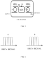
- FIG. 6 illustrates a schematic diagram of a relationship between a carrier signal and a subcarrier signal on the spectrum of an embodiment of the present disclosure.
- the subcarrier signals are placed at the edge of, e.g., the target carrier signal (on the left of FIG. 6 ), instead of placing the subcarrier signals in the center of the target carrier signal (on the right of FIG. 6 ), to mitigate the impact of residual amplifier noise, e.g., SOA noise, and reflective noise generated by the downlink frequency comb.
- residual amplifier noise e.g., SOA noise
- reflective noise generated by the downlink frequency comb.
- the access device 110 prior to receiving the at least one carrier signal 205 and the control information 215, transmits traffic demand information of the access device 110 to the processing device 120, wherein the at least one carrier signal 205 and the control information 215 are determined based on the traffic demand information.
- FIG. 7 illustrates a schematic diagram of an interaction process between the access device 110 and the processing device 120 of an embodiment of the present disclosure.
- the access device 110 establishes a connection with the processing device 120.
- the access device 110 establishes a control channel of a preset frequency band with the processing device 120.
- the access device 110 and the processing device 120 communicate utilizing this control channel, and the access device 110 transmits (720) information, such as traffic demand, to the processing device 120, which utilizes the control channel to query (730) the traffic request, synchronize information, make measurements of the transmission distance, and the like. That is, before receiving the at least one carrier signal 205 and the control information 215, the access device 110 utilizes the control channel between the access device 110 and the processing device 120 to perform an activation (710) process of the access device 110.
- the processing device 120 transmits the at least one carrier signal 205 and the control information 215 to the access device 110, the at least one carrier signal 205 and the control information 215 being generated based on the traffic demand information.
- the processing device 120 allocates channels according to the traffic demand information of respective access devices 110, determines (740) a target carrier signal position, the number and bandwidth of subcarrier signals, a modulation mode, a signal power, and the like corresponding to respective access devices 110. That is, the processing device 120 generates the at least one carrier signal 205 and the control information 215 based on the traffic demand information.
- the processing device 120 may employ a mode-locked laser to generate the required at least one carrier signal 205, for example, to generate a single optical carrier signal or a frequency comb signal, and inform (750) the one or more frequency comb signals and the associated allocation information to the access device 110 to which it is connected.
- a mode-locked laser to generate the required at least one carrier signal 205, for example, to generate a single optical carrier signal or a frequency comb signal, and inform (750) the one or more frequency comb signals and the associated allocation information to the access device 110 to which it is connected.
- the access device 110 based on the control information 215, adjusts (760) the CSR, filters out one or more carrier signals in this frequency comb, selects a frequency comb signal corresponding to the access device 110, and modulates (770) the corresponding carrier signal according to information such as the allocated subcarrier bandwidth, modulation format, and so on.
- the processing device 120 informs the at least one carrier signal 205 and the control information 215 to the access device 110, wherein the control information 215 is informed through a control channel of a preset frequency band, in which the control channel should be isolated from the frequency band of the allocated carrier signal on the spectrum.
- the control channel may be at least one digital subcarrier of a plurality of digital subcarriers in the communication spectrum between the access device 110 and the processing device 120, or, the control channel may be at least one wavelength in the communication spectrum between the access device 110 and the processing device 120.
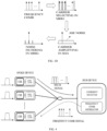
- FIG. 8A illustrates a block diagram of an example communication system in which embodiments of the present disclosure may upload and download signals, as well as perform carrier allocation and modulation.
- an access point AP may be comprised of different devices, such as a radio unit RU, or a RU + a distributed unit DU, or a RU + a DU + a centralized unit CU.
- the corresponding data transmission between the AP and the centralized processing unit CPU is defined as forward, intermediate, and backhaul, collectively referred to as xhaul.
- the CPU located in the centralized office CO receives and processes all data from different APs.
- the xhaul system in this embodiment consists of four APs (AP1, AP2, AP3, and AP4) and one CPU, connected via optical fibers with a tree topology.
- a frequency comb generator (Freq. Comb Gen.) in the CPU generates two carriers with wavelengths ⁇ 1 and ⁇ 2, with 50 GHz of frequency spacing.
- Freq. Comb Gen. in the CPU generates two carriers with wavelengths ⁇ 1 and ⁇ 2, with 50 GHz of frequency spacing.
- There are various methods of generating the frequency comb one of which is to utilize a mode-locked laser.
- the downstream carrier After transmission through the backbone fiber, the downstream carrier is coupled into four distributed fibers of different lengths.
- the allocated carriers decided by the CPU are selected and modulated by utilizing a carrier selecting repeater CSR and a modulation module as described above, according to the traffic demand and channel state information of the AP.
- the structure of the CSR deployed in the AP is as described above, and the free spectral range FSR of the micro-ring resonator MRR in the CSR is 45 GHz, which is compatible with the frequency spacing of the downlink frequency comb.
- the free spectral range FSR of the micro-ring resonator MRR in the CSR is 45 GHz, which is compatible with the frequency spacing of the downlink frequency comb.
- a frequency shift of 50 GHz should be performed.
- different carriers for CSR3 and CSR4 than for CSR1 and CSR2 can be selected by shifting the frequency by only 5 GHz, thus reducing the delay and energy of the heating process in the MRR. It is beneficial in reducing the frequency shift by minimizing the difference between the FSR value and the frequency spacing of the MRR when selecting carriers in the CSR module.
- AP1 is closer to the CPU (5km) while AP2 is further away from the CPU (10km), AP1 and AP2 receive carrier signals at different transmission distances, but AP1 and AP2 are allocated to the same carrier signal, and their uploaded sub-carrier signals will be combined into the same DSCM signal for transmission, therefore, it may need to process the carrier signals at AP1 and/or AP2, and AP2 should amplify the carrier signals more in order to be balanced with the carrier signal of AP1.
- FIG. 8B illustrates a schematic diagram of a process of selecting a target carrier signal and modulating a sub-carrier signal for the access device 110 of an embodiment of the present disclosure.
- the output power of AP2 and AP4 should be approximately 1 dB more than the output power of AP1 and AP3. This can be achieved by adjusting the input electric current of the SOA.
- the AP modulates the filtered target carrier signals to generate the subcarrier signals SC, and the bandwidth, the number, position on the spectrum, etc., of the subcarrier signals SC are determined by the CPU and included in the control information to be informed, and the AP modulates the allocated target carrier signals based on the control information to generate the subcarrier signals SC as illustrated in FIG. 8B .
- AP1 and AP2 each occupy two subcarrier signals SC.
- one and three subcarrier signals SC are allocated respectively.
- the modulation formats of AP1 and AP3 can be upgraded to a higher level of quadrature amplitude modulation QAM, because of their shorter fiber optic transmission lengths and improved spectral efficiency. That is, a combination of transformations by utilizing other modulation methods, or using other number and bandwidth of the subcarrier signals, position of the subcarrier signals on the spectrum, etc., can be utilized to implement the present disclosure.
- the output signals from the four APs are sent back to the CPU, and in the CPU, the signals from AP1 and AP2 are combined into a complete DSCM signal, and the signals from AP3 and AP4 are combined into another complete DSCM signal.
- a coherent receiver (Coh. Rx) 1 and a coherent receiver 2 are utilized to receive and process individual DSCM signals of different wavelengths. In some other embodiments, one or more coherent receivers may be utilized to receive and process DSCM signals from the AP.
- Embodiments of the present disclosure present a digital subcarrier multiplexing scheme based on carrier signals informed from a Hub, which avoids collisions in frequency domain of signals from different APs since the transmitter module in the AP just selects and amplifies carriers in the frequency comb from the same Hub.
- the effective data transmission performance utilizing DSCM is improved and can be utilized in multi-wavelength system to satisfy the capacity requirement of beyond Tb/s for next generation optical metro/access networks.
- the access device 110 utilizes the subcarrier signals to transmit valid information to the processing device 120 until the communication demand at the access device 110 changes, at which time the access device 110 retransmits the traffic demand information to the processing device 120.
- the access device 110 selects a target carrier signal according to the control information and modulates a modulation signal, utilizes the modulation signal to transmit valid information to the processing device 120, and starts a normal communication between the access device 110 and the processing device 120 until the traffic demand at the access device 110 changes.
- the access device 110 retransmits the traffic demand information to the processing device 120, and the processing device 120 implements operations such as ranging, synchronization, and querying the traffic demand and so on, and allocates carrier signals and control information according to the channel conditions and the traffic demand information, and informs them to the access device 110.
- the processing device 120 and the access device 110 may communicate through the control channel, and the frequency band of the control channel may be different from the frequency band of the carrier signal. More specifically, the access device 110 may transmit communication demand information via the control channel, the access device 110 may receive the control information informed by the processing device 120 via the control channel, and/or the processing device 120 may measure a signal transmission distance via the control channel. In some examples, the access device 110 may connect to the processing device 120 utilizing the control channel. After the connection established, the processing device 120 implements general operations such as ranging, synchronization, and querying the traffic demand and so on. Communication between the access device 110 and the processing device 120 may be difficult during the activation process of the control channel, and therefore, in some embodiments, specific subcarrier frequency bands or wavelengths are reserved as the control channel.
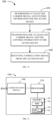
- FIG. 9 illustrates a schematic diagram of a process performed by access device 110 according to some embodiments of the present disclosure.
- the process 900 of FIG. 9 will be described with reference to FIG. 1A .
- the access device 110 receives at least one carrier signal and control information from the processing device 120.
- the access device 110 processes a target carrier signal of the at least one carrier signal.
- the access device 110 modulates the target carrier signal to generate a modulation signal, wherein the modulation signal will be combined with other modulation signals from one or more other access devices at the processing device 120 to form a digital subcarrier modulation (DSCM) signal.
- DSCM digital subcarrier modulation
- the access device 110 transmits the modulation signal to the processing device 120.
- the access device 110 processes the target carrier signals by: amplifying the target carrier signal utilizing at least one semiconductor optical amplifier (SOA) based on a signal power information indicated in the control information; and filtering out amplified spontaneous emission (ASE) noise introduced by the at least one SOA utilizing a micro-ring resonator (MRR).
- SOA semiconductor optical amplifier
- MRR micro-ring resonator
- the access device 110 further selects the target carrier signal from the plurality of carrier signals utilizing the first MRR based on a frequency position of the target carrier signal indicated in the control information.
- the access device 110 utilizes the first MRR by: heating a waveguide of the first MRR to shift a passband of a plurality of passbands of the first MRR to the frequency position of the target carrier signal.
- the access device 110 utilizes the at least one SOA by: adjusting an input electric current of the at least one SOA based on a signal power information indicated in the control information.
- the second MRR is a replication device of the first MRR, and the second MRR is applied to temperature controlling similar to that of the first MRR to cause a passband of a plurality of passbands of the second MRR to shift to a frequency position of the target carrier signal.
- micro heaters are set on the first MRR and the second MRR; or, a photo detector (PD) is coupled at output ports of the first MRR and the second MRR.
- PD photo detector
- the first MRR, the SOA, and the second MRR are integrated in a single module based on photonic integrated circuit (PIC) technology.
- PIC photonic integrated circuit
- At least one modulator is integrated in the single module based on PIC technology.
- the target carrier signal is modulated such that the target carrier signal is at an edge of a subcarrier bandwidth of the DSCM signal.
- the access device 110 transmits traffic demand information of the access device 110 to the processing device 120 prior to receiving the at least one carrier signal and the control information, wherein the at least one carrier signal and the control information are determined based on the traffic demand information.
- the access device 110 utilizes a control channel between the access device 110 and the processing device 120 to perform an activation process of the access device 110 prior to receiving the at least one carrier signal and the control information.
- At least one of the following is configured as the control channel: at least one digital subcarrier of a plurality of digital subcarriers in a communication spectrum between the access device 110 and the processing device 120; or at least one wavelength in the communication spectrum.
- the at least one carrier signal comprises a frequency comb signal
- the control information comprises one or more of: a position of the target carrier on the spectrum, the number of subcarriers for the access device 110, bandwidth of the subcarriers, a signal modulation format for the access device 110, or a power of the subcarrier signal for the access device 110.
- a free spectral range (FSR) of the first MRR is determined based on a frequency spacing of the frequency comb signal.
- the number of subcarriers, the bandwidth of the subcarriers, and the modulation format are determined based on spectral efficiency and system performance.
- FIG. 10 illustrates a schematic diagram of a process performed by the processing device 120 according to some embodiments of the present disclosure. For ease of description, the flow 1000 of FIG. 10 will be described with reference to FIG. 1A .
- the processing device 120 determines at least one carrier signal and control information for the access device 110.
- the processing device 120 transmits the at least one carrier signal and the control information to the access device 110.
- a modulation signal is received from the access device 110, wherein the modulation signal is generated by modulating a target carrier signal of the at least one carrier signal based on the control information, and wherein the modulation signal is combined with other modulation signals of one or more other access devices 110 at the processing device 120 to form a digital subcarrier modulation (DSCM) signal.
- DSCM digital subcarrier modulation
- the processing device 120 determines the at least one carrier signal and the control information by: receiving traffic demand information for the access device 110 from the access device 110; and determining the at least one carrier signal and the control information based on the received traffic demand information and channel state information associated with the access device 110.
- the processing device 120 performs an activation process of the access device 110 utilizing a control channel between the processing device 120 and the access device 110 prior to determining the at least one carrier signal and the control information.
- At least one of the following is configured as the control channel: at least one digital subcarrier of a plurality of digital subcarriers in a communication spectrum between the processing device 120 and the access device 110; or at least one wavelength in the communication spectrum.
- the processing device 120 receives a plurality of DSCM signals from the plurality of access devices 110 utilizing one or more coherent receivers; and processes the plurality of DSCM signals utilizing the one or more coherent receivers.
- the target carrier signal is at an edge of a subcarrier bandwidth of the DSCM signal.
- the at least one carrier signal comprises a frequency comb signal
- the control information comprises one or more of: a position of the target carrier on the spectrum, the number of subcarriers for the access device 110, bandwidth of the subcarriers, a signal modulation format for the access device 110, or a power of the subcarrier signals for the access device 110.
- the number of subcarriers, the bandwidth of the subcarriers, and the modulation format are determined based on spectral efficiency and system performance.
- an apparatus capable of performing the method 900 may include means for performing various steps of the method 900.
- the means may be implemented in any suitable form.
- the means may be implemented in a circuit or software module.
- the apparatus includes: means for receiving, at an access device, at least one carrier signal and control information from a processing device; means for processing a target carrier signal of the at least one carrier signal based on the control information; means for modulating the target carrier signal based on the control information to generate a modulation signal, wherein the modulation signal will be combined with other modulation signals of one or more other access devices at the processing device to form a digital subcarrier modulation (DSCM) signal; and means for transmitting the modulation signal to the processing device.
- DSCM digital subcarrier modulation
- the means for processing the target carrier signal include: means for amplifying the target carrier signal utilizing at least one semiconductor optical amplifier (SOA) based on signal power information indicated in the control information; and means for filtering amplified spontaneous emission (ASE) noise introduced by the at least one SOA utilizing a micro-ring resonator (MRR).
- SOA semiconductor optical amplifier
- MRR micro-ring resonator
- the apparatus further comprises: means for selecting the target carrier signal from a plurality of carrier signals utilizing the first MRR based on a frequency position of the target carrier signal indicated in the control information.
- the means for utilizing the first MRR comprises: means for heating a waveguide of the first MRR to shift a passband of a plurality of passbands of the first MRR to the frequency position of the target carrier signal.
- the means for utilizing the at least one SOA includes: means for adjusting an input electric current of the at least one SOA based on signal power information indicated in the control information.
- the second MRR is a replication device of the first MRR, and the second MRR is applied to temperature controlling similar to that of the first MRR to cause a passband of a plurality of passbands of the second MRR to be shifted to the frequency position of the target carrier signal.
- micro heaters are set on the first MRR and the second MRR; or a photo detector (PD) is coupled at the output ports of the first MRR and the second MRR.
- PD photo detector
- the first MRR, the SOA, and the second MRR are integrated in a single module based on photonic integrated circuit (PIC) technology.
- PIC photonic integrated circuit
- the at least one modulator is integrated in the single module based on PIC technology.
- the target carrier signal is modulated such that the target carrier signal is at an edge of a subcarrier bandwidth of the DSCM signal.
- the apparatus further comprises: means for transmitting traffic demand information of the access device to the processing device prior to receiving the at least one carrier signal and the control information, wherein the at least one carrier signal and the control information are determined based on the traffic demand information.
- the apparatus further comprises: means for performing an activation process of the access device utilizing a control channel between the access device and the processing device prior to receiving the at least one carrier signal and the control information.
- At least one of the following is configured as the control channel: at least one digital subcarrier of a plurality of digital subcarriers in a communication spectrum between the access device and the processing device; or at least one wavelength in the communication spectrum.
- the at least one carrier signal comprises a frequency comb signal
- the control information comprises one or more of: a position of the target carrier on the spectrum, the number of subcarriers for the access device, bandwidth of the subcarriers, a signal modulation format for the access device, or a power of the subcarrier signal for the access device.
- a free spectral range (FSR) of the first MRR is determined based on a frequency spacing of the frequency comb signal.
- the number of subcarriers, the bandwidth of the subcarriers, and the modulation format are determined based on spectral efficiency and system performance.
- an apparatus capable of performing the method 1000 may include means for performing various steps of the method 1000.
- the means may be implemented in any suitable form.
- the means may be implemented in a circuit or software module.
- the apparatus includes: means for determining, at a processing device, at least one carrier signal and control information for an access device; means for transmitting the at least one carrier signal and the control information to the access device; and means for receiving a modulation signal from the access device, wherein the modulation signal is generated by modulating a target carrier signal of the at least one carrier signal based on the control information, and wherein the modulation signal is combined with other modulation signals of one or more other access devices at the processing device to form a digital subcarrier modulation (DSCM) signal.
- DSCM digital subcarrier modulation
- the means for determining the at least one carrier signal and the control information include: means for receiving traffic demand information of the access device from the access device; and means for determining the at least one carrier signal and the control information based on the received traffic demand information and channel state information associated with the access device.
- the apparatus further comprises: means for performing an activation process of the access device utilizing a control channel between the processing device and the access device prior to determining the at least one carrier signal and the control information.
- At least one of the following is configured as the control channel: at least one digital subcarrier of a plurality of digital subcarriers in a communication spectrum between the processing device and the access device; or at least one wavelength in the communication spectrum.
- the apparatus further comprises: means for receiving a plurality of DSCM signals from a plurality of access devices utilizing one or more coherent receivers; and means for processing the plurality of DSCM signals utilizing the one or more coherent receivers.
- the target carrier signal is at an edge of a subcarrier bandwidth of the DSCM signal.
- the at least one carrier signal comprises a frequency comb signal
- the control information comprises one or more of: a position of the target carrier on the spectrum, the number of subcarriers for the access device, bandwidth of the subcarriers, a signal modulation format for the access device, or a power of the subcarrier signals for the access device.
- the number of subcarriers, the bandwidth of the subcarriers, and the modulation format are determined based on spectral efficiency and system performance.
- FIG. 11 is a simplified block diagram of an electronic device 1100 suitable for implementing embodiments of the present disclosure.
- the device 1100 may be provided to implement an access device or a processing device, such as the access device 110 or the processing device 120 as illustrated in FIG. 1A .
- the device 1100 includes one or more processors 1110, one or more memories 1120 coupled to the processors 1110, and one or more communication modules 1140 coupled to the processors 1110.
- the communication module 1140 is utilized for bi-directional communication, for example, the communication module 1140 may include a transmitter, receiver, or transceiver for embodiments of the present disclosure.
- the communication interface may represent any interface necessary to communicate with other network elements.
- the processor 1110 may be of any type suitable for a local technology network and may include, but is not limited to, one or more of a general purpose computer, a specialized computer, a microcontroller, a digital signal controller (DSP), and a controller-based multi-core controller architecture.
- the device 1100 may have a plurality of processors, such as dedicated integrated circuit chips, that are temporally subordinate to a clock synchronized with a main processor.
- the memory 1120 may include one or more non-volatile memories and one or more volatile memories.
- non-volatile memory include, but are not limited to, read-only memory (ROM) 1124, erasable programmable read-only memory (EPROM), flash memory, hard disks, compact discs (CDs), digital video disks (DVDs), and other magnetic and/or optical storage.
- volatile memory include, but are not limited to, random access memory (RAM) 1122 and other volatile memory that does not persist for a duration of power off.
- the computer program 1130 includes computer executable instructions executed by the associated processor 1110.
- the program 1130 may be stored in ROM 1120.
- the processor 1110 may perform any suitable actions and processing by loading the program 1130 into RAM 1122.
- Embodiments of the present disclosure can be implemented with the aid of the program 1130, allowing the device 1100 to perform any of the processes of the present disclosure as discussed with reference to FIG. 2 .
- Embodiments of the present disclosure may also be implemented by hardware or by a combination of software and hardware.
- the program 1130 may be tangibly contained in a computer-readable medium, which may be included in the device 1100 (e.g., in the memory 1120) or other storage device accessible by the device 1100.
- the program 1130 may be loaded from the computer-readable medium into RAM 1122 for execution.
- the computer-readable medium may include any type of tangible, non-volatile memory, such as ROM, EPROM, flash memory, hard disk, CD, DVD, and the like.
- FIG. 12 illustrates an example of a computer readable medium 1200 in the form of a CD or DVD.
- the computer-readable medium has a program 1130 stored on it.
- various embodiments of the present disclosure may be implemented in hardware or specialized circuitry, software, logic, or any combination thereof. Some aspects may be implemented in hardware, while other aspects may be implemented in firmware or software, which may be executed by a controller, microprocessor, or other computing device. While aspects of embodiments of the present disclosure are illustrated and described as block diagrams, flowcharts, or utilizing some other graphical representation, it should be understood that the block, apparatus, system, technique, or method described herein may be implemented as, e.g., non-limiting examples, hardware, software, firmware, specialized circuitry or logic, general-purpose hardware, or controllers or other computing devices, or some combination thereof.
- the present disclosure also provides at least one computer program product tangibly stored on a non-transitory computer readable storage medium.
- the computer program product includes computer-executable instructions, such as instructions included in a program module, which are executed in a device on a real or virtual processor of a target to perform the methods 900, 1000 as referenced above in FIGS. 9 to 10 .
- program modules include routines, programs, libraries, objects, classes, components, data structures, and the like that perform specific tasks or implement specific abstract data types.
- the functionality of program modules may be combined or partitioned between program modules as desired.
- Machine-executable instructions for the program modules may be executed locally or within a distributed device. In a distributed device, the program modules may be located in both local and remote storage media.
- Computer program code for implementing the methods of the present disclosure may be written in one or more programming languages. These computer program codes may be provided to a general-purpose computer, a specialized computer, or a processor of other programmable data processing device, such that the program code, when executed by the computer or other programmable data processing device, causes the functions/operations specified in a flowchart and/or block diagram to be implemented.
- the program code may be executed entirely on a computer, partially on a computer, as a stand-alone software package, partially on a computer and partially on a remote computer, or entirely on a remote computer or server.
- the computer program code or associated data may be carried by any suitable carrier to enable a device, an apparatus, or a processor to perform the various processing and operations described above.
- suitable carriers include signals, computer readable media, and the like.
- signals may include electricity, light, radio, sound, or other forms of propagated signals, such as carrier waves, infrared signals, and the like.
- a computer-readable medium may be any tangible medium that contains or stores a program for or about an instruction-executing system, apparatus, or device.
- the computer-readable medium may be a computer-readable signal medium or a computer-readable storage medium.
- the computer-readable medium may include, but is not limited to, an electronic, magnetic, optical, electromagnetic, infrared, or semiconductor system, apparatus, or device, or any suitable combination thereof. More detailed examples of computer-readable storage media include an electrical connection with one or more wires, a portable computer disk, a hard disk, a random-access memory (RAM), a read-only memory (ROM), an erasable programmable read-only memory (EPROM or flash memory), an optical storage device, a magnetic storage device, or any suitable combination thereof.
- the terms "non-transitory” or “non-transient” define the medium itself (i.e., tangible, not signal) and not the definition for data storage persistence (e.g., RAM and ROM).
Landscapes
- Engineering & Computer Science (AREA)
- Computer Networks & Wireless Communication (AREA)
- Signal Processing (AREA)
- Physics & Mathematics (AREA)
- Electromagnetism (AREA)
- Optics & Photonics (AREA)
- Optical Communication System (AREA)
Abstract
Embodiments of the present disclosure relate to an access device, a processing device, an associated method, an apparatus, and a medium. In one aspect, the access device receives at least one carrier signal and control information from the processing device. The access device processes a target carrier signal of the at least one carrier signal based on the control information. The access device modulates the target carrier signal based on the control information to generate a modulation signal, wherein the modulation signal will be combined with other modulation signals of one or more other access devices at the processing device to form a digital subcarrier modulation (DSCM) signal. The access device then transmits the modulation signal to the processing device. Embodiments of the present disclosure uniformly inform the carrier signals by the processing device, thereby reducing aliasing of modulated signals from different access devices in the frequency domain, improving the quality of the DSCM signals, and facilitating the realization of flexible high-speed optical networks.
Description
- Embodiments of the present disclosure generally related to the field of communications technology and more specifically, to access devices, processing devices, related methods, related apparatus, and computer-readable media.
- With the continuously explosive increase of data traffic in the Internet, the required transmission capacity of the core, metro and access networks is growing rapidly over the time. Higher baud rate, higher-order modulation format, advanced digital signal processing (DSP) and forward error correction (FEC), and other advanced digital communication techniques are adopted recently in industry to further push the throughput to the limit.
- To cope with the current rapid traffic evolution, efficiently exploiting the already-deployed fiber infrastructure is an important way, which can postpone the costly deployment of new fibers. In this strategy, flexible slicing capability of transmitted signal is a paramount factor to realize more efficient management of network resources. However, traditional coherent scheme based on single carrier modulation lack this capability.
- In general, example embodiments of the present disclosure relate to a technical solution for uniformly placing carrier signals by a processing device to a plurality of access devices, and for processing and/or modulating a target carrier signal by the access device, for optimizing performance of a point-to-multipoint (PtMP) coherent digital subcarrier modulation (DSCM) system.
- In a first aspect of the disclosure, there is provided an access device is provided. The access device comprises: at least one processor and at least one memory. The at least one memory stores instructions, and the instructions, when executed by the at least one processor, cause the access device at least to: receive at least one carrier signal and control information from the processing device; process a target carrier signal of the at least one carrier signal based on the control information; modulate the target carrier signal based on the control information to generate a modulation signal, wherein the modulation signal will be combined with other modulation signal of one or more other access devices at the processing device to form a digital subcarrier modulation (DSCM) signal; and transmit the modulation signal to the processing device.
- In a second aspect of the disclosure, there is provided a processing device. The processing device comprises: at least one processor and at least one memory. The at least one memory stores instructions, the instructions, when executed by the at least one processor, causing the processing device to at least: determine at least one carrier signal and control information for an access device; transmit the at least one carrier signal and the control information to the access device; and receive a modulation signal from the access device, wherein the modulation signal is generated by modulating a target carrier signal of the at least one carrier signal based on the control information, and wherein the modulation signal is combined with other modulation signals of one or more other access devices at the processing device to form a digital subcarrier modulation (DSCM) signal.
- In a third aspect of the disclosure, there is provided a method. The method comprises: receiving, at an access device, at least one carrier signal and control information from a processing device; processing a target carrier signal of the at least one carrier signal based on the control information; modulating the target carrier signal based on the control information to generate a modulation signal, wherein the modulation signal will be combined with other modulation signals of one or more other access devices at the processing device to form a digital subcarrier modulation (DSCM) signal; and transmitting the modulation signal to the processing device.
- In a fourth aspect of the disclosure, there is provided a method. The method comprises: determining, at a processing device, at least one carrier signal and control information for an access device; transmitting the at least one carrier signal and the control information to the access device; and receiving a modulation signal from the access device, wherein the modulation signal is generated by modulating a target carrier signal of the at least one carrier signal based on the control information, and wherein the modulation signal is combined with other modulation signals of one or more other access devices at the processing device to form a digital subcarrier modulation (DSCM) signal.
- In a fifth aspect of the disclosure, there is provided an apparatus. The apparatus comprises: means for receiving, at an access device, at least one carrier signal and control information from a processing device; means for processing a target carrier signal of the at least one carrier signal based on the control information; means for modulating the target carrier signal based on the control information to generate a modulation signal, wherein the modulation signal will be combined with other modulation signals of one or more other access devices at the processing device to form a digital subcarrier modulation (DSCM) signal; and means for transmitting the modulation signal to the processing device.
- In a sixth aspect of the disclosure, there is provided an apparatus. The apparatus comprises: means for determining, at a processing device, at least one carrier signal and control information for an access device; means for transmitting the at least one carrier signal and the control information to the access device; and means for receiving a modulation signal from the access device, wherein the modulation signal is generated by modulating a target carrier signal of the at least one carrier signal based on the control information, and wherein the modulation signal is combined with other modulation signals of one or more other access devices at the processing device to form a digital subcarrier modulation (DSCM) signal.
- In a seventh aspect of the present disclosure, there is provided a non-transitory computer-readable medium, comprising program instructions for causing an apparatus to perform any method of at least the third to fourth aspects.
- In an eighth aspect of the present disclosure, there is provided a computer program, which when executed by an apparatus, causes the apparatus to perform any method of at least the third aspect to the fourth aspect.
- In a ninth aspect of the present disclosure, there is provided an access device. The access device comprises: a receiving circuit configured to receive at least one carrier signal and control information from a processing device; a processing circuit configured to process a target carrier signal of the at least one carrier signal based on the control information; a modulation circuit configured to modulate the target carrier signal based on the control information to generate a modulation signal, wherein the modulation signal will be combined with other modulation signals of one or more other access devices at the processing device to form a digital subcarrier modulation (DSCM) signal; and a transmitting circuit configured to transmit the modulation signal to the processing device.
- In a tenth aspect of the present disclosure, there is provided a processing device. The processing device comprises: a determining circuit configured to determine at least one carrier signal and control information for an access device; a transmitting circuit configured to transmit the at least one carrier signal and the control information to the access device; and a receiving circuit configured to receive a modulation signal from the access device, wherein the modulation signal is generated by modulating the target carrier signal of the at least one carrier signal based on the control information, and wherein the modulation signal is combined with other modulation signals of one or more other access devices at the processing device to form a digital subcarrier modulation (DSCM) signal.
- It should be understood that contents described in the summary section is not intended to limit the key or important features of embodiments of the present disclosure, nor is intended to limit the scope of the present disclosure. Other features of the present disclosure will become readily understood by the following description.
- In order to more clearly illustrate the technical solutions in the embodiments of the present application, it will briefly introduce the accompanying drawings that need to be used in the description of the embodiments in the following, and apparently, the accompanying drawings in the following description are only some of the embodiments of the present application, and for the skilled in the art, other accompanying drawings can also be obtained according to these drawings without exceeding the protection scope claimed in the present application.
-
FIG. 1A illustrates a block diagram of an example communication system in which embodiments of the present disclosure may be implemented. -
FIG. 1B illustrates a spectrum comparison of a DSCM signal with a single carrier signal. -
FIG. 1C illustrates a block diagram of an example communication system in which embodiments of the present disclosure may utilize DSCM techniques. -
FIG. 1D illustrates a comparison of an ideal DSCM signal with an uplink DSCM signal in a real system. -
FIG. 2 illustrates a schematic diagram of an interaction flow between an access device and a processing device of embodiments of the present disclosure. -
FIG. 3A illustrates a schematic diagram of a carrier-selecting repeater (CSR) of embodiments of the present disclosure. -
FIG. 3B illustrates a heating frequency shift process for a micro-ring resonator (MRR) of embodiments of the present disclosure. -
FIG. 3C illustrates a process of selecting a signal utilizing vernier effect by the MRR of embodiments of the present disclosure. -
FIG. 3D illustrates a schematic diagram of an operation process of a CSR of embodiments of the present disclosure. -
FIG. 4 illustrates a block diagram of an example communication system and its internal components in which embodiments of the present disclosure may be implemented. -
FIG. 5 illustrates a schematic diagram of a CSR module and its internal components of embodiments of the present disclosure. -
FIG. 6 illustrates a schematic diagram of a relationship between a carrier signal with a subcarrier modulation signal on a spectrum of embodiments of the present disclosure. -
FIG. 7 illustrates a schematic diagram of an interaction flow between an access device and a processing device of embodiments of the present disclosure. -
FIG. 8A illustrates a block diagram of an example communication system in which embodiments of the present disclosure may upload and download signals and perform carrier assignment and modulation. -
FIG. 8B illustrates a schematic diagram of a process of an access device for selecting a target carrier signal and modulating a subcarrier signal of embodiments of the present disclosure. -
FIG. 9 illustrates a schematic diagram of a process performed by an access device according to some embodiments of the present disclosure. -
FIG. 10 illustrates a schematic diagram of a process performed by a processing device according to some embodiments of the present disclosure. -
FIG. 11 illustrates a simplified block diagram of an electronic device suitable for implementing embodiments of the present disclosure. -
FIG. 12 illustrates a schematic diagram of a computer-readable medium suitable for implementing embodiments of the present disclosure. - In all of the accompanying drawings, the same or similar reference symbols represent the same or similar elements.
- The principle and spirit of the present disclosure will be described below with reference to a number of exemplary embodiments illustrated in the accompanying drawings. It should be understood that these specific embodiments are described only to enable those skilled in the art to better understand and realize the present disclosure, and are not intended to limit the scope of the present disclosure in any way.
- As used herein, the term "including" and similar terms thereof should be understood as open inclusion, i.e., "including but not limited to". The term "based on" should be understood as "at least partially based on". The term "an embodiment" or "the embodiment" should be understood as "at least one embodiment". The terms "first", "second", etc. may refer to different or the same object. Other definitions, both explicit and implicit, may also be included below.
- As used herein, the term "determining" covers a wide variety of actions. For example, "determining" may include computing, calculating, processing, exporting, investigating, searching (e.g., searching in a table, database, or another data structure), ascertaining, and the like. Further, "determining" may include receiving (e.g., receiving information), accessing (e.g., accessing data in memory), and the like. In addition, "determining" may include parsing, selecting, choosing, building, and the like. As used herein, "at least one of the following: <a list of two or more elements>" and " at least one of <a list of two or more elements>" and similar expressions, wherein the list of two or more elements is connected by "and" or "or", it means at least any one of these elements, or at least any two or more of these elements, or at least all of the elements.
- The term "circuitry" as used herein refers to one or more of the following: (a) hardware-only circuitry implementations (such as analog and/or digital-only circuitry implementations); and (b) combinations of hardware circuitry and software, such as, if applicable: (i) combinations of analog and/or digital hardware circuitry and software/firmware, and (ii) combinations of any portion of a hardware processor with software (including a digital signal processor, software, and memory that work together to enable an apparatus, such as a radio frequency device or other computing devices, to perform various functions); and (c) hardware circuits and/or processors, such as a microprocessor or a portion of a microprocessor, which require software (e.g., firmware) for operation, but there may be no software when no need for software for operation.
- Definition of a circuit applies to all use scenarios in which this term is used in this application, including in any claim. As another example, the term "circuitry" as used herein also covers hardware circuitry or processor (or multiple processors) only, or a portion of hardware circuitry or processor, or an implementation of software or firmware accompanying it. For example, if applicable to a particular claim symbol, the term "circuitry" also covers baseband integrated circuits or processor integrated circuits or similar integrated circuits in other computing devices.
- Digital Sub-Carrier Multiplexing (DSCM) technology is a modulation technique in fiber optic communications art that multiplexes multiple low-rate optical signals into one high-speed signal in the frequency domain in order to achieve higher bandwidth utilization in fiber optic transmissions. DSCM technology utilizes digital signal processing technology to subdivide the transmission spectrum into a plurality of digital subcarriers (Sub-Carriers, SC), modulate different signals on different subcarrier frequencies for transmission, and separate these optical signals by demodulation at the receiving end.
- Embodiments of the present disclosure propose a technical solution, in which carrier signals as well as control information are informed by a processing device, and the carrier signal is processed and modulated by an access device based on the control information, and then it may be sent to the processing device, which optimizes the quality of the uplink DSCM signal of a point-to-multipoint system, and improves the efficiency and rate of the signal transmission.
-
FIG. 1A illustrates a block diagram of an example communication system in which embodiments of the present disclosure may be implemented. As illustrated inFIG. 1A , the communication system 100 includes at least oneaccess device 110, such as access devices 110-1, 110-2 ...... 110-8, and aprocessing device 120. Among other things, theaccess device 110 includes a transmitting device for an Optical Network Unit (ONU) in a Passive Optical Network (PON), a transmitting device for an Access Point (AP) in a wireless backhaul network, and a device for converting a wired network into a wireless network that enable wireless terminal devices such as computers, cell phones, tablets, and the like to connect to a network, such as wireless routers, wireless access points, wireless gateways, and the like. Theprocessing device 120 includes, for example, an Optical Line Terminal (OLT) in a passive optical network, a Central Processing Unit (CPU) in a wireless backhaul network, and the like, which includes components, such as a digital subcarrier input interface, a coherent demodulator, a digital signal processor, a DSCM signal output interface, a controller, a memory, and so on, for implementing receiving and demodulation of the DSCM signal. The at least oneaccess device 110 transmits modulated valid information of digital subcarrier signals to aprocessing device 120, which synthesizes the DSCM signals. -
FIG. 1B illustrates a comparison of frequency domain waveforms of a DSCM signal and a single-carrier signal. As illustrated inFIG. 1B , the DSCM signal has more advantages than the single-carrier signal, and the coherent DSCM system is able to flexibly assign different modulation formats, the number of subcarriers and bandwidth, and signal power, etc., to different access devices, and thus is able to solve the problem of flexible slicing of a transmission signal well. The digital carrier signal (single-carrier signal) inFig. 1B has a baud rate of 1*50 GBaud/s, while the DSCM digital subcarrier signal has a baud rate of 8*6.25 GBaud/s. Compared to single-carrier signals, the DSCM digital subcarrier signal possess advantages of a high bandwidth utilization, strong multi-access capability, high tolerance to linear and nonlinear impairments, and low Enhanced Equalization Phase Noise (EEPN), etc. However, there are also some problems of high complexity and low Peak to Average Power Ratio (PAPR) and so on, at the same time. - DSCM technology flexibly aggregates multiple lower speed signals from different endpoints located at different places to a higher speed DSCM signal,
FIG. 1C illustrates a block diagram of an example communication system in which embodiments of the present disclosure may utilize DSCM technology, as illustrated inFIG. 1C , where three different Spoke devices upload asubcarrier signal 10, asubcarrier signal 20, and asubcarrier signal 80 to a Hub device, respectively. The problem caused by this is that there is an aliasing between the subcarrier signals from different endpoints. Different endpoints transmit subcarrier signals utilizing their own transmitting apparatus Tx, such as Directly Modulated Laser (DML), Electro-absorption Modulated Laser (EML), Edge Emitting Laser (EEL), Vertical Cavity Surface Emitting Laser (VECSEL), etc., and it is common for the wavelength of the laser to drift. Although the degree of wavelength drift of lasers with different qualities will be different, but it will certainly lead to different degrees of signal errors, and data carriers from different endpoints will collide in the frequency domain, i.e., the subcarrier signals are aliased. -
FIG. 1D illustrates a comparison between an ideal DSCM signal and an uplink DSCM signal in an existing real system. As illustrated inFIG. 1D , in an ideal situation, the spectrum of the aggregated signals in the Hub device is similar to that on the left figure, and the digital subcarrier signals are contiguous and separated from each other on the spectrum, with each subcarrier signal occupying a portion of the bandwidth. However, due to the drift of the laser wavelength in the laser, data subcarriers from the eight endpoints will collide in the frequency domain as illustrated in the figure on the right, wherein thesubcarrier signal 10 and thesubcarrier signal 20 are aliased in the frequency domain. Current commercial high-speed data carrier devices have bandwidth in the range of 25-50 GHz, and if 4 to 16 subcarrier SCs are employed to implement the DSCM technique, the bandwidth of each subcarrier SC is about several GHz. As we know, 1 GHz corresponds to 8 pm of a laser with a wavelength of 1550 nm resolution, and collisions are easy to occur due to the limited wavelength accuracy of the laser, which thus results in the performance degradation of the DSCM signal for transmitting valid data or even failure of data transmission. - In some embodiments, the
access device 110 inFIG. 1A may be referred to as an access point (AP), an optical network unit (ONU), an endpoint, and theprocessing device 120 is referred to as a processing unit (CPU), an optical line terminal (OLT), and a relay point in terms of its function. According to the connection relationship and topology of theaccess device 110 and theprocessing device 120, in some embodiments, theaccess device 110 is also referred to as a spoke (Spoke) device, and theprocessing device 120 is also referred to as a hub (Hub) device, and the optical signals are uploaded and downloaded between the access device and the processing device via an optical transmission medium such as an optical fiber, and the optical transmitting apparatus Tx is deployed at theaccess device 110, and the optical receiving apparatus Rx is deployed at theprocessing device 120. Therefore, theaccess device 110 is also referred to as a Tx, and theprocessing device 120 is also referred to as a Rx, in some embodiments. Furthermore,FIG. 1A only schematically illustrates a connection structure between theaccess device 110 and theprocessing device 120, wherein data from 8access devices 110 are aggregated in oneprocessing device 120. It should be noted that the number ofaccess devices 110 as well asprocessing devices 120 of the embodiments of the present disclosure is not limited to the above example. -
FIG. 2 illustrates a schematic diagram of an interaction flow between an access device and a processing device according to some embodiments of the present disclosure. In some embodiments, referring toFIG. 1A , theaccess device 110 is an access device in theprocess 200 and theprocessing device 120 is a processing device in theprocess 200, for example. In theexample process 200 ofFIG. 2 , first, theaccess device 110 receives (230) from theprocessing device 120 at least onecarrier signal 205 and acontrol information 215. The at least onecarrier signal 205 may be a frequency comb signal that includes one or more optical signals with approximately equal frequency intervals. Thecontrol information 215 is utilized to indicate theaccess device 110 how to process and/or modulate the received at least onecarrier signal 205, and thecontrol information 215 includes, for example, a position information of a target carrier signal on the frequency spectrum, the number and bandwidth of signal modulation subcarriers, modulation mode of the subcarriers, signal power, and the like. The at least onecarrier signal 205 and thecontrol information 215 are determined (210) by theprocessing device 120 for theaccess device 110, and then sent (220) to theaccess device 110 through an optical transmission medium such as an optical fiber and so on. By uniformly informing the carrier signals by theprocessing device 120, instead of generating the carrier signals by the transmitting apparatus Tx at theaccess device 110, collisions of the sub-carrier signals in the frequency domain due to wavelength drift of the lasers are avoided or reduced. - After receiving the at least one
carrier signal 205 and thecontrol information 215 informed by theprocessing device 120, theaccess device 110 processes (240) a target carrier signal of the at least onecarrier signal 205 based on thecontrol information 215. In some embodiments, the at least onecarrier signal 205 includes, for example, a plurality of frequency comb signals, then theaccess device 110 first selects a target carrier signal from the plurality of frequency comb signals based on the position of the target carrier signal on the frequency spectrum as indicated in thecontrol information 215, which is a to-be-used carrier signal assigned to theaccess device 110 by theprocessing device 120. After obtaining the target carrier signal through frequency selection, theaccess device 110 processes (240) the target carrier signal. For example, the processing (240) of the target carrier signal by theaccess device 110 may include amplifying the selected target carrier signal to compensate for signal attenuation caused during transmission and assignment from theprocessing device 120. As another example, the processing (240) of the target carrier signals by theaccess device 110 may also include filtering the amplified target carrier signals to reduce noise on the spectrum introduced by the amplification. - In some further embodiments, the at least one
carrier signal 205 comprises, for example, a single optical carrier signal, whereby the single carrier signal is a to-be-used target carrier signal assigned to theaccess device 110 by theprocessing device 120. In such an embodiment, the processing (240) of the target carrier signal by theaccess device 110 may include amplifying the target carrier signal and filtering the amplified target carrier signal based on the position of the target carrier signal on the spectrum indicated in thecontrol information 215. It is readily understood by those skilled in the art that the above-described processing (220) of the target carrier signal may include the above-described general operations of amplifying and filtering the target carrier signal, and may also include other processing processes for the target carrier signal, and any processing process that processes the target carrier signal in at least onecarrier signal 205 uniformly informed by theprocessing device 120 into signals available for the access device 110 (which may be utilized for modulating or transmitting valid information) is applicable to the present embodiment. - After obtaining the processed target carrier signal, the
access device 110 may modulate (250) the target carrier signal based on thecontrol information 215 to generate amodulation signal 225. In some embodiments, theaccess device 110 modulates the target carrier signal to generate themodulation signal 225 based on the number and position of the subcarriers, the modulation format of the subcarriers, and the like indicated in thecontrol information 215. Themodulation signal 225 will be utilized by theaccess device 110 to transmit valid information to theprocessing device 120 and to form a digital subcarrier modulation (DSCM) signal at theprocessing device 120 withother modulation signals 225 from one or moreother access devices 110. - Next, the
access device 110 may transmit (260) themodulation signal 225 to theprocessing device 120. Theprocessing device 120 receives (270) themodulation signal 225 from theaccess device 110 and combines a plurality of modulation signals 225 uploaded by a plurality ofaccess devices 110 into a DSCM signal and transmits it over the channel, and a corresponding signal receiving side Rx may demodulate by utilized a coherent demodulator to obtain the data sent to that receiving side. - Referring to
FIG. 1A at the same time, the subcarrier signals (i.e., the modulation signals 225) uploaded by the eight endpoints (i.e., the access devices 110) illustrated inFIG. 1A may be generated based on the same target carrier signal, or may be generated based on different target carrier signals. Theprocessing device 120 may combine a plurality of subcarrier signals generated based on the same target carrier signal, or may combine a plurality of subcarrier signals generated based on different target carrier signals separately. For example, subcarrier signals uploaded by the access devices 110-1, 110-2, 110-3, and 110-4 are generated based on the same target carrier signal, and theprocessing device 120 combines and transmits the subcarrier signals from the access devices 110-1, 110-2, 110-3, and 110-4 into a complete DSCM signal; subcarrier signals uploaded by the access devices 110-5, 110-6, 110-7 and 110-8 are generated based on the same target carrier signal, and theprocessing device 120 then combines and transmits the subcarrier signals from the access devices 110-5, 110-6, 110-7 and 110-8 into a complete DSCM signal. - Embodiments of the present disclosure propose a scheme for uniformly informing carrier signals by a processing device, thereby reducing aliasing of modulated signals from different access devices in the frequency domain, improving quality of the DSCM signal, and facilitating realization of elastic high-speed optical networks.
- In some embodiments of the present disclosure, processing of the target carrier signal of the at least one
carrier signal 205 in theinteraction process 200 is accomplished by a Carrier Selecting Repeater (CSR) deployed at theaccess device 110. - In some embodiments, the at least one
carrier signal 205 comprises, for example, a frequency comb signal.FIG. 3A illustrates a schematic diagram of a CSR in these embodiments. As illustrated inFIG. 3A , the CSR includes a first Micro Ring Resonator (MRR) MRR1, the first micro-ring resonator MRR1 receives the at least onecarrier signal 205 informed by theprocessing device 120, and adjusts a resonant wavelength of the MRR1 by heating the waveguide of the MRR1 to shift a passband of a plurality of passbands of the MRR1 to move to a frequency position of the target carrier signal, thereby selecting the target carrier signal from the at least onecarrier signal 205. - The operation principle of the first micro-ring resonator is exemplarily described below. The resonant wavelength of MRR1 is shifted by heating a microheater deposited on the first micro-ring resonator MRR1 to select the desired carrier. In this process, a vernier effect is applied to the alignment of the resonant wavelength of MRR1 with the selected carriers to reduce the frequency shift of the transmission spectrum of MRR1, thereby reducing the delay. By shifting the resonant wavelength of the MRR1, the carrier signal needed to be selected of the plurality of informed frequency comb signals are aligned, i.e., the target carrier signal is filtered out from at least one carrier signal.
-
Figure 3B illustrates a heating frequency shift process of the micro-ring resonator. As illustrated inFig. 3B , an optical transmission spectrum of MRR1 is illustrated in the left part ofFig.3B . Due to the resonance effect, it exhibits multiple bandpass filter effects, e.g., the Free Spectral Range (FSR) of MRR1 is compatible with the frequency spacing of the informed frequency comb. Micro heaters deposited on the arms of MRR1 can be heated by electric current to shift the transmission spectrum of MRR1, as illustrated in the right part ofFIG. 3B . -
FIG. 3C illustrates a process of MRR selecting signals utilizing the Vernier effect. As illustrated inFIG. 3C , for a normal bandpass filter with only one passband, if one wants to pick out other carrier signal rather than the one utilized before, frequency shifting equal to the frequency spacing between two successive carrier signals is required (it may set the frequency spacing between adjacent carrier signals to be 45 GHz). In contrast, by utilizing the micro-ring resonator MRR1 with multiple passbands, utilizing the carrier selecting repeater CSR provided in some embodiments of the present disclosure, it is only necessary to shift a smaller difference in frequency spacing (the difference between adjacent passbands of the micro-ring resonators) of 5 GHz, thereby reducing the delay and energy of the heating process in the micro-ring resonator MRR. - With continued reference to
FIG. 3A , in some embodiments of the present disclosure, the CSR further comprises a Semiconductor Optical Amplifier SOA and a second micro-ring resonator MRR2, wherein an input end of the Semiconductor Optical Amplifier SOA is coupled to an output end of the MRR1, and an output end of the SOA is coupled to an input end of the MRR2, wherein: - Based on the signal power information indicated in the
control information 215, the SOA amplifies the target carrier signal. A case of the CSR including a single semiconductor optical amplifier SOA is only schematically illustrated inFIG. 3A , and it is readily appreciated by a person skilled in the art that a plurality of semiconductor optical amplifiers in cascade may also be utilized to amplify the target carrier signal in the present instance. - MRR2 receives the amplified target carrier signal and filters the amplified target carrier signal by adjusting the resonant wavelength of MRR2 to filter out the amplified spontaneous emission (ASE) noise introduced by the SOA.
- In some embodiments of the present disclosure, MRR1, MRR2, and the SOA connected in series between them form a carrier selecting repeater CSR. In some embodiments, a desired carrier can be selected by shifting the resonant wavelength of MRR1. It may reduce the frequency shift of the transmission spectrum of the MRR1 by utilizing the Vernier effect to make alignment.
- The SOA connected in series between the MRRs amplifies the selected target carrier signals to compensate for the optical power loss from fiber optic transmission and power splitter among the plurality of access devices. In some embodiments, a signal power of the target carrier signal can be adjusted by adjusting the input electric current to the SOA, so that the power of the subcarrier signals uploaded by the respective access devices meets the requirement of the power balance of the respective subcarrier in a coherent DSCM signal. In some embodiments of the present disclosure, the optical loss of the carrier signals in the process of transmission and power splitter is very large and can be compensated by utilizing a cascaded SOA.
- MRR2 is utilized to filter out the ASE noise caused by the SOA. MRR2 is a replication device of MRR1 with the same fabric area and FSR. In addition, the identical or similar (error within the preset range) temperature control is applied in both MRRs to guarantee the same frequency shift of the resonant wavelength.
- In some embodiments of the present disclosure, the MRR1, MRR2, and SOA may be fabricated utilizing Photonic Integrated Circuit (PIC) technology, to make the CSR module compact, energy efficient, and cost effective. This is very benefit for the CSR application in optical access domain, which requires small footprint, high power efficiency and low cost.
- The processing of the optical signal by the CSR is illustrated in
FIG. 3D , where the at least onecarrier signal 215 includes a plurality of frequency comb signals having the same frequency spacing, a target carrier signal therein therein is selected by tuning of MRR1, and the target carrier signal is amplified by the SOA, and the amplification process generates the ground noise of spontaneous radiation, then the amplified target carrier signal is filtered by MRR2, and the signal frequency is aligned by the tuning of MRR2, and the noise of the other frequencies of the frequency spectrum is filtered out. - In some embodiments, where the at least one
carrier signal 205 for example comprises a single optical carrier signal, then the CSR comprises a semiconductor optical amplifier SOA and a second micro-ring resonator MRR2. In a single wavelength system, a target carrier signal is amplified through the SOA by coupling the SOA to the MRR2 based on signal power information indicated in thecontrol information 215. The MRR2 receives the amplified target carrier signal and filters the amplified target carrier signal by adjusting a resonant wavelength of the MRR2 to filter out amplified spontaneous emission (ASE) noise introduced by the SOA based on position information of the target carrier signal on the frequency spectrum indicated in thecontrol information 215. - In some embodiments of the present disclosure, the
access device 110 further comprises at least one modulator, the at least one modulator coupled to an output end of the MRR2, modulating the filtered target carrier signal by a modulator to generate a modulation signal. Based on information such as the number and bandwidth of subcarriers, signal modulation format, etc., indicated in thecontrol information 215, the at least one modulator modulates the target carrier signal to generate amodulation signal 225. - In some embodiments of the present disclosure, the at least one modulator is integrated in the same module with the MRR1, the MRR2, and the SOA by photonic integrated circuit technology.
- High-speed modulators of small size compatible with silicon photonics technology developed utilizing hybrid integration routes, such as hybrid silicon-organic modulators and plasma modulators are suitable for embodiments of the present disclosure. Thus, the CSR module can be integrated with such modulators based on advanced PIC technology to build a DSCM transmitter-side Tx integrated system.
-
FIG. 4 illustrates a block diagram of an example communication system and its internal components in which embodiments of the present disclosure may be implemented. As illustrated inFIG. 4 , a Spoke device receives a frequency comb signal informed by a Hub device and generated by a frequency comb generator. A CSR module and a transmitter Tx of a modulator are integrated at the Spoke device side. The Spoke device may process and modulate the frequency comb signal based oncontrol information 215, and generate amodulation signal 225, the Spoke device transmits the modulation signal to a Hub device, and a coherent receiver Rx at the Hub device side receives the modulation signal uploaded by the respective Spoke device, and combines the modulation signals to form a DSCM signal. -
FIG. 5 illustrates a schematic diagram of a CSR module and its internal components of an embodiment of the present disclosure. As illustrated inFIG. 5 , micro heaters H1 and H2 are set on MRR1 and MRR2 respectively, and light detectors PD1 and PD2 are coupled at the output ports of MRR1 and MRR2. A portion of the output optical signals of MRR1 and MRR2 are received by PD1 and PD2 respectively, and the input electric currents of the micro heaters H1 and H2 on MRR1 and MRR2 are adjusted based on the signal strength of the portion of the output signals to adjust the resonant wavelengths of MRR1 and MRR2. - Two photodetectors PD1, PD2 are coupled to the output ports of the first micro-ring resonator and the second micro-ring resonator. PD1, PD2 are utilized to check the alignment of the transmit spectrum and receive frequency comb of MRR1, MRR2. In the implementation, a very small part of power of the optical signal output from MRR1 and MRR2 is injected into PD1 and PD2. By measuring the maximum power value after PD1, PD2 while adjusting the temperature of the micro heaters H1, H2, it is possible to accurately select the required target carrier signal from the frequency comb signals.
- In some embodiments of the present disclosure, as illustrated in
FIG. 5 , Ic is an input electric current to the SOA for adjusting the signal power (amplification) during signal amplification, so that the modulation signals 225 uploaded by therespective access devices 110 meet the requirement for a power balance between the respective modulation signals 225 when synthesizing the DSCM signal at theprocessing device 120. - The
processing device 120, for example, informs the at least onecarrier signal 205 over a fiber optic channel, and due to the different lengths of the transmission fibers, it may need to control the output power of the optical signals from thedifferent access devices 110 in order to maintain a power balance within the DSCM signal. This may be accomplished by adjusting the input electric current of the SOA. - In some embodiments, the power of the target carrier signal is determined based on the transmission distance between the
access device 110 and theprocessing device 120. For example, theprocessing device 120 performs ranging at an early stage of establishing a connection and records the signal transmission distance with theaccess device 110, theprocessing device 120 determines the power of the target carrier signal and writes into thecontrol information 215 based on the transmission distance. Theaccess device 110 performs power amplification of the target carrier signal 115 based on thecontrol information 215. - In some embodiments of the present disclosure, the modulation signal obtained by modulating the target carrier signal by a modulator is located on one or both sides of the target carrier signal on the spectrum (i.e., the target carrier signal is modulated), such that the target carrier signal is at the edge of a subcarrier bandwidth of the DSCM signal.
- Modulation is another important aspect of the DSCM scheme provided by the present disclosure. The bandwidth and number of subcarrier signals, as well as the modulation format of the subcarrier signals, should be designed to trade-off spectral efficiency and system performance.
FIG. 6 illustrates a schematic diagram of a relationship between a carrier signal and a subcarrier signal on the spectrum of an embodiment of the present disclosure. As illustrated inFIG. 6 , the subcarrier signals are placed at the edge of, e.g., the target carrier signal (on the left ofFIG. 6 ), instead of placing the subcarrier signals in the center of the target carrier signal (on the right ofFIG. 6 ), to mitigate the impact of residual amplifier noise, e.g., SOA noise, and reflective noise generated by the downlink frequency comb. - In some embodiments of the present disclosure, prior to receiving the at least one
carrier signal 205 and thecontrol information 215, theaccess device 110 transmits traffic demand information of theaccess device 110 to theprocessing device 120, wherein the at least onecarrier signal 205 and thecontrol information 215 are determined based on the traffic demand information. -
FIG. 7 illustrates a schematic diagram of an interaction process between theaccess device 110 and theprocessing device 120 of an embodiment of the present disclosure. First, theaccess device 110 establishes a connection with theprocessing device 120. In some embodiments, theaccess device 110 establishes a control channel of a preset frequency band with theprocessing device 120. Theaccess device 110 and theprocessing device 120 communicate utilizing this control channel, and theaccess device 110 transmits (720) information, such as traffic demand, to theprocessing device 120, which utilizes the control channel to query (730) the traffic request, synchronize information, make measurements of the transmission distance, and the like. That is, before receiving the at least onecarrier signal 205 and thecontrol information 215, theaccess device 110 utilizes the control channel between theaccess device 110 and theprocessing device 120 to perform an activation (710) process of theaccess device 110. - After the connection is established, the
processing device 120 transmits the at least onecarrier signal 205 and thecontrol information 215 to theaccess device 110, the at least onecarrier signal 205 and thecontrol information 215 being generated based on the traffic demand information. After receiving the traffic demand information, theprocessing device 120 allocates channels according to the traffic demand information ofrespective access devices 110, determines (740) a target carrier signal position, the number and bandwidth of subcarrier signals, a modulation mode, a signal power, and the like corresponding torespective access devices 110. That is, theprocessing device 120 generates the at least onecarrier signal 205 and thecontrol information 215 based on the traffic demand information. Theprocessing device 120 may employ a mode-locked laser to generate the required at least onecarrier signal 205, for example, to generate a single optical carrier signal or a frequency comb signal, and inform (750) the one or more frequency comb signals and the associated allocation information to theaccess device 110 to which it is connected. - The
access device 110, based on thecontrol information 215, adjusts (760) the CSR, filters out one or more carrier signals in this frequency comb, selects a frequency comb signal corresponding to theaccess device 110, and modulates (770) the corresponding carrier signal according to information such as the allocated subcarrier bandwidth, modulation format, and so on. Theprocessing device 120 informs the at least onecarrier signal 205 and thecontrol information 215 to theaccess device 110, wherein thecontrol information 215 is informed through a control channel of a preset frequency band, in which the control channel should be isolated from the frequency band of the allocated carrier signal on the spectrum. The control channel may be at least one digital subcarrier of a plurality of digital subcarriers in the communication spectrum between theaccess device 110 and theprocessing device 120, or, the control channel may be at least one wavelength in the communication spectrum between theaccess device 110 and theprocessing device 120. After completing modulation of the carrier signal, theaccess device 110 transmits (780) a payload utilizing the subcarriers, theprocessing device 120 receives (790) the payload, and generates the DSCM signal. - Several specific embodiments of the present disclosure are described below in conjunction with
FIGS. 8A and 8B. FIG. 8A illustrates a block diagram of an example communication system in which embodiments of the present disclosure may upload and download signals, as well as perform carrier allocation and modulation. As illustrated inFIG.8A , in the application to a 5G ultra and 6G wireless communication backhaul (xhaul) system, an access point AP may be comprised of different devices, such as a radio unit RU, or a RU + a distributed unit DU, or a RU + a DU + a centralized unit CU. And the corresponding data transmission between the AP and the centralized processing unit CPU is defined as forward, intermediate, and backhaul, collectively referred to as xhaul. The CPU located in the centralized office CO receives and processes all data from different APs. The xhaul system in this embodiment consists of four APs (AP1, AP2, AP3, and AP4) and one CPU, connected via optical fibers with a tree topology. In the downlink direction, a frequency comb generator (Freq. Comb Gen.) in the CPU generates two carriers with wavelengths λ1 and λ2, with 50 GHz of frequency spacing. There are various methods of generating the frequency comb, one of which is to utilize a mode-locked laser. After transmission through the backbone fiber, the downstream carrier is coupled into four distributed fibers of different lengths. - In the AP, the allocated carriers decided by the CPU are selected and modulated by utilizing a carrier selecting repeater CSR and a modulation module as described above, according to the traffic demand and channel state information of the AP. The structure of the CSR deployed in the AP is as described above, and the free spectral range FSR of the micro-ring resonator MRR in the CSR is 45 GHz, which is compatible with the frequency spacing of the downlink frequency comb. For a normal bandpass filter with only one passband, if one wants to pick out another carrier rather than the one previously utilized (e.g., selecting a carrier with a wavelength of λ2 instead of the previously utilized carrier with a wavelength of λ1), a frequency shift of 50 GHz should be performed. Instead, by utilizing an MRR with multiple passbands, different carriers for CSR3 and CSR4 than for CSR1 and CSR2 can be selected by shifting the frequency by only 5 GHz, thus reducing the delay and energy of the heating process in the MRR. It is beneficial in reducing the frequency shift by minimizing the difference between the FSR value and the frequency spacing of the MRR when selecting carriers in the CSR module.
- However, on the other hand, broadening the passband bandwidth of the MRR filter alleviates the difficulty of alignment between the selected carrier and the MRR passband at the cost of larger insertion loss. Due to the different lengths of the transmission fibers, it may need to control the output power of the optical signals from different APs to maintain the power balance within the DSCM signals. For example, AP1 is closer to the CPU (5km) while AP2 is further away from the CPU (10km), AP1 and AP2 receive carrier signals at different transmission distances, but AP1 and AP2 are allocated to the same carrier signal, and their uploaded sub-carrier signals will be combined into the same DSCM signal for transmission, therefore, it may need to process the carrier signals at AP1 and/or AP2, and AP2 should amplify the carrier signals more in order to be balanced with the carrier signal of AP1.
-
FIG. 8B illustrates a schematic diagram of a process of selecting a target carrier signal and modulating a sub-carrier signal for theaccess device 110 of an embodiment of the present disclosure. In this embodiment, the output power of AP2 and AP4 should be approximately 1 dB more than the output power of AP1 and AP3. This can be achieved by adjusting the input electric current of the SOA. The AP modulates the filtered target carrier signals to generate the subcarrier signals SC, and the bandwidth, the number, position on the spectrum, etc., of the subcarrier signals SC are determined by the CPU and included in the control information to be informed, and the AP modulates the allocated target carrier signals based on the control information to generate the subcarrier signals SC as illustrated inFIG. 8B . In this embodiment, AP1 and AP2 each occupy two subcarrier signals SC. In addition, due to the different traffic demands of AP3 and AP4, one and three subcarrier signals SC are allocated respectively. - In fact, the modulation formats of AP1 and AP3 can be upgraded to a higher level of quadrature amplitude modulation QAM, because of their shorter fiber optic transmission lengths and improved spectral efficiency. That is, a combination of transformations by utilizing other modulation methods, or using other number and bandwidth of the subcarrier signals, position of the subcarrier signals on the spectrum, etc., can be utilized to implement the present disclosure. The output signals from the four APs are sent back to the CPU, and in the CPU, the signals from AP1 and AP2 are combined into a complete DSCM signal, and the signals from AP3 and AP4 are combined into another complete DSCM signal. In the CPU, a coherent receiver (Coh. Rx) 1 and a
coherent receiver 2 are utilized to receive and process individual DSCM signals of different wavelengths. In some other embodiments, one or more coherent receivers may be utilized to receive and process DSCM signals from the AP. - Embodiments of the present disclosure present a digital subcarrier multiplexing scheme based on carrier signals informed from a Hub, which avoids collisions in frequency domain of signals from different APs since the transmitter module in the AP just selects and amplifies carriers in the frequency comb from the same Hub. The effective data transmission performance utilizing DSCM is improved and can be utilized in multi-wavelength system to satisfy the capacity requirement of beyond Tb/s for next generation optical metro/access networks. In addition, while some embodiments of the present disclosure are illustrated utilizing communication systems of point-to-multipoint tree topology, these communication systems are only schematic, and it is readily understood by those skilled in the art that any communication system to which multiple point-to-point uplink DSCM signals are applicable, such as a ring-shape system, a star-shape system, a mesh-shape system, and the like, may be applicable to the embodiments of the present disclosure, which are also within the scope of the present disclosure.
- In some embodiments of the present disclosure, the
access device 110 utilizes the subcarrier signals to transmit valid information to theprocessing device 120 until the communication demand at theaccess device 110 changes, at which time theaccess device 110 retransmits the traffic demand information to theprocessing device 120. - The
access device 110 selects a target carrier signal according to the control information and modulates a modulation signal, utilizes the modulation signal to transmit valid information to theprocessing device 120, and starts a normal communication between theaccess device 110 and theprocessing device 120 until the traffic demand at theaccess device 110 changes. Theaccess device 110 retransmits the traffic demand information to theprocessing device 120, and theprocessing device 120 implements operations such as ranging, synchronization, and querying the traffic demand and so on, and allocates carrier signals and control information according to the channel conditions and the traffic demand information, and informs them to theaccess device 110. - In some embodiments of the present disclosure, the
processing device 120 and theaccess device 110 may communicate through the control channel, and the frequency band of the control channel may be different from the frequency band of the carrier signal. More specifically, theaccess device 110 may transmit communication demand information via the control channel, theaccess device 110 may receive the control information informed by theprocessing device 120 via the control channel, and/or theprocessing device 120 may measure a signal transmission distance via the control channel. In some examples, theaccess device 110 may connect to theprocessing device 120 utilizing the control channel. After the connection established, theprocessing device 120 implements general operations such as ranging, synchronization, and querying the traffic demand and so on. Communication between theaccess device 110 and theprocessing device 120 may be difficult during the activation process of the control channel, and therefore, in some embodiments, specific subcarrier frequency bands or wavelengths are reserved as the control channel. -
FIG. 9 illustrates a schematic diagram of a process performed byaccess device 110 according to some embodiments of the present disclosure. For ease of description, theprocess 900 ofFIG. 9 will be described with reference toFIG. 1A . Atblock 910, theaccess device 110 receives at least one carrier signal and control information from theprocessing device 120. Atblock 920, based on the control information, theaccess device 110 processes a target carrier signal of the at least one carrier signal. Atblock 930, based on the control information, theaccess device 110 modulates the target carrier signal to generate a modulation signal, wherein the modulation signal will be combined with other modulation signals from one or more other access devices at theprocessing device 120 to form a digital subcarrier modulation (DSCM) signal. Atblock 940, theaccess device 110 transmits the modulation signal to theprocessing device 120. - In some embodiments, the
access device 110 processes the target carrier signals by: amplifying the target carrier signal utilizing at least one semiconductor optical amplifier (SOA) based on a signal power information indicated in the control information; and filtering out amplified spontaneous emission (ASE) noise introduced by the at least one SOA utilizing a micro-ring resonator (MRR). - In some embodiments, wherein the at least one carrier signal comprises a plurality of carrier signals and the MRR is a second MRR, the
access device 110 further selects the target carrier signal from the plurality of carrier signals utilizing the first MRR based on a frequency position of the target carrier signal indicated in the control information. - In some embodiments, the
access device 110 utilizes the first MRR by: heating a waveguide of the first MRR to shift a passband of a plurality of passbands of the first MRR to the frequency position of the target carrier signal. - In some embodiments, the
access device 110 utilizes the at least one SOA by: adjusting an input electric current of the at least one SOA based on a signal power information indicated in the control information. - In some embodiments, the second MRR is a replication device of the first MRR, and the second MRR is applied to temperature controlling similar to that of the first MRR to cause a passband of a plurality of passbands of the second MRR to shift to a frequency position of the target carrier signal.
- In some embodiments, micro heaters are set on the first MRR and the second MRR; or, a photo detector (PD) is coupled at output ports of the first MRR and the second MRR.
- In some embodiments, the first MRR, the SOA, and the second MRR are integrated in a single module based on photonic integrated circuit (PIC) technology.
- In some embodiments, wherein at least one modulator is integrated in the single module based on PIC technology.
- In some embodiments, the target carrier signal is modulated such that the target carrier signal is at an edge of a subcarrier bandwidth of the DSCM signal.
- In some embodiments, the
access device 110 transmits traffic demand information of theaccess device 110 to theprocessing device 120 prior to receiving the at least one carrier signal and the control information, wherein the at least one carrier signal and the control information are determined based on the traffic demand information. - In some embodiments, the
access device 110 utilizes a control channel between theaccess device 110 and theprocessing device 120 to perform an activation process of theaccess device 110 prior to receiving the at least one carrier signal and the control information. - In some embodiments, at least one of the following is configured as the control channel: at least one digital subcarrier of a plurality of digital subcarriers in a communication spectrum between the
access device 110 and theprocessing device 120; or at least one wavelength in the communication spectrum. - In some embodiments, the at least one carrier signal comprises a frequency comb signal, and the control information comprises one or more of: a position of the target carrier on the spectrum, the number of subcarriers for the
access device 110, bandwidth of the subcarriers, a signal modulation format for theaccess device 110, or a power of the subcarrier signal for theaccess device 110. - In some embodiments, a free spectral range (FSR) of the first MRR is determined based on a frequency spacing of the frequency comb signal.
- In some embodiments, the number of subcarriers, the bandwidth of the subcarriers, and the modulation format are determined based on spectral efficiency and system performance.
-
FIG. 10 illustrates a schematic diagram of a process performed by theprocessing device 120 according to some embodiments of the present disclosure. For ease of description, theflow 1000 ofFIG. 10 will be described with reference toFIG. 1A . Atblock 1010, theprocessing device 120 determines at least one carrier signal and control information for theaccess device 110. Atblock 1020, theprocessing device 120 transmits the at least one carrier signal and the control information to theaccess device 110. Atblock 1030, a modulation signal is received from theaccess device 110, wherein the modulation signal is generated by modulating a target carrier signal of the at least one carrier signal based on the control information, and wherein the modulation signal is combined with other modulation signals of one or moreother access devices 110 at theprocessing device 120 to form a digital subcarrier modulation (DSCM) signal. - In some embodiments, the
processing device 120 determines the at least one carrier signal and the control information by: receiving traffic demand information for theaccess device 110 from theaccess device 110; and determining the at least one carrier signal and the control information based on the received traffic demand information and channel state information associated with theaccess device 110. - In some embodiments, the
processing device 120 performs an activation process of theaccess device 110 utilizing a control channel between theprocessing device 120 and theaccess device 110 prior to determining the at least one carrier signal and the control information. - In some embodiments, wherein at least one of the following is configured as the control channel: at least one digital subcarrier of a plurality of digital subcarriers in a communication spectrum between the
processing device 120 and theaccess device 110; or at least one wavelength in the communication spectrum. - In some embodiments, the
processing device 120 receives a plurality of DSCM signals from the plurality ofaccess devices 110 utilizing one or more coherent receivers; and processes the plurality of DSCM signals utilizing the one or more coherent receivers. - In some embodiments, the target carrier signal is at an edge of a subcarrier bandwidth of the DSCM signal.
- In some embodiments, the at least one carrier signal comprises a frequency comb signal, and the control information comprises one or more of: a position of the target carrier on the spectrum, the number of subcarriers for the
access device 110, bandwidth of the subcarriers, a signal modulation format for theaccess device 110, or a power of the subcarrier signals for theaccess device 110. - In some embodiments, the number of subcarriers, the bandwidth of the subcarriers, and the modulation format are determined based on spectral efficiency and system performance.
- In some example embodiments, an apparatus (e.g., the access device 110) capable of performing the
method 900 may include means for performing various steps of themethod 900. The means may be implemented in any suitable form. For example, the means may be implemented in a circuit or software module. - The apparatus includes: means for receiving, at an access device, at least one carrier signal and control information from a processing device; means for processing a target carrier signal of the at least one carrier signal based on the control information; means for modulating the target carrier signal based on the control information to generate a modulation signal, wherein the modulation signal will be combined with other modulation signals of one or more other access devices at the processing device to form a digital subcarrier modulation (DSCM) signal; and means for transmitting the modulation signal to the processing device.
- In some embodiments, the means for processing the target carrier signal include: means for amplifying the target carrier signal utilizing at least one semiconductor optical amplifier (SOA) based on signal power information indicated in the control information; and means for filtering amplified spontaneous emission (ASE) noise introduced by the at least one SOA utilizing a micro-ring resonator (MRR).
- In some embodiments, wherein the at least one carrier signal comprises a plurality of carrier signals and the MRR is a second MRR, the apparatus further comprises: means for selecting the target carrier signal from a plurality of carrier signals utilizing the first MRR based on a frequency position of the target carrier signal indicated in the control information.
- In some embodiments, the means for utilizing the first MRR comprises: means for heating a waveguide of the first MRR to shift a passband of a plurality of passbands of the first MRR to the frequency position of the target carrier signal.
- In some embodiments, the means for utilizing the at least one SOA includes: means for adjusting an input electric current of the at least one SOA based on signal power information indicated in the control information.
- In some embodiments, the second MRR is a replication device of the first MRR, and the second MRR is applied to temperature controlling similar to that of the first MRR to cause a passband of a plurality of passbands of the second MRR to be shifted to the frequency position of the target carrier signal.
- In some embodiments, micro heaters are set on the first MRR and the second MRR; or a photo detector (PD) is coupled at the output ports of the first MRR and the second MRR.
- In some embodiments, the first MRR, the SOA, and the second MRR are integrated in a single module based on photonic integrated circuit (PIC) technology.
- In some embodiments, the at least one modulator is integrated in the single module based on PIC technology.
- In some embodiments, the target carrier signal is modulated such that the target carrier signal is at an edge of a subcarrier bandwidth of the DSCM signal.
- In some embodiments, the apparatus further comprises: means for transmitting traffic demand information of the access device to the processing device prior to receiving the at least one carrier signal and the control information, wherein the at least one carrier signal and the control information are determined based on the traffic demand information.
- In some embodiments, the apparatus further comprises: means for performing an activation process of the access device utilizing a control channel between the access device and the processing device prior to receiving the at least one carrier signal and the control information.
- In some embodiments, at least one of the following is configured as the control channel: at least one digital subcarrier of a plurality of digital subcarriers in a communication spectrum between the access device and the processing device; or at least one wavelength in the communication spectrum.
- In some embodiments, the at least one carrier signal comprises a frequency comb signal, and the control information comprises one or more of: a position of the target carrier on the spectrum, the number of subcarriers for the access device, bandwidth of the subcarriers, a signal modulation format for the access device, or a power of the subcarrier signal for the access device.
- In some embodiments, a free spectral range (FSR) of the first MRR is determined based on a frequency spacing of the frequency comb signal.
- In some embodiments, the number of subcarriers, the bandwidth of the subcarriers, and the modulation format are determined based on spectral efficiency and system performance.
- In some example embodiments, an apparatus (e.g., the computing device 120) capable of performing the
method 1000 may include means for performing various steps of themethod 1000. The means may be implemented in any suitable form. For example, the means may be implemented in a circuit or software module. - The apparatus includes: means for determining, at a processing device, at least one carrier signal and control information for an access device; means for transmitting the at least one carrier signal and the control information to the access device; and means for receiving a modulation signal from the access device, wherein the modulation signal is generated by modulating a target carrier signal of the at least one carrier signal based on the control information, and wherein the modulation signal is combined with other modulation signals of one or more other access devices at the processing device to form a digital subcarrier modulation (DSCM) signal.
- In some embodiments, the means for determining the at least one carrier signal and the control information include: means for receiving traffic demand information of the access device from the access device; and means for determining the at least one carrier signal and the control information based on the received traffic demand information and channel state information associated with the access device.
- In some embodiments, the apparatus further comprises: means for performing an activation process of the access device utilizing a control channel between the processing device and the access device prior to determining the at least one carrier signal and the control information.
- In some embodiments, at least one of the following is configured as the control channel: at least one digital subcarrier of a plurality of digital subcarriers in a communication spectrum between the processing device and the access device; or at least one wavelength in the communication spectrum.
- In some embodiments, the apparatus further comprises: means for receiving a plurality of DSCM signals from a plurality of access devices utilizing one or more coherent receivers; and means for processing the plurality of DSCM signals utilizing the one or more coherent receivers.
- In some embodiments, the target carrier signal is at an edge of a subcarrier bandwidth of the DSCM signal.
- In some embodiments, the at least one carrier signal comprises a frequency comb signal, and the control information comprises one or more of: a position of the target carrier on the spectrum, the number of subcarriers for the access device, bandwidth of the subcarriers, a signal modulation format for the access device, or a power of the subcarrier signals for the access device.
- In some embodiments, the number of subcarriers, the bandwidth of the subcarriers, and the modulation format are determined based on spectral efficiency and system performance.
-
FIG. 11 is a simplified block diagram of anelectronic device 1100 suitable for implementing embodiments of the present disclosure. Thedevice 1100 may be provided to implement an access device or a processing device, such as theaccess device 110 or theprocessing device 120 as illustrated inFIG. 1A . As illustrated, thedevice 1100 includes one ormore processors 1110, one ormore memories 1120 coupled to theprocessors 1110, and one ormore communication modules 1140 coupled to theprocessors 1110. - The
communication module 1140 is utilized for bi-directional communication, for example, thecommunication module 1140 may include a transmitter, receiver, or transceiver for embodiments of the present disclosure. The communication interface may represent any interface necessary to communicate with other network elements. - The
processor 1110 may be of any type suitable for a local technology network and may include, but is not limited to, one or more of a general purpose computer, a specialized computer, a microcontroller, a digital signal controller (DSP), and a controller-based multi-core controller architecture. Thedevice 1100 may have a plurality of processors, such as dedicated integrated circuit chips, that are temporally subordinate to a clock synchronized with a main processor. - The
memory 1120 may include one or more non-volatile memories and one or more volatile memories. Examples of non-volatile memory include, but are not limited to, read-only memory (ROM) 1124, erasable programmable read-only memory (EPROM), flash memory, hard disks, compact discs (CDs), digital video disks (DVDs), and other magnetic and/or optical storage. Examples of volatile memory include, but are not limited to, random access memory (RAM) 1122 and other volatile memory that does not persist for a duration of power off. - The
computer program 1130 includes computer executable instructions executed by the associatedprocessor 1110. Theprogram 1130 may be stored inROM 1120. Theprocessor 1110 may perform any suitable actions and processing by loading theprogram 1130 intoRAM 1122. - Embodiments of the present disclosure can be implemented with the aid of the
program 1130, allowing thedevice 1100 to perform any of the processes of the present disclosure as discussed with reference toFIG. 2 . Embodiments of the present disclosure may also be implemented by hardware or by a combination of software and hardware. - In some embodiments, the
program 1130 may be tangibly contained in a computer-readable medium, which may be included in the device 1100 (e.g., in the memory 1120) or other storage device accessible by thedevice 1100. Theprogram 1130 may be loaded from the computer-readable medium intoRAM 1122 for execution. The computer-readable medium may include any type of tangible, non-volatile memory, such as ROM, EPROM, flash memory, hard disk, CD, DVD, and the like. -
FIG. 12 illustrates an example of a computer readable medium 1200 in the form of a CD or DVD. The computer-readable medium has aprogram 1130 stored on it. - In general, various embodiments of the present disclosure may be implemented in hardware or specialized circuitry, software, logic, or any combination thereof. Some aspects may be implemented in hardware, while other aspects may be implemented in firmware or software, which may be executed by a controller, microprocessor, or other computing device. While aspects of embodiments of the present disclosure are illustrated and described as block diagrams, flowcharts, or utilizing some other graphical representation, it should be understood that the block, apparatus, system, technique, or method described herein may be implemented as, e.g., non-limiting examples, hardware, software, firmware, specialized circuitry or logic, general-purpose hardware, or controllers or other computing devices, or some combination thereof.
- The present disclosure also provides at least one computer program product tangibly stored on a non-transitory computer readable storage medium. The computer program product includes computer-executable instructions, such as instructions included in a program module, which are executed in a device on a real or virtual processor of a target to perform the
methods FIGS. 9 to 10 . Typically, program modules include routines, programs, libraries, objects, classes, components, data structures, and the like that perform specific tasks or implement specific abstract data types. In various embodiments, the functionality of program modules may be combined or partitioned between program modules as desired. Machine-executable instructions for the program modules may be executed locally or within a distributed device. In a distributed device, the program modules may be located in both local and remote storage media. - Computer program code for implementing the methods of the present disclosure may be written in one or more programming languages. These computer program codes may be provided to a general-purpose computer, a specialized computer, or a processor of other programmable data processing device, such that the program code, when executed by the computer or other programmable data processing device, causes the functions/operations specified in a flowchart and/or block diagram to be implemented. The program code may be executed entirely on a computer, partially on a computer, as a stand-alone software package, partially on a computer and partially on a remote computer, or entirely on a remote computer or server.
- In the context of the present disclosure, the computer program code or associated data may be carried by any suitable carrier to enable a device, an apparatus, or a processor to perform the various processing and operations described above. Examples of carriers include signals, computer readable media, and the like. Examples of signals may include electricity, light, radio, sound, or other forms of propagated signals, such as carrier waves, infrared signals, and the like.
- A computer-readable medium may be any tangible medium that contains or stores a program for or about an instruction-executing system, apparatus, or device. The computer-readable medium may be a computer-readable signal medium or a computer-readable storage medium. The computer-readable medium may include, but is not limited to, an electronic, magnetic, optical, electromagnetic, infrared, or semiconductor system, apparatus, or device, or any suitable combination thereof. More detailed examples of computer-readable storage media include an electrical connection with one or more wires, a portable computer disk, a hard disk, a random-access memory (RAM), a read-only memory (ROM), an erasable programmable read-only memory (EPROM or flash memory), an optical storage device, a magnetic storage device, or any suitable combination thereof. As used herein, the terms "non-transitory" or "non-transient" define the medium itself (i.e., tangible, not signal) and not the definition for data storage persistence (e.g., RAM and ROM).
- Furthermore, although the operations of the methods of the present disclosure are depicted in the accompanying drawings in a particular order, it is not required or implied that the operations must be performed in that particular order, or that all of the operations illustrated must be performed in order to achieve the desired results. Rather, the steps depicted in the flowchart may be performed in a changed order. Additionally or alternatively, certain steps may be omitted, a plurality of steps may be combined for execution as a single step, and/or a single step may be broken down for execution as a plurality of steps. It should also be noted that the features and functions of two or more apparatuses according to the present disclosure may be embodied in a single apparatus. Conversely, the features and functions of one apparatus described above may be further divided to be embodied by a plurality of apparatuses.
- While the present disclosure has been described with reference to several specific embodiments, it should be understood that the present disclosure is not limited to the disclosed specific embodiments. The present disclosure is intended to cover various modifications and equivalent arrangements included within the spirit and scope of the appended claims.
- Furthermore, although the operations of the methods of the present disclosure are depicted in the accompanying drawings in a particular order, it is not required or implied that the operations must be performed in that particular order, or that all of the operations illustrated must be performed in order to achieve the desired results. Rather, the steps depicted in the flowchart may be performed in a changed order. Additionally or alternatively, certain steps may be omitted, a plurality of steps may be combined for execution as a single step, and/or a single step may be broken down for execution as a plurality of steps. It should also be noted that the features and functions of two or more apparatuses according to the present disclosure may be embodied in a single apparatus. Conversely, the features and functions of one apparatus described above may be further divided to be embodied by a plurality of apparatuses.
- While the present disclosure has been described with reference to several specific embodiments, it should be understood that the present disclosure is not limited to the disclosed specific embodiments. The present disclosure is intended to cover various modifications and equivalent arrangements included within the spirit and scope of the appended claims.
Claims (16)
- An access device (110), comprising:at least one processor; andat least one memory, storing instructions that, when executed by the at least one processor, cause the access device at least to:receive (230), from a processing device (120), at least one carrier signal (205) and control information (215);process (240) a target carrier signal of the at least one carrier signal (205) based on the control information (215);modulate (250) the target carrier signal based on the control information (215) to generate a modulation signal (225), wherein the modulation signal (225) will be combined with other modulation signal from one or more other access devices, at the processing device (120), to form a digital subcarrier modulation, DSCM, signal; andtransmit (260) the modulation signal (225) to the processing device (120).
- The access device (110) according to claim 1, wherein the access device (110) is caused to process (240) the target carrier signal by:amplifying the target carrier signal utilizing at least one semiconductor optical amplifier, SOA, based on signal power information indicated in the control information; andfiltering out, utilizing a micro-ring resonator, MRR, amplified spontaneous emission, ASE, noise introduced by the at least one SOA.
- The access device (110) according to claim 2, wherein the at least one carrier signal comprises a plurality of carrier signals, the MRR is a second MRR, and wherein the access device is further caused to:select the target carrier signal from the plurality of carrier signals utilizing the first MRR based on a frequency position of the target carrier signal indicated in the control information,wherein for example the access device is caused to utilize the first MRR by:
heating a waveguide of the first MRR to shift a passband of a plurality of passbands of the first MRR to the frequency position of the target carrier signal. - The access device (110) according to any of claims 2-3, wherein the access device is caused to utilize the at least one SOA by:
adjusting an input electric current of the at least one SOA based on the signal power information indicated in the control information. - The access device (110) according to any of claims 2-4, wherein A) the second MRR is a replication device of the first MRR, and the second MRR is applied to temperature controlling similar to that of the first MRR, to cause a passband of a plurality of passbands of the second MRR to shift to a frequency position of the target carrier signal, and/or
wherein B) at least one of the following:the first MRR and the second MRR are equipped with micro heaters; oroutput ports of the first MRR and the second MRR are coupled with a photo detector, PD, and/orwherein C) the first MRR, the SOA and the second MRR are integrated in a single module based on photonic integrated circuit, PIC, technology,wherein for example at least one modulator is integrated in the single module based on the PIC technology. - The access device (110) according to any of claims 1-5, wherein a) the target carrier signal is modulated to cause the target carrier signal to be at an edge of a subcarrier bandwidth of the DSCM signal, and/or
wherein b) the access device is further caused to:transmit traffic demand information for the access device to the processing device, prior to receiving the at least one carrier signal and the control information, wherein the at least one carrier signal and the control information are determined based on the traffic demand information, and/orwherein c) the access device is further caused to:perform an activation process of the access device utilizing a control channel between the access device and the processing device, prior to receiving the at least one carrier signal and the control information,wherein for example at least one of the following is configured as the control channel:at least one digital subcarrier of a plurality of digital subcarriers in a communication spectrum between the access device and the processing device; orat least one wavelength in the communication spectrum. - The access device (110) according to any of claims 1-6, wherein the at least one carrier signal comprises a frequency comb signal, and the control information comprises one or more of: a position of the target carrier on the spectrum, a number of subcarriers for the access device, bandwidth of the subcarriers, a signal modulation format for the access device, or a subcarrier signal power for the access device,wherein for example a free spectral range, FSR, of the first MRR is determined based on a frequency spacing of the frequency comb signal,wherein for example the number of the subcarriers, the bandwidth of the subcarriers, and the modulation format are determined based on spectral efficiency and system performance.
- A processing device (120), comprising:at least one processor; andat least one memory, the at least one memory storing instructions that, when executed by the at least one processor, cause the processing device (120) at least to:determine at least one carrier signal and control information for access device;transmit, to the access device, the at least one carrier signal and the control information; andreceive, from the access device, a modulation signal, wherein the modulation signal is generated by modulating a target carrier signal of the at least one carrier signal based on the control information, and wherein the modulation signal is combined with other modulation signal from one or more other access devices, at the processing device, to form a digital subcarrier modulation, DSCM, signal,wherein for example the processing device is caused to determine the at least one carrier signal and the control information by:receiving traffic demand information for the access device from the access device; anddetermining the at least one carrier signal and the control information based on the received traffic demand information and channel state information associated with the access device,wherein for example the processing device is further caused to:perform an activation process of the access device utilizing a control channel between the processing device and the access device, prior to determining the at least one carrier signal and the control information,wherein for example at least one of the following is configured as the control channel:at least one digital subcarrier of a plurality of digital subcarriers in a communication spectrum between the processing device and the access device; orat least one wavelength in the communication spectrum.
- The processing device (120) according to claim 8, wherein the processing device is further caused to:receive a plurality of DSCM signals from a plurality of access devices utilizing one or more coherent receivers; andprocess the plurality of DSCM signals utilizing the one or more coherent receivers.
- The processing device (120) according to any of claims 8-9, wherein the target carrier signal is at an edge of a subcarrier bandwidth of the DSCM signal.
- The processing device (120) according to any of claims 8-10, wherein the at least one carrier signal comprises a frequency comb signal, and the control information comprises one or more of: a position of the target carrier on the spectrum, a number of subcarriers for the access device, bandwidth of the subcarriers, a signal modulation format for the access device, or a subcarrier signal power for the access device,
wherein for example the number of the subcarriers, the bandwidth of the subcarriers, and the modulation format are determined based on spectral efficiency and system performance. - A method, comprising:receiving (230), at an access device (110), at least one carrier signal and control information from a processing device (120);processing (240) a target carrier signal of the at least one carrier signal based on the control information;modulating (250) the target carrier signal based on the control information to generate a modulation signal (225), wherein the modulation signal (225) will be combined with other modulation signal from one or more other access devices, at the processing device, to form a digital subcarrier modulation, DSCM, signal; andtransmitting (260) the modulation signal (225) to the processing device (120).
- A method, comprising:determining (210), at a processing device (120), at least one carrier signal and control information for an access device (110);transmitting (220) the at least one carrier signal (205) and the control information (215) to the access device (110); andreceiving (270), from the access device (110), a modulation signal (225), wherein the modulation signal (225) is generated by modulating a target carrier signal of the at least one carrier signal (205) based on the control information (215), and wherein the modulation signal (225) is combined with other modulation signal from one or more other access devices, at the processing device (120), to form a digital subcarrier modulation, DSCM, signal.
- An apparatus, comprising:means for receiving (230), at an access device (110), at least one carrier signal and control information from a processing device;means for processing (240) a target carrier signal of the at least one carrier signal based on the control information;means for modulating (250) the target carrier signal based on the control information to generate a modulation signal, wherein the modulation signal will be combined with other modulation signal from one or more other access devices, at the processing device, to form a digital subcarrier modulation, DSCM, signal; andmeans for transmitting (260) the modulation signal to the processing device.
- An apparatus, comprising:means for determining (210), at a processing device (120), at least one carrier signal and control information for an access device (110);means for transmitting (220) the at least one carrier signal and the control information to the access device (110); andmeans for receiving (270) a modulation signal from the access device (110), wherein the modulation signal is generated by modulating a target carrier signal of the at least one carrier signal based on the control information, and wherein the modulation signal is combined with other modulation signal from one or more other access devices, at the processing device, to form a digital subcarrier modulation, DSCM, signal.
- A computer-readable medium, having stored thereon instructions that, when executed by at least one processing unit, cause the at least one processing unit to be configured to perform the method according to claim 12 or 13.
Applications Claiming Priority (1)
| Application Number | Priority Date | Filing Date | Title |
|---|---|---|---|
| CN202310685140.6A CN119109720A (en) | 2023-06-09 | 2023-06-09 | Access device, processing device, method, apparatus and computer readable medium |
Publications (1)
| Publication Number | Publication Date |
|---|---|
| EP4475466A1 true EP4475466A1 (en) | 2024-12-11 |
Family
ID=91432510
Family Applications (1)
| Application Number | Title | Priority Date | Filing Date |
|---|---|---|---|
| EP24180597.7A Pending EP4475466A1 (en) | 2023-06-09 | 2024-06-06 | Access device, processing device, method, apparatus and computer readable medium |
Country Status (2)
| Country | Link |
|---|---|
| EP (1) | EP4475466A1 (en) |
| CN (1) | CN119109720A (en) |
Cited By (1)
| Publication number | Priority date | Publication date | Assignee | Title |
|---|---|---|---|---|
| CN120602814A (en) * | 2025-06-16 | 2025-09-05 | 南京邮电大学 | A multi-passive optical network system based on digital subcarrier multiplexing and its dynamic bandwidth allocation method |
Citations (2)
| Publication number | Priority date | Publication date | Assignee | Title |
|---|---|---|---|---|
| US10965378B2 (en) * | 2019-05-14 | 2021-03-30 | Infinera Corporation | Out-of-band communication channel for sub-carrier-based optical communication systems |
| WO2022188962A1 (en) * | 2021-03-10 | 2022-09-15 | Huawei Technologies Co., Ltd. | System and method for wavelength control in frequency referenced passive optical network |
-
2023
- 2023-06-09 CN CN202310685140.6A patent/CN119109720A/en active Pending
-
2024
- 2024-06-06 EP EP24180597.7A patent/EP4475466A1/en active Pending
Patent Citations (2)
| Publication number | Priority date | Publication date | Assignee | Title |
|---|---|---|---|---|
| US10965378B2 (en) * | 2019-05-14 | 2021-03-30 | Infinera Corporation | Out-of-band communication channel for sub-carrier-based optical communication systems |
| WO2022188962A1 (en) * | 2021-03-10 | 2022-09-15 | Huawei Technologies Co., Ltd. | System and method for wavelength control in frequency referenced passive optical network |
Non-Patent Citations (4)
| Title |
|---|
| RASHIDINEJAD AMIR ET AL: "Real-Time Point-to-Multipoint for Coherent Optical Broadcast and Aggregation - Enabled by Digital Subcarrier Multiplexing", 2023 OPTICAL FIBER COMMUNICATIONS CONFERENCE AND EXHIBITION (OFC), OSA, 5 March 2023 (2023-03-05), pages 1 - 3, XP034345315, DOI: 10.23919/OFC49934.2023.10116313 * |
| RUSCH LESLIE ANN ET AL: "Silicon Photonics Enabling 5G Optical Networks over PON Infrastructures", 2021 INTERNATIONAL CONFERENCE ON OPTICAL NETWORK DESIGN AND MODELING (ONDM), IFIP TC6 WG6.10, 28 June 2021 (2021-06-28), pages 1 - 6, XP033948186, DOI: 10.23919/ONDM51796.2021.9492386 * |
| WELCH DAVE ET AL: "Point-to-Multipoint Optical Networks Using Coherent Digital Subcarriers", JOURNAL OF LIGHTWAVE TECHNOLOGY, IEEE, USA, vol. 39, no. 16, 16 July 2021 (2021-07-16), pages 5232 - 5247, XP011875798, ISSN: 0733-8724, [retrieved on 20210829], DOI: 10.1109/JLT.2021.3097163 * |
| ZHANG YUANYUAN ET AL: "Digital subcarrier multiplexing for flexible spectral allocation in optical transport network", OPTICS EXPRESS, vol. 19, no. 22, 24 October 2011 (2011-10-24), US, pages 21880, XP093217163, ISSN: 1094-4087, DOI: 10.1364/OE.19.021880 * |
Cited By (1)
| Publication number | Priority date | Publication date | Assignee | Title |
|---|---|---|---|---|
| CN120602814A (en) * | 2025-06-16 | 2025-09-05 | 南京邮电大学 | A multi-passive optical network system based on digital subcarrier multiplexing and its dynamic bandwidth allocation method |
Also Published As
| Publication number | Publication date |
|---|---|
| CN119109720A (en) | 2024-12-10 |
Similar Documents
| Publication | Publication Date | Title |
|---|---|---|
| US11876560B2 (en) | System and methods for distribution of heterogeneous wavelength multiplexed signals over optical access network | |
| US8818207B2 (en) | Optical transmitter | |
| JP7287087B2 (en) | Reach extension for optical networks through control of modulation scheme and number of subcarriers | |
| US8897648B2 (en) | Orthogonal frequency division multiple access time division multiple access-passive optical networks OFDMA TDMA PON architecture for 4G and beyond mobile backhaul | |
| EP2797248B1 (en) | Crosstalk reduction in optical networks using variable subcarrier spectral allocation | |
| CN113169799B (en) | Optical Line Terminal and Fiber Access System with Enhanced Flexibility | |
| CN110324089B (en) | Signal transmission method and related equipment of a passive optical network system | |
| CN103248427A (en) | RoF-PON hybrid access system | |
| JP6932994B2 (en) | Optimizing networks carrying superchannels with different modulation formats | |
| US20120263474A1 (en) | Method for Arbitrary Optical Microwave and MM-Wave Generation | |
| Qian et al. | Optical OFDM transmission in metro/access networks | |
| Browning et al. | Optical heterodyne millimeter-wave analog radio-over-fiber with photonic integrated tunable lasers | |
| JP4540289B2 (en) | Wavelength division multiplexing optical transmission system and wavelength division multiplexing optical transmission method | |
| CN119109720A (en) | Access device, processing device, method, apparatus and computer readable medium | |
| CN107872288B (en) | Uplink transmission method and device in WDM PON system | |
| JP2010041707A (en) | Production method of optical transmission channel with 100 g bit/sec or more | |
| EP2958253A1 (en) | Optical device comprising mode-locked laser components | |
| CN119788997A (en) | Optical line terminal, optical network unit, method, device and computer readable medium | |
| JP2008067048A (en) | Wavelength conversion type wavelength division multiplexing transmission equipment | |
| Sun et al. | 800G over 1000 km enabled by real-time DSP ASIC employing Probabilistic Shaping and Digital Sub-Carrier Multiplexing | |
| Guan et al. | Enabling 5G services in PON with a novel smart edge based on SiP MRM | |
| Zhuang et al. | An OFDMA-PON architecture supporting flexible all-optical VPN with source-free ONUs | |
| CN111491220B (en) | An optical network node of an ultra-dense wavelength division multiplexing passive optical network | |
| Matsumoto et al. | Coexistence of OOK Transceivers in Point-to-Multipoint Access Systems Based on Coherent Subcarrier Multiplexing | |
| CN104301809A (en) | Uplink user signal access system and method of passive optical network |
Legal Events
| Date | Code | Title | Description |
|---|---|---|---|
| PUAI | Public reference made under article 153(3) epc to a published international application that has entered the european phase |
Free format text: ORIGINAL CODE: 0009012 |
|
| STAA | Information on the status of an ep patent application or granted ep patent |
Free format text: STATUS: THE APPLICATION HAS BEEN PUBLISHED |
|
| AK | Designated contracting states |
Kind code of ref document: A1 Designated state(s): AL AT BE BG CH CY CZ DE DK EE ES FI FR GB GR HR HU IE IS IT LI LT LU LV MC ME MK MT NL NO PL PT RO RS SE SI SK SM TR |
|
| STAA | Information on the status of an ep patent application or granted ep patent |
Free format text: STATUS: REQUEST FOR EXAMINATION WAS MADE |
|
| 17P | Request for examination filed |
Effective date: 20250611 |