EP4475461A1 - Pluggable optical transceiver module - Google Patents
Pluggable optical transceiver module Download PDFInfo
- Publication number
- EP4475461A1 EP4475461A1 EP24177015.5A EP24177015A EP4475461A1 EP 4475461 A1 EP4475461 A1 EP 4475461A1 EP 24177015 A EP24177015 A EP 24177015A EP 4475461 A1 EP4475461 A1 EP 4475461A1
- Authority
- EP
- European Patent Office
- Prior art keywords
- data
- qsfp
- electrical
- optical
- transceiver module
- Prior art date
- Legal status (The legal status is an assumption and is not a legal conclusion. Google has not performed a legal analysis and makes no representation as to the accuracy of the status listed.)
- Pending
Links
Images
Classifications
-
- H—ELECTRICITY
- H04—ELECTRIC COMMUNICATION TECHNIQUE
- H04B—TRANSMISSION
- H04B10/00—Transmission systems employing electromagnetic waves other than radio-waves, e.g. infrared, visible or ultraviolet light, or employing corpuscular radiation, e.g. quantum communication
- H04B10/40—Transceivers
- H04B10/43—Transceivers using a single component as both light source and receiver, e.g. using a photoemitter as a photoreceiver
-
- G—PHYSICS
- G02—OPTICS
- G02B—OPTICAL ELEMENTS, SYSTEMS OR APPARATUS
- G02B6/00—Light guides; Structural details of arrangements comprising light guides and other optical elements, e.g. couplings
- G02B6/24—Coupling light guides
- G02B6/42—Coupling light guides with opto-electronic elements
- G02B6/4201—Packages, e.g. shape, construction, internal or external details
- G02B6/4287—Optical modules with tapping or launching means through the surface of the waveguide
-
- H—ELECTRICITY
- H04—ELECTRIC COMMUNICATION TECHNIQUE
- H04B—TRANSMISSION
- H04B10/00—Transmission systems employing electromagnetic waves other than radio-waves, e.g. infrared, visible or ultraviolet light, or employing corpuscular radiation, e.g. quantum communication
- H04B10/25—Arrangements specific to fibre transmission
- H04B10/2589—Bidirectional transmission
-
- H—ELECTRICITY
- H04—ELECTRIC COMMUNICATION TECHNIQUE
- H04B—TRANSMISSION
- H04B10/00—Transmission systems employing electromagnetic waves other than radio-waves, e.g. infrared, visible or ultraviolet light, or employing corpuscular radiation, e.g. quantum communication
- H04B10/40—Transceivers
-
- H—ELECTRICITY
- H04—ELECTRIC COMMUNICATION TECHNIQUE
- H04B—TRANSMISSION
- H04B10/00—Transmission systems employing electromagnetic waves other than radio-waves, e.g. infrared, visible or ultraviolet light, or employing corpuscular radiation, e.g. quantum communication
- H04B10/80—Optical aspects relating to the use of optical transmission for specific applications, not provided for in groups H04B10/03 - H04B10/70, e.g. optical power feeding or optical transmission through water
- H04B10/801—Optical aspects relating to the use of optical transmission for specific applications, not provided for in groups H04B10/03 - H04B10/70, e.g. optical power feeding or optical transmission through water using optical interconnects, e.g. light coupled isolators, circuit board interconnections
Definitions
- the present invention relates to pluggable optical transceiver modules for broad-band optical communications and data centers.
- Pluggable optical transceiver modules to convert between electrical signals (e.g. host-side) and optical signals (e.g. line-side or client-side). The optical signals are transmitted via fiber optic cables to interconnect with other routers or switches.
- Pluggable optical transceiver modules may have different form factors, which are typically governed by corresponding Multi Source Agreements (MSA) between various equipment manufacturers and system providers.
- MSA Multi Source Agreements
- SFP Small Form-factor Pluggable
- QSFP Quad Small Form-factor Pluggable
- the QSFP standard has evolved from an aggregate port speed of 40 Giga-bit-per-second (Gb/s) to 400Gb/s over the years.
- the host-side interface of various QSFP flavors supports 4 (four) electrical lanes running at 4x10G (QSFP+), 4x25G (QSFP28), 4x50G (QSFP56), or 4x100G (QSFP112).
- G stands for a data rate of approximately 1 Gb/s, in accordance with a common convention.
- the electrical lanes at the host-side interface can be aggregated into large Ethernet optical ports, e.g.
- a QSFP28 module can aggregate 4x25G electrical signals into a 100GbE (Gigabit Ethernet) optical port, or can be unaggregated ("break out") and connected to individual optical transmitters/receivers, e.g. 4x25G electrical signals into 4x25GbE independent optical ports.
- 100GbE Gigabit Ethernet
- the QSFP-DD i.e. QSFP Double-Density optical transceiver modules have been developed to double the number of electrical lanes to 8 (eight), with the aggregated port data rates 8x25G ("QSFP28-DD", or “QSFP-DD200"), 8x50G ("QSFP56-DD", or “QSFP-DD400"), and 8x100G (“QSFP112-DD", or "QSFP-DD800").
- the QSFP-DD cage i.e. the host-side receptacle for the pluggable module
- An example embodiment described herein provides an apparatus comprising a Quad Small Form-Factor Pluggable Double Density (QSFP-DD) optical transceiver module having more than 4 bidirectional optical data ports and more than 4 bidirectional electrical data ports.
- the QSFP-DD optical transceiver module is configured for approximately 10 Giga-bit-per-second (Gb/s) bidirectional data communication on each of the data ports.
- the QSFP-DD optical transceiver module is further configured to communicatively inter-connect each optical data port thereof to a corresponding one of the electrical data ports thereof.
- a related example described herein provides an apparatus comprising a digital data router or switch.
- the digital data router or switch comprises a plurality of receptacles for Quad Small Form-Factor Pluggable Double Density (QSFP-DD) optical transceiver modules.
- QSFP-DD Quad Small Form-Factor Pluggable Double Density
- Each one of the receptacles has eight electrical data ports, at least five of the eight electrical data ports being configured for simultaneous bidirectional data communication, at a rate of approximately 10 Giga-bit-per-second (Gb/s) for each port, between the digital data router or switch and a QSFP-DD module plugged into the one of the receptacles.
- Gb/s Giga-bit-per-second
- QSFP-DD i.e. QSFP Double-Density optical transceiver modules
- QSFP-DD i.e. QSFP Double-Density optical transceiver modules
- a QSFP28 optical transceiver module that has a 4-lane, 25G per lane host-side electrical interface and 10 independent 10GbE client-side optical ports.
- This optical transceiver module relies on an MLG (Multi-link Gearbox) protocol to convert between the 10GbE optical signals and a 100G (i.e. 4x25G) electrical channel, and requires an MLG gearbox device inside the optical transceiver module, which adds to power supply requirements, cost, and complexity of the module. It also requires the host router's Physical Layer (PHY) device to have MLG functionality, which is not widely supported by typical Ethernet PHY/ devices currently on the market.
- MLG Multi-link Gearbox
- the present disclosure describes examples of a QSFP-DD optical transceiver module configured for N ⁇ 10G breakout, where N is greater than 4, e.g. 5, 6, 7, or 8; this allows increasing, e.g., the 10GbE "break out" port density on routers and switches without the drawbacks of a 10x10GbE MLG solution.
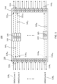
- FIG. 1 schematically illustrates an example QFSP-DD optical transceiver module 100 ("module100") having an optical interface 116 including more than four, e.g., eight, bidirectional optical data ports 112 1 , ..., 112s, commonly referred to as optical data ports 112.
- An electrical (host-side) interface 118 of the QFSP-DD optical transceiver module 100 typically includes eight bidirectional electrical data ports 114 1 , ..., 114 8 , commonly referred to as electrical data ports 114.
- the QSFP-DD optical transceiver module 100 is configured for approximately 10 Giga-bit-per-second (Gb/s) bidirectional data communication on each of the electrical data ports 114 and each of the optical data ports 112.
- approximately 10Gb/s means that the actual bit rate of data signals transmitted through the port may slightly differ from 10Gb/s, typically within + ⁇ - 1Gb/s, or possibly up to + ⁇ -2Gb/s, e.g. due to a coding overhead or circuit tolerances.
- the QSFP-DD optical transceiver module 100 may be configured to support up to 8 independent 10 Gigabit Ethernet (GbE) channels between the optical and electrical interfaces thereof.
- the nominal transmission bit rate (“line rate” in this example may be about 10.3125Gb/s ("10GBASE-R" line rate) due to a 64/66 PCS (Physical Coding Sublayer) encoding.
- the line rate supported by the QSFP-DD optical transceiver module 100 may be 9.95328 Gb/s ("10GBASE-W"); other line rates may be used for near-lOG communications employing e.g. Fibre Channel, InfiniBand, or SONET/SDH communication formats.
- 10 Gb/s may be abbreviated as “10Gb/s”, which is to be understood as including the word "approximately”.
- the eight electrical data ports 114 1 ,...,114 8 are duplex ports configured to connect to corresponding duplex bidirectional electrical 10G lanes 128 1 ,...,128 8 ("lOG lanes 128") of a host device, e.g. a data router or switch, via signal-receiving (Rx) and signal-transmitting (Tx) electrical connectors 114 Rx , 114 Tx .
- a host device e.g. a data router or switch
- Rx signal-receiving
- Tx signal-transmitting
- Each of the 10G lanes 128 may be a duplex electrical lane where the Rx and Tx signals propagate along different electrical lines.
- Each of the bidirectional optical data ports 112 is, in the shown example, a duplex port including a Tx optical connector 112 TX and an Rx optical connector 112 RX , for connecting to corresponding optical fibers of a full-duplex optical communication link (not shown) with different fibers for Tx and Rx optical signals.
- the Rx and Tx connectors 114 RX and 114 TX of a same bidirectional, full-duplex in the shown example, electrical data port 114 may or may not be located side by side as schematically illustrated in FIGs.
- all of the electrical Rx connectors 114 RX may be grouped at one side of the electrical interface 118, and all of the electrical Tx connectors 114 TX may be grouped at another side of the electrical interface 118.
- the optical Rx and Tx connectors 112 RX and 112 TX of a same full-duplex optical data port 112 may or may not be located side by side as schematically illustrated in FIGs. 1 and 2 ; for example, in some implementations all of the optical Rx connectors 112 RX (e.g. ferrules) may be grouped at one side of the optical interface 116, and all of the optical Tx connectors 112 TX (e.g. ferrules) may be grouped at another side of the optical interface 116.
- At least some of the optical data ports 112 may each use a single optical connector, commonly referred to as "BiDi", to receive and transmit optical signals from a same optical fiber.
- at least some of the electrical data ports 114 may each be a "BiDi" electrical port configured to receive and transmit electrical signals from a same "BiDi" electrical lane 128.
- the QSFP-DD optical transceiver module 100 is configured to communicatively pair-wise inter-connect, or "map", each one of the optical data ports 112 thereof to a corresponding one of the electrical data ports 114, at a data rate of approximately 10 Gb/s for each of the port-to-port connections.
- the QSFP-DD optical transceiver module 100 is configured to pair-wise connect eight optical data ports 112 to corresponding ones of the electrical data ports 114 at approximately 10 Gb/s data rate per connection, to provide eight full-duplex 10GB/s data paths 141 1 , ..., 141 8 ("data paths 141") between the optical and electrical interfaces 116, 118.
- Each of the data paths 114 includes a 10Gb/s electrical-to-optical (E/O) converter 144 in an optical Tx path and a 10Gb/s optical-to-electrical (O/E) converter 145 in an optical Rx path.
- the 10 Gb/s E/O converter 144 may include a laser source (not shown) configured to be modulated at approximately 10Gb/s bit rate, e.g. a semiconductor laser chip incorporating an electro-absorption modulator (EML), and a corresponding laser driver (not shown) configured to generate 10Gb/s modulation signals.
- EML electro-absorption modulator
- the driver may include a digital-to-analog converter ("DAC", not shown) to convert a received 10Gb/s digital signal into an analog electrical signal to drive the laser.
- the 10 Gb/s O/E converter 145 may include a photodetector (not shown), e.g. a PIN diode, coupled to a transimpedance amplifier (TIA) (not shown), each of which configured to operate on signals at approximately 10Gb/s bit rate.
- the O/E converter may include an analog-to-digital converter ("ADC", not shown) to digitize the output signal of the TIA for transmission at the corresponding electrical Tx connector.
- ADC analog-to-digital converter
- Variations of the QSFP-DD optical transceiver module 100 may include more than four, e.g. 5, 6, 7, or 8 bi-directional, e.g. duplex, optical data ports 112, and an equal number, e.g. 5, 6, 7, or 8, bidirectional, e.g. duplex, electrical data ports 114.
- the optical (116) and electrical (118) interfaces of the module may be interconnected by more than four, e.g. 5, 6, 7, or 8 separate bidirectional, e.g. duplex, data paths 141, each of which configured for approximately 10 Gb/s line rates.
- the QSFP-DD optical transceiver module 100 does not have re-timing or clock-and-data (CDR) circuitry in any of the 10G data path 141, although embodiments including such circuitry may also be contemplated.
- CDR clock-and-data
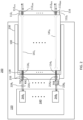
- FIG. 2 illustrates an apparatus 200, such as digital data router or switch, including a host device 220 configured for use with the QSFP-DD optical transceiver module(s) 100.
- the host device 220 may be, e.g., a card or a circuit board configured to be installed in the apparatus 200.
- the host device 220 has at least one receptacle 230, which may also be referred to as a cage, configured for receiving the QSFP-DD optical transceiver module 100.
- the receptacle 230 includes an electrical interface 233 having eight bidirectional electrical data ports 214 1 , .., 214 8 ("electrical data ports 214"), at least five of said electrical data ports 214 being configured for simultaneous bidirectional data communication, at a rate of approximately 10 Giga-bit-per-second (Gb/s) per port, between the host device 220 and a QSFP-DD optical transceiver module plugged into the receptacle 230, e.g. the QSFP-DD optical transceiver module 100.
- the host device 220 may include a PHY layer device 240, e.g.
- DSP digital signal processor
- ASIC application specific integrated circuit
- Each of the clock recovery circuits 244 may be configured to detect a clock, or reference, frequency for a data signal received from the QSFP-DD optical transceiver module 100 over a corresponding one of the electrical lanes 228, and to sample the received signal at the detected clock frequency.
- each clock recovery circuit 244 includes a phase locked loop (PLL) circuit (not shown) dedicated to locking on a frequency of the electrical data signal received over a corresponding electrical lane 228. This allows each of the 5, 6, 7, or 8 electrical lanes 228 to run on independent clock reference frequencies.
- PLL phase locked loop
- a 10GbE signal may have a bit rate within a band of +/- 100ppm (parts per million).
- a data signal received over one of the electrical data lanes 228, e.g. lane 228 1 may have a line rate of (10GbE - 100ppm), while a data signal received over another one of the electrical data lanes 228, e.g. lane 228 8 , may have a line rate of (10GbE + 100ppm).
- These clock frequencies corresponding to these two line rates are not identical, therefore a separate PLL circuit may be used for each electrical lane 228, so that each lane 228 of the host device 220 may operate at the line rate of a corresponding one of the electrical ports 114 / data path 141 of the QSFP-DD optical transceiver module 100.
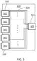
- FIG. 3 illustrates an example digital data router or switch 300 configured to use one or more QSFP-DD optical transceiver modules as described above to aggregate the data from a plurality of 10GbE channels thereof into one or more higher data rate channels.
- the digital data router 300 has a plurality of QSFP-DD receptacles 310, five in the illustrated example, each receptacle 310 having N bi-directional 10GbE electrical lanes for connecting to N ⁇ 10GbE electrical ports of a QSFP-DD optical transceiver module 301 plugged therein.
- N is an integer greater than 4, e.g. 5, 6, 7, or 8.
- the QSFP-DD optical transceiver module 301 may be an embodiment of the QSFP-DD optical transceiver module 100 described above.
- the digital data router 300 further includes a QSFP-DD receptacle 311 having M ⁇ 1 bidirectional, e.g. duplex, electrical ports, each configured for e.g. N ⁇ 10 GbE data rate.
- the digital data router 300 includes a packet processor 320, e.g. an ASIC, configured to aggregate N 10 GbE signal channels into a N ⁇ 10 GbE channel.
- the QSFP-DD optical transceiver modules 305, and the corresponding QSFP-DD receptacle 311, has eight 50G electrical ports to support a 400 GbE data channel.
- the packet processor 320 is configured to aggregate the data from forty 10 GbE data channels of the QSFP-DD optical transceiver modules 301 into a 400 GbE data channel of the QSFP-DD optical transceiver module 305.
- the examples describe above allow to combine a full support for Synchronous Ethernet with a high 10 GbE port density without the need for an MLG support either at the router or the pluggable optical module.
- the prior-art 10x10G MLG approach described above can only run the 4x25G electrical lanes at one frequency, which also defines the reference frequency for each of 10x10GbE optical ports
- the QSFP-DD optical transceiver modules configured for 8x10GbE breakout allow supporting eight independent 10 GbE channels, i.e., 8 separate bidirectional channels without data mixing therebetween, wherein each channel synchronized to a different clock within the allowable range for 10GbE, both on the optical and electrical interfaces.
- optical componentry i.e. lasers, photodetectors, etc.
- Other potential advantages include low power consumption, easier thermal management, and lower module complexity, e.g. simpler circuitry, less firmware and software, greater reliability.
- an apparatus e.g. 100, FIG. 1 ; 200, FIG. 2 ; 300, FIG. 3 , comprising a Quad Small Form-Factor Pluggable Double Density (QSFP-DD) optical transceiver module (e.g. 100, FIGs. 1 , 2 ; 301, FIG. 3 ) having more than four bidirectional optical data ports (e.g. 112 1 , 112 8 , FIGs. 1 , 2 ) and more than four bidirectional electrical data ports (e.g. 114 1 ,114 8 , FIGs.
- QSFP-DD Quad Small Form-Factor Pluggable Double Density
- the QSFP-DD optical transceiver module is configured for approximately 10 giga-bit-per-second (Gb/s) bidirectional data communication on each of the data ports (e.g. 114, 112); and wherein the QSFP-DD optical transceiver module is configured to communicatively inter-connect each optical data port thereof (e.g. 112 1 ) to a corresponding one of the electrical data ports (e.g. 114 1 ) thereof.
- Gb/s giga-bit-per-second
- the QSFP-DD optical transceiver module (e.g. 100, FIGs. 1 , 2 ; 301, FIG. 3 ) is configured to inter-connect each of the optical data ports thereof to the corresponding one of the electrical data ports thereof at an approximately 10 Gb/s data rate.
- each of said optical (e.g. 112, FIGs. 1 , 2 ) and electrical (e.g. 114, FIGs. 1 , 2 ) data ports is full-duplex.
- the QSFP-DD optical transceiver module (e.g. 100, FIGs. 1 , 2 ; 301, FIG. 3 ) is configured to communicate data between each one of the pairs of corresponding electrical and optical data ports of the module without mixing therein of data from another of the pairs of corresponding electrical and optical data ports of the module.
- the QSFP-DD optical transceiver module (e.g. 100, FIGs. 1 , 2 ; 301, FIG. 3 ) is absent of CDR circuitry.
- any of the above apparatus (e.g. 200, FIG. 2 ; 300, FIG. 3 ) further comprise a digital data router or switch (e.g. 210, FIG. 2 ; 300, FIG. 3 ) having a plurality of receptacles (e.g. 230, FIG. 2 ; 310, FIG. 3 ) for QSFP-DD modules, the QSFP-DD optical transceiver module (e.g. 100, FIG. 2 ; 301, FIG.
- a digital data router or switch e.g. 210, FIG. 2 ; 300, FIG. 3
- a plurality of receptacles e.g. 230, FIG. 2 ; 310, FIG. 3
- the QSFP-DD optical transceiver module e.g. 100, FIG. 2 ; 301, FIG.
- the digital data router or switch is configured for parallel data communication with the QSFP-DD optical transceiver module over the more than four electrical data ports of the one of the receptacles at a rate of approximately 10 Gb/s per port and direction.
- the digital data router or switch is configured to provide clock recovery (e.g. 244 1 , 244 8 , FIG. 2 ) at approximately 10Gb/s bit rate for data signals received from each of the more than four electrical data ports (e.g. 214 1 , 214 8 , FIG. 2 ) of the one of the receptacles (e.g. 230, FIG. 2 ) thereof.
- the QSFP-DD optical transceiver module comprises more than four separate bidirectional data links (e.g. 141, FIGs. 1 and 2 ) pair-wise interconnecting the electrical and optical data ports thereof, each of the separate bidirectional data links comprising an electrical-to-optical converter (e.g. 144, FIG. 1 ) configured for approximately 10Gb/s operation.
- each of the separate bidirectional data links may further comprise an optical-to-electrical converter (e.g. 145, FIG. 1 ) configured for approximately 10Gb/s operation.
- the QSFP-DD optical transceiver module (e.g. 100, FIGs. 1 , 2 ; 301, FIG. 3 ) has, at least, six of the optical data ports and at least six of the electrical data ports, each of said at least six of the optical data ports and said at least of the electrical data ports being configured for full-duplex operation at an approximately 10 Gb/s data rate.
- a digital data router or switch e.g.
- the QSFP-DD optical transceiver module is plugged in one of the receptacles having at least six electrical data ports; the digital data router or switch is configured for parallel data communication with the QSFP-DD optical transceiver module over the more than six electrical data ports of the one of the receptacles, at a rate of approximately 10 Gb/s per port in each direction.
- the QSFP-DD optical transceiver module has eight of the optical data ports and eight of the electrical data ports, each of said eight of the electrical ports being configured for full-duplex operation at approximately 10 Gb/s data rate.
- Some of such embodiments further comprise a digital data router or switch having a plurality of receptacles for QSFP-DD optical transceiver modules, the QSFP-DD optical transceiver module being plugged in one of the receptacles having eight electrical data ports; the digital data router or switch may be configured for parallel data communication with the QSFP-DD optical transceiver module over the eight electrical data ports of the one of the receptacles, at a rate of approximately 10 Gb/s per port and direction.
- the QSFP-DD optical transceiver module is configured for an 8x10 gigabit Ethernet (GbE) break-out.
- GbE gigabit Ethernet
- the QSFP-DD optical transceiver module is configured to support bidirectional 10 gigabit Ethernet (GbE) communications between each of the more than 4 optical data ports thereof and a corresponding one of the electrical data ports thereof.
- GbE gigabit Ethernet
- an apparatus (200, FIG. 2 ; 300, FIG. 3 ).
- the apparatus comprises a digital data router or switch (e.g. 200, FIG. 2 ; 300, FIG. 3 ) comprising a plurality of receptacles (e.g. 230, FIG. 2 ; 310, FIG. 3 ) for QSFP-DD optical modules, one of the receptacles having eight electrical data ports (e.g. 214 1 - 214 8 , FIG. 2 ).
- the digital data router or switch is configured for parallel bidirectional data communication with a QSFP-DD optical transceiver module (e.g. 100) plugged into the one of the receptacles (e.g. 230) over at least five of the eight electrical data ports at a rate of approximately 10 Gb/s per port.
- the apparatus comprises a dedicated clock recovery circuit (e.g. 244 1 , 244 8 , FIG. 2 ) for each of the at least five electrical data ports, each of the dedicated clock recovery circuits configured for approximately 10 Gb/s signal bit rate.
- the apparatus comprises a dedicated clock recovery circuit (e.g. 244 1 - 244 s ) for each of the eight electrical data ports, each of the dedicated clock recovery circuits configured for approximately 10 Gb/s signal bit rate.
- figure numbers and/or figure reference labels in the claims is intended to identify one or more possible embodiments of the claimed subject matter in order to facilitate the interpretation of the claims. Such use is not to be construed as necessarily limiting the scope of those claims to the embodiments shown in the corresponding figures.
Landscapes
- Physics & Mathematics (AREA)
- Electromagnetism (AREA)
- Engineering & Computer Science (AREA)
- Computer Networks & Wireless Communication (AREA)
- Signal Processing (AREA)
- General Physics & Mathematics (AREA)
- Optics & Photonics (AREA)
- Optical Communication System (AREA)
Abstract
A QSFP-DD optical transceiver module having more than four optical data ports and more than four electrical data ports is configured for approximately 10 Gb/s bidirectional data communication on each of the data ports, and is further configured to communicatively interconnect each of the optical data ports thereof to a corresponding one of the electrical data ports thereof. The module may be used with a digital data router or switch having at least one QSFP-DD receptacle with eight electrical data ports and configured for parallel bidirectional communication with the QSFP-DD module plugged therein over at least five of the eight electrical data ports at 10 Gb/s per port and direction.
Description
- The present invention relates to pluggable optical transceiver modules for broad-band optical communications and data centers.
- Data routers in broad-band telecom networks and data centers typically use pluggable optical transceiver modules to convert between electrical signals (e.g. host-side) and optical signals (e.g. line-side or client-side). The optical signals are transmitted via fiber optic cables to interconnect with other routers or switches. Pluggable optical transceiver modules may have different form factors, which are typically governed by corresponding Multi Source Agreements (MSA) between various equipment manufacturers and system providers. In response to the market requirements of ever increasing bandwidth, each next generation of such modules has been developed to support a greater data rate per port. Examples of such modules include SFP (Small Form-factor Pluggable) and QSFP (Quad Small Form-factor Pluggable) modules, each of which with several modifications evolved to use ever increasing data rates. E.g. the QSFP standard has evolved from an aggregate port speed of 40 Giga-bit-per-second (Gb/s) to 400Gb/s over the years. The host-side interface of various QSFP flavors supports 4 (four) electrical lanes running at 4x10G (QSFP+), 4x25G (QSFP28), 4x50G (QSFP56), or 4x100G (QSFP112). Here "G" stands for a data rate of approximately 1 Gb/s, in accordance with a common convention. The electrical lanes at the host-side interface can be aggregated into large Ethernet optical ports, e.g. a QSFP28 module can aggregate 4x25G electrical signals into a 100GbE (Gigabit Ethernet) optical port, or can be unaggregated ("break out") and connected to individual optical transmitters/receivers, e.g. 4x25G electrical signals into 4x25GbE independent optical ports.
- The QSFP-DD (i.e. QSFP Double-Density) optical transceiver modules have been developed to double the number of electrical lanes to 8 (eight), with the aggregated port data rates 8x25G ("QSFP28-DD", or "QSFP-DD200"), 8x50G ("QSFP56-DD", or "QSFP-DD400"), and 8x100G ("QSFP112-DD", or "QSFP-DD800"). The QSFP-DD cage (i.e. the host-side receptacle for the pluggable module) was designed for backwards compatibility with 4-lane QSFP modules.
- An example embodiment described herein provides an apparatus comprising a Quad Small Form-Factor Pluggable Double Density (QSFP-DD) optical transceiver module having more than 4 bidirectional optical data ports and more than 4 bidirectional electrical data ports. The QSFP-DD optical transceiver module is configured for approximately 10 Giga-bit-per-second (Gb/s) bidirectional data communication on each of the data ports. The QSFP-DD optical transceiver module is further configured to communicatively inter-connect each optical data port thereof to a corresponding one of the electrical data ports thereof.
- A related example described herein provides an apparatus comprising a digital data router or switch. The digital data router or switch comprises a plurality of receptacles for Quad Small Form-Factor Pluggable Double Density (QSFP-DD) optical transceiver modules. Each one of the receptacles has eight electrical data ports, at least five of the eight electrical data ports being configured for simultaneous bidirectional data communication, at a rate of approximately 10 Giga-bit-per-second (Gb/s) for each port, between the digital data router or switch and a QSFP-DD module plugged into the one of the receptacles.
- Embodiments disclosed herein will be described in greater detail with reference to the accompanying drawings which represent preferred embodiments thereof, in which like elements are indicated with like reference numerals, and wherein:
-
FIG. 1 is a schematic diagram illustrating a QSFP-DD optical transceiver module configured for 8x10G break-out; -
FIG. 2 is a schematic diagram illustrating a host device configured to communicate with QSFP-DD optical transceiver modules of the type shown inFIG. 1 ; -
FIG. 3 is a schematic diagram illustrating a digital data router configured to host, and aggregate the data from, a plurality of 10GbE electrical data ports of one or more QSFP-DD optical transceiver modules ofFIG. 1 . - In the following description, for purposes of explanation and not limitation, specific details are set forth, such as particular circuits, circuit components, techniques, etc. in order to provide a thorough understanding of the present invention. However, it will be apparent to one skilled in the art that the present invention may be practiced in other embodiments that depart from these specific details. In other instances, detailed descriptions of well-known methods, devices, and circuits may be omitted so as not to obscure the description of the present invention. All statements herein reciting principles, aspects, and embodiments of the invention, as well as specific examples thereof, are intended to encompass both structural and functional equivalents thereof. Additionally, it is intended that such equivalents include both currently known equivalents as well as equivalents developed in the future, i.e., any elements developed that perform the same function, regardless of structure.
- Note that as used herein, the terms "first", "second" and so forth are not intended to imply sequential ordering, but rather are intended to distinguish one element from another, unless explicitly stated. Similarly, sequential ordering of method steps does not imply a requirement of sequential order of their execution, unless explicitly stated.
- The following abbreviations and acronyms may be used in the present document:
- ADC: Analog to Digital Converter
- DAC: Digital to Analog Converter
- QSFP: Quad Small Form-Factor Pluggable
- QSFP-DD: QSFP Double-Density
- MSA: Multi Source Agreement
- MPO: Multi-Fiber Push On
- MLG: Multi-link Gearbox
- GbE: Gigabit Ethernet
- PHY: Physical Layer
- PAM4: Pulse Amplitude Modulation, 4 level
- ASIC: Application-Specific Integrated Circuit
- TIA: Transimpedance Amplifier
- Designers of broad-band telecom systems and data centers may source pluggable optical transvers modules from different manufacturers. In order to ensure interoperability, such modules are typically governed by MSAs that define requirements to form-factors and electrical, optical, mechanical, and control interfaces of such modules. In response to the market demands of ever increasing bandwidth, each next generation of such modules has been developed to support a greater data rate per port. E.g. the QSFP family of modules, having four electrical lines, have evolved over the years from supporting a data rate of approximately 10-40 Gb/s per port (QSFP+ modules), to 25-100 Gb/s per port (QSFP28 modules), with even greater rates possible with PAM4 modulation formats. To meet the market need for modules with high aggregated data rates of 400G and 800G, QSFP-DD (i.e. QSFP Double-Density) optical transceiver modules have been developed to double the number of electrical lanes to 8 (eight), with data rate per electrical lane or port of 25G, 50G, or 100G, and the aggregated port rate of 200G, 400G, or 800G (QSFP-DD800).
- However, client-side data channels still frequently operate at data rates of about 10Gb/s (due to the ubiquity of 10G SFP+), and digital data routers or switches having an ability to aggregate a large number of such channels in a relatively small footprint are desired. One existing solution is a QSFP28 optical transceiver module that has a 4-lane, 25G per lane host-side electrical interface and 10 independent 10GbE client-side optical ports. This optical transceiver module relies on an MLG (Multi-link Gearbox) protocol to convert between the 10GbE optical signals and a 100G (i.e. 4x25G) electrical channel, and requires an MLG gearbox device inside the optical transceiver module, which adds to power supply requirements, cost, and complexity of the module. It also requires the host router's Physical Layer (PHY) device to have MLG functionality, which is not widely supported by typical Ethernet PHY/ devices currently on the market.
- The present disclosure describes examples of a QSFP-DD optical transceiver module configured for N×10G breakout, where N is greater than 4, e.g. 5, 6, 7, or 8; this allows increasing, e.g., the 10GbE "break out" port density on routers and switches without the drawbacks of a 10x10GbE MLG solution.
-
FIG. 1 schematically illustrates an example QFSP-DD optical transceiver module 100 ("module100") having anoptical interface 116 including more than four, e.g., eight, bidirectional optical data ports 1121, ..., 112s, commonly referred to as optical data ports 112. An electrical (host-side)interface 118 of the QFSP-DDoptical transceiver module 100 typically includes eight bidirectional electrical data ports 1141, ..., 1148, commonly referred to as electrical data ports 114. The QSFP-DDoptical transceiver module 100 is configured for approximately 10 Giga-bit-per-second (Gb/s) bidirectional data communication on each of the electrical data ports 114 and each of the optical data ports 112. - Here, "approximately 10Gb/s" means that the actual bit rate of data signals transmitted through the port may slightly differ from 10Gb/s, typically within +\- 1Gb/s, or possibly up to +\-2Gb/s, e.g. due to a coding overhead or circuit tolerances. For example, the QSFP-DD
optical transceiver module 100 may be configured to support up to 8 independent 10 Gigabit Ethernet (GbE) channels between the optical and electrical interfaces thereof. The nominal transmission bit rate ("line rate" in this example may be about 10.3125Gb/s ("10GBASE-R" line rate) due to a 64/66 PCS (Physical Coding Sublayer) encoding. In another example, the line rate supported by the QSFP-DDoptical transceiver module 100 may be 9.95328 Gb/s ("10GBASE-W"); other line rates may be used for near-lOG communications employing e.g. Fibre Channel, InfiniBand, or SONET/SDH communication formats. In the following "approximately 10 Gb/s" may be abbreviated as "10Gb/s", which is to be understood as including the word "approximately". - In the example illustrated in
FIG. 1 , the eight electrical data ports 1141,...,1148 are duplex ports configured to connect to corresponding duplex bidirectional electrical 10G lanes 1281,...,1288 ("lOG lanes 128") of a host device, e.g. a data router or switch, via signal-receiving (Rx) and signal-transmitting (Tx) electrical connectors 114Rx, 114Tx. Each of the 10G lanes 128 may be a duplex electrical lane where the Rx and Tx signals propagate along different electrical lines. Each of the bidirectional optical data ports 112 is, in the shown example, a duplex port including a Tx optical connector 112TX and an Rx optical connector 112RX, for connecting to corresponding optical fibers of a full-duplex optical communication link (not shown) with different fibers for Tx and Rx optical signals. The Rx and Tx connectors 114RX and 114TX of a same bidirectional, full-duplex in the shown example, electrical data port 114 may or may not be located side by side as schematically illustrated inFIGs. 1 and2 ; for example, in some embodiments all of the electrical Rx connectors 114RX may be grouped at one side of theelectrical interface 118, and all of the electrical Tx connectors 114TX may be grouped at another side of theelectrical interface 118. Similarly, the optical Rx and Tx connectors 112RX and 112TX of a same full-duplex optical data port 112 may or may not be located side by side as schematically illustrated inFIGs. 1 and2 ; for example, in some implementations all of the optical Rx connectors 112RX (e.g. ferrules) may be grouped at one side of theoptical interface 116, and all of the optical Tx connectors 112TX (e.g. ferrules) may be grouped at another side of theoptical interface 116. - In other implementations, at least some of the optical data ports 112 may each use a single optical connector, commonly referred to as "BiDi", to receive and transmit optical signals from a same optical fiber. Similarly, in some implementations, at least some of the electrical data ports 114 may each be a "BiDi" electrical port configured to receive and transmit electrical signals from a same "BiDi" electrical lane 128.
- The QSFP-DD
optical transceiver module 100 is configured to communicatively pair-wise inter-connect, or "map", each one of the optical data ports 112 thereof to a corresponding one of the electrical data ports 114, at a data rate of approximately 10 Gb/s for each of the port-to-port connections. In the illustrated example, the QSFP-DDoptical transceiver module 100 is configured to pair-wise connect eight optical data ports 112 to corresponding ones of the electrical data ports 114 at approximately 10 Gb/s data rate per connection, to provide eight full-duplex 10GB/s data paths 1411, ..., 1418 ("data paths 141") between the optical andelectrical interfaces converter 144 in an optical Tx path and a 10Gb/s optical-to-electrical (O/E)converter 145 in an optical Rx path. The 10 Gb/s E/O converter 144 may include a laser source (not shown) configured to be modulated at approximately 10Gb/s bit rate, e.g. a semiconductor laser chip incorporating an electro-absorption modulator (EML), and a corresponding laser driver (not shown) configured to generate 10Gb/s modulation signals. In some embodiments, the driver may include a digital-to-analog converter ("DAC", not shown) to convert a received 10Gb/s digital signal into an analog electrical signal to drive the laser. The 10 Gb/s O/E converter 145 may include a photodetector (not shown), e.g. a PIN diode, coupled to a transimpedance amplifier (TIA) (not shown), each of which configured to operate on signals at approximately 10Gb/s bit rate. In some embodiments, the O/E converter may include an analog-to-digital converter ("ADC", not shown) to digitize the output signal of the TIA for transmission at the corresponding electrical Tx connector. - Variations of the QSFP-DD
optical transceiver module 100 may include more than four, e.g. 5, 6, 7, or 8 bi-directional, e.g. duplex, optical data ports 112, and an equal number, e.g. 5, 6, 7, or 8, bidirectional, e.g. duplex, electrical data ports 114. The optical (116) and electrical (118) interfaces of the module may be interconnected by more than four, e.g. 5, 6, 7, or 8 separate bidirectional, e.g. duplex, data paths 141, each of which configured for approximately 10 Gb/s line rates. - Typically, the QSFP-DD
optical transceiver module 100 does not have re-timing or clock-and-data (CDR) circuitry in any of the 10G data path 141, although embodiments including such circuitry may also be contemplated. -
FIG. 2 illustrates anapparatus 200, such as digital data router or switch, including ahost device 220 configured for use with the QSFP-DD optical transceiver module(s) 100. Thehost device 220 may be, e.g., a card or a circuit board configured to be installed in theapparatus 200. Thehost device 220 has at least onereceptacle 230, which may also be referred to as a cage, configured for receiving the QSFP-DDoptical transceiver module 100. Thereceptacle 230 includes anelectrical interface 233 having eight bidirectional electrical data ports 2141, .., 2148 ("electrical data ports 214"), at least five of said electrical data ports 214 being configured for simultaneous bidirectional data communication, at a rate of approximately 10 Giga-bit-per-second (Gb/s) per port, between thehost device 220 and a QSFP-DD optical transceiver module plugged into thereceptacle 230, e.g. the QSFP-DDoptical transceiver module 100. Thehost device 220 may include aPHY layer device 240, e.g. a digital signal processor (DSP) implemented with an ASIC, that is configured to simultaneously service and/or operate at least five, and typically up to eight, independent 10 Gb/s bidirectional, e.g. duplex, electrical lanes 2281, ..., 228s ("electrical lanes 228"), each connecting to a corresponding 10Gb/s data path 148 in the QSFP-DDoptical transceiver module 100 via theelectrical interface 233 of thereceptacle 230. The servicing and/or operating the electrical lanes 228 includes operating a corresponding clock recovery circuit 244 independently for each lane 228. The clock recovery circuits 244 may be parts of corresponding electrical data ports 214. Each of the clock recovery circuits 244 may be configured to detect a clock, or reference, frequency for a data signal received from the QSFP-DDoptical transceiver module 100 over a corresponding one of the electrical lanes 228, and to sample the received signal at the detected clock frequency. In an example embodiment, each clock recovery circuit 244 includes a phase locked loop (PLL) circuit (not shown) dedicated to locking on a frequency of the electrical data signal received over a corresponding electrical lane 228. This allows each of the 5, 6, 7, or 8 electrical lanes 228 to run on independent clock reference frequencies. By way of example, a 10GbE signal may have a bit rate within a band of +/- 100ppm (parts per million). Accordingly, a data signal received over one of the electrical data lanes 228, e.g. lane 2281, may have a line rate of (10GbE - 100ppm), while a data signal received over another one of the electrical data lanes 228, e.g. lane 2288, may have a line rate of (10GbE + 100ppm). These clock frequencies corresponding to these two line rates are not identical, therefore a separate PLL circuit may be used for each electrical lane 228, so that each lane 228 of thehost device 220 may operate at the line rate of a corresponding one of the electrical ports 114 / data path 141 of the QSFP-DDoptical transceiver module 100. -
FIG. 3 illustrates an example digital data router or switch 300 configured to use one or more QSFP-DD optical transceiver modules as described above to aggregate the data from a plurality of 10GbE channels thereof into one or more higher data rate channels. Thedigital data router 300 has a plurality of QSFP-DD receptacles 310, five in the illustrated example, eachreceptacle 310 having N bi-directional 10GbE electrical lanes for connecting to N×10GbE electrical ports of a QSFP-DDoptical transceiver module 301 plugged therein. Here N is an integer greater than 4, e.g. 5, 6, 7, or 8. The QSFP-DDoptical transceiver module 301 may be an embodiment of the QSFP-DDoptical transceiver module 100 described above. Thedigital data router 300 further includes a QSFP-DD receptacle 311 having M ≥1 bidirectional, e.g. duplex, electrical ports, each configured for e.g. N×10 GbE data rate. Thedigital data router 300 includes apacket processor 320, e.g. an ASIC, configured to aggregate N 10 GbE signal channels into a N×10 GbE channel. - In the example illustrated in
FIG. 3 , each of QSFP-DDoptical transceiver modules 301, and each of the corresponding QSFP-DD receptacles 310, has eight 10GbE electrical ports (i.e. N=8) to support 40 (forty) 10GbE data channels with a total aggregated data rate of 400G. The QSFP-DDoptical transceiver modules 305, and the corresponding QSFP-DD receptacle 311, has eight 50G electrical ports to support a 400 GbE data channel. Thepacket processor 320 is configured to aggregate the data from forty 10 GbE data channels of the QSFP-DDoptical transceiver modules 301 into a 400 GbE data channel of the QSFP-DDoptical transceiver module 305. - Advantageously, the examples describe above allow to combine a full support for Synchronous Ethernet with a high 10 GbE port density without the need for an MLG support either at the router or the pluggable optical module.
- While the prior-art 10x10G MLG approach described above can only run the 4x25G electrical lanes at one frequency, which also defines the reference frequency for each of 10x10GbE optical ports, the QSFP-DD optical transceiver modules configured for 8x10GbE breakout, as described above, allow supporting eight independent 10 GbE channels, i.e., 8 separate bidirectional channels without data mixing therebetween, wherein each channel synchronized to a different clock within the allowable range for 10GbE, both on the optical and electrical interfaces.
- Furthermore, by avoiding an MLG gearbox device inside the optical transceiver module and adopting the larger QSFP-DD form factor, there is more room inside the module for optical componentry (i.e. lasers, photodetectors, etc.). Other potential advantages include low power consumption, easier thermal management, and lower module complexity, e.g. simpler circuitry, less firmware and software, greater reliability.
- According to an example embodiment disclosed above, e.g., in the summary section and/or in reference to any one or any combination of some or all of
FIGs. 1-3 , provided is an apparatus (e.g. 100,FIG. 1 ; 200,FIG. 2 ; 300,FIG. 3 ), comprising a Quad Small Form-Factor Pluggable Double Density (QSFP-DD) optical transceiver module (e.g. 100,FIGs. 1 ,2 ; 301,FIG. 3 ) having more than four bidirectional optical data ports (e.g. 1121, 1128,FIGs. 1 ,2 ) and more than four bidirectional electrical data ports (e.g. 1141,1148,FIGs. 1 ,2 ); wherein the QSFP-DD optical transceiver module is configured for approximately 10 giga-bit-per-second (Gb/s) bidirectional data communication on each of the data ports (e.g. 114, 112); and wherein the QSFP-DD optical transceiver module is configured to communicatively inter-connect each optical data port thereof (e.g. 1121) to a corresponding one of the electrical data ports (e.g. 1141) thereof. - In some embodiments of the above apparatus, the QSFP-DD optical transceiver module (e.g. 100,
FIGs. 1 ,2 ; 301,FIG. 3 ) is configured to inter-connect each of the optical data ports thereof to the corresponding one of the electrical data ports thereof at an approximately 10 Gb/s data rate. - In some embodiments of any of the above apparatus, each of said optical (e.g. 112,
FIGs. 1 ,2 ) and electrical (e.g. 114,FIGs. 1 ,2 ) data ports is full-duplex. - In some embodiments of any of the above apparatus, the QSFP-DD optical transceiver module (e.g. 100,
FIGs. 1 ,2 ; 301,FIG. 3 ) is configured to communicate data between each one of the pairs of corresponding electrical and optical data ports of the module without mixing therein of data from another of the pairs of corresponding electrical and optical data ports of the module. - In some embodiments of any of the above apparatus, the QSFP-DD optical transceiver module (e.g. 100,
FIGs. 1 ,2 ; 301,FIG. 3 ) is absent of CDR circuitry. - Some embodiments of any of the above apparatus (e.g. 200,
FIG. 2 ; 300,FIG. 3 ) further comprise a digital data router or switch (e.g. 210,FIG. 2 ; 300,FIG. 3 ) having a plurality of receptacles (e.g. 230,FIG. 2 ; 310,FIG. 3 ) for QSFP-DD modules, the QSFP-DD optical transceiver module (e.g. 100,FIG. 2 ; 301,FIG. 3 ) plugged in one of the receptacles having more than four electrical data ports; the digital data router or switch is configured for parallel data communication with the QSFP-DD optical transceiver module over the more than four electrical data ports of the one of the receptacles at a rate of approximately 10 Gb/s per port and direction. In some of such embodiments, the digital data router or switch is configured to provide clock recovery (e.g. 2441, 2448,FIG. 2 ) at approximately 10Gb/s bit rate for data signals received from each of the more than four electrical data ports (e.g. 2141, 2148,FIG. 2 ) of the one of the receptacles (e.g. 230,FIG. 2 ) thereof. In some of such embodiments, the QSFP-DD optical transceiver module comprises more than four separate bidirectional data links (e.g. 141,FIGs. 1 and2 ) pair-wise interconnecting the electrical and optical data ports thereof, each of the separate bidirectional data links comprising an electrical-to-optical converter (e.g. 144,FIG. 1 ) configured for approximately 10Gb/s operation. In some of such embodiments, each of the separate bidirectional data links may further comprise an optical-to-electrical converter (e.g. 145,FIG. 1 ) configured for approximately 10Gb/s operation. - In some embodiments of any of the above apparatus, the QSFP-DD optical transceiver module (e.g. 100,
FIGs. 1 ,2 ; 301,FIG. 3 ) has, at least, six of the optical data ports and at least six of the electrical data ports, each of said at least six of the optical data ports and said at least of the electrical data ports being configured for full-duplex operation at an approximately 10 Gb/s data rate. In some of such embodiments comprising a digital data router or switch (e.g. having a plurality of receptacles for QSFP-DD optical transceiver modules, the QSFP-DD optical transceiver module is plugged in one of the receptacles having at least six electrical data ports; the digital data router or switch is configured for parallel data communication with the QSFP-DD optical transceiver module over the more than six electrical data ports of the one of the receptacles, at a rate of approximately 10 Gb/s per port in each direction. - In some embodiments of any of the above apparatus, the QSFP-DD optical transceiver module has eight of the optical data ports and eight of the electrical data ports, each of said eight of the electrical ports being configured for full-duplex operation at approximately 10 Gb/s data rate. Some of such embodiments further comprise a digital data router or switch having a plurality of receptacles for QSFP-DD optical transceiver modules, the QSFP-DD optical transceiver module being plugged in one of the receptacles having eight electrical data ports; the digital data router or switch may be configured for parallel data communication with the QSFP-DD optical transceiver module over the eight electrical data ports of the one of the receptacles, at a rate of approximately 10 Gb/s per port and direction.
- In some embodiments of any of the above apparatus, the QSFP-DD optical transceiver module is configured for an 8x10 gigabit Ethernet (GbE) break-out.
- In some embodiments of any of the above apparatus, the QSFP-DD optical transceiver module is configured to support bidirectional 10 gigabit Ethernet (GbE) communications between each of the more than 4 optical data ports thereof and a corresponding one of the electrical data ports thereof.
- According to a related example embodiment disclosed above, e.g., in the summary section and/or in reference to any one or any combination of some or all of
FIGs. 1-3 , provided is an apparatus (200,FIG. 2 ; 300,FIG. 3 ). The apparatus comprises a digital data router or switch (e.g. 200,FIG. 2 ; 300,FIG. 3 ) comprising a plurality of receptacles (e.g. 230,FIG. 2 ; 310,FIG. 3 ) for QSFP-DD optical modules, one of the receptacles having eight electrical data ports (e.g. 2141 - 2148,FIG. 2 ). The digital data router or switch is configured for parallel bidirectional data communication with a QSFP-DD optical transceiver module (e.g. 100) plugged into the one of the receptacles (e.g. 230) over at least five of the eight electrical data ports at a rate of approximately 10 Gb/s per port. According to some embodiments, the apparatus comprises a dedicated clock recovery circuit (e.g. 2441, 2448,FIG. 2 ) for each of the at least five electrical data ports, each of the dedicated clock recovery circuits configured for approximately 10 Gb/s signal bit rate. According to some of such embodiments, the apparatus comprises a dedicated clock recovery circuit (e.g. 2441 - 244s) for each of the eight electrical data ports, each of the dedicated clock recovery circuits configured for approximately 10 Gb/s signal bit rate. - The above described examples of the pluggable optical transceiver module for N×10Gb/s bidirectional ports at each of the optical and electrical interfaces thereof, where N>4, and of the digital data router configured for such pluggable modules, are not intended to be limiting, and many variations will become apparent to a skilled reader having the benefit of the present disclosure.
- Unless explicitly stated otherwise, each numerical value and range should be interpreted as being approximate as if the word "about" or "approximately" preceded the value or range.
- It will be further understood that various changes in the details, materials, and arrangements of the parts which have been described and illustrated in order to explain the nature of this disclosure may be made by those skilled in the art without departing from the scope of the disclosure, e.g., as expressed in the following claims. Various features described above with reference to a specific embodiment or embodiments may be combined with other embodiments.
- The use of figure numbers and/or figure reference labels in the claims is intended to identify one or more possible embodiments of the claimed subject matter in order to facilitate the interpretation of the claims. Such use is not to be construed as necessarily limiting the scope of those claims to the embodiments shown in the corresponding figures.
- Reference herein to "one embodiment" or "an embodiment" means that a particular feature, structure, or characteristic described in connection with the embodiment can be included in at least one embodiment of the disclosure. The appearances of the phrase "in one embodiment" in various places in the specification are not necessarily all referring to the same embodiment, nor are separate or alternative embodiments necessarily mutually exclusive of other embodiments. The same applies to the term "implementation."
- Furthermore in the description above, for purposes of explanation and not limitation, specific details are set forth such as particular architectures, interfaces, techniques, etc. in order to provide a thorough understanding of the present invention. In some instances, detailed descriptions of well-known devices, circuits, and methods are omitted so as not to obscure the description of the present invention with unnecessary detail. Thus, for example, it will be appreciated by those skilled in the art that block diagrams herein can represent conceptual views of illustrative circuitry embodying the principles of the technology. All statements herein reciting principles, aspects, and embodiments of the invention, as well as specific examples thereof, are intended to encompass both structural and functional equivalents thereof. Additionally, it is intended that such equivalents include both currently known equivalents as well as equivalents developed in the future, i.e., any elements developed that perform the same function, regardless of structure.
- Thus, while the present invention has been particularly shown and described with reference to example embodiments as illustrated in the drawing, it will be understood by one skilled in the art that various changes in detail may be affected therein without departing from the spirit and scope of the invention as defined by the claims.
Claims (14)
- An apparatus comprising:a Quad Small Form-Factor Pluggable Double Density (QSFP-DD) optical transceiver module comprising more than four optical data ports and more than four electrical data ports;wherein the QSFP-DD optical transceiver module is configured for approximately 10 giga-bit-per-second (Gb/s) bidirectional data communication on each of the data ports; andwherein the QSFP-DD optical transceiver module is configured to communicatively inter-connect each of the optical data ports thereof to a corresponding one of the electrical data ports thereof.
- The apparatus of claim 1, wherein the QSFP-DD optical transceiver module is configured to inter-connect each of the optical data ports thereof to the corresponding one of the electrical data ports thereof at an approximately 10 Gb/s data rate.
- The apparatus of claim 2, wherein each of said optical and electrical data ports is full-duplex.
- The apparatus of claim 3, wherein the QSFP-DD optical transceiver module is absent of CDR circuitry.
- The apparatus of claim 3, wherein the QSFP-DD optical transceiver module is configured to communicate data between pairs of corresponding electrical and optical data ports of the module without mixing therein of data from another of the pairs of corresponding electrical and optical data ports of the module.
- The apparatus of claim 2, further comprising a digital data router or switch having a plurality of receptacles for QSFP-DD modules, the QSFP-DD optical transceiver module being plugged into one of the receptacles having more than four electrical data ports;
wherein the digital data router or switch is configured for parallel data communication with the QSFP-DD optical transceiver module over the more than four electrical data ports of the one of the receptacles at a rate of approximately 10 Gb/s per port. - The apparatus of claim 6, wherein the digital data router or switch is configured to provide clock recovery at approximately 10Gb/s bit rate for data signals received from each of the more than four electrical data ports of the one of the receptacles thereof.
- The apparatus of claim 6, wherein the QSFP-DD optical transceiver module comprises more than four separate bidirectional data links pair-wise interconnecting the electrical and optical data ports thereof, each of the separate bidirectional data links comprising an electrical-to-optical converter configured for approximately 10Gb/s operation.
- The apparatus of claim 8, wherein each of the separate bidirectional data links further comprises an optical-to-electrical converter configured for approximately 10Gb/s operation.
- The apparatus of claim 2, wherein the QSFP-DD optical transceiver module has eight of the optical data ports and eight of the electrical data ports, each of said eight of the electrical ports being configured for full-duplex operation at approximately 10 Gb/s data rate.
- The apparatus of claim 10, further comprising a digital data router or switch having a plurality of receptacles for QSFP-DD modules, the QSFP-DD optical transceiver module being plugged into one of the receptacles having eight electrical data ports, wherein the digital data router or switch is configured for parallel data communication with the QSFP-DD optical transceiver module over the eight electrical data ports of the one of the receptacles at a rate of approximately 10 Gb/s per port.
- The apparatus of claim 10, wherein the QSFP-DD optical transceiver module is configured for an 8x10 gigabit Ethernet (GbE) break-out.
- The apparatus of claim 2, wherein the QSFP-DD optical transceiver module is configured to support bidirectional 10 gigabit Ethernet (GbE) communications between each of the more than 4 optical data ports thereof and a corresponding one of the electrical data ports thereof.
- The apparatus of claim 11, wherein the digital data router or switch is configured for 10 gigabit Ethernet (GbE) communications on each of the eight electrical data ports of the one of the receptacles.
Applications Claiming Priority (1)
| Application Number | Priority Date | Filing Date | Title |
|---|---|---|---|
| US18/205,269 US12556281B2 (en) | 2023-06-02 | 2023-06-02 | Pluggable optical transceiver module |
Publications (1)
| Publication Number | Publication Date |
|---|---|
| EP4475461A1 true EP4475461A1 (en) | 2024-12-11 |
Family
ID=91193640
Family Applications (1)
| Application Number | Title | Priority Date | Filing Date |
|---|---|---|---|
| EP24177015.5A Pending EP4475461A1 (en) | 2023-06-02 | 2024-05-21 | Pluggable optical transceiver module |
Country Status (3)
| Country | Link |
|---|---|
| US (1) | US12556281B2 (en) |
| EP (1) | EP4475461A1 (en) |
| CN (1) | CN119070913A (en) |
Families Citing this family (1)
| Publication number | Priority date | Publication date | Assignee | Title |
|---|---|---|---|---|
| US12598050B2 (en) * | 2023-07-06 | 2026-04-07 | Nvidia Corporation | Two-way transceiver encoding for simultaneous bidirectional signaling |
Citations (2)
| Publication number | Priority date | Publication date | Assignee | Title |
|---|---|---|---|---|
| US20210119835A1 (en) * | 2019-12-04 | 2021-04-22 | Intel Corporation | Transceiver parameter determination |
| US11385426B2 (en) * | 2021-03-09 | 2022-07-12 | Arista Networks, Inc. | Pluggable optics module with octal SN or MDC sockets |
Family Cites Families (2)
| Publication number | Priority date | Publication date | Assignee | Title |
|---|---|---|---|---|
| US10150245B2 (en) | 2008-11-11 | 2018-12-11 | University Of Florida Research Foundation, Inc. | Method of patterning a surface and articles comprising the same |
| US10742513B2 (en) * | 2018-02-05 | 2020-08-11 | David I-Keong Wong | Network interconnect as a switch |
-
2023
- 2023-06-02 US US18/205,269 patent/US12556281B2/en active Active
-
2024
- 2024-05-21 EP EP24177015.5A patent/EP4475461A1/en active Pending
- 2024-05-30 CN CN202410692180.8A patent/CN119070913A/en active Pending
Patent Citations (2)
| Publication number | Priority date | Publication date | Assignee | Title |
|---|---|---|---|---|
| US20210119835A1 (en) * | 2019-12-04 | 2021-04-22 | Intel Corporation | Transceiver parameter determination |
| US11385426B2 (en) * | 2021-03-09 | 2022-07-12 | Arista Networks, Inc. | Pluggable optics module with octal SN or MDC sockets |
Non-Patent Citations (2)
| Title |
|---|
| CYRIEL MINKENBERG ET AL: "Co-packaged datacenter optics: Opportunities and challenges", IET OPTOELECTRONICS, THE INSTITUTION OF ENGINEERING AND TECHNOLOGY, MICHAEL FARADAY HOUSE, SIX HILLS WAY, STEVENAGE, HERTS. SG1 2AY, UK, vol. 15, no. 2, 22 March 2021 (2021-03-22), pages 77 - 91, XP006109674, ISSN: 1751-8768, DOI: 10.1049/OTE2.12020 * |
| PIEHLER DAVID: "Optical interconnects in enterprise and hyperscale datacenters", SPIE PROCEEDINGS; [PROCEEDINGS OF SPIE ISSN 0277-786X], SPIE, US, vol. 11286, 28 February 2020 (2020-02-28), pages 1128602 - 1128602, XP060129069, ISBN: 978-1-5106-3673-6, DOI: 10.1117/12.2550150 * |
Also Published As
| Publication number | Publication date |
|---|---|
| US20240405878A1 (en) | 2024-12-05 |
| CN119070913A (en) | 2024-12-03 |
| US12556281B2 (en) | 2026-02-17 |
Similar Documents
| Publication | Publication Date | Title |
|---|---|---|
| US7380993B2 (en) | Optical transceiver for 100 gigabit/second transmission | |
| US7941053B2 (en) | Optical transceiver for 40 gigabit/second transmission | |
| US8200097B2 (en) | Optoelectronic module form-factor adapter | |
| US7466922B2 (en) | Flexible control and status architecture for optical modules | |
| US7734183B2 (en) | XFI-XAUI integrated circuit for use with 10GBASE-LX4 optical transceivers | |
| US6951426B2 (en) | Pad architecture for backwards compatibility for bi-directional transceiver module | |
| Pepeljugoski et al. | Low power and high density optical interconnects for future supercomputers | |
| US7325983B1 (en) | 10GBASE-LX4 optical transceiver in XFP package | |
| CN105393475B (en) | Pluggable optical host and network I/O optoelectronic modules | |
| CN106461954B (en) | Optical splitter | |
| US8903247B2 (en) | Bidirectional multi-mode fiber interface | |
| US20130022359A1 (en) | Pluggable Module with Bi-Directional Host-Module Optical Interface | |
| DeCusatis | Optical data communication: fundamentals and future directions | |
| US12556281B2 (en) | Pluggable optical transceiver module | |
| US20040161240A1 (en) | Module having two bi-directional optical transceivers | |
| US6880078B2 (en) | Xaui extender card | |
| US10505632B1 (en) | Fiber bus extender embedment | |
| US12500684B2 (en) | Systems and methods for optically connecting processing devices and interfaces | |
| Nishimura et al. | Optical interconnection subsystem used in the RWC-1 massively parallel computer | |
| CN221103348U (en) | Multi-rate optical transceiver and network communication system using the same | |
| JP7203257B1 (en) | SFP transceiver | |
| Paraschis et al. | Very Short Reach (VSR) Parallel Optics OC-192/STM-64 Interface, optimized for Network Intra-PoP Interconnections. | |
| CN116707565B (en) | Small form factor pluggable transceiver | |
| WO2025146108A1 (en) | Data transmission system, device and method | |
| Grimes et al. | User perspectives on intrasystem optical interconnection in SONET/SDH transmission terminals |
Legal Events
| Date | Code | Title | Description |
|---|---|---|---|
| PUAI | Public reference made under article 153(3) epc to a published international application that has entered the european phase |
Free format text: ORIGINAL CODE: 0009012 |
|
| STAA | Information on the status of an ep patent application or granted ep patent |
Free format text: STATUS: THE APPLICATION HAS BEEN PUBLISHED |
|
| AK | Designated contracting states |
Kind code of ref document: A1 Designated state(s): AL AT BE BG CH CY CZ DE DK EE ES FI FR GB GR HR HU IE IS IT LI LT LU LV MC ME MK MT NL NO PL PT RO RS SE SI SK SM TR |
|
| STAA | Information on the status of an ep patent application or granted ep patent |
Free format text: STATUS: REQUEST FOR EXAMINATION WAS MADE |
|
| 17P | Request for examination filed |
Effective date: 20250606 |