EP4475176A1 - Quantum computing device and method for manufacturing quantum computing device - Google Patents
Quantum computing device and method for manufacturing quantum computing device Download PDFInfo
- Publication number
- EP4475176A1 EP4475176A1 EP22918652.3A EP22918652A EP4475176A1 EP 4475176 A1 EP4475176 A1 EP 4475176A1 EP 22918652 A EP22918652 A EP 22918652A EP 4475176 A1 EP4475176 A1 EP 4475176A1
- Authority
- EP
- European Patent Office
- Prior art keywords
- substrate
- operation device
- cover
- quantum operation
- seal member
- Prior art date
- Legal status (The legal status is an assumption and is not a legal conclusion. Google has not performed a legal analysis and makes no representation as to the accuracy of the status listed.)
- Granted
Links
Images










Classifications
-
- H—ELECTRICITY
- H10—SEMICONDUCTOR DEVICES; ELECTRIC SOLID-STATE DEVICES NOT OTHERWISE PROVIDED FOR
- H10N—ELECTRIC SOLID-STATE DEVICES NOT OTHERWISE PROVIDED FOR
- H10N60/00—Superconducting devices
- H10N60/80—Constructional details
- H10N60/81—Containers; Mountings
- H10N60/815—Containers; Mountings for Josephson-effect devices
-
- H—ELECTRICITY
- H10—SEMICONDUCTOR DEVICES; ELECTRIC SOLID-STATE DEVICES NOT OTHERWISE PROVIDED FOR
- H10N—ELECTRIC SOLID-STATE DEVICES NOT OTHERWISE PROVIDED FOR
- H10N69/00—Integrated devices, or assemblies of multiple devices, comprising at least one superconducting element covered by group H10N60/00
-
- B—PERFORMING OPERATIONS; TRANSPORTING
- B81—MICROSTRUCTURAL TECHNOLOGY
- B81C—PROCESSES OR APPARATUS SPECIALLY ADAPTED FOR THE MANUFACTURE OR TREATMENT OF MICROSTRUCTURAL DEVICES OR SYSTEMS
- B81C1/00—Manufacture or treatment of devices or systems in or on a substrate
- B81C1/00015—Manufacture or treatment of devices or systems in or on a substrate for manufacturing microsystems
- B81C1/00261—Processes for packaging MEMS devices
- B81C1/00269—Bonding of solid lids or wafers to the substrate
-
- G—PHYSICS
- G06—COMPUTING OR CALCULATING; COUNTING
- G06N—COMPUTING ARRANGEMENTS BASED ON SPECIFIC COMPUTATIONAL MODELS
- G06N10/00—Quantum computing, i.e. information processing based on quantum-mechanical phenomena
- G06N10/40—Physical realisations or architectures of quantum processors or components for manipulating qubits, e.g. qubit coupling or qubit control
-
- H—ELECTRICITY
- H10—SEMICONDUCTOR DEVICES; ELECTRIC SOLID-STATE DEVICES NOT OTHERWISE PROVIDED FOR
- H10N—ELECTRIC SOLID-STATE DEVICES NOT OTHERWISE PROVIDED FOR
- H10N60/00—Superconducting devices
- H10N60/01—Manufacture or treatment
- H10N60/0912—Manufacture or treatment of Josephson-effect devices
-
- H—ELECTRICITY
- H10—SEMICONDUCTOR DEVICES; ELECTRIC SOLID-STATE DEVICES NOT OTHERWISE PROVIDED FOR
- H10W—GENERIC PACKAGES, INTERCONNECTIONS, CONNECTORS OR OTHER CONSTRUCTIONAL DETAILS OF DEVICES COVERED BY CLASS H10
- H10W90/00—Package configurations
-
- B—PERFORMING OPERATIONS; TRANSPORTING
- B81—MICROSTRUCTURAL TECHNOLOGY
- B81C—PROCESSES OR APPARATUS SPECIALLY ADAPTED FOR THE MANUFACTURE OR TREATMENT OF MICROSTRUCTURAL DEVICES OR SYSTEMS
- B81C2203/00—Forming microstructural systems
- B81C2203/01—Packaging MEMS
- B81C2203/0109—Bonding an individual cap on the substrate
-
- B—PERFORMING OPERATIONS; TRANSPORTING
- B81—MICROSTRUCTURAL TECHNOLOGY
- B81C—PROCESSES OR APPARATUS SPECIALLY ADAPTED FOR THE MANUFACTURE OR TREATMENT OF MICROSTRUCTURAL DEVICES OR SYSTEMS
- B81C2203/00—Forming microstructural systems
- B81C2203/01—Packaging MEMS
- B81C2203/0172—Seals
- B81C2203/019—Seals characterised by the material or arrangement of seals between parts
-
- H—ELECTRICITY
- H10—SEMICONDUCTOR DEVICES; ELECTRIC SOLID-STATE DEVICES NOT OTHERWISE PROVIDED FOR
- H10W—GENERIC PACKAGES, INTERCONNECTIONS, CONNECTORS OR OTHER CONSTRUCTIONAL DETAILS OF DEVICES COVERED BY CLASS H10
- H10W20/00—Interconnections in chips, wafers or substrates
- H10W20/20—Interconnections within wafers or substrates, e.g. through-silicon vias [TSV]
-
- H—ELECTRICITY
- H10—SEMICONDUCTOR DEVICES; ELECTRIC SOLID-STATE DEVICES NOT OTHERWISE PROVIDED FOR
- H10W—GENERIC PACKAGES, INTERCONNECTIONS, CONNECTORS OR OTHER CONSTRUCTIONAL DETAILS OF DEVICES COVERED BY CLASS H10
- H10W70/00—Package substrates; Interposers; Redistribution layers [RDL]
- H10W70/60—Insulating or insulated package substrates; Interposers; Redistribution layers
- H10W70/62—Insulating or insulated package substrates; Interposers; Redistribution layers characterised by their interconnections
- H10W70/63—Vias, e.g. via plugs
- H10W70/635—Through-vias
Definitions
- the disclosed technology relates to a quantum operation device and a method of manufacturing the quantum operation device.
- the following technology is known as a technology related to a quantum operation device.
- a technology is known in which a cap layer is bonded to a substrate at which a qubit element is formed to form a sealed vacuum cavity between the cap layer and the substrate.
- a technology in which, in a stacked quantum computing device, a first chip includes superconducting qubits and is bonded to a second chip that contains one or a plurality of wiring layers, as well as qubit control and qubit readout elements, integrated with lossy dielectrics.
- the transmon As a qubit element (qubit) constituting the quantum operation device, one using a transmon is known.
- the transmon has a configuration in which a superconducting Josephson device and a capacitor are coupled in parallel, and performs a quantum operation using nonlinear energy.
- the transmon operates with extremely small energy, and is thus easily affected by external noise.
- a time during which the quantum operation may be sustained in the transmon is referred to as a coherence time.
- the coherence time is sensitively affected by a state around the transmon. For example, in a case where there is a dielectric such as an oxide film around the transmon, the coherence time is shortened due to a dielectric loss.
- an insulating film such as a protective film is not formed at a surface of the transmon.
- the quantum operation device configured by including the qubit element is kept at a very low temperature in a vacuum chamber, but an adsorbate that is adsorbed in the atmosphere and causes decoherence is cooled and remains as it is. Since the coherence time is shortened by the adsorbate adsorbed to a surface of the qubit element, it is needed to always keep a clean state of the surface of the qubit element.
- An object of the disclosed technology is to keep a surface of a qubit element clean in a quantum operation device.
- a quantum operation device includes: a first substrate that has a through-hole; a qubit element formed at a first surface of the substrate; a cover that covers a side of the first surface of the first substrate; and a second substrate that is provided on a side of a second surface opposite to the side of the first surface of the first substrate and that closes an open end of the through-hole on the side of the second surface.
- a sealed space that surrounds the qubit element and communicates with the through-hole is provided between the first surface and the cover.
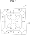
- FIG. 1 is a plan view illustrating an example of a configuration of a quantum operation device 10 according to an embodiment of the disclosed technology.
- the quantum operation device 10 includes a qubit element (qubit) 20, a resonator 21, and a readout electrode 22 provided to a first substrate 30.
- qubit qubit element
- the qubit element 20 is an element that forms a coherent two-level system using superconductivity.
- FIG. 2 is a diagram illustrating an example of a circuit configuration of the qubit element 20.
- the qubit element 20 performs a quantum operation using nonlinear energy, and is configured by including a transmon qubit circuit in which a superconducting Josephson device 201 and a capacitor 202 are coupled in parallel.
- the superconducting Josephson device 201 is configured by including a pair of superconductors that exhibit superconductivity at a temperature equal to or lower than a predetermined critical temperature, and an ultrathin insulator having a thickness of about several nm sandwiched between the pair of superconductors.
- the superconductor may be, for example, aluminum, and the insulator may be, for example, aluminum oxide.
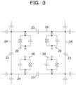
- a plurality of the qubit elements 20 is coupled to other adjacent qubit elements 20 via inter-bit wiring 24.
- Capacitors 23 are provided in a path of the inter-bit wiring 24.
- each of the qubit elements 20 creates a quantum entanglement state with the other adjacent qubit elements 20 and performs a quantum operation.
- the resonator 21 interacts with the qubit element 20 to read out a bit signal indicating a state of the qubit element 20.
- the resonator 21 is coupled to the qubit element 20 via a capacitor (not illustrated).
- FIG. 4 is a diagram illustrating an example of a circuit configuration of the resonator 21.
- the resonator 21 is configured by including a resonance circuit in which a superconducting inductor 211 and a capacitor 212 are coupled in parallel.
- the readout electrode 22 is an electrode that is coupled to the resonator 21 and is for extracting the bit signal read out by the resonator 21 to the outside.
- FIG. 5 is a schematic cross-sectional view illustrating an example of the configuration of the quantum operation device 10. Note that, in FIG. 5 , illustration of the resonator 21 (see FIG. 1 ) is omitted. Furthermore, FIG. 5 illustrates only the configuration around one qubit element 20 extracted.
- the quantum operation device 10 has a configuration in which the first substrate 30, a second substrate 40, and a cover 50 are stacked.
- the qubit element 20 is mounted to a first surface S1 of the first substrate 30.
- An insulating film that causes a dielectric loss is not provided to a surface of the qubit element 20.
- the resonator 21 not illustrated in FIG. 5 may be mounted to the first surface S1 of the first substrate 30.
- Through-vias 31A and 31B are provided in the first substrate 30.
- the through-vias 31A and 31B are configured by including through-holes 32A and 32B penetrating the first substrate 30, and conductive films 33A and 33B covering inner walls of the through-holes 32A and 32B, respectively.
- the conductive films 33A and 33B have portions extending at the first surface S1 and a second surface S2 opposite to the first surface S1 of the first substrate 30.
- the through-via 31A is used to supply a ground potential to the first substrate 30 and the cover 50.
- the through-via 31B functions as the readout electrode 22.
- the second surface S2 of the first substrate 30 is provided with a control electrode 37 to which a qubit control signal for controlling the qubit element 20 is supplied.
- the control electrode 37 is arranged immediately below the qubit element 20 mounted to the first surface S1, and the qubit control signal supplied to the control electrode 37 is transmitted to the qubit element 20 via a base material of the first substrate 30.
- an insulator or a semiconductor may be used, and for example, silicon may be suitably used.
- the conductive films 33A and 33B constituting the through-vias 31A and 31B and the control electrode 37 are preferably configured by a metal that exhibits superconductivity at a temperature equal to or lower than a predetermined temperature.
- a metal for example, niobium (Nb) may be suitably used.
- the cover 50 covers a side of the first surface S1 of the first substrate 30.
- the cover 50 forms a sealed space 51 around the qubit element 20 and the readout electrode 22. Recessed portions for forming the sealed space 51 may be formed in a portion of the cover 50 facing the qubit element 20 and the readout electrode 22.
- the sealed space 51 communicates with the through-holes 32A and 32B.
- the sealed space 51 is preferably a vacuum. By making the sealed space 51 a vacuum, adsorption of a substance to the qubit element 20 may be suppressed without forming a protective film that causes a dielectric loss at the surface of the qubit element 20, and a clean state of the surface of the qubit element 20 may be always kept.
- the vacuum is not limited to a complete vacuum, and includes a low pressure state to such an extent that an effect of substantially suppressing adsorption of a substance to the qubit element 20 is exhibited.
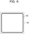
- FIG. 6 is a plan view illustrating an example of a form of a seal member 60 that forms a joint portion between the cover 50 and the first substrate 30.
- the cover 50 is joined to the first substrate 30 via the ring-shaped seal member 60 surrounding an outer periphery of the qubit element 20 and the readout electrode 22.
- the cover 50 is joined to the first substrate 30 via the ring-shaped seal member 60, so that a sealed state in the sealed space 51 is achieved.
- the cover 50 is preferably configured by a conductor, and is preferably configured by a metal that exhibits superconductivity at a temperature equal to or lower than a predetermined temperature.
- a material constituting the cover 50 for example, aluminum (Al) may be suitably used.
- the cover 50 is joined to the through-via 31A to which the ground potential is supplied via a bump 52. As a result, a potential of the cover 50 may be fixed to the ground potential, and noise coming from the outside and noise radiated from the qubit element 20 and the like may be shielded.
- the seal member 60 and the bump 52 are preferably configured by including a metal that exhibits superconductivity at a temperature equal to or lower than a predetermined temperature.
- a metal for example, indium (In) may be suitably used.
- the seal member 60 and the bump 52 are joined to the cover 50 via a conductive film 53 configured by including a metal that exhibits superconductivity at a temperature equal to or lower than a predetermined temperature, such as niobium (Nb).
- a conductive film 53 configured by including a metal that exhibits superconductivity at a temperature equal to or lower than a predetermined temperature, such as niobium (Nb).
- Nb niobium
- the material of the cover 50 it is also possible to use an insulator or a semiconductor having a surface provided with a metal film that exhibits superconductivity.
- the second substrate 40 is provided on a side of the second surface S2 of the first substrate 30.
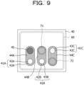
- the second substrate 40 includes through-vias 41A, 41B, and 41C and conductive pads 44A, 44B, and 44C coupled to these through-vias.
- the through-vias 41A, 41B, and 41C are configured by including through-holes 42A, 42B, and 42C penetrating the second substrate 40, and conductive films 43A, 43B, and 43C covering inner walls of these through-holes, respectively.
- the conductive pad 44A is coupled to the control electrode 37 via a bump 45.
- the qubit control signal is input from a back surface of the second substrate 40 (a surface opposite to a joint surface with the first substrate 30), and is supplied to the control electrode 37 via the through-via 41A, the conductive pad 44A, and the bump 45.
- the conductive pad 44B is coupled to the through-via 31A of the first substrate 30 via a seal member 71.
- the ground potential is input from the back surface of the second substrate 40, and is supplied to various elements formed in the first substrate 30 and the cover 50 via the through-via 41B, the conductive pad 44B, the seal member 71, and the through-via 31A.
- the conductive pad 44C is coupled to the through-via 31B (readout electrode 22) of the first substrate 30 via a seal member 72.
- a readout control signal for reading out the bit signal indicating the state of the qubit element 20 is input from the back surface of the second substrate 40 and supplied to the through-via 31B (readout electrode 22) via the through-via 41C, the conductive pad 44C, and the seal member 72.
- the bit signal read out from the qubit element 20 is extracted to the outside along a path opposite to the path of the readout control signal.
- the second substrate 40 is joined to the first substrate 30 via the bump 45 and the seal members 71 and 72.
- FIG. 7 is a plan view illustrating an example of forms of the seal members 71 and 72 and the conductive pads 44B and 44C.
- the seal members 71 and 72 respectively have a ring shape surrounding outer peripheries of open ends on the side of the second surface S2 of the through-holes 32A and 32B constituting the through-vias 31A and 31B of the first substrate 30.
- the through-vias 31A and 31B are respectively joined to the conductive pads 44B and 44C via the seal members 71 and 72, so that the open ends of the through-holes 32A and 32B at the second surfaces S2 are closed.
- the sealed space 51 communicating with the through-holes 32A and 32B is brought into a completely sealed state. In other words, the vacuum state is maintained in the sealed space 51.
- an insulator or a semiconductor may be used, and for example, silicon may be suitably used.
- Each of the seal members 71 and 72, the bump 45, the conductive films 43A, 43B, and 43C, and the conductive pads 44A, 44B, and 44C is preferably configured by including a metal that exhibits superconductivity at a temperature equal to or lower than a predetermined temperature.
- a metal constituting the seal members 71 and 72 and the bump 45 for example, indium (In) may be suitably used.
- niobium (Nb) may be suitably used.
- a material of the second substrate 40 may be an insulator and a semiconductor.
- silicon may be suitably used.
- the seal members 71 and 72 and the bump 45 are preferably configured by a metal that exhibits superconductivity at a temperature equal to or lower than a predetermined temperature.
- a metal for example, indium (In) may be suitably used.
- the conductive films 43A, 43B, and 43C and the conductive pads 44A, 44B, and 44C constituting the through-vias 41A, 41B, and 41C are preferably configured by a metal that exhibits superconductivity at a temperature equal to or lower than a predetermined temperature.
- niobium (Nb) may be suitably used.
- FIG. 8 is a plan view illustrating an example of arrangement of the seal member 60, the through-vias 31A and 31B, the seal members 71 and 72 associated with the through-vias 31A and 31B, the control electrode 37, and the bump 45 associated with the control electrode 37 in the first substrate 30.
- FIG. 9 is a plan view illustrating an example of arrangement of the through-vias 41A, 41B, and 41C, the conductive pads 44A, 44B, and 44C, and the bump 45 in the second substrate 40.
- the first substrate 30 is prepared.
- a silicon substrate may be used.
- a resist (not illustrated) is formed at a surface of the first substrate 30, and this resist is patterned.
- the through-holes 32A and 32B are formed in the first substrate 30 by, for example, deep reactive ion etching (RIE) ( FIG. 10 ).
- RIE deep reactive ion etching
- a predetermined critical temperature such as niobium (Nb)
- Nb niobium
- the conductive film 33 is patterned by photolithography and dry etching. As a result, the through-vias 31A and 31B and the control electrode 37 are formed.
- the through-via 31B functions as the readout electrode 22.
- the qubit element 20 including a superconducting Josephson device is formed at the first surface S1 of the first substrate 30 using Al or the like ( FIG. 12 ).
- the cover 50 is prepared.
- the cover 50 is preferably configured by, for example, a metal that exhibits superconductivity at a temperature equal to or lower than a predetermined critical temperature, such as aluminum (Al).
- the recessed portions may be formed in the portion of the cover 50 facing the qubit element 20 and the readout electrode 22.
- the ring-shaped seal member 60 is formed at the portion of the cover 50 surrounding the outer periphery of the qubit element 20 and the readout electrode 22 via the conductive film 53.
- the bump 52 is formed at a portion of the cover 50 corresponding to the through-via 31A via the conductive film 53.
- the seal member 60 and the bump 52 are preferably configured by a metal that exhibits superconductivity at a temperature equal to or lower than a predetermined critical temperature, such as indium (In).
- the conductive film 53 is preferably configured by a metal that exhibits superconductivity at a temperature equal to or lower than a predetermined critical temperature, such as niobium (Nb) ( FIG. 13 ).
- the cover 50 and the first substrate 30 are housed in a vacuum chamber (not illustrated). Thereafter, oxide at surfaces of the seal member 60 and the bump 52 is removed by a surface treatment such as Ar ion milling in the vacuum chamber.
- the first substrate 30 and the cover 50 are heated in a state of being brought into close contact with each other in the vacuum chamber.
- a heating temperature is determined according to melting points of the seal member 60 and the bump 52. In a case where the seal member 60 and the bump 52 are configured by indium (In), for example, the heating temperature is preferably equal to or higher than 100°C and equal to or lower than 150°C.
- the seal member 60 and the bump 52 are melted, the first substrate 30 and the cover 50 are joined, and the sealed space 51 communicating with the through-holes 32A and 32B is formed around the qubit element 20 and the readout electrode 22.
- the cover 50 is joined to the first substrate 30 via the ring-shaped seal member 60, so that the sealed state in the sealed space 51 is achieved ( FIG. 14 ).
- the second substrate 40 is prepared.
- a silicon substrate may be used.
- the through-vias 41A, 41B, and 41C and the conductive pads 44A, 44B, and 44C are formed in the second substrate 40. Formation procedures of these are similar to the formation procedures of the through-vias 31A and 31B in the first substrate 30.
- the bump 45 is formed at a surface of the conductive pad 44A.
- the seal members 71 and 72 are formed at surfaces of the conductive pads 44B and 44C.
- the seal members 71 and 72 respectively have the ring shape surrounding the outer peripheries of the open ends on the side of the second surface S2 of the through-holes 32A and 32B.
- the seal members 71 and 72 and the bump 45 are preferably configured by a metal that exhibits superconductivity at a temperature equal to or lower than a predetermined critical temperature, such as indium (In) ( FIG. 15 ).
- the stack of the cover 50 and the first substrate 30, and the second substrate 40 are housed in the vacuum chamber. Thereafter, oxide at surfaces of the seal members 71 and 72 and the bump 45 is removed by the surface treatment such as the Ar ion milling. Next, a surface treatment gas such as a vapor HF gas is introduced into the sealed space 51 from the through-holes 32A and 32B in the vacuum chamber to remove oxide or the like at the surface of the qubit element 20. As a result, the surface of the qubit element 20 is cleaned without damaging the qubit element 20.
- a surface treatment gas such as a vapor HF gas
- a heating temperature is determined according to melting points of the seal members 71 and 72 and the bump 45.
- the heating temperature is preferably equal to or higher than 100°C and equal to or lower than 150°C.
- the through-vias 31A and 31B are respectively joined to the conductive pads 44B and 44C via the seal members 71 and 72, so that the open ends of the through-holes 32A and 32B at the second surfaces S2 are closed.
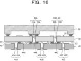
- the sealed space 51 communicating with the through-holes 32A and 32B is brought into the completely sealed state. In other words, the vacuum state is maintained in the sealed space 51 ( FIG. 16 ).
- the quantum operation device 10 includes the first substrate 30 having the first surface S1 mounted with the qubit element 20, the cover 50 covering the side of the first surface S1 of the first substrate 30, and the second substrate 40 provided on the side of the second surface S2 of the first substrate 30.
- the first substrate 30 includes the through-vias 31A and 31B including the through-holes 32A and 32B and the conductive films 33A and 33B.
- the cover 50 forms the sealed space 51 communicating with the through-holes 32A and 32B around the qubit element 20.
- the open ends of the through-holes 32A and 32B at the second surface S2 are closed by the second substrate 40.
- the surface of the qubit element 20 may be kept clean. In other words, adsorption of a substance to the surface of the qubit element 20 may be suppressed, and shortening of a coherence time caused by the adsorbate may be avoided.
- the second substrate 40 is joined to the first substrate 30 via the ring-shaped seal members 71 and 72 surrounding the outer peripheries of the open ends of the through-holes 32A and 32B, and the cover 50 is joined to the first substrate 30 via the ring-shaped seal member 60 surrounding the sealed space 51.
- the sealed space 51 may be brought into the completely sealed state and may be maintained in the vacuum state.
- the second substrate 40 includes the conductive pads 44A, 44B, and 44C electrically coupled to the through-vias 31A and 31B provided in the first substrate 30, and the through-vias 41A, 41B, and 41C electrically coupled to these conductive pads.
- the wiring and the qubit elements 20 may be integrated at a high density, which may contribute to miniaturization of the quantum operation device 10.
- metal Al
- niobium (Nb), and indium (In) are exemplified as the metal that exhibits superconductivity at a temperature equal to or lower than a predetermined critical temperature, but it is also possible to use a metal such as niobium nitride (NbN), tantalum (Ta), tantalum nitride (TaN), or titanium nitride (TiN).
- NbN niobium nitride
- Ta tantalum
- TaN tantalum nitride
- TiN titanium nitride
- FIG. 17 is a schematic cross-sectional view illustrating an example of a configuration of a quantum operation device 10A according to a second embodiment of the disclosed technology. Note that, in FIG. 17 , illustration of a resonator 21 and a readout electrode 22 is omitted. Furthermore, FIG. 17 illustrates only a configuration around one qubit element 20 extracted.
- the quantum operation device 10A has a configuration in which a first substrate 30, a second substrate 40, and a cover 50 are stacked.
- the cover 50 covers a side of a first surface S1 of the first substrate 30 while forming a sealed space 51 around the qubit element 20.
- the second substrate 40 is provided on a side of a second surface S2 of the first substrate 30, and closes open ends on the side of the second surface S2 of the respective through-holes constituting through-vias 31P, 31Q, 31R, and 31S provided in the first substrate 30.
- the first surface S1 of the first substrate 30 is mounted with a plurality of the qubit elements 20.
- the sealed spaces 51 are formed to be separated from each other for each qubit element 20.
- FIG. 18 is a plan view illustrating an example of a form of a seal member 60 that forms a joint portion between the cover 50 and the first substrate 30.
- the cover 50 is joined to the first substrate 30 via the ring-shaped seal members 60 surrounding outer peripheries of the qubit elements 20.
- the cover 50 is joined to the first substrate 30 via the ring-shaped seal members 60, so that sealed states in the sealed spaces 51 are achieved.
- the sealed spaces 51 provided for the respective qubit elements 20 are separated from each other by the seal members 60.
- Each of the plurality of qubit elements 20 mounted to the first surface S1 of the first substrate 30 is coupled to other adjacent qubit elements 20 via inter-bit wiring 24.
- a part of the inter-bit wiring 24 is provided to the first substrate 30, and another part of the inter-bit wiring 24 is provided to the second substrate 40.
- FIG. 18 portions of the inter-bit wiring 24, which are provided to the first substrate 30, are illustrated. As illustrated in FIGs. 17 and 18 , portions of the inter-bit wiring 24 intersecting the seal member 60 are provided to the second substrate 40, and the other portions of the inter-bit wiring 24 are provided to the first surface S1 of the first substrate 30.
- the inter-bit wiring 24 bypasses to the second substrate 40 at the portions intersecting the seal member 60.
- the portions of the inter-bit wiring 24 provided to the first substrate 30 (hereinafter, referred to as first portions) and the portions provided to the second substrate 40 (second portions) are coupled to each other via the through-vias 31P, 31Q, 31R, and 31S.
- Broken-line arrows illustrated in FIG. 17 indicate paths of bit signals from the qubit element 20 to other adjacent qubit elements (not illustrated).
- the bit signal output from the qubit element 20 is transmitted to another adjacent qubit element (not illustrated) through the first portion of the inter-bit wiring 24, the through-via 31P, the second portion of the inter-bit wiring 24, the through-via 31Q, and the first portion of the inter-bit wiring 24.
- the sealed spaces 51 are formed to be separated from each other for the respective qubit elements 20.
- the other sealed spaces 51 may be maintained in the vacuum state.
- an influence in the case where the vacuum is broken may be reduced.
- the seal members 60 surrounding the outer peripheries of the respective plurality of qubit elements 20 are provided, it is needed to arrange the inter-bit wiring 24 so as not to come into contact with the seal members 60.
- the quantum operation device 10A according to the present embodiment since the portions of the inter-bit wiring 24 intersecting the seal members 60 bypass to the second substrate 40, contact between the inter-bit wiring 24 and the seal members 60 is avoided.
- FIG. 19 is a schematic cross-sectional view illustrating an example of a configuration of a quantum operation device 10B according to a third embodiment of the disclosed technology. Note that, in FIG. 19 , illustration of a resonator 21 and a readout electrode 22 is omitted. Furthermore, FIG. 19 illustrates only a configuration around one qubit element 20 extracted.
- FIG. 20 is a plan view illustrating an example of a form of a seal member 60 that forms a joint portion between a cover 50 and a first substrate 30.
- the quantum operation device 10B according to the present embodiment is different from the quantum operation device 10A according to the second embodiment described above in that all portions of inter-bit wiring 24 are provided to the first substrate 30.
- insulators 80 that separate the seal member 60 and the inter-bit wiring 24 are provided at intersection portions between the seal member 60 and the inter-bit wiring 24. In other words, by sandwiching the insulators 80 between the seal member 60 and the inter-bit wiring 24, contact between the seal member 60 and the inter-bit wiring 24 is avoided. According to the quantum operation device 10B according to the present embodiment, through-vias for causing the inter-bit wiring 24 to bypass to the second substrate 40 become unnecessary.
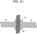
- FIG. 21 is a plan view illustrating an example of a pattern of a capacitor 23 provided in a path of the inter-bit wiring 24.
- the capacitor 23 may have a comb-shaped pattern.
- the insulator 80 provided at the intersection portion between the seal member 60 and the inter-bit wiring 24 may be provided at a position overlapping the capacitor 23.
- parasitic capacitance by the insulator 80 may be taken into the capacitor 23, and designing may be facilitated.
- a configuration may be adopted in which the capacitor 23 is arranged outside a region surrounded by the seal member 60 so that one capacitor 23 is provided for two qubit elements 20 adjacent to each other.
- FIG. 22 is a schematic cross-sectional view illustrating an example of a configuration of a quantum operation device 10C according to a fourth embodiment of the disclosed technology.
- the quantum operation device 10C according to the fourth embodiment has a configuration in which structures 90A and 90B each including a cover 50, a first substrate 30, and a second substrate 40 are stacked.
- the structures 90A and 90B each have a configuration similar to that of the quantum operation device 10 according to the first embodiment described above.
- the structures 90A and 90B are stacked by joining the respective covers 50 to each other.
- the respective second substrates 40 are arranged in an uppermost layer and a lowermost layer of the quantum operation device 10C.
- qubit elements 20 may be integrated at a high density. Furthermore, since the second substrates 40 are arranged in the uppermost layer and the lowermost layer, wiring for accessing the qubit elements 20 may be extracted in two directions, and access to the qubit elements 20 from the two directions may be performed.
Landscapes
- Engineering & Computer Science (AREA)
- Manufacturing & Machinery (AREA)
- General Physics & Mathematics (AREA)
- Microelectronics & Electronic Packaging (AREA)
- Physics & Mathematics (AREA)
- Theoretical Computer Science (AREA)
- Mathematical Analysis (AREA)
- Computing Systems (AREA)
- Evolutionary Computation (AREA)
- Condensed Matter Physics & Semiconductors (AREA)
- Computational Mathematics (AREA)
- Mathematical Optimization (AREA)
- Pure & Applied Mathematics (AREA)
- Data Mining & Analysis (AREA)
- General Engineering & Computer Science (AREA)
- Mathematical Physics (AREA)
- Software Systems (AREA)
- Artificial Intelligence (AREA)
- Internal Circuitry In Semiconductor Integrated Circuit Devices (AREA)
- Superconductor Devices And Manufacturing Methods Thereof (AREA)
- Semiconductor Memories (AREA)
Abstract
Description
- The disclosed technology relates to a quantum operation device and a method of manufacturing the quantum operation device.
- The following technology is known as a technology related to a quantum operation device. For example, a technology is known in which a cap layer is bonded to a substrate at which a qubit element is formed to form a sealed vacuum cavity between the cap layer and the substrate.
- Furthermore, a technology is known in which, in a stacked quantum computing device, a first chip includes superconducting qubits and is bonded to a second chip that contains one or a plurality of wiring layers, as well as qubit control and qubit readout elements, integrated with lossy dielectrics.
- As a qubit element (qubit) constituting the quantum operation device, one using a transmon is known. The transmon has a configuration in which a superconducting Josephson device and a capacitor are coupled in parallel, and performs a quantum operation using nonlinear energy. The transmon operates with extremely small energy, and is thus easily affected by external noise. A time during which the quantum operation may be sustained in the transmon is referred to as a coherence time. The coherence time is sensitively affected by a state around the transmon. For example, in a case where there is a dielectric such as an oxide film around the transmon, the coherence time is shortened due to a dielectric loss. Therefore, it is common that an insulating film such as a protective film is not formed at a surface of the transmon. The quantum operation device configured by including the qubit element is kept at a very low temperature in a vacuum chamber, but an adsorbate that is adsorbed in the atmosphere and causes decoherence is cooled and remains as it is. Since the coherence time is shortened by the adsorbate adsorbed to a surface of the qubit element, it is needed to always keep a clean state of the surface of the qubit element.
- An object of the disclosed technology is to keep a surface of a qubit element clean in a quantum operation device.
- A quantum operation device according to the disclosed technology includes: a first substrate that has a through-hole; a qubit element formed at a first surface of the substrate; a cover that covers a side of the first surface of the first substrate; and a second substrate that is provided on a side of a second surface opposite to the side of the first surface of the first substrate and that closes an open end of the through-hole on the side of the second surface. A sealed space that surrounds the qubit element and communicates with the through-hole is provided between the first surface and the cover.
- According to the disclosed technology, it is possible to keep a surface of a qubit element clean in a quantum operation device.
-
-
FIG. 1 is a plan view illustrating an example of a configuration of a quantum operation device according to an embodiment of the disclosed technology. -
FIG. 2 is a diagram illustrating an example of a circuit configuration of a qubit element according to the embodiment of the disclosed technology. -
FIG. 3 is a diagram illustrating an example of a coupling configuration between qubit elements according to the embodiment of the disclosed technology. -
FIG. 4 is a diagram illustrating an example of a circuit configuration of a resonator according to the embodiment of the disclosed technology. -
FIG. 5 is a schematic cross-sectional view illustrating an example of the configuration of the quantum operation device according to the embodiment of the disclosed technology. -
FIG. 6 is a plan view illustrating an example of a form of a seal member that forms a joint portion between a cover and a first substrate according to the embodiment of the disclosed technology. -
FIG. 7 is a plan view illustrating an example of forms of seal members and conductive pads according to the embodiment of the disclosed technology. -
FIG. 8 is a plan view illustrating an example of arrangement of through-vias, the seal members, a control electrode, and a bump in the first substrate according to the embodiment of the disclosed technology. -
FIG. 9 is a plan view illustrating an example of arrangement of through-vias, conductive pads, and the bump in a second substrate according to the embodiment of the disclosed technology. -
FIG. 10 is a cross-sectional view illustrating an example of a method of manufacturing the quantum operation device according to the embodiment of the disclosed technology. -
FIG. 11 is a cross-sectional view illustrating the example of the method of manufacturing the quantum operation device according to the embodiment of the disclosed technology. -
FIG. 12 is a cross-sectional view illustrating the example of the method of manufacturing the quantum operation device according to the embodiment of the disclosed technology. -
FIG. 13 is a cross-sectional view illustrating the example of the method of manufacturing the quantum operation device according to the embodiment of the disclosed technology. -
FIG. 14 is a cross-sectional view illustrating the example of the method of manufacturing the quantum operation device according to the embodiment of the disclosed technology. -
FIG. 15 is a cross-sectional view illustrating the example of the method of manufacturing the quantum operation device according to the embodiment of the disclosed technology. -
FIG. 16 is a cross-sectional view illustrating the example of the method of manufacturing the quantum operation device according to the embodiment of the disclosed technology. -
FIG. 17 is a schematic cross-sectional view illustrating an example of a configuration of a quantum operation device according to an embodiment of the disclosed technology. -
FIG. 18 is a plan view illustrating an example of a form of a seal member that forms a joint portion between a cover and a first substrate according to the embodiment of the disclosed technology. -
FIG. 19 is a schematic cross-sectional view illustrating an example of a configuration of a quantum operation device according to an embodiment of the disclosed technology. -
FIG. 20 is a plan view illustrating an example of a form of a seal member that forms a joint portion between a cover and a first substrate according to the embodiment of the disclosed technology. -
FIG. 21 is a plan view illustrating an example of a pattern of a capacitor provided in a path of inter-bit wiring according to the embodiment of the disclosed technology. -
FIG. 22 is a schematic cross-sectional view illustrating an example of a configuration of a quantum operation device according to an embodiment of the disclosed technology. - Hereinafter, an example of embodiments of the disclosed technology will be described with reference to the drawings. Note that, in each drawing, the same or equivalent components and portions are denoted with the same reference signs, and redundant description will be omitted.
-
FIG. 1 is a plan view illustrating an example of a configuration of aquantum operation device 10 according to an embodiment of the disclosed technology. Thequantum operation device 10 includes a qubit element (qubit) 20, aresonator 21, and areadout electrode 22 provided to afirst substrate 30. - The
qubit element 20 is an element that forms a coherent two-level system using superconductivity.FIG. 2 is a diagram illustrating an example of a circuit configuration of thequbit element 20. Thequbit element 20 performs a quantum operation using nonlinear energy, and is configured by including a transmon qubit circuit in which a superconducting Josephsondevice 201 and acapacitor 202 are coupled in parallel. The superconducting Josephsondevice 201 is configured by including a pair of superconductors that exhibit superconductivity at a temperature equal to or lower than a predetermined critical temperature, and an ultrathin insulator having a thickness of about several nm sandwiched between the pair of superconductors. The superconductor may be, for example, aluminum, and the insulator may be, for example, aluminum oxide. As illustrated inFIG. 3 , in thequantum operation device 10, a plurality of thequbit elements 20 is coupled to otheradjacent qubit elements 20 viainter-bit wiring 24.Capacitors 23 are provided in a path of theinter-bit wiring 24. As a result, each of thequbit elements 20 creates a quantum entanglement state with the otheradjacent qubit elements 20 and performs a quantum operation. - The
resonator 21 interacts with thequbit element 20 to read out a bit signal indicating a state of thequbit element 20. Theresonator 21 is coupled to thequbit element 20 via a capacitor (not illustrated).FIG. 4 is a diagram illustrating an example of a circuit configuration of theresonator 21. Theresonator 21 is configured by including a resonance circuit in which asuperconducting inductor 211 and acapacitor 212 are coupled in parallel. Thereadout electrode 22 is an electrode that is coupled to theresonator 21 and is for extracting the bit signal read out by theresonator 21 to the outside. -
FIG. 5 is a schematic cross-sectional view illustrating an example of the configuration of thequantum operation device 10. Note that, inFIG. 5 , illustration of the resonator 21 (seeFIG. 1 ) is omitted. Furthermore,FIG. 5 illustrates only the configuration around onequbit element 20 extracted. Thequantum operation device 10 has a configuration in which thefirst substrate 30, asecond substrate 40, and acover 50 are stacked. - The
qubit element 20 is mounted to a first surface S1 of thefirst substrate 30. An insulating film that causes a dielectric loss is not provided to a surface of thequbit element 20. Theresonator 21 not illustrated inFIG. 5 may be mounted to the first surface S1 of thefirst substrate 30. Through-vias first substrate 30. The through-vias holes first substrate 30, andconductive films holes conductive films first substrate 30. - The through-via 31A is used to supply a ground potential to the
first substrate 30 and thecover 50. The through-via 31B functions as thereadout electrode 22. The second surface S2 of thefirst substrate 30 is provided with acontrol electrode 37 to which a qubit control signal for controlling thequbit element 20 is supplied. Thecontrol electrode 37 is arranged immediately below thequbit element 20 mounted to the first surface S1, and the qubit control signal supplied to thecontrol electrode 37 is transmitted to thequbit element 20 via a base material of thefirst substrate 30. - As the base material of the
first substrate 30, an insulator or a semiconductor may be used, and for example, silicon may be suitably used. Theconductive films vias control electrode 37 are preferably configured by a metal that exhibits superconductivity at a temperature equal to or lower than a predetermined temperature. As such a metal, for example, niobium (Nb) may be suitably used. - The
cover 50 covers a side of the first surface S1 of thefirst substrate 30. Thecover 50 forms a sealedspace 51 around thequbit element 20 and thereadout electrode 22. Recessed portions for forming the sealedspace 51 may be formed in a portion of thecover 50 facing thequbit element 20 and thereadout electrode 22. The sealedspace 51 communicates with the through-holes space 51 is preferably a vacuum. By making the sealed space 51 a vacuum, adsorption of a substance to thequbit element 20 may be suppressed without forming a protective film that causes a dielectric loss at the surface of thequbit element 20, and a clean state of the surface of thequbit element 20 may be always kept. Note that the vacuum is not limited to a complete vacuum, and includes a low pressure state to such an extent that an effect of substantially suppressing adsorption of a substance to thequbit element 20 is exhibited. -
FIG. 6 is a plan view illustrating an example of a form of aseal member 60 that forms a joint portion between thecover 50 and thefirst substrate 30. Thecover 50 is joined to thefirst substrate 30 via the ring-shapedseal member 60 surrounding an outer periphery of thequbit element 20 and thereadout electrode 22. Thecover 50 is joined to thefirst substrate 30 via the ring-shapedseal member 60, so that a sealed state in the sealedspace 51 is achieved. - The
cover 50 is preferably configured by a conductor, and is preferably configured by a metal that exhibits superconductivity at a temperature equal to or lower than a predetermined temperature. As a material constituting thecover 50, for example, aluminum (Al) may be suitably used. Thecover 50 is joined to the through-via 31A to which the ground potential is supplied via abump 52. As a result, a potential of thecover 50 may be fixed to the ground potential, and noise coming from the outside and noise radiated from thequbit element 20 and the like may be shielded. Theseal member 60 and thebump 52 are preferably configured by including a metal that exhibits superconductivity at a temperature equal to or lower than a predetermined temperature. As such a metal, for example, indium (In) may be suitably used. Theseal member 60 and thebump 52 are joined to thecover 50 via aconductive film 53 configured by including a metal that exhibits superconductivity at a temperature equal to or lower than a predetermined temperature, such as niobium (Nb). Note that, as the material of thecover 50, it is also possible to use an insulator or a semiconductor having a surface provided with a metal film that exhibits superconductivity. - The
second substrate 40 is provided on a side of the second surface S2 of thefirst substrate 30. Thesecond substrate 40 includes through-vias conductive pads vias holes second substrate 40, andconductive films - The
conductive pad 44A is coupled to thecontrol electrode 37 via abump 45. The qubit control signal is input from a back surface of the second substrate 40 (a surface opposite to a joint surface with the first substrate 30), and is supplied to thecontrol electrode 37 via the through-via 41A, theconductive pad 44A, and thebump 45. - The
conductive pad 44B is coupled to the through-via 31A of thefirst substrate 30 via aseal member 71. The ground potential is input from the back surface of thesecond substrate 40, and is supplied to various elements formed in thefirst substrate 30 and thecover 50 via the through-via 41B, theconductive pad 44B, theseal member 71, and the through-via 31A. - The
conductive pad 44C is coupled to the through-via 31B (readout electrode 22) of thefirst substrate 30 via aseal member 72. A readout control signal for reading out the bit signal indicating the state of thequbit element 20 is input from the back surface of thesecond substrate 40 and supplied to the through-via 31B (readout electrode 22) via the through-via 41C, theconductive pad 44C, and theseal member 72. The bit signal read out from thequbit element 20 is extracted to the outside along a path opposite to the path of the readout control signal. Thesecond substrate 40 is joined to thefirst substrate 30 via thebump 45 and theseal members -
FIG. 7 is a plan view illustrating an example of forms of theseal members conductive pads seal members holes vias first substrate 30. The through-vias conductive pads seal members holes space 51 communicating with the through-holes space 51. - As a base material of the
second substrate 40, an insulator or a semiconductor may be used, and for example, silicon may be suitably used. Each of theseal members bump 45, theconductive films conductive pads seal members bump 45, for example, indium (In) may be suitably used. As a metal constituting theconductive films conductive pads - A material of the
second substrate 40 may be an insulator and a semiconductor. As the material of thesecond substrate 40, for example, silicon may be suitably used. Theseal members bump 45 are preferably configured by a metal that exhibits superconductivity at a temperature equal to or lower than a predetermined temperature. As such a metal, for example, indium (In) may be suitably used. Theconductive films conductive pads vias -
FIG. 8 is a plan view illustrating an example of arrangement of theseal member 60, the through-vias seal members vias control electrode 37, and thebump 45 associated with thecontrol electrode 37 in thefirst substrate 30.FIG. 9 is a plan view illustrating an example of arrangement of the through-vias conductive pads bump 45 in thesecond substrate 40. - Hereinafter, an example of a method of manufacturing the
quantum operation device 10 will be described with reference toFIGs. 10 to 16 . First, thefirst substrate 30 is prepared. As thefirst substrate 30, for example, a silicon substrate may be used. Next, a resist (not illustrated) is formed at a surface of thefirst substrate 30, and this resist is patterned. Using the patterned resist as a mask, the through-holes first substrate 30 by, for example, deep reactive ion etching (RIE) (FIG. 10 ). - Next, a
conductive film 33 including a metal that exhibits superconductivity at a temperature equal to or lower than a predetermined critical temperature, such as niobium (Nb), is formed at the first surface S1 and the second surface S2 of thefirst substrate 30 by a sputtering method. The inner walls of the through-holes FIG. 11 ). - Next, the
conductive film 33 is patterned by photolithography and dry etching. As a result, the through-vias control electrode 37 are formed. The through-via 31B functions as thereadout electrode 22. Furthermore, thequbit element 20 including a superconducting Josephson device is formed at the first surface S1 of thefirst substrate 30 using Al or the like (FIG. 12 ). - Next, the
cover 50 is prepared. Thecover 50 is preferably configured by, for example, a metal that exhibits superconductivity at a temperature equal to or lower than a predetermined critical temperature, such as aluminum (Al). The recessed portions may be formed in the portion of thecover 50 facing thequbit element 20 and thereadout electrode 22. The ring-shapedseal member 60 is formed at the portion of thecover 50 surrounding the outer periphery of thequbit element 20 and thereadout electrode 22 via theconductive film 53. Furthermore, thebump 52 is formed at a portion of thecover 50 corresponding to the through-via 31A via theconductive film 53. Theseal member 60 and thebump 52 are preferably configured by a metal that exhibits superconductivity at a temperature equal to or lower than a predetermined critical temperature, such as indium (In). Theconductive film 53 is preferably configured by a metal that exhibits superconductivity at a temperature equal to or lower than a predetermined critical temperature, such as niobium (Nb) (FIG. 13 ). - Next, the
cover 50 and thefirst substrate 30 are housed in a vacuum chamber (not illustrated). Thereafter, oxide at surfaces of theseal member 60 and thebump 52 is removed by a surface treatment such as Ar ion milling in the vacuum chamber. Next, thefirst substrate 30 and thecover 50 are heated in a state of being brought into close contact with each other in the vacuum chamber. A heating temperature is determined according to melting points of theseal member 60 and thebump 52. In a case where theseal member 60 and thebump 52 are configured by indium (In), for example, the heating temperature is preferably equal to or higher than 100°C and equal to or lower than 150°C. As a result, theseal member 60 and thebump 52 are melted, thefirst substrate 30 and thecover 50 are joined, and the sealedspace 51 communicating with the through-holes qubit element 20 and thereadout electrode 22. Thecover 50 is joined to thefirst substrate 30 via the ring-shapedseal member 60, so that the sealed state in the sealedspace 51 is achieved (FIG. 14 ). - Next, the
second substrate 40 is prepared. As thesecond substrate 40, for example, a silicon substrate may be used. Next, the through-vias conductive pads second substrate 40. Formation procedures of these are similar to the formation procedures of the through-vias first substrate 30. Next, thebump 45 is formed at a surface of theconductive pad 44A. Moreover, theseal members conductive pads seal members holes seal members bump 45 are preferably configured by a metal that exhibits superconductivity at a temperature equal to or lower than a predetermined critical temperature, such as indium (In) (FIG. 15 ). - Next, the stack of the
cover 50 and thefirst substrate 30, and thesecond substrate 40 are housed in the vacuum chamber. Thereafter, oxide at surfaces of theseal members bump 45 is removed by the surface treatment such as the Ar ion milling. Next, a surface treatment gas such as a vapor HF gas is introduced into the sealedspace 51 from the through-holes qubit element 20. As a result, the surface of thequbit element 20 is cleaned without damaging thequbit element 20. - Next, the
first substrate 30 and thesecond substrate 40 are heated in a state of being brought into close contact with each other in the vacuum chamber. A heating temperature is determined according to melting points of theseal members bump 45. In a case where theseal members bump 45 are configured by indium (In), for example, the heating temperature is preferably equal to or higher than 100°C and equal to or lower than 150°C. As a result, theseal members bump 45 are melted, and thefirst substrate 30 and thesecond substrate 40 are joined. The through-vias conductive pads seal members holes space 51 communicating with the through-holes FIG. 16 ). - As described above, the
quantum operation device 10 includes thefirst substrate 30 having the first surface S1 mounted with thequbit element 20, thecover 50 covering the side of the first surface S1 of thefirst substrate 30, and thesecond substrate 40 provided on the side of the second surface S2 of thefirst substrate 30. Thefirst substrate 30 includes the through-vias holes conductive films cover 50 forms the sealedspace 51 communicating with the through-holes qubit element 20. The open ends of the through-holes second substrate 40. According to thequantum operation device 10 according to the disclosed technology, since the sealed state of the sealedspace 51 is kept, the surface of thequbit element 20 may be kept clean. In other words, adsorption of a substance to the surface of thequbit element 20 may be suppressed, and shortening of a coherence time caused by the adsorbate may be avoided. - Furthermore, the
second substrate 40 is joined to thefirst substrate 30 via the ring-shapedseal members holes cover 50 is joined to thefirst substrate 30 via the ring-shapedseal member 60 surrounding the sealedspace 51. As a result, the sealedspace 51 may be brought into the completely sealed state and may be maintained in the vacuum state. As a result, it is possible to almost completely prevent adsorption of a substance to the surface of thequbit element 20. - The
second substrate 40 includes theconductive pads vias first substrate 30, and the through-vias second substrate 40 as a rewiring layer in this manner, the wiring and thequbit elements 20 may be integrated at a high density, which may contribute to miniaturization of thequantum operation device 10. - Note that, in the embodiment described above, aluminum (Al), niobium (Nb), and indium (In) are exemplified as the metal that exhibits superconductivity at a temperature equal to or lower than a predetermined critical temperature, but it is also possible to use a metal such as niobium nitride (NbN), tantalum (Ta), tantalum nitride (TaN), or titanium nitride (TiN).
-
FIG. 17 is a schematic cross-sectional view illustrating an example of a configuration of aquantum operation device 10A according to a second embodiment of the disclosed technology. Note that, inFIG. 17 , illustration of aresonator 21 and areadout electrode 22 is omitted. Furthermore,FIG. 17 illustrates only a configuration around onequbit element 20 extracted. - Similarly to the
quantum operation device 10 according to the first embodiment, thequantum operation device 10A has a configuration in which afirst substrate 30, asecond substrate 40, and acover 50 are stacked. Thecover 50 covers a side of a first surface S1 of thefirst substrate 30 while forming a sealedspace 51 around thequbit element 20. Thesecond substrate 40 is provided on a side of a second surface S2 of thefirst substrate 30, and closes open ends on the side of the second surface S2 of the respective through-holes constituting through-vias 31P, 31Q, 31R, and 31S provided in thefirst substrate 30. Although not illustrated inFIG. 17 , the first surface S1 of thefirst substrate 30 is mounted with a plurality of thequbit elements 20. The sealedspaces 51 are formed to be separated from each other for eachqubit element 20. -
FIG. 18 is a plan view illustrating an example of a form of aseal member 60 that forms a joint portion between thecover 50 and thefirst substrate 30. For therespective qubit elements 20, thecover 50 is joined to thefirst substrate 30 via the ring-shapedseal members 60 surrounding outer peripheries of thequbit elements 20. Thecover 50 is joined to thefirst substrate 30 via the ring-shapedseal members 60, so that sealed states in the sealedspaces 51 are achieved. The sealedspaces 51 provided for therespective qubit elements 20 are separated from each other by theseal members 60. - Each of the plurality of
qubit elements 20 mounted to the first surface S1 of thefirst substrate 30 is coupled to otheradjacent qubit elements 20 viainter-bit wiring 24. In thequantum operation device 10A according to the present embodiment, a part of theinter-bit wiring 24 is provided to thefirst substrate 30, and another part of theinter-bit wiring 24 is provided to thesecond substrate 40. InFIG. 18 , portions of theinter-bit wiring 24, which are provided to thefirst substrate 30, are illustrated. As illustrated inFIGs. 17 and18 , portions of theinter-bit wiring 24 intersecting theseal member 60 are provided to thesecond substrate 40, and the other portions of theinter-bit wiring 24 are provided to the first surface S1 of thefirst substrate 30. In other words, theinter-bit wiring 24 bypasses to thesecond substrate 40 at the portions intersecting theseal member 60. The portions of theinter-bit wiring 24 provided to the first substrate 30 (hereinafter, referred to as first portions) and the portions provided to the second substrate 40 (second portions) are coupled to each other via the through-vias 31P, 31Q, 31R, and 31S. - Broken-line arrows illustrated in
FIG. 17 indicate paths of bit signals from thequbit element 20 to other adjacent qubit elements (not illustrated). For example, the bit signal output from thequbit element 20 is transmitted to another adjacent qubit element (not illustrated) through the first portion of theinter-bit wiring 24, the through-via 31P, the second portion of theinter-bit wiring 24, the through-via 31Q, and the first portion of theinter-bit wiring 24. - According to the
quantum operation device 10A of the present embodiment, the sealedspaces 51 are formed to be separated from each other for therespective qubit elements 20. As a result, even in a case where the vacuum state may not be maintained in one of the sealedspaces 51, the other sealedspaces 51 may be maintained in the vacuum state. In other words, as compared with a case where the plurality ofqubit elements 20 is integrally vacuum-sealed, an influence in the case where the vacuum is broken may be reduced. - On the other hand, in a case where the
seal members 60 surrounding the outer peripheries of the respective plurality ofqubit elements 20 are provided, it is needed to arrange theinter-bit wiring 24 so as not to come into contact with theseal members 60. According to thequantum operation device 10A according to the present embodiment, since the portions of theinter-bit wiring 24 intersecting theseal members 60 bypass to thesecond substrate 40, contact between theinter-bit wiring 24 and theseal members 60 is avoided. -
FIG. 19 is a schematic cross-sectional view illustrating an example of a configuration of aquantum operation device 10B according to a third embodiment of the disclosed technology. Note that, inFIG. 19 , illustration of aresonator 21 and areadout electrode 22 is omitted. Furthermore,FIG. 19 illustrates only a configuration around onequbit element 20 extracted.FIG. 20 is a plan view illustrating an example of a form of aseal member 60 that forms a joint portion between acover 50 and afirst substrate 30. Thequantum operation device 10B according to the present embodiment is different from thequantum operation device 10A according to the second embodiment described above in that all portions ofinter-bit wiring 24 are provided to thefirst substrate 30. In thequantum operation device 10B according to the present embodiment,insulators 80 that separate theseal member 60 and theinter-bit wiring 24 are provided at intersection portions between theseal member 60 and theinter-bit wiring 24. In other words, by sandwiching theinsulators 80 between theseal member 60 and theinter-bit wiring 24, contact between theseal member 60 and theinter-bit wiring 24 is avoided. According to thequantum operation device 10B according to the present embodiment, through-vias for causing theinter-bit wiring 24 to bypass to thesecond substrate 40 become unnecessary. -
FIG. 21 is a plan view illustrating an example of a pattern of acapacitor 23 provided in a path of theinter-bit wiring 24. As exemplified inFIG. 21 , thecapacitor 23 may have a comb-shaped pattern. Theinsulator 80 provided at the intersection portion between theseal member 60 and theinter-bit wiring 24 may be provided at a position overlapping thecapacitor 23. As a result, parasitic capacitance by theinsulator 80 may be taken into thecapacitor 23, and designing may be facilitated. Note that a configuration may be adopted in which thecapacitor 23 is arranged outside a region surrounded by theseal member 60 so that onecapacitor 23 is provided for twoqubit elements 20 adjacent to each other. -
FIG. 22 is a schematic cross-sectional view illustrating an example of a configuration of aquantum operation device 10C according to a fourth embodiment of the disclosed technology. Thequantum operation device 10C according to the fourth embodiment has a configuration in whichstructures cover 50, afirst substrate 30, and asecond substrate 40 are stacked. Thestructures quantum operation device 10 according to the first embodiment described above. Thestructures second substrates 40 are arranged in an uppermost layer and a lowermost layer of thequantum operation device 10C. - According to the
quantum operation device 10C according to the present embodiment,qubit elements 20 may be integrated at a high density. Furthermore, since thesecond substrates 40 are arranged in the uppermost layer and the lowermost layer, wiring for accessing thequbit elements 20 may be extracted in two directions, and access to thequbit elements 20 from the two directions may be performed. -
- Patent Document 1:
Japanese National Publication of International Patent Application No. 2019-532520 - Patent Document 2:
Japanese National Publication of International Patent Application No. 2020-511794 -
- 10, 10A, 10B, 10C Quantum operation device
- 20 Qubit element
- 23 Capacitor
- 24 Inter-bit wiring
- 30 First substrate
- 31A, 31B, 31C, 31P, 31Q, 31R Through-via
- 32A, 32BThrough-hole
- 33A, 33BConductive film
- 41A, 41B, 41C Through-via
- 44A, 44B, 44C Conductive pad
- 50 Cover
- 60, 71, 72 Seal member
- 80 Insulator
- 90A, 90BStructure
Claims (20)
- A quantum operation device comprising:a first substrate that has a through-hole;a qubit element formed at a first surface of the substrate;a cover that covers a side of the first surface of the first substrate; anda second substrate that is provided on a side of a second surface opposite to the side of the first surface of the first substrate and that closes an open end of the through-hole on the side of the second surface, whereina sealed space that surrounds the qubit element and communicates with the through-hole is provided between the first surface and the cover.
- The quantum operation device according to claim 1, wherein
the second substrate is joined to the second surface of the first substrate via a ring-shaped seal member that surrounds an outer periphery of the open end. - The quantum operation device according to claim 1 or 2, wherein
the cover is joined to the first surface of the first substrate via a ring-shaped seal member that surrounds the sealed space. - The quantum operation device according to any one of claims 1 to 3, wherein
the sealed space is a vacuum. - The quantum operation device according to any one of claims 1 to 4, whereinthe first substrate includes a through-via that includes the through-hole and a conductive film that covers an inner wall of the through-hole, andthe second substrate includes a conductive pad electrically coupled to the through-via and a through-via electrically coupled to the conductive pad.
- The quantum operation device according to any one of claims 1 to 5, whereina plurality of the qubit elements is formed at the first surface of the first substrate, andthe sealed spaces are formed to be separated from each other for the respective plurality of qubit elements.
- The quantum operation device according to claim 6, wherein
at least a part of inter-bit wiring that couples a pair of adjacent qubit elements to each other is provided to the second substrate. - The quantum operation device according to claim 7, whereinthe cover is joined to the first surface of the first substrate via a ring-shaped seal member that surrounds each of the sealed spaces, anda portion of the inter-bit wiring that intersects the ring-shaped seal member that surrounds each of the sealed spaces is provided to the second substrate.
- The quantum operation device according to claim 6, whereininter-bit wiring that couples a pair of adjacent qubit elements to each other is provided to the first surface of the first substrate,the cover is joined to the first surface of the first substrate via a ring-shaped seal member that surrounds each of the sealed spaces, andan insulator that separates the seal member and the inter-bit wiring is provided at an intersection portion between the seal member and the inter-bit wiring.
- The quantum operation device according to claim 9, further comprisinga capacitor provided in a path of the inter-bit wiring, whereinthe intersection portion and the insulator are provided at positions that overlap with the capacitor.
- The quantum operation device according to any one of claims 1 to 10, wherein
a plurality of structures each of which includes the cover, the first substrate, and the second substrate is stacked. - The quantum operation device according to claim 2, wherein
the ring-shaped seal member that surrounds the outer periphery of the open end is configured by including a metal that exhibits superconductivity. - The quantum operation device according to claim 5, wherein
the conductive film and the conductive pad are configured by including a metal that exhibits superconductivity. - A method of manufacturing a quantum operation device, comprising:forming a through-hole in a first substrate;forming a qubit element at a first surface of the first substrate;joining a cover that covers a side of the first surface of the first substrate to the first surface of the first substrate; andjoining, to a second surface opposite to the first surface of the first substrate, a second substrate that closes an open end of the through-hole on a side of the second surface, wherein,in the joining of the cover to the first surface, a sealed space that surrounds the qubit element and communicates with the through-hole is formed between the first surface and the cover.
- The method of manufacturing according to claim 14, wherein
the second substrate is joined to the second surface of the first substrate via a ring-shaped seal member that surrounds an outer periphery of the open end. - The method of manufacturing according to claim 14 or 15, wherein
the cover is joined to the first surface of the first substrate via a ring-shaped seal member that surrounds the sealed space. - The method of manufacturing according to any one of claims 14 to 16, wherein
the joining of the cover to the first substrate and the joining of the second substrate to the first substrate are performed in a vacuum. - The method of manufacturing according to any one of claims 14 to 17, further comprising
cleaning a surface of the qubit element by introducing a gas from the open end of the through-hole, after the joining of the cover to the first substrate and before the joining of the second substrate to the first substrate. - The method of manufacturing according to claim 16, further comprising
removing oxide at a surface of the ring-shaped seal member that surrounds the sealed space, before the joining of the cover to the first substrate. - The method of manufacturing according to claim 15, further comprising
removing oxide at a surface of the ring-shaped seal member that surrounds the outer periphery of the open end, before the joining of the second substrate to the first substrate.
Applications Claiming Priority (1)
| Application Number | Priority Date | Filing Date | Title |
|---|---|---|---|
| PCT/JP2022/000384 WO2023132063A1 (en) | 2022-01-07 | 2022-01-07 | Quantum computing device and method for manufacturing quantum computing device |
Publications (3)
| Publication Number | Publication Date |
|---|---|
| EP4475176A1 true EP4475176A1 (en) | 2024-12-11 |
| EP4475176A4 EP4475176A4 (en) | 2025-10-29 |
| EP4475176B1 EP4475176B1 (en) | 2026-04-29 |
Family
ID=87073584
Family Applications (1)
| Application Number | Title | Priority Date | Filing Date |
|---|---|---|---|
| EP22918652.3A Active EP4475176B1 (en) | 2022-01-07 | 2022-01-07 | Quantum computing device and method for manufacturing quantum computing device |
Country Status (4)
| Country | Link |
|---|---|
| US (1) | US20260082822A1 (en) |
| EP (1) | EP4475176B1 (en) |
| JP (1) | JP7666652B2 (en) |
| WO (1) | WO2023132063A1 (en) |
Families Citing this family (2)
| Publication number | Priority date | Publication date | Assignee | Title |
|---|---|---|---|---|
| JPWO2025046715A1 (en) * | 2023-08-28 | 2025-03-06 | ||
| JP2025112080A (en) * | 2024-01-18 | 2025-07-31 | 富士通株式会社 | Manufacturing method for quantum bit device |
Family Cites Families (9)
| Publication number | Priority date | Publication date | Assignee | Title |
|---|---|---|---|---|
| JPH04338683A (en) * | 1991-05-16 | 1992-11-25 | Fujitsu Ltd | Superconducting integrated circuit element and mounting method therefor |
| JP3118562B2 (en) * | 1997-12-08 | 2000-12-18 | 工業技術院長 | Superconducting integrated circuit structure and manufacturing method thereof |
| US6528875B1 (en) * | 2001-04-20 | 2003-03-04 | Amkor Technology, Inc. | Vacuum sealed package for semiconductor chip |
| US9836699B1 (en) * | 2015-04-27 | 2017-12-05 | Rigetti & Co. | Microwave integrated quantum circuits with interposer |
| US10134972B2 (en) * | 2015-07-23 | 2018-11-20 | Massachusetts Institute Of Technology | Qubit and coupler circuit structures and coupling techniques |
| EP4086965B1 (en) * | 2016-09-13 | 2025-08-20 | Google LLC | Reducing loss in stacked quantum devices |
| CA3036945C (en) | 2016-09-14 | 2023-10-03 | Google Llc | Reducing dissipation and frequency noise in quantum devices using a local vacuum cavity |
| CN118133978A (en) | 2017-03-13 | 2024-06-04 | 谷歌有限责任公司 | Integrated circuit components in a stacked quantum computing device |
| JP7427914B2 (en) * | 2019-10-30 | 2024-02-06 | 日本電気株式会社 | Superconducting circuit device, spacer, and method for manufacturing superconducting circuit device |
-
2022
- 2022-01-07 EP EP22918652.3A patent/EP4475176B1/en active Active
- 2022-01-07 WO PCT/JP2022/000384 patent/WO2023132063A1/en not_active Ceased
- 2022-01-07 JP JP2023572319A patent/JP7666652B2/en active Active
-
2024
- 2024-06-05 US US18/734,686 patent/US20260082822A1/en active Pending
Also Published As
| Publication number | Publication date |
|---|---|
| EP4475176A4 (en) | 2025-10-29 |
| EP4475176B1 (en) | 2026-04-29 |
| US20260082822A1 (en) | 2026-03-19 |
| JPWO2023132063A1 (en) | 2023-07-13 |
| JP7666652B2 (en) | 2025-04-22 |
| WO2023132063A1 (en) | 2023-07-13 |
Similar Documents
| Publication | Publication Date | Title |
|---|---|---|
| US12217129B2 (en) | Integrating circuit elements in a stacked quantum computing device | |
| US12518977B2 (en) | Signal distribution for a quantum computing system | |
| US20260082822A1 (en) | Quantum operation device and method of manufacturing quantum operation device | |
| US10134972B2 (en) | Qubit and coupler circuit structures and coupling techniques | |
| EP4503904A1 (en) | Quantum device and method for manufacturing quantum device | |
| US12598922B2 (en) | Systems and methods for fabricating superconducting integrated circuits | |
| EP4475177A1 (en) | Quantum computing device and method for manufacturing quantum computing device | |
| EP4703979A1 (en) | Quantum computing device and method for manufacturing quantum computing device | |
| EP4709128A1 (en) | Quantum bit device and method for manufacturing quantum bit device | |
| US20250169380A1 (en) | Qubit chip device and method of manufacturing the same | |
| US20250275488A1 (en) | Device and manufacturing method for device | |
| WO2025186511A1 (en) | Electrical junction structure |
Legal Events
| Date | Code | Title | Description |
|---|---|---|---|
| STAA | Information on the status of an ep patent application or granted ep patent |
Free format text: STATUS: THE INTERNATIONAL PUBLICATION HAS BEEN MADE |
|
| PUAI | Public reference made under article 153(3) epc to a published international application that has entered the european phase |
Free format text: ORIGINAL CODE: 0009012 |
|
| STAA | Information on the status of an ep patent application or granted ep patent |
Free format text: STATUS: REQUEST FOR EXAMINATION WAS MADE |
|
| 17P | Request for examination filed |
Effective date: 20240603 |
|
| AK | Designated contracting states |
Kind code of ref document: A1 Designated state(s): AL AT BE BG CH CY CZ DE DK EE ES FI FR GB GR HR HU IE IS IT LI LT LU LV MC MK MT NL NO PL PT RO RS SE SI SK SM TR |
|
| DAV | Request for validation of the european patent (deleted) | ||
| DAX | Request for extension of the european patent (deleted) | ||
| REG | Reference to a national code |
Ref country code: DE Ref legal event code: R079 Free format text: PREVIOUS MAIN CLASS: H01L0023120000 Ipc: G06N0010400000 Ref country code: DE Ref legal event code: R079 Ref document number: 602022035907 Country of ref document: DE Free format text: PREVIOUS MAIN CLASS: H01L0023120000 Ipc: G06N0010400000 |
|
| A4 | Supplementary search report drawn up and despatched |
Effective date: 20251001 |
|
| RIC1 | Information provided on ipc code assigned before grant |
Ipc: G06N 10/40 20220101AFI20250925BHEP Ipc: H10N 69/00 20230101ALI20250925BHEP Ipc: B81C 1/00 20060101ALI20250925BHEP Ipc: H01L 23/12 20060101ALI20250925BHEP Ipc: H01L 21/768 20060101ALI20250925BHEP Ipc: H01L 23/48 20060101ALI20250925BHEP Ipc: H01L 23/498 20060101ALI20250925BHEP Ipc: H01L 25/065 20230101ALI20250925BHEP Ipc: H01L 25/00 20060101ALI20250925BHEP |
|
| GRAP | Despatch of communication of intention to grant a patent |
Free format text: ORIGINAL CODE: EPIDOSNIGR1 |
|
| STAA | Information on the status of an ep patent application or granted ep patent |
Free format text: STATUS: GRANT OF PATENT IS INTENDED |
|
| RIC1 | Information provided on ipc code assigned before grant |
Ipc: G06N 10/40 20220101AFI20260126BHEP Ipc: H10N 69/00 20230101ALI20260126BHEP Ipc: B81C 1/00 20060101ALI20260126BHEP Ipc: H10W 90/00 20260101ALI20260126BHEP Ipc: H10W 20/20 20260101ALN20260126BHEP Ipc: H10W 70/63 20260101ALN20260126BHEP |
|
| INTG | Intention to grant announced |
Effective date: 20260204 |
|
| GRAS | Grant fee paid |
Free format text: ORIGINAL CODE: EPIDOSNIGR3 |
|
| GRAA | (expected) grant |
Free format text: ORIGINAL CODE: 0009210 |
|
| STAA | Information on the status of an ep patent application or granted ep patent |
Free format text: STATUS: THE PATENT HAS BEEN GRANTED |
|
| AK | Designated contracting states |
Kind code of ref document: B1 Designated state(s): AL AT BE BG CH CY CZ DE DK EE ES FI FR GB GR HR HU IE IS IT LI LT LU LV MC MK MT NL NO PL PT RO RS SE SI SK SM TR |
|
| REG | Reference to a national code |
Ref country code: CH Ref legal event code: F10 Free format text: ST27 STATUS EVENT CODE: U-0-0-F10-F00 (AS PROVIDED BY THE NATIONAL OFFICE) Effective date: 20260429 Ref country code: GB Ref legal event code: FG4D |
|
| REG | Reference to a national code |
Ref country code: DE Ref legal event code: R096 Ref document number: 602022035907 Country of ref document: DE |