EP4475167A1 - Methods for producing a seal for a semiconductor module, and a housing for a semiconductor module - Google Patents
Methods for producing a seal for a semiconductor module, and a housing for a semiconductor module Download PDFInfo
- Publication number
- EP4475167A1 EP4475167A1 EP23177665.9A EP23177665A EP4475167A1 EP 4475167 A1 EP4475167 A1 EP 4475167A1 EP 23177665 A EP23177665 A EP 23177665A EP 4475167 A1 EP4475167 A1 EP 4475167A1
- Authority
- EP
- European Patent Office
- Prior art keywords
- housing
- seal
- substrate
- temperature
- base plate
- Prior art date
- Legal status (The legal status is an assumption and is not a legal conclusion. Google has not performed a legal analysis and makes no representation as to the accuracy of the status listed.)
- Granted
Links
Images



Classifications
-
- H—ELECTRICITY
- H10—SEMICONDUCTOR DEVICES; ELECTRIC SOLID-STATE DEVICES NOT OTHERWISE PROVIDED FOR
- H10W—GENERIC PACKAGES, INTERCONNECTIONS, CONNECTORS OR OTHER CONSTRUCTIONAL DETAILS OF DEVICES COVERED BY CLASS H10
- H10W95/00—Packaging processes not covered by the other groups of this subclass
-
- H—ELECTRICITY
- H10—SEMICONDUCTOR DEVICES; ELECTRIC SOLID-STATE DEVICES NOT OTHERWISE PROVIDED FOR
- H10W—GENERIC PACKAGES, INTERCONNECTIONS, CONNECTORS OR OTHER CONSTRUCTIONAL DETAILS OF DEVICES COVERED BY CLASS H10
- H10W74/00—Encapsulations, e.g. protective coatings
- H10W74/01—Manufacture or treatment
-
- H—ELECTRICITY
- H10—SEMICONDUCTOR DEVICES; ELECTRIC SOLID-STATE DEVICES NOT OTHERWISE PROVIDED FOR
- H10W—GENERIC PACKAGES, INTERCONNECTIONS, CONNECTORS OR OTHER CONSTRUCTIONAL DETAILS OF DEVICES COVERED BY CLASS H10
- H10W40/00—Arrangements for thermal protection or thermal control
- H10W40/20—Arrangements for cooling
- H10W40/25—Arrangements for cooling characterised by their materials
- H10W40/255—Arrangements for cooling characterised by their materials having a laminate or multilayered structure, e.g. direct bond copper [DBC] ceramic substrates
-
- H—ELECTRICITY
- H10—SEMICONDUCTOR DEVICES; ELECTRIC SOLID-STATE DEVICES NOT OTHERWISE PROVIDED FOR
- H10W—GENERIC PACKAGES, INTERCONNECTIONS, CONNECTORS OR OTHER CONSTRUCTIONAL DETAILS OF DEVICES COVERED BY CLASS H10
- H10W70/00—Package substrates; Interposers; Redistribution layers [RDL]
- H10W70/60—Insulating or insulated package substrates; Interposers; Redistribution layers
- H10W70/62—Insulating or insulated package substrates; Interposers; Redistribution layers characterised by their interconnections
- H10W70/65—Shapes or dispositions of interconnections
- H10W70/658—Shapes or dispositions of interconnections for devices provided for in groups H10D8/00 - H10D48/00
-
- H—ELECTRICITY
- H10—SEMICONDUCTOR DEVICES; ELECTRIC SOLID-STATE DEVICES NOT OTHERWISE PROVIDED FOR
- H10W—GENERIC PACKAGES, INTERCONNECTIONS, CONNECTORS OR OTHER CONSTRUCTIONAL DETAILS OF DEVICES COVERED BY CLASS H10
- H10W74/00—Encapsulations, e.g. protective coatings
- H10W74/01—Manufacture or treatment
- H10W74/016—Manufacture or treatment using moulds
-
- H—ELECTRICITY
- H10—SEMICONDUCTOR DEVICES; ELECTRIC SOLID-STATE DEVICES NOT OTHERWISE PROVIDED FOR
- H10W—GENERIC PACKAGES, INTERCONNECTIONS, CONNECTORS OR OTHER CONSTRUCTIONAL DETAILS OF DEVICES COVERED BY CLASS H10
- H10W74/00—Encapsulations, e.g. protective coatings
- H10W74/10—Encapsulations, e.g. protective coatings characterised by their shape or disposition
- H10W74/111—Encapsulations, e.g. protective coatings characterised by their shape or disposition the semiconductor body being completely enclosed
- H10W74/114—Encapsulations, e.g. protective coatings characterised by their shape or disposition the semiconductor body being completely enclosed by a substrate and the encapsulations
-
- H—ELECTRICITY
- H10—SEMICONDUCTOR DEVICES; ELECTRIC SOLID-STATE DEVICES NOT OTHERWISE PROVIDED FOR
- H10W—GENERIC PACKAGES, INTERCONNECTIONS, CONNECTORS OR OTHER CONSTRUCTIONAL DETAILS OF DEVICES COVERED BY CLASS H10
- H10W76/00—Containers; Fillings or auxiliary members therefor; Seals
- H10W76/10—Containers or parts thereof
-
- H—ELECTRICITY
- H10—SEMICONDUCTOR DEVICES; ELECTRIC SOLID-STATE DEVICES NOT OTHERWISE PROVIDED FOR
- H10W—GENERIC PACKAGES, INTERCONNECTIONS, CONNECTORS OR OTHER CONSTRUCTIONAL DETAILS OF DEVICES COVERED BY CLASS H10
- H10W76/00—Containers; Fillings or auxiliary members therefor; Seals
- H10W76/10—Containers or parts thereof
- H10W76/12—Containers or parts thereof characterised by their shape
- H10W76/15—Containers comprising an insulating or insulated base
-
- H—ELECTRICITY
- H10—SEMICONDUCTOR DEVICES; ELECTRIC SOLID-STATE DEVICES NOT OTHERWISE PROVIDED FOR
- H10W—GENERIC PACKAGES, INTERCONNECTIONS, CONNECTORS OR OTHER CONSTRUCTIONAL DETAILS OF DEVICES COVERED BY CLASS H10
- H10W76/00—Containers; Fillings or auxiliary members therefor; Seals
- H10W76/60—Seals
-
- H—ELECTRICITY
- H10—SEMICONDUCTOR DEVICES; ELECTRIC SOLID-STATE DEVICES NOT OTHERWISE PROVIDED FOR
- H10W—GENERIC PACKAGES, INTERCONNECTIONS, CONNECTORS OR OTHER CONSTRUCTIONAL DETAILS OF DEVICES COVERED BY CLASS H10
- H10W99/00—Subject matter not provided for in other groups of this subclass
-
- H—ELECTRICITY
- H10—SEMICONDUCTOR DEVICES; ELECTRIC SOLID-STATE DEVICES NOT OTHERWISE PROVIDED FOR
- H10W—GENERIC PACKAGES, INTERCONNECTIONS, CONNECTORS OR OTHER CONSTRUCTIONAL DETAILS OF DEVICES COVERED BY CLASS H10
- H10W76/00—Containers; Fillings or auxiliary members therefor; Seals
- H10W76/40—Fillings or auxiliary members in containers, e.g. centering rings
- H10W76/42—Fillings
- H10W76/47—Solid or gel fillings
-
- H—ELECTRICITY
- H10—SEMICONDUCTOR DEVICES; ELECTRIC SOLID-STATE DEVICES NOT OTHERWISE PROVIDED FOR
- H10W—GENERIC PACKAGES, INTERCONNECTIONS, CONNECTORS OR OTHER CONSTRUCTIONAL DETAILS OF DEVICES COVERED BY CLASS H10
- H10W90/00—Package configurations
-
- H—ELECTRICITY
- H10—SEMICONDUCTOR DEVICES; ELECTRIC SOLID-STATE DEVICES NOT OTHERWISE PROVIDED FOR
- H10W—GENERIC PACKAGES, INTERCONNECTIONS, CONNECTORS OR OTHER CONSTRUCTIONAL DETAILS OF DEVICES COVERED BY CLASS H10
- H10W90/00—Package configurations
- H10W90/701—Package configurations characterised by the relative positions of pads or connectors relative to package parts
Definitions
- the instant disclosure relates to a method for producing a seal for a semiconductor module, and to a housing for a semiconductor module.
- Power semiconductor module arrangements often include at least one semiconductor substrate arranged in a housing.
- a semiconductor arrangement including a plurality of controllable semiconductor elements e.g., two IGBTs in a half-bridge configuration
- Each substrate usually comprises a substrate layer (e.g., a ceramic layer), a first metallization layer deposited on a first side of the substrate layer and a second metallization layer deposited on a second side of the substrate layer.
- the controllable semiconductor elements are mounted, for example, on the first metallization layer.
- the second metallization layer may optionally be attached to a base plate.
- the controllable semiconductor devices are usually mounted onto the semiconductor substrate by soldering or sintering techniques.
- the components of the semiconductor module arrangement are usually protected from mechanical damage or other environmental impacts by means of a housing.
- the housing needs to be securely mounted either to the substrate or to the base plate, for example.
- a seal may be arranged between the housing and the substrate or base plate in order to prevent particles or gases from entering the inside of the housing.
- a method includes applying a first material to a first surface, the first material including a matrix material and an adhesion promoter, wherein the matrix material is configured to cure when heated to a defined temperature for a defined period of time, and wherein the adhesion promoter is configured to be activated when heated to a temperature that is higher than the defined temperature and/or for a period of time that is longer than the defined period of time, and heating the first material to the defined temperature for the defined period of time such that the matrix material cures and the adhesion promoter remains inactive, thereby forming a pre-seal.
- a housing for a power semiconductor module arrangement includes sidewalls and a cover, and a pre-seal arranged on a lower surface of the sidewalls, wherein the pre-seal comprises a cured matrix material and an adhesion promoter, wherein the adhesion promoter is configured to be activated at or above a second temperature.
- An electrical line or electrical connection as described herein may be a single electrically conductive element, or include at least two individual electrically conductive elements connected in series and/or parallel. Electrical lines and electrical connections may include metal and/or semiconductor material, and may be permanently electrically conductive (i.e., non-switchable).
- a semiconductor body as described herein may be made from (doped) semiconductor material and may be a semiconductor chip or be included in a semiconductor chip. A semiconductor body has electrically connecting pads and includes at least one semiconductor element with electrodes.
- the power semiconductor module arrangement 100 includes a housing 7 and a substrate 10.
- the substrate 10 includes a dielectric insulation layer 11, a (structured) first metallization layer 111 attached to the dielectric insulation layer 11, and a (structured) second metallization layer 112 attached to the dielectric insulation layer 11.
- the dielectric insulation layer 11 is disposed between the first and second metallization layers 111, 112.
- Each of the first and second metallization layers 111, 112 may consist of or include one of the following materials: copper; a copper alloy; aluminum; an aluminum alloy; any other metal or alloy that remains solid during the operation of the power semiconductor module arrangement.
- the substrate 10 may be a ceramic substrate, that is, a substrate in which the dielectric insulation layer 11 is a ceramic, e.g., a thin ceramic layer.
- the ceramic may consist of or include one of the following materials: aluminum oxide; aluminum nitride; zirconium oxide; silicon nitride; boron nitride; or any other dielectric ceramic.
- the dielectric insulation layer 11 may consist of or include one of the following materials: Al 2 O 3 , AlN, SiC, BeO or Si 3 N 4 .
- the substrate 10 may, e.g., be a Direct Copper Bonding (DCB) substrate, a Direct Aluminum Bonding (DAB) substrate, or an Active Metal Brazing (AMB) substrate.
- the substrate 10 may be an Insulated Metal Substrate (IMS).
- An Insulated Metal Substrate generally comprises a dielectric insulation layer 11 comprising (filled) materials such as epoxy resin or polyimide, for example.
- the material of the dielectric insulation layer 11 may be filled with ceramic particles, for example. Such particles may comprise, e.g., SiO 2 , Al 2 O 3 , AlN, or BN and may have a diameter of between about 1 ⁇ m and about 50 ⁇ m.
- the substrate 10 may also be a conventional printed circuit board (PCB) having a non-ceramic dielectric insulation layer 11.
- a non-ceramic dielectric insulation layer 11 may consist of or include a cured resin.
- the substrate 10 is arranged in a housing 7.
- the substrate 10 forms a ground surface of the housing 7, while the housing 7 itself solely comprises sidewalls and a cover. This is, however, only an example. It is also possible that the substrate 10 is mounted on a base plate. In some power semiconductor module arrangements 100, more than one substrate 10 is arranged on a single base plate. A base plate may form a ground surface of the housing 7, for example. That is, the sidewalls of the housing 7 may be attached to the base plate, thereby covering the at least one substrate 10.
- One or more semiconductor bodies 20 may be arranged on the at least one substrate 10.
- Each of the semiconductor bodies 20 arranged on the at least one substrate 10 may include a diode, an IGBT (Insulated-Gate Bipolar Transistor), a MOSFET (Metal-Oxide-Semiconductor Field-Effect Transistor), a JFET (Junction Field-Effect Transistor), a HEMT (High-Electron-Mobility Transistor), or any other suitable controllable or non-controllable semiconductor element.
- IGBT Insulated-Gate Bipolar Transistor
- MOSFET Metal-Oxide-Semiconductor Field-Effect Transistor
- JFET Joint Field-Effect Transistor
- HEMT High-Electron-Mobility Transistor
- the one or more semiconductor bodies 20 may form a semiconductor arrangement on the substrate 10.
- the second metallization layer 112 of the semiconductor substrate 10 in Figure 1 is a continuous layer. It is, however, also possible to omit the second metallization layer 112. It is also possible that the second metallization layer 112 is a structured layer.
- the first metallization layer 111 is a structured layer in the example illustrated in Figure 1 . "Structured layer" in this context means that the first metallization layer 111 is not a continuous layer, but includes recesses between different sections of the layer. Such recesses are schematically illustrated in Figure 1 .
- the first metallization layer 111 in this example includes three different sections.
- Different semiconductor bodies 20 may be mounted on the same or to different sections of the first metallization layer 111. Different sections of the first metallization layer may have no electrical connection or may be electrically connected to one or more other sections using, e.g., bonding wires 3. Electrical connections 3 may also include bonding ribbons, connection plates or conductor rails, for example, to name just a few examples.
- the one or more semiconductor bodies 20 may be electrically and mechanically connected to the substrate 10 by an electrically conductive connection layer 30.
- Such an electrically conductive connection layer may be a solder layer, a layer of an electrically conductive adhesive, or a layer of a sintered metal powder, e.g., a sintered silver powder, for example.
- the power semiconductor module arrangement 100 further includes terminal elements 4.
- the terminal elements 4 are electrically connected to the first metallization layer 111 and provide an electrical connection between the inside and the outside of the housing 7.
- the terminal elements 4 may be electrically connected to the first metallization layer 111 with a first end, while a second end 41 of the terminal elements 4 protrudes out of the housing 7.
- the terminal elements 4 may be electrically contacted from the outside at their second end 41.
- Such terminal elements 4, however, are only an example.
- the components inside the housing 7 may be electrically contacted from outside the housing 7 in any other suitable way.
- terminal elements 4 may be arranged closer or adjacent to the sidewalls of the housing 7. It is also possible that terminal elements 4 protrude vertically or horizontally through the sidewalls of the housing 7. It is even possible that terminal elements 4 protrude through a ground surface of the housing 7.
- the semiconductor bodies 20 each may include a chip pad metallization, e.g., a source, drain, anode, cathode or gate metallization.
- a chip pad metallization generally provides a contact surface for electrically connecting the semiconductor body 20.
- the chip pad metallization may electrically contact a connection layer 30, a terminal element 4, or an electrical connection 3, for example.
- a chip pad metallization may consist of or include a metal such as aluminum, copper, gold or silver, for example.
- the electrical connections 3 and the terminal elements 4 may also consist of or include a metal such as copper, aluminum, gold, or silver, for example.
- the power semiconductor module arrangement 100 further includes a casting compound 5.
- the casting compound 5 may consist of or include a silicone gel, a silicone, polyurethane, epoxy, or polyacrylate based isolation material, or may be a rigid molding compound, for example.
- the casting compound 5 may at least partly fill the interior of the housing 7, thereby covering the components and electrical connections that are arranged on the substrate 10.
- the terminal elements 4 may be partly embedded in the casting compound 5. At least their second ends 41, however, are not covered by the casting compound 5 and protrude from the casting compound 5 through the housing 7 to the outside of the housing 7.
- the casting compound 5 is configured to protect the components and electrical connections inside the power semiconductor module 100, in particular inside the housing 7, from certain environmental conditions and mechanical damage.
- the casting compound 5 may be formed by dispensing a material, for example, an uncured dielectric gel, into the housing 7, after the housing 7 has been mounted to a substrate 10 or to a base plate, and then curing the material.
- the housing 7 encloses the arrangement and provides further protection from certain environmental conditions and mechanical damage.
- the housing 7 may be attached to the substrate 10 or, if the substrate 10 is arranged on a base plate, the housing 7 may be attached to the base plate, for example.
- a seal 8 may be arranged between the housing 7 and the substrate 10 (or between the housing 7 and the base plate). Referring to Figure 2 , a semiconductor module arrangement 100 comprising a seal 8 between the substrate 10 and the housing 7 is schematically illustrated.
- the material of the seal 8 may be applied on the substrate 10 (or base plate) or to the housing 7 in a liquid or viscous form.
- the housing 7 may then be arranged on the substrate 10 (or base plate), with the material of the seal 8 arranged between the housing 7 and the substrate 10 (or base plate).
- the material of the seal 8 may then be cured, e.g., by heating the arrangement.
- the presence of contaminants may cause the formation of air bubbles and unwanted cavities in the seal 8 which may decrease the sealing abilities of the seal 8. Measurements to avoid unwanted bubble formation lead to higher costs due to additional process steps and/or longer cycle times.
- components of the viscous seal 8 can interact with other module components, especially during heating, until solidification which can have an adverse impact on the module negative, e.g., through reduced cycle times.
- the seal 8 is free of any unwanted air bubbles or cavities. Even further, any fluids or moisture that may be present in the housing 7 should be prevented from penetrating into the seal 8.
- the liquid or viscous material 90 (illustrated inside the box at the top of Figure 3A ) is dispensed on the respective surface of the substrate 10, base plate, or housing 7 (step 301A), and, once the housing 7 has been arranged on the substrate 10 or base plate, with the material 90 arranged therebetween, the material 90 is cured (step 302A).
- the material 90 generally comprises a matrix material 82, e.g., a silicone-based matrix material, and an adhesion promoter 84.
- Adhesion promoters are chemicals that act at the interface between two different materials (e.g., an organic polymer such as the matrix material, and an inorganic material such as the housing, substrate and base plate) to enhance adhesion between the two materials.
- organic and inorganic materials are very different in many ways, for example, compatibility, chemical reactivity, surface properties, and coefficient of thermal expansion, such that forming a strong adhesive bond between each of these two dissimilar materials and the matrix material 82 is difficult.
- An adhesion promoter 84 acts effectively at the interface between the matrix material 82 and each of the organic and inorganic materials (e.g., the interface between matrix material 82 and housing 7, and the interface between matrix material 82 and substrate 10 or base plate) to chemically and physically wed each of these dissimilar materials with the matrix material 82 via a strong cohesive bond structure.
- the curing process is usually performed at temperatures that are high enough and applied for a sufficient duration to solidify (cure) the matrix material 82 and activate the adhesion promoter 84. That is, during the curing process, a crosslinking process occurs and the adhesion promoter 84 is activated, resulting in certain adhesion properties of the resulting seal 8. Once activated, the adhesion promoter is consumed, such that it becomes unreactive, i.e. it cannot be activated again at a later time.
- a material 90 comprising a silicone based matrix material 82 and an adhesion promoter 84 may be provided.
- the material 90 may be the same or similar to the material 90 described with respect to Figure 3A .
- the material 90 is heated to a first temperature.
- the first temperature is lower than the temperature that is required to activate the adhesion promoter 84, or is applied for a duration that is too short (insufficient) to fully consume the adhesion promoter 84.
- the material 90 (the matrix material 82) is cured (crosslinking process occurs) while ensuring that a sufficient amount of adhesion promoter 84 remains in the pre-seal 92 after curing.
- the resulting intermediate product (pre-seal 92) is solid (cured/hardened) but has limited adhesive properties, which is to say that while it might be slightly sticky, it cannot be durably attached to a surface. This makes the pre-seal 92 easy to handle.
- the step 301B which is illustrated above the dashed line in Figure 3B may be performed at a supplier of the pre-seal 92, for example.
- the pre-seal 92 may then be shipped to a manufacturer of the power semiconductor module arrangement 100.
- Different adhesion promoters 84 may usually be suitable to be used in a seal 8. Each adhesion promoter 84 may have a different specific activation time-temperature budget. In other words, heating a given adhesion promoter 84 at a given temperature for a given period of time will lead to activation and consumption of that adhesion promoter 84. On the other hand, heating that same adhesion promoter 84 at a higher temperature for a shorter time, or at a lower temperature for a longer time, can also lead to activation and consumption of that adhesion promoter 84. Many adhesion promoters 84 have an activation temperature of between 130°C and 150°C, and activation times of between 20 minutes and 120 minutes.
- the temperature and time during which the first step 301B is performed depends on the specific activation time-temperature budget of the adhesion promoter 84 present in the material 90. In any case, however, the first step 301B is performed for a duration and at a temperature that is lower than the activation time-temperature budget of the adhesion promoter 84 that is used for the seal 8.
- the matrix material 82 that is used for a silicon based seal 8, for example, generally cures at temperatures that are significantly lower than the activation temperature of the adhesion promoter 84. The curing may even occur at relatively low temperatures such as, e.g., between 50°C and 100°C.
- a curing step may be performed at 50°C for 2 hours, at 60°C for 1 hour, or at 80°C for 30 minutes.
- the specific temperatures and durations generally depend on the specific materials and may vary.
- the resulting pre-seal 92 may be shipped and may then be arranged on a surface of a substrate 10, base plate or housing 7, and the housing 7 may be arranged on the substrate 10 or base plate with the pre-seal 92 arranged therebetween (step 302B).
- a second heating step may follow during which the arrangement, and in particular the pre-seal 92, is heated to temperatures which correspond to or are even higher than the activation temperature of the adhesion promoter 84 (step 303B).
- heat may be applied to the side of the substrate 10 or base plate opposite the side to which the pre-seal 92 is mounted, effecting activation of the adhesion promoter 84, and causing the resulting seal 8 to securely attach to both the housing 7 and the substrate 10 or base plate. That is, the resulting seal 8 securely attaches the housing 7 to the substrate 10 or base plate and, in addition, seals the inside of the housing 7.
- the adhesive properties of the adhesive seal 8 mean that no additional fasteners are required after the adhesion promoter is activated so as to secure the housing 7 to the substrate 10 or base plate.
- a pre-produced pre-seal 92 may be arranged on a substrate 10.
- a housing 7 may be arranged on the substrate 10, with the pre-seal 92 arranged between the substrate 10 and the housing 7, as is illustrated in Figure 5 .
- a heating step may follow during which the adhesion promoter that is present in the pre-seal 92 (but which has not yet been activated) is activated, resulting in a seal 8 which has sealing properties as well as adhesion properties. That is, the resulting seal 8 has strong adhesion forces and securely attaches the housing 7 to the substrate 10.
- the pre-seal 92 may have any suitable form. According to one example, the pre-seal 92 forms a closed loop, as is schematically illustrated in Figure 7 , for example.
- the shape and size of the pre-seal 92 may depend on the shape and size of the housing 7, for example.
- the pre-seal 92 may have the exact same shape and dimensions as the housing 7 such that it may be arranged between the housing 7 and the substrate 10 or base plate to attach the housing 7 to the substrate 10 or base plate and seal the inside of the housing 7.
- Many substrates 10, base plates and housings 7 have a rectangular or square shape. Other shapes, however, are generally possible.
- the size of the pre-seal 92 may be slightly smaller than the size of the respective substrate 10 or base plate such that, when it is arranged on the substrate 10 or base plate, it extends along its edge.
- the pre-seal 92 extends along the entire circumference of the housing 7 (i.e., along the lower surface of the sidewalls of the housing 7 that face towards the substrate 10 or base plate).
- the pre-seal 92 may be arranged on a surface of the housing 7 first.
- the housing 7 with the pre-seal 92 arranged thereon may then be arranged on a substrate 10.
- the heating step may follow as has been described above with respect to Figure 6 to form the final seal 8.
- the substrate 10 is arranged on a base plate
- the housing 7 may be arranged on the base plate, with the pre-seal 92 arranged between the base plate and the housing 7.
- the material 90 including the (silicone based) matrix material and the adhesion promoter may be applied to the housing 7 (e.g., on a lower surface of the sidewalls of the housing 7 that face towards the substrate 10 or base plate when the housing 7 is arranged on the substrate 10 or base plate).
- Figure 8A the material 90 including the (silicone based) matrix material and the adhesion promoter
- a heating step is performed to cure the matrix material without activating or without fully consuming the adhesion promoter, thereby forming the pre-seal 92 ( Figure 8B ).
- the housing 7 with the pre-seal 92 formed thereon may then be arranged on a substrate 10 or base plate and the final seal 8 may be formed by performing the second heating step as has been described above.
- the lower surface of the sidewalls of the housing 7 may be a flat or essentially flat surface, as is schematically illustrated in Figure 8 , for example.
- the pre-seal 92 is required to have certain adhesive properties in order to remain attached to the flat lower surface.
- the lower surface of the sidewalls is formed to have at least one recess or undercut 72, for example. This is schematically illustrated in Figure 9A .
- the material 90 has been cured and the pre-seal 92 is solid, it is securely attached to the lower surface of the housing 7 without having any adhesive properties yet, or having only limited adhesive properties.
- the specific form of the recess 72 illustrated in Figure 9A is merely an example.
- a recess or undercut 72 may generally have any suitable form.
- the pre-seal 92 remains attached to the sidewall of the housing without having any adhesive properties.
- the lower surface of the housing 7 comprises a protrusion 74
- the material 90 is applied to the lower surface of the housing 7 such that it forms a layer of material 90 that extends from the lower surface in a vertical direction y and entirely encloses the protrusion 74, as is exemplarily illustrated in Figure 9B .
- the recess 72 or protrusion 74 may be a continuous recess 72 or protrusion 74 along the entire circumference of the housing 7. It is, however, also possible, that a plurality of recesses 72 and/or protrusions 74 is arranged along the circumference of the housing 7.
- the curing step at a temperature below the activation temperature of the adhesion promoter 84 may be carried out in a vacuum chamber, for example. This prevents air from penetrating into the material 90.
- a housing 7 with a pre-attached pre-seal 92 may be formed in a two-shot (2K) injection molding process, for example.
- 2K injection molding allows to form injection-molded parts comprising two different materials in the same mold.
- a first material e.g., the material forming the housing 7
- At least one second injection is used to fill a second material (e.g., the material 90 forming the pre-seal 92) into a mold containing the housing 7, where the mold has defined locations adjacent the housing 7.
- the two materials in this way, may be connected to each other.
- the 2K injection molding process can be a manual two-step process, or a fully automated process using a rotary injection molding form, for example.
- the two materials may be filled into the mold in any suitable order, as long as the temperature can be held low enough or for an amount of time insufficient to allow full consumption of the adhesion promoter in the pre-seal material 90.
- the housing/pre-seal assembly 7, 92 may be mounted to a substrate 10 by placing it on the substrate 10 with the pre-seal 92 arranged between the housing 7 and the substrate 10 and by pressing the housing 7 toward the substrate.
- the pre-seal 92 is then heated in order to activate the adhesion promoter remaining in the pre-seal material 90, for example, by heating the other side of the substrate 10. Pressure may be removed from the housing 7 and the heat may be removed once the adhesion promoter is fully activated and the pre-seal 92 seal is fully adhered to the substrate 10
- pre-seal 92 on a substrate 10 or base plate, similar to what has been described with respect to the housing 7 above.
- a housing 7 may then be arranged on the substrate 10 or base plate with the pre-seal 92 arranged between the housing 7 and the substrate 10 or base plate.
- the final seal 8 may be formed by performing the second heating step as has been described above.
Landscapes
- Engineering & Computer Science (AREA)
- Structures Or Materials For Encapsulating Or Coating Semiconductor Devices Or Solid State Devices (AREA)
- Casings For Electric Apparatus (AREA)
- Chemical & Material Sciences (AREA)
- Ceramic Engineering (AREA)
- Microelectronics & Electronic Packaging (AREA)
Abstract
Description
- The instant disclosure relates to a method for producing a seal for a semiconductor module, and to a housing for a semiconductor module.
- Power semiconductor module arrangements often include at least one semiconductor substrate arranged in a housing. A semiconductor arrangement including a plurality of controllable semiconductor elements (e.g., two IGBTs in a half-bridge configuration) is arranged on each of the at least one substrates. Each substrate usually comprises a substrate layer (e.g., a ceramic layer), a first metallization layer deposited on a first side of the substrate layer and a second metallization layer deposited on a second side of the substrate layer. The controllable semiconductor elements are mounted, for example, on the first metallization layer. The second metallization layer may optionally be attached to a base plate. The controllable semiconductor devices are usually mounted onto the semiconductor substrate by soldering or sintering techniques.
- The components of the semiconductor module arrangement are usually protected from mechanical damage or other environmental impacts by means of a housing. The housing needs to be securely mounted either to the substrate or to the base plate, for example. A seal may be arranged between the housing and the substrate or base plate in order to prevent particles or gases from entering the inside of the housing.
- There is a need for a semiconductor module arrangement that offers protection for the semiconductor components arranged therein such that the overall lifetime of the power semiconductor module arrangement is increased.
- A method includes applying a first material to a first surface, the first material including a matrix material and an adhesion promoter, wherein the matrix material is configured to cure when heated to a defined temperature for a defined period of time, and wherein the adhesion promoter is configured to be activated when heated to a temperature that is higher than the defined temperature and/or for a period of time that is longer than the defined period of time, and heating the first material to the defined temperature for the defined period of time such that the matrix material cures and the adhesion promoter remains inactive, thereby forming a pre-seal.
- A housing for a power semiconductor module arrangement includes sidewalls and a cover, and a pre-seal arranged on a lower surface of the sidewalls, wherein the pre-seal comprises a cured matrix material and an adhesion promoter, wherein the adhesion promoter is configured to be activated at or above a second temperature.
- The invention may be better understood with reference to the following drawings and the description. The components in the figures are not necessarily to scale, emphasis instead being placed upon illustrating the principles of the invention. Moreover, in the figures, like referenced numerals designate corresponding parts throughout the different views.
-
-
Figure 1 is a cross-sectional view of a power semiconductor module arrangement. -
Figure 2 is a cross-sectional view of another power semiconductor module arrangement. -
Figure 3 , includingFigures 3A and 3B , illustrates a conventional method for forming a seal and a method for forming a seal according to one example. -
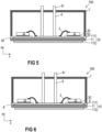
Figures 4 ,5 and 6 schematically illustrate a method for producing a seal for a semiconductor module according to one example. -
Figure 7 is a top view of an exemplary seal for a power semiconductor module arrangement. -
Figure 8 , includingFigures 8A and 8B , is a cross-sectional view of a housing for a power semiconductor module arrangement with a seal formed thereon. -
Figure 9 , includingFigures 9A and 9B , is a cross sectional view of a sidewall of a housing with a seal formed thereon. - In the following detailed description, reference is made to the accompanying drawings. The drawings show specific examples in which the invention may be practiced. It is to be understood that the features and principles described with respect to the various examples may be combined with each other, unless specifically noted otherwise. In the description as well as in the claims, designations of certain elements as "first element", "second element", "third element" etc. are not to be understood as enumerative. Instead, such designations serve solely to address different "elements". That is, e.g., the existence of a "third element" does not require the existence of a "first element" and a "second element". An electrical line or electrical connection as described herein may be a single electrically conductive element, or include at least two individual electrically conductive elements connected in series and/or parallel. Electrical lines and electrical connections may include metal and/or semiconductor material, and may be permanently electrically conductive (i.e., non-switchable). A semiconductor body as described herein may be made from (doped) semiconductor material and may be a semiconductor chip or be included in a semiconductor chip. A semiconductor body has electrically connecting pads and includes at least one semiconductor element with electrodes.
- Referring to
Figure 1 , a cross-sectional view of a powersemiconductor module arrangement 100 is illustrated. The powersemiconductor module arrangement 100 includes ahousing 7 and asubstrate 10. Thesubstrate 10 includes adielectric insulation layer 11, a (structured)first metallization layer 111 attached to thedielectric insulation layer 11, and a (structured)second metallization layer 112 attached to thedielectric insulation layer 11. Thedielectric insulation layer 11 is disposed between the first andsecond metallization layers - Each of the first and
second metallization layers substrate 10 may be a ceramic substrate, that is, a substrate in which thedielectric insulation layer 11 is a ceramic, e.g., a thin ceramic layer. The ceramic may consist of or include one of the following materials: aluminum oxide; aluminum nitride; zirconium oxide; silicon nitride; boron nitride; or any other dielectric ceramic. For example, thedielectric insulation layer 11 may consist of or include one of the following materials: Al2O3, AlN, SiC, BeO or Si3N4. For instance, thesubstrate 10 may, e.g., be a Direct Copper Bonding (DCB) substrate, a Direct Aluminum Bonding (DAB) substrate, or an Active Metal Brazing (AMB) substrate. Further, thesubstrate 10 may be an Insulated Metal Substrate (IMS). An Insulated Metal Substrate generally comprises adielectric insulation layer 11 comprising (filled) materials such as epoxy resin or polyimide, for example. The material of thedielectric insulation layer 11 may be filled with ceramic particles, for example. Such particles may comprise, e.g., SiO2, Al2O3, AlN, or BN and may have a diameter of between about 1µm and about 50µm. Thesubstrate 10 may also be a conventional printed circuit board (PCB) having a non-ceramicdielectric insulation layer 11. For instance, a non-ceramicdielectric insulation layer 11 may consist of or include a cured resin. - The
substrate 10 is arranged in ahousing 7. In the example illustrated inFigure 1 , thesubstrate 10 forms a ground surface of thehousing 7, while thehousing 7 itself solely comprises sidewalls and a cover. This is, however, only an example. It is also possible that thesubstrate 10 is mounted on a base plate. In some powersemiconductor module arrangements 100, more than onesubstrate 10 is arranged on a single base plate. A base plate may form a ground surface of thehousing 7, for example. That is, the sidewalls of thehousing 7 may be attached to the base plate, thereby covering the at least onesubstrate 10. - One or
more semiconductor bodies 20 may be arranged on the at least onesubstrate 10. Each of thesemiconductor bodies 20 arranged on the at least onesubstrate 10 may include a diode, an IGBT (Insulated-Gate Bipolar Transistor), a MOSFET (Metal-Oxide-Semiconductor Field-Effect Transistor), a JFET (Junction Field-Effect Transistor), a HEMT (High-Electron-Mobility Transistor), or any other suitable controllable or non-controllable semiconductor element. - The one or
more semiconductor bodies 20 may form a semiconductor arrangement on thesubstrate 10. InFigure 1 , only twosemiconductor bodies 20 are exemplarily illustrated. Thesecond metallization layer 112 of thesemiconductor substrate 10 inFigure 1 is a continuous layer. It is, however, also possible to omit thesecond metallization layer 112. It is also possible that thesecond metallization layer 112 is a structured layer. Thefirst metallization layer 111 is a structured layer in the example illustrated inFigure 1 . "Structured layer" in this context means that thefirst metallization layer 111 is not a continuous layer, but includes recesses between different sections of the layer. Such recesses are schematically illustrated inFigure 1 . Thefirst metallization layer 111 in this example includes three different sections.Different semiconductor bodies 20 may be mounted on the same or to different sections of thefirst metallization layer 111. Different sections of the first metallization layer may have no electrical connection or may be electrically connected to one or more other sections using, e.g.,bonding wires 3.Electrical connections 3 may also include bonding ribbons, connection plates or conductor rails, for example, to name just a few examples. The one ormore semiconductor bodies 20 may be electrically and mechanically connected to thesubstrate 10 by an electricallyconductive connection layer 30. Such an electrically conductive connection layer may be a solder layer, a layer of an electrically conductive adhesive, or a layer of a sintered metal powder, e.g., a sintered silver powder, for example. - The power
semiconductor module arrangement 100 further includesterminal elements 4. Theterminal elements 4 are electrically connected to thefirst metallization layer 111 and provide an electrical connection between the inside and the outside of thehousing 7. Theterminal elements 4 may be electrically connected to thefirst metallization layer 111 with a first end, while asecond end 41 of theterminal elements 4 protrudes out of thehousing 7. Theterminal elements 4 may be electrically contacted from the outside at theirsecond end 41. Suchterminal elements 4, however, are only an example. The components inside thehousing 7 may be electrically contacted from outside thehousing 7 in any other suitable way. For example,terminal elements 4 may be arranged closer or adjacent to the sidewalls of thehousing 7. It is also possible thatterminal elements 4 protrude vertically or horizontally through the sidewalls of thehousing 7. It is even possible thatterminal elements 4 protrude through a ground surface of thehousing 7. - The
semiconductor bodies 20 each may include a chip pad metallization, e.g., a source, drain, anode, cathode or gate metallization. A chip pad metallization generally provides a contact surface for electrically connecting thesemiconductor body 20. The chip pad metallization may electrically contact aconnection layer 30, aterminal element 4, or anelectrical connection 3, for example. A chip pad metallization may consist of or include a metal such as aluminum, copper, gold or silver, for example. Theelectrical connections 3 and theterminal elements 4 may also consist of or include a metal such as copper, aluminum, gold, or silver, for example. - The power
semiconductor module arrangement 100 further includes a castingcompound 5. The castingcompound 5 may consist of or include a silicone gel, a silicone, polyurethane, epoxy, or polyacrylate based isolation material, or may be a rigid molding compound, for example. The castingcompound 5 may at least partly fill the interior of thehousing 7, thereby covering the components and electrical connections that are arranged on thesubstrate 10. Theterminal elements 4 may be partly embedded in the castingcompound 5. At least their second ends 41, however, are not covered by the castingcompound 5 and protrude from the castingcompound 5 through thehousing 7 to the outside of thehousing 7. The castingcompound 5 is configured to protect the components and electrical connections inside thepower semiconductor module 100, in particular inside thehousing 7, from certain environmental conditions and mechanical damage. The castingcompound 5 may be formed by dispensing a material, for example, an uncured dielectric gel, into thehousing 7, after thehousing 7 has been mounted to asubstrate 10 or to a base plate, and then curing the material. - The
housing 7 encloses the arrangement and provides further protection from certain environmental conditions and mechanical damage. As has been described above, thehousing 7 may be attached to thesubstrate 10 or, if thesubstrate 10 is arranged on a base plate, thehousing 7 may be attached to the base plate, for example. In order to prevent thecasting compound 5 from leaking out between thehousing 7 and thesubstrate 10 or base plate, and to prevent contaminants or gasses (e.g., corrosive gasses) from entering the inside of thehousing 7, aseal 8 may be arranged between thehousing 7 and the substrate 10 (or between thehousing 7 and the base plate). Referring toFigure 2 , asemiconductor module arrangement 100 comprising aseal 8 between thesubstrate 10 and thehousing 7 is schematically illustrated. - In order to form the
seal 8, the material of theseal 8 may be applied on the substrate 10 (or base plate) or to thehousing 7 in a liquid or viscous form. Thehousing 7 may then be arranged on the substrate 10 (or base plate), with the material of theseal 8 arranged between thehousing 7 and the substrate 10 (or base plate). The material of theseal 8 may then be cured, e.g., by heating the arrangement. During the curing process, the presence of contaminants may cause the formation of air bubbles and unwanted cavities in theseal 8 which may decrease the sealing abilities of theseal 8. Measurements to avoid unwanted bubble formation lead to higher costs due to additional process steps and/or longer cycle times. Furthermore, components of theviscous seal 8 can interact with other module components, especially during heating, until solidification which can have an adverse impact on the module negative, e.g., through reduced cycle times. - In addition, there is a risk that contaminants in the material forming the seal will interfere with the curing process such that non-solidified (non-cured) material remains between the housing and the cured parts of the
seal 8. This may also result in reduced sealing abilities of theseal 8. For example, corrosive gasses may be able to enter thehousing 7 through a non-solidified layer of sealing material. - It is therefore important to prevent air from penetrating into the
material 90, so theseal 8 is free of any unwanted air bubbles or cavities. Even further, any fluids or moisture that may be present in thehousing 7 should be prevented from penetrating into theseal 8. Theseal 8, therefore, should also be free of any unwanted air bubbles and uncured material. Measurements to avoid unwanted bubble formation lead to higher costs due to additional process steps and/or longer cycle times. - Now referring to
Figure 3A , a conventional process for forming a seal is schematically illustrated. The liquid or viscous material 90 (illustrated inside the box at the top ofFigure 3A ) is dispensed on the respective surface of thesubstrate 10, base plate, or housing 7 (step 301A), and, once thehousing 7 has been arranged on thesubstrate 10 or base plate, with the material 90 arranged therebetween, thematerial 90 is cured (step 302A). The material 90 generally comprises amatrix material 82, e.g., a silicone-based matrix material, and anadhesion promoter 84. Adhesion promoters, often also referred to as coupling agents, are chemicals that act at the interface between two different materials (e.g., an organic polymer such as the matrix material, and an inorganic material such as the housing, substrate and base plate) to enhance adhesion between the two materials. Organic and inorganic materials are very different in many ways, for example, compatibility, chemical reactivity, surface properties, and coefficient of thermal expansion, such that forming a strong adhesive bond between each of these two dissimilar materials and thematrix material 82 is difficult. Anadhesion promoter 84 acts effectively at the interface between thematrix material 82 and each of the organic and inorganic materials (e.g., the interface betweenmatrix material 82 andhousing 7, and the interface betweenmatrix material 82 andsubstrate 10 or base plate) to chemically and physically wed each of these dissimilar materials with thematrix material 82 via a strong cohesive bond structure. - The curing process is usually performed at temperatures that are high enough and applied for a sufficient duration to solidify (cure) the
matrix material 82 and activate theadhesion promoter 84. That is, during the curing process, a crosslinking process occurs and theadhesion promoter 84 is activated, resulting in certain adhesion properties of the resultingseal 8. Once activated, the adhesion promoter is consumed, such that it becomes unreactive, i.e. it cannot be activated again at a later time. - Now referring to
Figure 3B , a method according to one example is schematically illustrated. A material 90 comprising a silicone basedmatrix material 82 and anadhesion promoter 84 may be provided. Thematerial 90 may be the same or similar to the material 90 described with respect toFigure 3A . In a first step (step 301B), thematerial 90 is heated to a first temperature. The first temperature, however, is lower than the temperature that is required to activate theadhesion promoter 84, or is applied for a duration that is too short (insufficient) to fully consume theadhesion promoter 84. That is, the material 90 (the matrix material 82) is cured (crosslinking process occurs) while ensuring that a sufficient amount ofadhesion promoter 84 remains in the pre-seal 92 after curing. The resulting intermediate product (pre-seal 92) is solid (cured/hardened) but has limited adhesive properties, which is to say that while it might be slightly sticky, it cannot be durably attached to a surface. This makes the pre-seal 92 easy to handle. Thestep 301B which is illustrated above the dashed line inFigure 3B may be performed at a supplier of the pre-seal 92, for example. The pre-seal 92 may then be shipped to a manufacturer of the powersemiconductor module arrangement 100. A surface on which the pre-seal 92 is formed, therefore, may be a suitable working surface and the resultingpre-seal 92 may be removed from the working surface for further handling. -
Different adhesion promoters 84 may usually be suitable to be used in aseal 8. Eachadhesion promoter 84 may have a different specific activation time-temperature budget. In other words, heating a givenadhesion promoter 84 at a given temperature for a given period of time will lead to activation and consumption of thatadhesion promoter 84. On the other hand, heating thatsame adhesion promoter 84 at a higher temperature for a shorter time, or at a lower temperature for a longer time, can also lead to activation and consumption of thatadhesion promoter 84.Many adhesion promoters 84 have an activation temperature of between 130°C and 150°C, and activation times of between 20 minutes and 120 minutes. That is, the temperature and time during which thefirst step 301B is performed depends on the specific activation time-temperature budget of theadhesion promoter 84 present in thematerial 90. In any case, however, thefirst step 301B is performed for a duration and at a temperature that is lower than the activation time-temperature budget of theadhesion promoter 84 that is used for theseal 8. Thematrix material 82 that is used for a silicon basedseal 8, for example, generally cures at temperatures that are significantly lower than the activation temperature of theadhesion promoter 84. The curing may even occur at relatively low temperatures such as, e.g., between 50°C and 100°C. According to one example, a curing step (step 301B) may be performed at 50°C for 2 hours, at 60°C for 1 hour, or at 80°C for 30 minutes. As noted, however, the specific temperatures and durations generally depend on the specific materials and may vary. - The resulting
pre-seal 92 may be shipped and may then be arranged on a surface of asubstrate 10, base plate orhousing 7, and thehousing 7 may be arranged on thesubstrate 10 or base plate with the pre-seal 92 arranged therebetween (step 302B). A second heating step may follow during which the arrangement, and in particular the pre-seal 92, is heated to temperatures which correspond to or are even higher than the activation temperature of the adhesion promoter 84 (step 303B). For example, heat may be applied to the side of thesubstrate 10 or base plate opposite the side to which the pre-seal 92 is mounted, effecting activation of theadhesion promoter 84, and causing the resultingseal 8 to securely attach to both thehousing 7 and thesubstrate 10 or base plate. That is, the resultingseal 8 securely attaches thehousing 7 to thesubstrate 10 or base plate and, in addition, seals the inside of thehousing 7. - Conventional non-adhesive seals such as gaskets and o-rings can also be used to seal power modules. However, such gaskets and o-rings require use of external fasteners to provide a compressive force to maintain a seal between the
housing 7 andsubstrate 10 or base plate at all times, both before and after curing of the castingcompound 5. Again, the adhesive properties of theadhesive seal 8 according to embodiments of the disclosure mean that no additional fasteners are required after the adhesion promoter is activated so as to secure thehousing 7 to thesubstrate 10 or base plate. - The
steps Figure 3B above, are again illustrated by means ofFigures 4 ,5 and 6 . As is schematically illustrated inFigure 4 , a pre-produced pre-seal 92 may be arranged on asubstrate 10. Ahousing 7 may be arranged on thesubstrate 10, with the pre-seal 92 arranged between thesubstrate 10 and thehousing 7, as is illustrated inFigure 5 . A heating step may follow during which the adhesion promoter that is present in the pre-seal 92 (but which has not yet been activated) is activated, resulting in aseal 8 which has sealing properties as well as adhesion properties. That is, the resultingseal 8 has strong adhesion forces and securely attaches thehousing 7 to thesubstrate 10. - The pre-seal 92 may have any suitable form. According to one example, the pre-seal 92 forms a closed loop, as is schematically illustrated in
Figure 7 , for example. The shape and size of the pre-seal 92 may depend on the shape and size of thehousing 7, for example. The pre-seal 92 may have the exact same shape and dimensions as thehousing 7 such that it may be arranged between thehousing 7 and thesubstrate 10 or base plate to attach thehousing 7 to thesubstrate 10 or base plate and seal the inside of thehousing 7.Many substrates 10, base plates andhousings 7 have a rectangular or square shape. Other shapes, however, are generally possible. The size of the pre-seal 92 may be slightly smaller than the size of therespective substrate 10 or base plate such that, when it is arranged on thesubstrate 10 or base plate, it extends along its edge. When thehousing 7 is arranged on the pre-seal 92, the pre-seal 92 extends along the entire circumference of the housing 7 (i.e., along the lower surface of the sidewalls of thehousing 7 that face towards thesubstrate 10 or base plate). - Alternatively, the pre-seal 92 may be arranged on a surface of the
housing 7 first. Thehousing 7 with the pre-seal 92 arranged thereon may then be arranged on asubstrate 10. The heating step may follow as has been described above with respect toFigure 6 to form thefinal seal 8. If thesubstrate 10 is arranged on a base plate, thehousing 7 may be arranged on the base plate, with the pre-seal 92 arranged between the base plate and thehousing 7. - It is possible to manufacture and ship the pre-seal 92 independently. According to another example, however, it is also possible to form the pre-seal 92 on the
housing 7 and ship thehousing 7 together with the pre-seal 92 formed thereon. This is schematically illustrated inFigure 8 . In a first step, thematerial 90 including the (silicone based) matrix material and the adhesion promoter may be applied to the housing 7 (e.g., on a lower surface of the sidewalls of thehousing 7 that face towards thesubstrate 10 or base plate when thehousing 7 is arranged on thesubstrate 10 or base plate). This is schematically illustrated inFigure 8A . A heating step is performed to cure the matrix material without activating or without fully consuming the adhesion promoter, thereby forming the pre-seal 92 (Figure 8B ). Thehousing 7 with the pre-seal 92 formed thereon may then be arranged on asubstrate 10 or base plate and thefinal seal 8 may be formed by performing the second heating step as has been described above. - The lower surface of the sidewalls of the
housing 7 may be a flat or essentially flat surface, as is schematically illustrated inFigure 8 , for example. In this case, the pre-seal 92 is required to have certain adhesive properties in order to remain attached to the flat lower surface. It is, however, also possible that the lower surface of the sidewalls is formed to have at least one recess or undercut 72, for example. This is schematically illustrated inFigure 9A . When thematerial 90 is applied to the lower surface of thehousing 7, thematerial 90 fills therecess 72 formed in the sidewall of thehousing 7, and further forms a layer ofmaterial 90 that extends from the lower surface in a vertical direction y. Once thematerial 90 has been cured and the pre-seal 92 is solid, it is securely attached to the lower surface of thehousing 7 without having any adhesive properties yet, or having only limited adhesive properties. The specific form of therecess 72 illustrated inFigure 9A is merely an example. A recess or undercut 72 may generally have any suitable form. In this case, the pre-seal 92 remains attached to the sidewall of the housing without having any adhesive properties. - A similar effect may be achieved if the lower surface of the
housing 7 comprises aprotrusion 74, and thematerial 90 is applied to the lower surface of thehousing 7 such that it forms a layer ofmaterial 90 that extends from the lower surface in a vertical direction y and entirely encloses theprotrusion 74, as is exemplarily illustrated inFigure 9B . Therecess 72 orprotrusion 74 may be acontinuous recess 72 orprotrusion 74 along the entire circumference of thehousing 7. It is, however, also possible, that a plurality ofrecesses 72 and/orprotrusions 74 is arranged along the circumference of thehousing 7. - When forming a pre-seal 92 (either independently or on a lower surface of the housing, for example), the curing step at a temperature below the activation temperature of the
adhesion promoter 84 may be carried out in a vacuum chamber, for example. This prevents air from penetrating into thematerial 90. The resulting pre-seal 92 as well as thefinal seal 8, therefore, are free of any unwanted air bubbles or cavities. Even further, any fluids or moisture that may be present in thehousing 7 may be prevented from penetrating into thematerial 90. The resulting pre-seal 92 as well as thefinal seal 8, therefore, are also free of any unwanted fluids. - According to another example, a
housing 7 with a pre-attached pre-seal 92 may be formed in a two-shot (2K) injection molding process, for example. Techniques that are known as 2K injection molding allow to form injection-molded parts comprising two different materials in the same mold. A first material (e.g., the material forming the housing 7) may be filled into a mold by means of at least one injection. At least one second injection is used to fill a second material (e.g., thematerial 90 forming the pre-seal 92) into a mold containing thehousing 7, where the mold has defined locations adjacent thehousing 7. The two materials, in this way, may be connected to each other. It is important that during the second step of the 2K processes, e.g., during formation of the pre-seal 92, that the temperature be held sufficiently high and for a sufficient time to allow curing of thesecond material 90 but at a low enough temperature and/or for a time that is short enough to prevent the adhesion promoter from being fully consumed during the curing process. The 2K injection molding process can be a manual two-step process, or a fully automated process using a rotary injection molding form, for example. The two materials may be filled into the mold in any suitable order, as long as the temperature can be held low enough or for an amount of time insufficient to allow full consumption of the adhesion promoter in thepre-seal material 90. - According to this example, the housing/
pre-seal assembly substrate 10 by placing it on thesubstrate 10 with the pre-seal 92 arranged between thehousing 7 and thesubstrate 10 and by pressing thehousing 7 toward the substrate. The pre-seal 92 is then heated in order to activate the adhesion promoter remaining in thepre-seal material 90, for example, by heating the other side of thesubstrate 10. Pressure may be removed from thehousing 7 and the heat may be removed once the adhesion promoter is fully activated and the pre-seal 92 seal is fully adhered to thesubstrate 10 - It is generally also possible to form a pre-seal 92 on a
substrate 10 or base plate, similar to what has been described with respect to thehousing 7 above. Ahousing 7 may then be arranged on thesubstrate 10 or base plate with the pre-seal 92 arranged between thehousing 7 and thesubstrate 10 or base plate. Thefinal seal 8 may be formed by performing the second heating step as has been described above.
Claims (12)
- A method comprising:applying a first material (90) to a first surface, the first material (90) comprising a matrix material (82) and an adhesion promoter (94), wherein the matrix material (82) is configured to cure when heated to a defined temperature for a defined period of time, and wherein the adhesion promoter (84) is configured to be activated when heated to a temperature that is higher than the defined temperature and/or for a period of time that is longer than the defined period of time; andheating the first material (90) to the defined temperature for the defined period of time such that the matrix material (82) cures and the adhesion promoter (84) remains inactive, thereby forming a pre-seal (92).
- The method of claim 1, further comprisingremoving the pre-seal (92) from the first surface;arranging the pre-seal (92) between a housing (7) and a substrate (10) or a base plate of a power semiconductor module; andheating the pre-seal (92) to a temperature that is equal to the defined temperature for a period of time that is longer than the defined period of time, or to a temperature that is greater than the defined temperature for a period of time that equals or is longer than the defined period of time, thereby activating the adhesion promoter (94) and forming a seal (8) between the housing (7) and the substrate (10) or base plate, the seal (8) forming an adhesive bond with the housing (7) and with the substrate (10) or base plate.
- The method of claim 1, wherein the first surface is a surface of a housing (7), and the method further comprisesarranging the housing (7) with the pre-seal (92) arranged thereon on a substrate (10) or base plate; andheating the pre-seal (92) to a temperature that is equal to the defined temperature for a period of time that is longer than the defined period of time, or to a temperature that is greater than the defined temperature for a period of time that equals or is longer than the defined period of time, thereby activating the adhesion promoter (94) and forming a seal (8) between the housing (7) and the substrate (10) or base plate, the seal (8) forming an adhesive bond with the housing (7) and with the substrate (10) or base plate.
- The method of claim 3, further comprisingfilling a material different from the first material (90) into a mold to form the housing (7), whereinapplying the first material (90) to the first surface comprises subsequently filling the first material (90) into the mold.
- The method of claim 3 or 4, whereinthe surface of the housing (7) comprises at least one recess (72), and the first material (90) is applied to the surface such that it fills the at least one recess (72) and forms a layer of material (90) that extends from the surface in a vertical direction (y); and/orthe surface of the housing (7) comprises at least one protrusion (74), and the first material (90) is applied to the surface such that it forms a layer of material (90) that extends from the surface in a vertical direction (y) and entirely encloses the at least one protrusion (74).
- The method of claim 1, wherein the first surface is a surface of a substrate (10) or base plate, and the method further comprisesarranging a housing (7) on the substrate (10) or base plate such that the pre-seal (92) is arranged between the housing (7) and the substrate (10) or base plate; andheating the pre-seal (92) to a temperature that is equal to the defined temperature for a period of time that is longer than the defined period of time, or to a temperature that is greater than the defined temperature for a period of time that equals or is longer than the defined period of time, thereby activating the adhesion promoter (94) and forming a seal (8) between the housing (7) and the substrate (10) or base plate, the seal (8) forming an adhesive bond with the housing (7) and with the substrate (10) or base plate.
- The method of any of claims 1 to 6, wherein the matrix material (82) is a silicone based matrix material.
- The method of any of the preceding claims, whereinthe defined temperature is between 50°C and 100°C; andheating the pre-seal (92) to a temperature that is greater than the defined temperature comprises heating the pre-seal (92) to a temperature of between 130°C and 150°C.
- The method of any of claims 2 to 8, wherein the pre-seal (92) is arranged between the housing (7) and the substrate (10) or base plate such that it extends along the entire circumference of the housing (7) along a lower surface of the sidewalls of the housing 7 that face towards the substrate (10) or base plate.
- The method of any of the preceding claims, wherein the pre-seal (92) forms a closed loop.
- A housing (7) for a power semiconductor module arrangement (100), the housing comprising:sidewalls and a cover; anda pre-seal (92) arranged on a lower surface of the sidewalls, wherein the pre-seal (92) comprises a cured matrix material (82) and an uncured adhesion promoter (84).
- The housing (7) of claim 11, whereinthe lower surface of the housing (7) comprises at least one recess (72), and the pre-seal (92) fills the at least one recess (72) and forms a layer that extends from the lower surface in a vertical direction (y); and/orthe surface of the housing (7) comprises at least one protrusion (74), and pre-seal (92) forms a layer that extends from the lower surface in a vertical direction (y) and entirely encloses the at least one protrusion (74).
Priority Applications (3)
| Application Number | Priority Date | Filing Date | Title |
|---|---|---|---|
| EP23177665.9A EP4475167B1 (en) | 2023-06-06 | 2023-06-06 | Methods for producing a seal for a semiconductor module, and a housing for a semiconductor module |
| CN202410705160.XA CN119092418A (en) | 2023-06-06 | 2024-06-03 | Method for producing a seal for a semiconductor module and housing for a semiconductor module |
| US18/732,716 US20240413025A1 (en) | 2023-06-06 | 2024-06-04 | Methods for producing a seal for a semiconductor module, and a housing for a semiconductor module |
Applications Claiming Priority (1)
| Application Number | Priority Date | Filing Date | Title |
|---|---|---|---|
| EP23177665.9A EP4475167B1 (en) | 2023-06-06 | 2023-06-06 | Methods for producing a seal for a semiconductor module, and a housing for a semiconductor module |
Publications (2)
| Publication Number | Publication Date |
|---|---|
| EP4475167A1 true EP4475167A1 (en) | 2024-12-11 |
| EP4475167B1 EP4475167B1 (en) | 2025-07-30 |
Family
ID=86732332
Family Applications (1)
| Application Number | Title | Priority Date | Filing Date |
|---|---|---|---|
| EP23177665.9A Active EP4475167B1 (en) | 2023-06-06 | 2023-06-06 | Methods for producing a seal for a semiconductor module, and a housing for a semiconductor module |
Country Status (3)
| Country | Link |
|---|---|
| US (1) | US20240413025A1 (en) |
| EP (1) | EP4475167B1 (en) |
| CN (1) | CN119092418A (en) |
Citations (2)
| Publication number | Priority date | Publication date | Assignee | Title |
|---|---|---|---|---|
| US6428650B1 (en) * | 1998-06-23 | 2002-08-06 | Amerasia International Technology, Inc. | Cover for an optical device and method for making same |
| US20220344236A1 (en) * | 2021-04-27 | 2022-10-27 | NGK Electronics Devices, Inc. | Package and electronic device |
-
2023
- 2023-06-06 EP EP23177665.9A patent/EP4475167B1/en active Active
-
2024
- 2024-06-03 CN CN202410705160.XA patent/CN119092418A/en active Pending
- 2024-06-04 US US18/732,716 patent/US20240413025A1/en active Pending
Patent Citations (2)
| Publication number | Priority date | Publication date | Assignee | Title |
|---|---|---|---|---|
| US6428650B1 (en) * | 1998-06-23 | 2002-08-06 | Amerasia International Technology, Inc. | Cover for an optical device and method for making same |
| US20220344236A1 (en) * | 2021-04-27 | 2022-10-27 | NGK Electronics Devices, Inc. | Package and electronic device |
Also Published As
| Publication number | Publication date |
|---|---|
| US20240413025A1 (en) | 2024-12-12 |
| EP4475167B1 (en) | 2025-07-30 |
| CN119092418A (en) | 2024-12-06 |
Similar Documents
| Publication | Publication Date | Title |
|---|---|---|
| CN109659284B (en) | Semiconductor device with a plurality of semiconductor chips | |
| CN105405815A (en) | Semiconductor device and manufacturing method thereof | |
| US9536802B2 (en) | Semiconductor device | |
| CN104465412A (en) | Method Of Manufacturing A Chip Package, Chip Package, Method Of Manufacturing A Chip Assembly And Chip Assembly | |
| CN108604589B (en) | Semiconductor device and method for manufacturing the same | |
| EP4050645B1 (en) | Power semiconductor device and manufacturing method | |
| CN107112318A (en) | power module | |
| US8841166B2 (en) | Manufacturing method of semiconductor device, and semiconductor device | |
| CN108292655A (en) | Power module | |
| JP2021111700A (en) | Semiconductor module and manufacturing method of the same | |
| CN114078790B (en) | Power semiconductor module device and manufacturing method thereof | |
| US20220157673A1 (en) | Module-type semiconductor device and method of manufacturing module-type semiconductor device | |
| EP4475167B1 (en) | Methods for producing a seal for a semiconductor module, and a housing for a semiconductor module | |
| US12261063B2 (en) | Method and device for producing a housing | |
| EP4270469A1 (en) | Power semiconductor module | |
| EP4307359A1 (en) | Power semiconductor module arrangement and method for producing the same | |
| CN110634751A (en) | Packaging method and packaging structure of a power semiconductor module | |
| WO2023073831A1 (en) | Semiconductor device and method for manufacturing semiconductor device | |
| EP4478400A1 (en) | Methods for forming a power semiconductor module arrangement | |
| EP4651201A1 (en) | Power semiconductor module arrangement and methods for producing the same | |
| EP4604176A1 (en) | Semiconductor module arrangement, electronics carrier for a semiconductor module arrangement, and method for producing a semiconductor module arrangement | |
| EP3428954B1 (en) | Method for establishing a connection between two joining partners | |
| US20260053056A1 (en) | Housing and semiconductor module having a housing | |
| EP4489067B1 (en) | Housing, semiconductor module and methods for producing the same | |
| EP4276888A1 (en) | Method for producing a power semiconductor module |
Legal Events
| Date | Code | Title | Description |
|---|---|---|---|
| PUAI | Public reference made under article 153(3) epc to a published international application that has entered the european phase |
Free format text: ORIGINAL CODE: 0009012 |
|
| STAA | Information on the status of an ep patent application or granted ep patent |
Free format text: STATUS: REQUEST FOR EXAMINATION WAS MADE |
|
| 17P | Request for examination filed |
Effective date: 20240405 |
|
| AK | Designated contracting states |
Kind code of ref document: A1 Designated state(s): AL AT BE BG CH CY CZ DE DK EE ES FI FR GB GR HR HU IE IS IT LI LT LU LV MC ME MK MT NL NO PL PT RO RS SE SI SK SM TR |
|
| GRAP | Despatch of communication of intention to grant a patent |
Free format text: ORIGINAL CODE: EPIDOSNIGR1 |
|
| STAA | Information on the status of an ep patent application or granted ep patent |
Free format text: STATUS: GRANT OF PATENT IS INTENDED |
|
| RIC1 | Information provided on ipc code assigned before grant |
Ipc: H01L 25/07 20060101ALN20250224BHEP Ipc: H01L 23/498 20060101ALN20250224BHEP Ipc: H01L 23/24 20060101ALN20250224BHEP Ipc: H01L 23/053 20060101ALN20250224BHEP Ipc: H01L 23/10 20060101ALI20250224BHEP Ipc: H01L 21/50 20060101AFI20250224BHEP |
|
| RIC1 | Information provided on ipc code assigned before grant |
Ipc: H01L 25/07 20060101ALN20250320BHEP Ipc: H01L 23/498 20060101ALN20250320BHEP Ipc: H01L 23/24 20060101ALN20250320BHEP Ipc: H01L 23/053 20060101ALN20250320BHEP Ipc: H01L 23/10 20060101ALI20250320BHEP Ipc: H01L 21/50 20060101AFI20250320BHEP |
|
| INTG | Intention to grant announced |
Effective date: 20250401 |
|
| GRAS | Grant fee paid |
Free format text: ORIGINAL CODE: EPIDOSNIGR3 |
|
| GRAA | (expected) grant |
Free format text: ORIGINAL CODE: 0009210 |
|
| STAA | Information on the status of an ep patent application or granted ep patent |
Free format text: STATUS: THE PATENT HAS BEEN GRANTED |
|
| P01 | Opt-out of the competence of the unified patent court (upc) registered |
Free format text: CASE NUMBER: APP_24604/2025 Effective date: 20250522 |
|
| AK | Designated contracting states |
Kind code of ref document: B1 Designated state(s): AL AT BE BG CH CY CZ DE DK EE ES FI FR GB GR HR HU IE IS IT LI LT LU LV MC ME MK MT NL NO PL PT RO RS SE SI SK SM TR |
|
| REG | Reference to a national code |
Ref country code: GB Ref legal event code: FG4D |
|
| REG | Reference to a national code |
Ref country code: CH Ref legal event code: EP |
|
| REG | Reference to a national code |
Ref country code: DE Ref legal event code: R096 Ref document number: 602023005156 Country of ref document: DE |
|
| REG | Reference to a national code |
Ref country code: IE Ref legal event code: FG4D |
|
| REG | Reference to a national code |
Ref country code: DE Ref legal event code: R079 Ref document number: 602023005156 Country of ref document: DE Free format text: PREVIOUS MAIN CLASS: H01L0021500000 Ipc: H10W0076010000 |
|
| REG | Reference to a national code |
Ref country code: NL Ref legal event code: MP Effective date: 20250730 |
|
| REG | Reference to a national code |
Ref country code: AT Ref legal event code: MK05 Ref document number: 1819997 Country of ref document: AT Kind code of ref document: T Effective date: 20250730 |
|
| PG25 | Lapsed in a contracting state [announced via postgrant information from national office to epo] |
Ref country code: PT Free format text: LAPSE BECAUSE OF FAILURE TO SUBMIT A TRANSLATION OF THE DESCRIPTION OR TO PAY THE FEE WITHIN THE PRESCRIBED TIME-LIMIT Effective date: 20251202 |
|
| PG25 | Lapsed in a contracting state [announced via postgrant information from national office to epo] |
Ref country code: IS Free format text: LAPSE BECAUSE OF FAILURE TO SUBMIT A TRANSLATION OF THE DESCRIPTION OR TO PAY THE FEE WITHIN THE PRESCRIBED TIME-LIMIT Effective date: 20251130 |
|
| PG25 | Lapsed in a contracting state [announced via postgrant information from national office to epo] |
Ref country code: NO Free format text: LAPSE BECAUSE OF FAILURE TO SUBMIT A TRANSLATION OF THE DESCRIPTION OR TO PAY THE FEE WITHIN THE PRESCRIBED TIME-LIMIT Effective date: 20251030 |
|
| REG | Reference to a national code |
Ref country code: LT Ref legal event code: MG9D |
|
| PG25 | Lapsed in a contracting state [announced via postgrant information from national office to epo] |
Ref country code: AT Free format text: LAPSE BECAUSE OF FAILURE TO SUBMIT A TRANSLATION OF THE DESCRIPTION OR TO PAY THE FEE WITHIN THE PRESCRIBED TIME-LIMIT Effective date: 20250730 |
|
| PG25 | Lapsed in a contracting state [announced via postgrant information from national office to epo] |
Ref country code: FI Free format text: LAPSE BECAUSE OF FAILURE TO SUBMIT A TRANSLATION OF THE DESCRIPTION OR TO PAY THE FEE WITHIN THE PRESCRIBED TIME-LIMIT Effective date: 20250730 |
|
| PG25 | Lapsed in a contracting state [announced via postgrant information from national office to epo] |
Ref country code: HR Free format text: LAPSE BECAUSE OF FAILURE TO SUBMIT A TRANSLATION OF THE DESCRIPTION OR TO PAY THE FEE WITHIN THE PRESCRIBED TIME-LIMIT Effective date: 20250730 Ref country code: NL Free format text: LAPSE BECAUSE OF FAILURE TO SUBMIT A TRANSLATION OF THE DESCRIPTION OR TO PAY THE FEE WITHIN THE PRESCRIBED TIME-LIMIT Effective date: 20250730 |
|
| PG25 | Lapsed in a contracting state [announced via postgrant information from national office to epo] |
Ref country code: GR Free format text: LAPSE BECAUSE OF FAILURE TO SUBMIT A TRANSLATION OF THE DESCRIPTION OR TO PAY THE FEE WITHIN THE PRESCRIBED TIME-LIMIT Effective date: 20251031 |
|
| PG25 | Lapsed in a contracting state [announced via postgrant information from national office to epo] |
Ref country code: SE Free format text: LAPSE BECAUSE OF FAILURE TO SUBMIT A TRANSLATION OF THE DESCRIPTION OR TO PAY THE FEE WITHIN THE PRESCRIBED TIME-LIMIT Effective date: 20250730 |
|
| PG25 | Lapsed in a contracting state [announced via postgrant information from national office to epo] |
Ref country code: LV Free format text: LAPSE BECAUSE OF FAILURE TO SUBMIT A TRANSLATION OF THE DESCRIPTION OR TO PAY THE FEE WITHIN THE PRESCRIBED TIME-LIMIT Effective date: 20250730 |
|
| PG25 | Lapsed in a contracting state [announced via postgrant information from national office to epo] |
Ref country code: PL Free format text: LAPSE BECAUSE OF FAILURE TO SUBMIT A TRANSLATION OF THE DESCRIPTION OR TO PAY THE FEE WITHIN THE PRESCRIBED TIME-LIMIT Effective date: 20250730 Ref country code: BG Free format text: LAPSE BECAUSE OF FAILURE TO SUBMIT A TRANSLATION OF THE DESCRIPTION OR TO PAY THE FEE WITHIN THE PRESCRIBED TIME-LIMIT Effective date: 20250730 |
|
| PG25 | Lapsed in a contracting state [announced via postgrant information from national office to epo] |
Ref country code: RS Free format text: LAPSE BECAUSE OF FAILURE TO SUBMIT A TRANSLATION OF THE DESCRIPTION OR TO PAY THE FEE WITHIN THE PRESCRIBED TIME-LIMIT Effective date: 20251030 |
|
| PG25 | Lapsed in a contracting state [announced via postgrant information from national office to epo] |
Ref country code: ES Free format text: LAPSE BECAUSE OF FAILURE TO SUBMIT A TRANSLATION OF THE DESCRIPTION OR TO PAY THE FEE WITHIN THE PRESCRIBED TIME-LIMIT Effective date: 20250730 |
|
| PG25 | Lapsed in a contracting state [announced via postgrant information from national office to epo] |
Ref country code: SM Free format text: LAPSE BECAUSE OF FAILURE TO SUBMIT A TRANSLATION OF THE DESCRIPTION OR TO PAY THE FEE WITHIN THE PRESCRIBED TIME-LIMIT Effective date: 20250730 |
|
| PG25 | Lapsed in a contracting state [announced via postgrant information from national office to epo] |
Ref country code: DK Free format text: LAPSE BECAUSE OF FAILURE TO SUBMIT A TRANSLATION OF THE DESCRIPTION OR TO PAY THE FEE WITHIN THE PRESCRIBED TIME-LIMIT Effective date: 20250730 |
|
| PG25 | Lapsed in a contracting state [announced via postgrant information from national office to epo] |
Ref country code: IT Free format text: LAPSE BECAUSE OF FAILURE TO SUBMIT A TRANSLATION OF THE DESCRIPTION OR TO PAY THE FEE WITHIN THE PRESCRIBED TIME-LIMIT Effective date: 20250730 |
|
| PG25 | Lapsed in a contracting state [announced via postgrant information from national office to epo] |
Ref country code: CZ Free format text: LAPSE BECAUSE OF FAILURE TO SUBMIT A TRANSLATION OF THE DESCRIPTION OR TO PAY THE FEE WITHIN THE PRESCRIBED TIME-LIMIT Effective date: 20250730 |
|
| PG25 | Lapsed in a contracting state [announced via postgrant information from national office to epo] |
Ref country code: SK Free format text: LAPSE BECAUSE OF FAILURE TO SUBMIT A TRANSLATION OF THE DESCRIPTION OR TO PAY THE FEE WITHIN THE PRESCRIBED TIME-LIMIT Effective date: 20250730 Ref country code: EE Free format text: LAPSE BECAUSE OF FAILURE TO SUBMIT A TRANSLATION OF THE DESCRIPTION OR TO PAY THE FEE WITHIN THE PRESCRIBED TIME-LIMIT Effective date: 20250730 |