EP4474891A1 - Optical transmission path and optical connector - Google Patents
Optical transmission path and optical connector Download PDFInfo
- Publication number
- EP4474891A1 EP4474891A1 EP22924058.5A EP22924058A EP4474891A1 EP 4474891 A1 EP4474891 A1 EP 4474891A1 EP 22924058 A EP22924058 A EP 22924058A EP 4474891 A1 EP4474891 A1 EP 4474891A1
- Authority
- EP
- European Patent Office
- Prior art keywords
- optical
- modulation element
- signal light
- optical waveguide
- transmission path
- Prior art date
- Legal status (The legal status is an assumption and is not a legal conclusion. Google has not performed a legal analysis and makes no representation as to the accuracy of the status listed.)
- Pending
Links
Images


Classifications
-
- G—PHYSICS
- G02—OPTICS
- G02F—OPTICAL DEVICES OR ARRANGEMENTS FOR THE CONTROL OF LIGHT BY MODIFICATION OF THE OPTICAL PROPERTIES OF THE MEDIA OF THE ELEMENTS INVOLVED THEREIN; NON-LINEAR OPTICS; FREQUENCY-CHANGING OF LIGHT; OPTICAL LOGIC ELEMENTS; OPTICAL ANALOGUE/DIGITAL CONVERTERS
- G02F1/00—Devices or arrangements for the control of the intensity, colour, phase, polarisation or direction of light arriving from an independent light source, e.g. switching, gating or modulating; Non-linear optics
- G02F1/01—Devices or arrangements for the control of the intensity, colour, phase, polarisation or direction of light arriving from an independent light source, e.g. switching, gating or modulating; Non-linear optics for the control of the intensity, phase, polarisation or colour
- G02F1/0136—Devices or arrangements for the control of the intensity, colour, phase, polarisation or direction of light arriving from an independent light source, e.g. switching, gating or modulating; Non-linear optics for the control of the intensity, phase, polarisation or colour for the control of polarisation, e.g. state of polarisation [SOP] control, polarisation scrambling, TE-TM mode conversion or separation
-
- G—PHYSICS
- G02—OPTICS
- G02F—OPTICAL DEVICES OR ARRANGEMENTS FOR THE CONTROL OF LIGHT BY MODIFICATION OF THE OPTICAL PROPERTIES OF THE MEDIA OF THE ELEMENTS INVOLVED THEREIN; NON-LINEAR OPTICS; FREQUENCY-CHANGING OF LIGHT; OPTICAL LOGIC ELEMENTS; OPTICAL ANALOGUE/DIGITAL CONVERTERS
- G02F2203/00—Function characteristic
- G02F2203/50—Phase-only modulation
Definitions
- the present invention relates to an optical transmission path including an optical waveguide.
- the present invention relates to an optical connector for connecting an optical processor and an optical waveguide.
- optical processors that optically perform computing are underway in order to surpass limits of electrical processors, such as a central processing unit (CPU) and a graphics processing unit (GPU), which electrically perform computing.
- electrical processors such as a central processing unit (CPU) and a graphics processing unit (GPU), which electrically perform computing.
- Using such optical processors enables computing to be performed at higher speed than electrical processors.
- technologies contributing to achieving such optical processors include an optical transistor disclosed in Non-Patent Literature 1. Citation List
- Non-patent Literature 1 Nozaki, K., Matsuo, S., Fujii, T. et al. Femtofarad optoelectronic integration demonstrating energy-saving signal conversion and nonlinear functions. Nat. Photonics 13, 454-459 (2019). https://doi.org/10.1038/s41566-019-0397-3
- some optical processors output optical signals that express two-dimensional data, such as images, through two-dimensional intensity distributions.
- an optical processor is connected via an electrical transmission path, it is required to (1) read two-dimensional data of m rows ⁇ n columns indicated by an optical signal, (2) generate m pieces of one-dimensional data corresponding to the rows of the two-dimensional data thus read, (3) generate m electrical signals indicating the respective m pieces of one-dimensional data thus generated, and (4) sequentially transmit the m electrical signals thus generated.
- an optical processor is connected preferably via an optical transmission path, not via an electrical transmission path.
- An aspect of the present invention is achieved in light of the foregoing problem, and it is an object of the aspect to achieve an optical transmission path that enables compensating for a change in two-dimensional intensity distribution of signal light which occurs in an optical waveguide.
- a configuration is employed of including: an optical waveguide; and an optical modulation element that has a plurality of cells having respective phase-modulation amounts set independently of each other and that has one main surface provided so as to face one end surface of the optical waveguide, wherein the respective phase-modulation amounts of the plurality of cells which constitute the optical modulation element are set so as to compensate for a change in two-dimensional intensity distribution of signal light, the change occurring in the optical waveguide.
- a configuration is employed of including: an optical waveguide; an optical modulation element that has a plurality of cells having respective phase-modulation amounts which are able to be set independently of each other and that has one main surface provided so as to face one end surface of the optical waveguide; and a control part configured to set the respective phase-modulation amounts of the plurality of cells which constitute the optical modulation element so as to compensate for a change in two-dimensional intensity distribution of signal light, the change occurring in the optical waveguide.
- An optical connector in accordance with an aspect of the present invention is an optical connector for connecting an optical waveguide and an optical processor, and in the optical connector, a configuration is employed of including: an optical modulation element that has a plurality of cells having respective phase-modulation amounts set independently of each other and that has one main surface provided so as to face one end surface of the optical waveguide, wherein the respective phase-modulation amounts of the plurality of cells which constitute the optical modulation element are set so as to compensate for a change in two-dimensional intensity distribution of signal light, the change occurring in the optical waveguide.
- An optical connector in accordance with another aspect of the present invention is an optical connector for connecting an optical waveguide and an optical processor, and in the optical connector, a configuration is employed of including an optical modulation element that has a plurality of cells having respective phase-modulation amounts which are able to be set independently of each other and that has one main surface provided so as to face one end surface of the optical waveguide; and a control part configured to set the respective phase-modulation amounts of the plurality of cells which constitute the optical modulation element so as to compensate for a change in two-dimensional intensity distribution of signal light, the change occurring in the optical waveguide.
- an optical transmission path that enables compensating for a change in two-dimensional intensity distribution of signal light which occurs in an optical waveguide.
- FIG. 1 is a perspective view illustrating a configuration of the optical transmission path 1.
- the optical transmission path 1 is a transmission path configured to transmit signal light.
- the optical transmission path 1 is used for, for example, connection between boards in which two optical processors mounted on different boards are connected or connection within a board in which two optical processors mounted on the same board are connected.
- the optical transmission path 1 includes an optical waveguide 11 and an optical modulation element group 12.
- the optical waveguide 11 is a unit configured to guide signal light.
- an optical fiber or a board-type optical waveguide for example, silicon waveguide
- an optical fiber is used as the optical waveguide 11 as the optical waveguide 11.
- the optical modulation element group 12 is a unit configured to compensate for a change in two-dimensional intensity distribution of signal light which occurs during a process of guiding the signal light in the optical waveguide 11.
- the optical modulation element group 12 is constituted by at least one optical modulation element.
- an optical modulation element group constituted by four optical modulation elements 121 to 124 is used as the optical modulation element group 12.
- each of the optical modulation elements 121 to 124 is constituted by a plurality of cells having respective phase-modulation amounts that can be set independently of each other.
- the optical modulation element 121 is provided in a manner such that one main surface 121a thereof faces one end surface 11a of the optical waveguide 11.
- the optical modulation element 122 is provided between the optical modulation element 121 and the optical waveguide 11 as in the case of the optical modulation element 121.
- the optical modulation element 123 is provided between the optical modulation element 122 and the optical waveguide 11 as in the case of the optical modulation element 121.
- the optical modulation element 124 is provided between the optical modulation element 123 and the optical waveguide 11 as in the case of the optical modulation element 121.
- signal light Li to be inputted from an optical processor into the optical transmission path 1 passes through the optical modulation element 121, the optical modulation element 122, the optical modulation element 123, and the optical modulation element 124 in this order and then is inputted from the end surface 11a into the optical waveguide 11.
- the respective phase-modulation amounts of the cells of the optical modulation elements 121 to 124 are set so as to compensate for a change in two-dimensional intensity distribution of signal light which occurs during a process of guiding the signal light in the optical waveguide 11.
- the phase-modulation amounts are set such that a difference between the two-dimensional intensity distribution of the signal light Li which enters the other main surface 121b of the optical modulation element 121 and the two-dimensional intensity distribution of signal light Lo which is emitted from the other end surface 11b of the optical waveguide 11 becomes smaller than in a case where the optical modulation element group 12 is absent.
- phase-modulation amounts of the cells of the optical modulation elements 121 to 124 for example, through machine learning.
- machine learning it is possible to use, for example, a model in which a two-dimensional intensity distribution of the signal light Li which enters the main surface 121b of the optical modulation element 121 is an input and a two-dimensional intensity distribution of the signal light Lo which is emitted from the end surface 11b of the optical waveguide 11 is an output and which includes a phase-modulation amount of each of the cells of the optical modulation elements 121 to 124 as a parameter.
- phase-modulation amounts of the cells of the optical modulation elements 121 to 124 by repeating a process of updating the parameter of the model for various signal light (training data) so as to diminish a difference between the input and the output of the model.
- an antireflection film AR may be formed on the end surface 11a of the optical waveguide 11. This makes it possible to reduce a risk that signal light that has been emitted from the optical modulation element group 12 is reflected by the end surface 11a of the optical waveguide 11 and enters the optical modulation element group 12 again.
- the optical transmission path 1 preferably includes a control part (not shown) configured to set the phase-modulation amounts of the cells of the optical modulation elements 121 to 124 as described above.
- optical modulation elements 121 to 124 are used for the compensation described above, this should not be construed as a limitation.
- the optical modulation elements 121 to 124 may be integrated together.
- four light diffraction layers formed inside a structure that allows signal light to pass therethrough, such as a dried gel may be used as the optical modulation elements 121 to 124.
- a gel that is subjected to dehydration shrinkage so that the gel shrinks while keeping a similar shape, e.g., a gel used in the Implosion Fabrication process. This makes it possible to, by drying a swollen gel in which four light diffraction layers are formed, easily manufacture the optical modulation element group 12 in which the optical modulation elements 121 to 124 are accurately arranged.
- FIG. 2 With reference to Fig. 2 , the following description will discuss the function of the optical modulation element group 12 in the optical transmission path 1.
- (a) of Fig. 2 indicates a specific example of the two-dimensional intensity distribution of the signal light Li which enters the optical modulation element 121
- (b), (c), and (d) of Fig. 2 each indicate a specific example of a cross-sectional structure of the optical waveguide 11.
- the two-dimensional intensity distribution of the signal light L1 has a cell structure of 4 ⁇ 4, as shown in (a) of Fig. 2 .
- the optical waveguide 11 has one core 111 having a cross-sectional area substantially equal to a beam cross-sectional area of the signal light Li.
- the entire signal light Li is coupled to the core 111 of the optical waveguide 11. Therefore, the two-dimensional intensity distribution of the signal light Li changes mainly by the signal light Li being guided in the core 111.
- causes of the change is the following situation: the beams of the signal light Li which have been emitted from the cells of the optical modulation element 124 and are propagating inside the core 111 while dispersing interfere with each other and are totally reflected on an interface between the core 111 and a clad 112, so that the two-dimensional intensity distribution becomes out of shape.
- the phase-modulation amounts of the cells of the optical modulation elements 121 to 124 are set so as to compensate for this change. Therefore, the two-dimensional intensity distribution of the signal light Lo which is outputted from the end surface 11b of the optical waveguide 11 becomes closer to the two-dimensional intensity distribution of the signal light Li which is inputted into the main surface 121b of the optical modulation element 121 than in a case where the optical modulation element group 12 is absent.
- the optical waveguide 11 has 16 cores 111 each having a cross-sectional area approximately one sixteenth the beam cross-sectional area of the signal light Li.
- the signal light Li for one cell is coupled to each of the cores 111 of the optical waveguide 11. Therefore, the two-dimensional intensity distribution of the signal light Li changes mainly due to crosstalk occurring between adjacent cores 111.
- the phase-modulation amounts of the cells of the optical modulation elements 121 to 124 are set so as to compensate for this change.
- the two-dimensional intensity distribution of the signal light Lo which is outputted from the end surface 11b of the optical waveguide 11 becomes closer to the two-dimensional intensity distribution of the signal light Li which is inputted into the main surface 121b of the optical modulation element 121 than in a case where the optical modulation element group 12 is absent.
- the optical waveguide 11 has four cores 111 each having a cross-sectional area approximately one fourth the beam cross-sectional area of the signal light Li.
- the signal light Li for four cells is coupled to each of the cores 111 of the optical waveguide 11. Therefore, the two-dimensional intensity distribution of the signal light Li is subject mainly to a change caused by the signal light Li being guided in each of the cores 111 and a change caused by cross talk occurring between adjacent cores 111.
- the phase-modulation amounts of the cells of the optical modulation elements 121 to 124 are set so as to compensate for these changes.
- the two-dimensional intensity distribution of the signal light Lo which is outputted from the end surface 11b of the optical waveguide 11 becomes closer to the two-dimensional intensity distribution of the signal light Li which is inputted into the main surface 121b of the optical modulation element 121 than in a case where the optical modulation element group 12 is absent.
- Fig. 3 a first specific example of the optical modulation elements 121 to 124.
- the optical modulation element 121 is taken as an example, but the optical modulation elements 122 to 124 are configured as in the case of the optical modulation element 121.
- (a) of Fig. 3 is a plan view of the optical modulation element 121 in accordance with the present specific example.
- (b) of Fig. 3 is an enlarged perspective view of a part (i.e., a part surrounded by the broken lines in (a) of Fig. 3 ) of the optical modulation element 121 in accordance with the present specific example.
- the optical modulation element 121 is constituted by a plurality of microcells C having respective phase-modulation amounts that are set independently of each other.
- the signal light is phase-modulated by the microcells C, and signal light beams thus phase-modulated by the respective microcells C interfere with each other. Consequently, predetermined optical computing (conversion of a two-dimensional intensity distribution according to a predetermined conversion rule) is carried out.
- the phase-modulation amounts of the microcells C may be variable or may be fixed. In the present specific example, the phase-modulation amounts are fixed.
- the "microcell” means a cell having a cell size of less than 10 ⁇ m, for example.
- the "cell size” means a square root of an area of a cell.
- a cell size of the microcell C means a length of one side of the microcell C.
- a lower limit of the cell size of the microcell C is 1 nm, for example.
- the optical modulation element 121 shown in (a) of Fig. 3 as an example is constituted by 200 ⁇ 200 microcells C arranged in a matrix.
- a shape of each microcell C in a plan view is a square of 500 nm ⁇ 500 nm.
- a shape of the optical modulation element 121 in a plan view is a square of 100 ⁇ m ⁇ 100 ⁇ m.
- a phase-modulation amount of each microcell C can be set independently for the cell by (1) setting a thickness of the microcell C independently for the cell or (2) selecting a refractive index of the microcell C independently for the cell.
- the present specific example employs the method (1), which can be carried out by nanoimprinting.
- each microcell C is constituted by a pillar having a quadrangular prism shape having a square bottom surface with sides each having a length equal to a cell size.
- the phase-modulation amount of the signal light passing through each microcell C is determined in accordance with a height of a pillar constituting the microcell C. That is, a microcell C constituted by a pillar having a high height has a large phase-modulation amount, whereas a microcell C constituted by a pillar having a low height has a small phase-modulation amount.
- Fig 4 a second specific example of the optical modulation elements 121 to 124.
- the optical modulation element 121 is taken as an example, but the optical modulation elements 122 to 124 are configured as in the case of the optical modulation element 121.
- (a) of Fig. 4 is a plan view of the optical modulation element 121 in accordance with the present specific example.
- (b) of Fig. 4 is a cross-sectional view of a cell C included in the optical modulation element 121 in accordance with the present specific example.
- the optical modulation element 121 is constituted by a plurality of microcells C having respective phase-modulation amounts that are set independently of each other.
- the signal light is phase-modulated by the microcells C, and signal light beams thus phase-modulated by the respective microcells C interfere with each other. Consequently, the predetermined optical computing is carried out.
- the phase-modulation amounts of the microcells C may be variable or may be fixed. In the present specific example, the phase-modulation amounts are variable.
- the optical modulation element 121 shown in (a) of Fig. 4 as an example is constituted by 200 ⁇ 200 microcells C arranged in a matrix.
- a shape of each microcell C in a plan view is a square of 500 nm ⁇ 500 nm.
- a shape of the optical modulation element 121 in a plan view is a square of 100 ⁇ m ⁇ 100 ⁇ m.
- each microcell C constituting the optical modulation element 121 may be constituted by a first polarizing plate C11, a second polarizing plate C12, a first electrode C13, a magnetization free layer C14, an insulating layer C15, a magnetization fixed layer C16, and a second electrode C17.
- the first polarizing plate C11 and the second polarizing plate C12 are provided so as to face each other.
- the first electrode C13, the magnetization free layer C14, the insulating layer C15, the magnetization fixed layer C16, and the second electrode C17 are stacked in this order, and are sandwiched between the first polarizing plate C11 and the second polarizing plate C12.
- a direction in which the first electrode C13, the magnetization free layer C14, the insulating layer C15, the magnetization fixed layer C16, and the second electrode C17 are stacked is orthogonal to a direction in which the first polarizing plate C11 and the second polarizing plate C12 are stacked.
- a first side surface of the magnetization free layer C14 is in surface contact with the first polarizing plate C11, and a second side surface of the magnetization free layer C14 which faces the first side surface is in surface contact with the second polarizing plate C12.
- the signal light L (1) enters an inside of the magnetization free layer C14 via the first polarizing plate C11, (2) propagates inside the magnetization free layer C14, and (3) is emitted through the second polarizing plate C12 to an outside of the magnetization free layer C14.
- the magnetization free layer C14 is made of, for example, a soft magnetic material having electric conductivity and light transmissivity (for example, CoFeB).
- the magnetization fixed layer C16 is made of, for example, a hard magnetic material having electric conductivity (for example, permalloy).
- Selected as the first polarizing plate C11 and the second polarizing plate C12 is a polarizing plate that selectively allows, to pass therethrough, a polarized light component having a polarization direction P parallel to a magnetization direction M of the magnetization fixed layer C16.
- (b) of Fig. 4 takes as an example a case in which the magnetization direction M and the polarization direction P are parallel to both a main surface of the first polarizing plate C11 and a main surface of the magnetization fixed layer C16.
- the magnetization occurring in the magnetization free layer C14 is magnetization parallel to the magnetization direction M of the magnetization fixed layer C16, that is, magnetization parallel to the polarization direction P of the signal light entering the magnetization free layer C14 through the first polarizing plate C11. This causes a phase of the signal light to be delayed by a transverse Kerr effect during a process of propagation in the magnetization free layer C14.
- a phase-shift amount of the signal light in the cell C is determined depending on a magnitude of the magnetization in the magnetization free layer C14.
- the magnitude of the magnetization in the magnetization free layer C14 is determined depending on a magnitude of the spin current injected into the magnetization free layer C14.
- the magnitude of the spin current injected into the magnetization free layer C14 is determined depending on the potential difference provided between the first electrode C13 and the second electrode C17.
- the present specific example describes a cell C having a configuration similar to that of a spin transfer torque (STT)-magnetoresistive random access memory (MRAM).
- STT spin transfer torque
- MRAM magnetoresistive random access memory
- a cell C having a configuration similar to a spin orbit torque (SOT)-MRAM may be used.
- SOT spin orbit torque
- such a cell C can be achieved by, for example, removing the insulating layer C15, the magnetization fixed layer C16, and the second electrode C17 from the structure shown in (b) of Fig. 4 .
- causing the first electrode C13 to contain heavy metal and providing a pulse voltage or a pulse current to the first electrode C13 enable the spin current to be efficiently injected into the magnetization free layer C14.
- FIG. 5 is a perspective view illustrating a configuration of the optical transmission path 1A.
- the optical transmission path 1A differs from the optical transmission path 1 in a direction in which signal light is expected to be transmitted. That is, in the optical transmission path 1, proceeding signal light entering the main surface 121b of the optical modulation element 121 expected, whereas in the optical transmission path 1A, receding signal light entering the end surface 11b of the optical waveguide 11 is expected.
- the phase-modulation amounts of the cells of the optical modulation elements 121 to 124 are set such that a difference between the intensity distribution of the signal light Li which enters the end surface 11b of the optical waveguide 11 and the intensity distribution of the signal light Lo which is emitted from the main surface 121b of the optical modulation element 121 becomes smaller than in a case where the optical modulation element group 12 is absent. This enables post-compensation for a change in the two-dimensional intensity distribution of the receding signal light which occurs in the optical waveguide 11.
- FIG. 6 is a perspective view illustrating a configuration of the optical transmission path 1B.
- the optical transmission path 1B differs from the optical transmission path 1 in a direction in which signal light is expected to be transmitted. That is, in the optical transmission path 1B, both the proceeding signal light entering the main surface 121b of the optical modulation element 121 and the receding signal light entering the end surface 11b of the optical waveguide 11 are expected.
- the phase-modulation amounts of the cells of the optical modulation elements 121 to 124 are set such that (1) a difference between the two-dimensional intensity distribution of signal light L1i which enters the main surface 121b of the optical modulation element 121 and the two-dimensional intensity distribution of signal light L1o which is emitted from the end surface 11b of the optical waveguide 11 becomes smaller than in a case where the optical modulation element group 12 is absent, and (2) a difference between the two-dimensional intensity distribution of signal light L2i which enters the end surface 11b of the optical waveguide 11 and the two-dimensional intensity distribution of the signal light L2o which is emitted from the main surface 121b of the optical modulation element 121 becomes smaller than in a case where the optical modulation element group 12 is absent.
- the proceeding signal light which enters the main surface 121b of the optical modulation element 121 and the receding signal light which enters the end surface 11b of the optical waveguide 11 have different polarization directions. This makes it easy to set the phase-modulation amounts of the cells of the optical modulation elements 121 to 124 so as to satisfy both the conditions (1) and (2) described above.
- the antireflection film AR is formed on the end surface 11a of the optical waveguide 11. This makes it possible to reduce a risk that signal light that has been emitted from the optical modulation element group 12 is reflected by the end surface 11a of the optical waveguide 11 and enters the optical modulation element group 12 again.
- FIG. 7 is a perspective view illustrating a configuration of the optical transmission path 1C.
- the optical transmission path 1C differs from the optical transmission path 1 in that an optical modulation element group 13 is added.
- the optical modulation element group 13 is a unit configured to compensate for a change in the two-dimensional intensity distribution of signal light which occurs during a process of guiding the signal light in the optical waveguide 11 and is constituted by at least one optical modulation element.
- the optical modulation element group 13 an optical modulation element group constituted by four optical modulation elements 131 to 134 is used as the optical modulation elements 121 to 124.
- the optical modulation elements 131 to 134 are each constituted by a plurality of cells having respective phase-modulation amounts that can be set independently of each other.
- the phase-modulation amounts of the cells of the optical modulation elements 121 to 124 and the optical modulation elements 131 to 134 are set such that a difference between the two-dimensional intensity distribution of the signal light Li which enters the main surface 121b of the optical modulation element 121 and the two-dimensional intensity distribution of the signal light Li which is emitted from an end surface 131b of the optical modulation element 131 becomes smaller than in a case where the optical modulation element group 12 and the optical modulation element group 13 are absent. This enables pre- and post-compensation for a change in the two-dimensional intensity distribution of the proceeding signal light which occurs in the optical waveguide 11.
- the antireflection film AR is formed on the end surface 11a of the optical waveguide 11. This makes it possible to reduce a risk that signal light that has been emitted from the optical modulation element group 12 is reflected by the end surface 11a of the optical waveguide 11 and enters the optical modulation element group 12 again.
- the phase-modulation amounts of the cells of the optical modulation elements 121 to 124 and the optical modulation elements 131 to 134 may be set such that (1) a difference between the two-dimensional intensity distribution of the signal light Li which enters the main surface 121b of the optical modulation element 121 and the two-dimensional intensity distribution of the signal light Li which is emitted from the end surface 131b of the optical modulation element 131 becomes smaller than in a case where the optical modulation element group 12 and the optical modulation element group 13 are absent, and (2) a difference between the two-dimensional intensity distribution of signal light (not shown) which enters the end surface 131b of the optical modulation element 131 and the two-dimensional intensity distribution of signal light (not shown) which is emitted from the main surface 121b of the optical modulation element 121 becomes smaller than in a case where the optical modulation element group 12 and the optical modulation element group 13 are absent.
- an antireflection film (not shown) is formed on the end surface 11b of the optical waveguide 11. This makes it possible to reduce a risk that signal light that has been emitted from the optical modulation element group 13 is reflected by the end surface 11b of the optical waveguide 11 and enters the optical modulation element group 13 again.
- both the optical modulation element group 12 and the optical modulation element group 13 are used for the compensation described above, this should not be construed as a limitation.
- the optical modulation element group 12 is used for the compensation described above and the optical modulation element group 13 is used for another optical computing. In this case, an optical waveguide having an optical computing function is achieved.
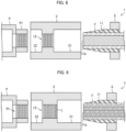
- FIG. 8 is a cross-sectional view illustrating a first mounting example of the optical transmission path 1.
- an end part of the optical waveguide 11 (optical fiber) is inserted into a ferrule F having a cylindrical shape.
- the ferrule F is made of, for example, zirconia.
- an end part on an end surface 11a side of the optical waveguide 11 may be processed to have a tapered shape as illustrated in Fig. 8 .
- the end part opposite to the end surface 11a side of the optical waveguide 11 may be provided with a flange part G.
- the optical modulation element group 12 is stored in an optical connector C.
- the optical connector C is provided with a recess C1 for storing an end part of the optical waveguide 11 together with the ferrule F and a recess C2 for storing a protrusion P1 of an optical processor P.
- the optical modulation element group 12 is provided in a space between the recess C1 and the recess C2.
- the present mounting example enables the optical processor P and the optical waveguide 11 to be easily connected with each other via the optical connector C.
- phase-modulation amounts of the cells of the optical modulation elements 121 to 124 are variable, it is possible to employ a configuration in which the phase-modulation amounts of the cells of the optical modulation elements 121 to 124 are set in accordance with the optical waveguide 11 to be connected. No matter what optical fiber the optical waveguide 11 is, this configuration makes it possible to appropriately compensate for a change in the two-dimensional intensity distribution of signal light which occurs in the optical fiber. For example, if a phase-modulation amount for an optical fiber having a length of one meter, a phase-modulation amount for an optical fiber having a length of two meters, ...
- the optical connector C may include a control part (not shown) configured to set the phase-modulation amounts of the cells of the optical modulation elements 121 to 124.
- a microlens array L may be added so as to follow the optical modulation element group 12. This makes it possible to more reliably guide, to the cores of the optical waveguide 11, signal light which has passed through the optical modulation element group 12.
- aspects of the present invention can also be expressed as follows:
- a configuration is employed of including: an optical waveguide; and an optical modulation element that has a plurality of cells having respective phase-modulation amounts set independently of each other and that has one main surface provided so as to face one end surface of the optical waveguide, wherein the respective phase-modulation amounts of the plurality of cells which constitute the optical modulation element are set so as to compensate for a change in two-dimensional intensity distribution of signal light, the change occurring in the optical waveguide.
- a configuration is employed in which the respective phase-modulation amounts of the plurality of cells which constitute the optical modulation element are set such that a difference between a two-dimensional intensity distribution of signal light which enters the other main surface of the optical modulation element and a two-dimensional intensity distribution of signal light which is emitted from the other end surface of the optical waveguide becomes smaller than in a case where the optical modulation element is absent.
- an antireflection film is formed on the one end surface of the optical waveguide.
- a configuration is employed in which the respective phase-modulation amounts of the plurality of cells which constitute the optical modulation element are set such that a difference between a two-dimensional intensity distribution of signal light which enters the other end surface of the optical waveguide and a two-dimensional intensity distribution of signal light which is emitted from the other main surface of the optical modulation element becomes smaller than in a case where the optical modulation element is absent.
- a configuration is employed of further including another optical modulation element that has a plurality of cells having respective phase-modulation amounts which are able to be set independently of each other and that has one main surface provided so as to face the other end surface of the optical waveguide.
- a configuration is employed in which the respective phase-modulation amounts of the plurality of cells which constitute the optical modulation element and the respective phase-modulation amounts of the plurality of cells which constitute the another optical modulation element are set such that a difference between a two-dimensional intensity distribution of signal light which enters the other main surface of the optical modulation element and a two-dimensional intensity distribution of signal light which is emitted from the other main surface of the another optical modulation element becomes smaller than in a case where the optical modulation element and the another optical modulation element are absent.
- Aspect 7 of the present invention in addition to the configuration of any one of Aspects 1 to 6, a configuration is employed in which the optical waveguide guides the signal light with use of a single core.
- an optical transmission path in accordance with Aspect 8 of the present invention in addition to the configuration of any one of Aspects 1 to 6, a configuration is employed in which the optical waveguide guides the signal light with use of a plurality of cores.
- a configuration is employed of including: an optical waveguide; an optical modulation element that has a plurality of cells having respective phase-modulation amounts which are able to be set independently of each other and that has one main surface provided so as to face one end surface of the optical waveguide; and a control part configured to set the respective phase-modulation amounts of the plurality of cells which constitute the optical modulation element so as to compensate for a change in two-dimensional intensity distribution of signal light, the change occurring in the optical waveguide.
- An optical connector in accordance with Aspect 10 of the present invention is an optical connector for connecting an optical waveguide and an optical processor, and in the optical connector, a configuration is employed of including: an optical modulation element that has a plurality of cells having respective phase-modulation amounts set independently of each other and that has one main surface provided so as to face one end surface of the optical waveguide, wherein the respective phase-modulation amounts of the plurality of cells which constitute the optical modulation element are set so as to compensate for a change in two-dimensional intensity distribution of signal light, the change occurring in the optical waveguide.
- Connecting the optical waveguide and the optical processor via the optical connector enables compensating for a change in the two-dimensional intensity distribution of signal light which occurs in the optical waveguide.
- An optical connector in accordance with Aspect 11 of the present invention is an optical connector for connecting an optical waveguide and an optical processor, and in the optical connector, a configuration is employed of including an optical modulation element that has a plurality of cells having respective phase-modulation amounts which are able to be set independently of each other and that has one main surface provided so as to face one end surface of the optical waveguide; and a control part configured to set the respective phase-modulation amounts of the plurality of cells which constitute the optical modulation element so as to compensate for a change in two-dimensional intensity distribution of signal light, the change occurring in the optical waveguide.
- Connecting the optical waveguide and the optical processor via the optical connector enables compensating for a change in the two-dimensional intensity distribution of signal light which occurs in the optical waveguide.
Landscapes
- Physics & Mathematics (AREA)
- Nonlinear Science (AREA)
- General Physics & Mathematics (AREA)
- Optics & Photonics (AREA)
- Optical Integrated Circuits (AREA)
Abstract
Description
- The present invention relates to an optical transmission path including an optical waveguide. In addition, the present invention relates to an optical connector for connecting an optical processor and an optical waveguide.
- Research and development on optical processors that optically perform computing are underway in order to surpass limits of electrical processors, such as a central processing unit (CPU) and a graphics processing unit (GPU), which electrically perform computing. Using such optical processors enables computing to be performed at higher speed than electrical processors. Examples of technologies contributing to achieving such optical processors include an optical transistor disclosed in Non-Patent Literature 1. Citation List
- [Non-patent Literature 1]
Nozaki, K., Matsuo, S., Fujii, T. et al. Femtofarad optoelectronic integration demonstrating energy-saving signal conversion and nonlinear functions. Nat. Photonics 13, 454-459 (2019). https://doi.org/10.1038/s41566-019-0397-3 - However, in a system including a plurality of optical processors, when these optical processors are connected via electrical transmission paths, a process of converting an optical signal into an electrical signal results in a bottleneck, and thus a computing speed as an entire system is not sufficiently improved.
- In particular, some optical processors output optical signals that express two-dimensional data, such as images, through two-dimensional intensity distributions. In a case where such an optical processor is connected via an electrical transmission path, it is required to (1) read two-dimensional data of m rows × n columns indicated by an optical signal, (2) generate m pieces of one-dimensional data corresponding to the rows of the two-dimensional data thus read, (3) generate m electrical signals indicating the respective m pieces of one-dimensional data thus generated, and (4) sequentially transmit the m electrical signals thus generated. Thus, no matter how fast the computing optically performed by the optical processors is, the high speed cannot be utilized. Therefore, such an optical processor is connected preferably via an optical transmission path, not via an electrical transmission path.
- Note, however, that in a case where an optical waveguide is used as the optical transmission path, an optical signal outputted from an optical processor cannot be transmitted with the two-dimensional intensity distribution thereof maintained. This is because the two-dimensional intensity distribution of an optical signal changes during a process of guiding the optical signal in an optical waveguide.
- An aspect of the present invention is achieved in light of the foregoing problem, and it is an object of the aspect to achieve an optical transmission path that enables compensating for a change in two-dimensional intensity distribution of signal light which occurs in an optical waveguide.
- In an optical transmission path in accordance with an aspect of the present invention, a configuration is employed of including: an optical waveguide; and an optical modulation element that has a plurality of cells having respective phase-modulation amounts set independently of each other and that has one main surface provided so as to face one end surface of the optical waveguide, wherein the respective phase-modulation amounts of the plurality of cells which constitute the optical modulation element are set so as to compensate for a change in two-dimensional intensity distribution of signal light, the change occurring in the optical waveguide.
- In an optical transmission path in accordance with another aspect of the present invention, a configuration is employed of including: an optical waveguide; an optical modulation element that has a plurality of cells having respective phase-modulation amounts which are able to be set independently of each other and that has one main surface provided so as to face one end surface of the optical waveguide; and a control part configured to set the respective phase-modulation amounts of the plurality of cells which constitute the optical modulation element so as to compensate for a change in two-dimensional intensity distribution of signal light, the change occurring in the optical waveguide.
- An optical connector in accordance with an aspect of the present invention is an optical connector for connecting an optical waveguide and an optical processor, and in the optical connector, a configuration is employed of including: an optical modulation element that has a plurality of cells having respective phase-modulation amounts set independently of each other and that has one main surface provided so as to face one end surface of the optical waveguide, wherein the respective phase-modulation amounts of the plurality of cells which constitute the optical modulation element are set so as to compensate for a change in two-dimensional intensity distribution of signal light, the change occurring in the optical waveguide.
- An optical connector in accordance with another aspect of the present invention is an optical connector for connecting an optical waveguide and an optical processor, and in the optical connector, a configuration is employed of including an optical modulation element that has a plurality of cells having respective phase-modulation amounts which are able to be set independently of each other and that has one main surface provided so as to face one end surface of the optical waveguide; and a control part configured to set the respective phase-modulation amounts of the plurality of cells which constitute the optical modulation element so as to compensate for a change in two-dimensional intensity distribution of signal light, the change occurring in the optical waveguide.
- According to an aspect of the present invention, it is possible to achieve an optical transmission path that enables compensating for a change in two-dimensional intensity distribution of signal light which occurs in an optical waveguide.
-
-
Fig. 1 is a perspective view illustrating a configuration of an optical transmission path in accordance with an embodiment of the present invention. -
Fig. 2 is a view illustrating a function of an optical modulation element group in the optical transmission path shown inFig. 1 . (a) ofFig. 2 illustrates a specific example of a two-dimensional intensity distribution of signal light which enters an optical modulation element, and (b), (c), and (d) ofFig. 2 each illustrate a specific example of a cross-sectional structure of an optical waveguide. - (a) of
Fig. 3 is a plan view illustrating a first specific example of an optical modulation element included in the optical transmission path shown inFig. 1 . (b) ofFig. 3 is an enlarged perspective view of a part of the optical modulation element. - (a) of
Fig. 4 is a plan view illustrating a second specific example of an optical modulation element included in the optical transmission path shown inFig. 1 . (b) ofFig. 4 is a cross-sectional view of a cell included in the optical modulation element. -
Fig. 5 is a perspective view illustrating a first variation of the optical transmission path shown inFig. 1 . -
Fig. 6 is a perspective view illustrating a second variation of the optical transmission path shown inFig. 1 . -
Fig. 7 is a perspective view illustrating a third variation of the optical transmission path shown inFig. 1 . -
Fig. 8 is a cross-sectional view illustrating a first mounting example of the optical transmission path shown inFig. 1 . -
Fig. 9 is a perspective view illustrating a second mounting example of the optical transmission path shown inFig. 1 . - With reference to
Fig. 1 , the following description will discuss a configuration of anoptical transmission path 1 in accordance with an embodiment of the present invention.Fig. 1 is a perspective view illustrating a configuration of theoptical transmission path 1. - The
optical transmission path 1 is a transmission path configured to transmit signal light. Theoptical transmission path 1 is used for, for example, connection between boards in which two optical processors mounted on different boards are connected or connection within a board in which two optical processors mounted on the same board are connected. As shown inFig. 1 , theoptical transmission path 1 includes anoptical waveguide 11 and an opticalmodulation element group 12. - The
optical waveguide 11 is a unit configured to guide signal light. As theoptical waveguide 11, for example, an optical fiber or a board-type optical waveguide (for example, silicon waveguide) can be used. In the present embodiment, as theoptical waveguide 11, an optical fiber is used. - The optical
modulation element group 12 is a unit configured to compensate for a change in two-dimensional intensity distribution of signal light which occurs during a process of guiding the signal light in theoptical waveguide 11. The opticalmodulation element group 12 is constituted by at least one optical modulation element. In the present embodiment, as the opticalmodulation element group 12, an optical modulation element group constituted by fouroptical modulation elements 121 to 124 is used. As described later, each of theoptical modulation elements 121 to 124 is constituted by a plurality of cells having respective phase-modulation amounts that can be set independently of each other. - The
optical modulation element 121 is provided in a manner such that onemain surface 121a thereof faces oneend surface 11a of theoptical waveguide 11. Theoptical modulation element 122 is provided between theoptical modulation element 121 and theoptical waveguide 11 as in the case of theoptical modulation element 121. Theoptical modulation element 123 is provided between theoptical modulation element 122 and theoptical waveguide 11 as in the case of theoptical modulation element 121. Theoptical modulation element 124 is provided between theoptical modulation element 123 and theoptical waveguide 11 as in the case of theoptical modulation element 121. Therefore, signal light Li to be inputted from an optical processor into theoptical transmission path 1 passes through theoptical modulation element 121, theoptical modulation element 122, theoptical modulation element 123, and theoptical modulation element 124 in this order and then is inputted from theend surface 11a into theoptical waveguide 11. - The respective phase-modulation amounts of the cells of the
optical modulation elements 121 to 124 are set so as to compensate for a change in two-dimensional intensity distribution of signal light which occurs during a process of guiding the signal light in theoptical waveguide 11. In other words, the phase-modulation amounts are set such that a difference between the two-dimensional intensity distribution of the signal light Li which enters the othermain surface 121b of theoptical modulation element 121 and the two-dimensional intensity distribution of signal light Lo which is emitted from theother end surface 11b of theoptical waveguide 11 becomes smaller than in a case where the opticalmodulation element group 12 is absent. - It is possible to achieve setting of the phase-modulation amounts of the cells of the
optical modulation elements 121 to 124, for example, through machine learning. In this machine learning, it is possible to use, for example, a model in which a two-dimensional intensity distribution of the signal light Li which enters themain surface 121b of theoptical modulation element 121 is an input and a two-dimensional intensity distribution of the signal light Lo which is emitted from theend surface 11b of theoptical waveguide 11 is an output and which includes a phase-modulation amount of each of the cells of theoptical modulation elements 121 to 124 as a parameter. It is possible to suitably set the phase-modulation amounts of the cells of theoptical modulation elements 121 to 124 by repeating a process of updating the parameter of the model for various signal light (training data) so as to diminish a difference between the input and the output of the model. - On the
end surface 11a of theoptical waveguide 11, an antireflection film AR may be formed. This makes it possible to reduce a risk that signal light that has been emitted from the opticalmodulation element group 12 is reflected by theend surface 11a of theoptical waveguide 11 and enters the opticalmodulation element group 12 again. - In a case where the phase-modulation amounts of the cells of the
optical modulation elements 121 to 124 are variable, theoptical transmission path 1 preferably includes a control part (not shown) configured to set the phase-modulation amounts of the cells of theoptical modulation elements 121 to 124 as described above. - Although, in the present embodiment, all of the
optical modulation elements 121 to 124 are used for the compensation described above, this should not be construed as a limitation. For example, it is possible that some of theoptical modulation elements 121 to 124 are used for the compensation described above and the other optical modulation elements are used for another optical computing. In this case, an optical waveguide having an optical computing function is achieved. - The
optical modulation elements 121 to 124 may be integrated together. For example, four light diffraction layers formed inside a structure that allows signal light to pass therethrough, such as a dried gel may be used as theoptical modulation elements 121 to 124. In this case, it is preferable to use a gel that is subjected to dehydration shrinkage so that the gel shrinks while keeping a similar shape, e.g., a gel used in the Implosion Fabrication process. This makes it possible to, by drying a swollen gel in which four light diffraction layers are formed, easily manufacture the opticalmodulation element group 12 in which theoptical modulation elements 121 to 124 are accurately arranged. - With reference to
Fig. 2 , the following description will discuss the function of the opticalmodulation element group 12 in theoptical transmission path 1. (a) ofFig. 2 indicates a specific example of the two-dimensional intensity distribution of the signal light Li which enters theoptical modulation element 121, and (b), (c), and (d) ofFig. 2 each indicate a specific example of a cross-sectional structure of theoptical waveguide 11. Here, it is assumed that the two-dimensional intensity distribution of the signal light L1 has a cell structure of 4 × 4, as shown in (a) ofFig. 2 . - In the specific example shown in (b) of
Fig. 2 , theoptical waveguide 11 has onecore 111 having a cross-sectional area substantially equal to a beam cross-sectional area of the signal light Li. In this case, the entire signal light Li is coupled to thecore 111 of theoptical waveguide 11. Therefore, the two-dimensional intensity distribution of the signal light Li changes mainly by the signal light Li being guided in thecore 111. One example of causes of the change is the following situation: the beams of the signal light Li which have been emitted from the cells of theoptical modulation element 124 and are propagating inside thecore 111 while dispersing interfere with each other and are totally reflected on an interface between the core 111 and a clad 112, so that the two-dimensional intensity distribution becomes out of shape. The phase-modulation amounts of the cells of theoptical modulation elements 121 to 124 are set so as to compensate for this change. Therefore, the two-dimensional intensity distribution of the signal light Lo which is outputted from theend surface 11b of theoptical waveguide 11 becomes closer to the two-dimensional intensity distribution of the signal light Li which is inputted into themain surface 121b of theoptical modulation element 121 than in a case where the opticalmodulation element group 12 is absent. - In the specific example shown in (c) of
Fig. 2 , theoptical waveguide 11 has 16cores 111 each having a cross-sectional area approximately one sixteenth the beam cross-sectional area of the signal light Li. In this case, the signal light Li for one cell is coupled to each of thecores 111 of theoptical waveguide 11. Therefore, the two-dimensional intensity distribution of the signal light Li changes mainly due to crosstalk occurring betweenadjacent cores 111. The phase-modulation amounts of the cells of theoptical modulation elements 121 to 124 are set so as to compensate for this change. Therefore, the two-dimensional intensity distribution of the signal light Lo which is outputted from theend surface 11b of theoptical waveguide 11 becomes closer to the two-dimensional intensity distribution of the signal light Li which is inputted into themain surface 121b of theoptical modulation element 121 than in a case where the opticalmodulation element group 12 is absent. - In the specific example shown in (d) of
Fig. 2 , theoptical waveguide 11 has fourcores 111 each having a cross-sectional area approximately one fourth the beam cross-sectional area of the signal light Li. In this case, the signal light Li for four cells is coupled to each of thecores 111 of theoptical waveguide 11. Therefore, the two-dimensional intensity distribution of the signal light Li is subject mainly to a change caused by the signal light Li being guided in each of thecores 111 and a change caused by cross talk occurring betweenadjacent cores 111. The phase-modulation amounts of the cells of theoptical modulation elements 121 to 124 are set so as to compensate for these changes. Therefore, the two-dimensional intensity distribution of the signal light Lo which is outputted from theend surface 11b of theoptical waveguide 11 becomes closer to the two-dimensional intensity distribution of the signal light Li which is inputted into themain surface 121b of theoptical modulation element 121 than in a case where the opticalmodulation element group 12 is absent. - The following description will discuss, with reference to
Fig. 3 , a first specific example of theoptical modulation elements 121 to 124. Here, theoptical modulation element 121 is taken as an example, but theoptical modulation elements 122 to 124 are configured as in the case of theoptical modulation element 121. (a) ofFig. 3 is a plan view of theoptical modulation element 121 in accordance with the present specific example. (b) ofFig. 3 is an enlarged perspective view of a part (i.e., a part surrounded by the broken lines in (a) ofFig. 3 ) of theoptical modulation element 121 in accordance with the present specific example. - As shown in (a) of
Fig. 3 , theoptical modulation element 121 is constituted by a plurality of microcells C having respective phase-modulation amounts that are set independently of each other. When signal light enters theoptical modulation element 121, the signal light is phase-modulated by the microcells C, and signal light beams thus phase-modulated by the respective microcells C interfere with each other. Consequently, predetermined optical computing (conversion of a two-dimensional intensity distribution according to a predetermined conversion rule) is carried out. The phase-modulation amounts of the microcells C may be variable or may be fixed. In the present specific example, the phase-modulation amounts are fixed. - In the present specification, the "microcell" means a cell having a cell size of less than 10 µm, for example. Further, the "cell size" means a square root of an area of a cell. For example, given that the microcell C is in the form of a square in a plan view, a cell size of the microcell C means a length of one side of the microcell C. A lower limit of the cell size of the microcell C is 1 nm, for example.
- The
optical modulation element 121 shown in (a) ofFig. 3 as an example is constituted by 200 × 200 microcells C arranged in a matrix. A shape of each microcell C in a plan view is a square of 500 nm × 500 nm. A shape of theoptical modulation element 121 in a plan view is a square of 100 µm × 100 µm. - A phase-modulation amount of each microcell C can be set independently for the cell by (1) setting a thickness of the microcell C independently for the cell or (2) selecting a refractive index of the microcell C independently for the cell. The present specific example employs the method (1), which can be carried out by nanoimprinting. In this case, as shown in (b) of
Fig. 3 , each microcell C is constituted by a pillar having a quadrangular prism shape having a square bottom surface with sides each having a length equal to a cell size. In this case, the phase-modulation amount of the signal light passing through each microcell C is determined in accordance with a height of a pillar constituting the microcell C. That is, a microcell C constituted by a pillar having a high height has a large phase-modulation amount, whereas a microcell C constituted by a pillar having a low height has a small phase-modulation amount. - The following description will discuss, with reference to
Fig 4 , a second specific example of theoptical modulation elements 121 to 124. Here, theoptical modulation element 121 is taken as an example, but theoptical modulation elements 122 to 124 are configured as in the case of theoptical modulation element 121. (a) ofFig. 4 is a plan view of theoptical modulation element 121 in accordance with the present specific example. (b) ofFig. 4 is a cross-sectional view of a cell C included in theoptical modulation element 121 in accordance with the present specific example. - As shown in (a) of
Fig. 4 , theoptical modulation element 121 is constituted by a plurality of microcells C having respective phase-modulation amounts that are set independently of each other. When signal light enters theoptical modulation element 121, the signal light is phase-modulated by the microcells C, and signal light beams thus phase-modulated by the respective microcells C interfere with each other. Consequently, the predetermined optical computing is carried out. The phase-modulation amounts of the microcells C may be variable or may be fixed. In the present specific example, the phase-modulation amounts are variable. - The
optical modulation element 121 shown in (a) ofFig. 4 as an example is constituted by 200 × 200 microcells C arranged in a matrix. A shape of each microcell C in a plan view is a square of 500 nm × 500 nm. A shape of theoptical modulation element 121 in a plan view is a square of 100 µm × 100 µm. - For example, as shown in (b) of
Fig. 4 , each microcell C constituting theoptical modulation element 121 may be constituted by a first polarizing plate C11, a second polarizing plate C12, a first electrode C13, a magnetization free layer C14, an insulating layer C15, a magnetization fixed layer C16, and a second electrode C17. - The first polarizing plate C11 and the second polarizing plate C12 are provided so as to face each other. The first electrode C13, the magnetization free layer C14, the insulating layer C15, the magnetization fixed layer C16, and the second electrode C17 are stacked in this order, and are sandwiched between the first polarizing plate C11 and the second polarizing plate C12. Here, a direction in which the first electrode C13, the magnetization free layer C14, the insulating layer C15, the magnetization fixed layer C16, and the second electrode C17 are stacked is orthogonal to a direction in which the first polarizing plate C11 and the second polarizing plate C12 are stacked. Thus, a first side surface of the magnetization free layer C14 is in surface contact with the first polarizing plate C11, and a second side surface of the magnetization free layer C14 which faces the first side surface is in surface contact with the second polarizing plate C12. The signal light L (1) enters an inside of the magnetization free layer C14 via the first polarizing plate C11, (2) propagates inside the magnetization free layer C14, and (3) is emitted through the second polarizing plate C12 to an outside of the magnetization free layer C14.
- The magnetization free layer C14 is made of, for example, a soft magnetic material having electric conductivity and light transmissivity (for example, CoFeB). The magnetization fixed layer C16 is made of, for example, a hard magnetic material having electric conductivity (for example, permalloy). Selected as the first polarizing plate C11 and the second polarizing plate C12 is a polarizing plate that selectively allows, to pass therethrough, a polarized light component having a polarization direction P parallel to a magnetization direction M of the magnetization fixed layer C16. (b) of
Fig. 4 takes as an example a case in which the magnetization direction M and the polarization direction P are parallel to both a main surface of the first polarizing plate C11 and a main surface of the magnetization fixed layer C16. - When a potential difference is provided between the first electrode C13 and the second electrode C17, a tunnel effect occurs and injects a spin current (a flow of spin-polarized electrons) from the magnetization fixed layer C16 through the insulating layer C15 into the magnetization free layer C14 to magnetize the magnetization free layer C14. Here, the magnetization occurring in the magnetization free layer C14 is magnetization parallel to the magnetization direction M of the magnetization fixed layer C16, that is, magnetization parallel to the polarization direction P of the signal light entering the magnetization free layer C14 through the first polarizing plate C11. This causes a phase of the signal light to be delayed by a transverse Kerr effect during a process of propagation in the magnetization free layer C14.
- Here, a phase-shift amount of the signal light in the cell C is determined depending on a magnitude of the magnetization in the magnetization free layer C14. The magnitude of the magnetization in the magnetization free layer C14 is determined depending on a magnitude of the spin current injected into the magnetization free layer C14. The magnitude of the spin current injected into the magnetization free layer C14 is determined depending on the potential difference provided between the first electrode C13 and the second electrode C17. Thus, controlling the potential difference provided between the first electrode C13 and the second electrode C17 enables the phase-modulation amount of the cell C to be controlled (to be set to a desired value).
- The present specific example describes a cell C having a configuration similar to that of a spin transfer torque (STT)-magnetoresistive random access memory (MRAM). However, this should not be construed as a limitation. For example, a cell C having a configuration similar to a spin orbit torque (SOT)-MRAM may be used. Note that such a cell C can be achieved by, for example, removing the insulating layer C15, the magnetization fixed layer C16, and the second electrode C17 from the structure shown in (b) of
Fig. 4 . In this case, for example, causing the first electrode C13 to contain heavy metal and providing a pulse voltage or a pulse current to the first electrode C13 enable the spin current to be efficiently injected into the magnetization free layer C14. - With reference to
Fig. 5 , the following description will discuss a first variation of the optical transmission path 1 (hereinafter, referred to as an "optical transmission path 1A").Fig. 5 is a perspective view illustrating a configuration of theoptical transmission path 1A. - The
optical transmission path 1A differs from theoptical transmission path 1 in a direction in which signal light is expected to be transmitted. That is, in theoptical transmission path 1, proceeding signal light entering themain surface 121b of theoptical modulation element 121 expected, whereas in theoptical transmission path 1A, receding signal light entering theend surface 11b of theoptical waveguide 11 is expected. - Therefore, in the
optical transmission path 1A, the phase-modulation amounts of the cells of theoptical modulation elements 121 to 124 are set such that a difference between the intensity distribution of the signal light Li which enters theend surface 11b of theoptical waveguide 11 and the intensity distribution of the signal light Lo which is emitted from themain surface 121b of theoptical modulation element 121 becomes smaller than in a case where the opticalmodulation element group 12 is absent. This enables post-compensation for a change in the two-dimensional intensity distribution of the receding signal light which occurs in theoptical waveguide 11. - With reference to
Fig. 6 , the following description will discuss a second variation of the optical transmission path 1 (hereinafter, referred to as an "optical transmission path 1B").Fig. 6 is a perspective view illustrating a configuration of theoptical transmission path 1B. - The
optical transmission path 1B differs from theoptical transmission path 1 in a direction in which signal light is expected to be transmitted. That is, in theoptical transmission path 1B, both the proceeding signal light entering themain surface 121b of theoptical modulation element 121 and the receding signal light entering theend surface 11b of theoptical waveguide 11 are expected. - Therefore, in the
optical transmission path 1B, the phase-modulation amounts of the cells of theoptical modulation elements 121 to 124 are set such that (1) a difference between the two-dimensional intensity distribution of signal light L1i which enters themain surface 121b of theoptical modulation element 121 and the two-dimensional intensity distribution of signal light L1o which is emitted from theend surface 11b of theoptical waveguide 11 becomes smaller than in a case where the opticalmodulation element group 12 is absent, and (2) a difference between the two-dimensional intensity distribution of signal light L2i which enters theend surface 11b of theoptical waveguide 11 and the two-dimensional intensity distribution of the signal light L2o which is emitted from themain surface 121b of theoptical modulation element 121 becomes smaller than in a case where the opticalmodulation element group 12 is absent. This enables both pre-compensation for a change in the two-dimensional intensity distribution of the proceeding signal light which occurs in theoptical waveguide 11 and post-compensation for a change in the two-dimensional intensity distribution of the receding signal light which occurs in theoptical waveguide 11. - Note that it is preferable that the proceeding signal light which enters the
main surface 121b of theoptical modulation element 121 and the receding signal light which enters theend surface 11b of theoptical waveguide 11 have different polarization directions. This makes it easy to set the phase-modulation amounts of the cells of theoptical modulation elements 121 to 124 so as to satisfy both the conditions (1) and (2) described above. - Further, it is preferable that the antireflection film AR is formed on the
end surface 11a of theoptical waveguide 11. This makes it possible to reduce a risk that signal light that has been emitted from the opticalmodulation element group 12 is reflected by theend surface 11a of theoptical waveguide 11 and enters the opticalmodulation element group 12 again. - With reference to
Fig. 7 , the following description will discuss a third variation of the optical transmission path 1 (hereinafter, referred to as an "optical transmission path 1C").Fig. 7 is a perspective view illustrating a configuration of the optical transmission path 1C. - The optical transmission path 1C differs from the
optical transmission path 1 in that an opticalmodulation element group 13 is added. As in the case of the opticalmodulation element group 12, the opticalmodulation element group 13 is a unit configured to compensate for a change in the two-dimensional intensity distribution of signal light which occurs during a process of guiding the signal light in theoptical waveguide 11 and is constituted by at least one optical modulation element. In the present variation, as the opticalmodulation element group 13, an optical modulation element group constituted by fouroptical modulation elements 131 to 134 is used. As in the case of theoptical modulation elements 121 to 124, theoptical modulation elements 131 to 134 are each constituted by a plurality of cells having respective phase-modulation amounts that can be set independently of each other. - The phase-modulation amounts of the cells of the
optical modulation elements 121 to 124 and theoptical modulation elements 131 to 134 are set such that a difference between the two-dimensional intensity distribution of the signal light Li which enters themain surface 121b of theoptical modulation element 121 and the two-dimensional intensity distribution of the signal light Li which is emitted from anend surface 131b of theoptical modulation element 131 becomes smaller than in a case where the opticalmodulation element group 12 and the opticalmodulation element group 13 are absent. This enables pre- and post-compensation for a change in the two-dimensional intensity distribution of the proceeding signal light which occurs in theoptical waveguide 11. - In this case, it is preferable that the antireflection film AR is formed on the
end surface 11a of theoptical waveguide 11. This makes it possible to reduce a risk that signal light that has been emitted from the opticalmodulation element group 12 is reflected by theend surface 11a of theoptical waveguide 11 and enters the opticalmodulation element group 12 again. - Note that the phase-modulation amounts of the cells of the
optical modulation elements 121 to 124 and theoptical modulation elements 131 to 134 may be set such that (1) a difference between the two-dimensional intensity distribution of the signal light Li which enters themain surface 121b of theoptical modulation element 121 and the two-dimensional intensity distribution of the signal light Li which is emitted from theend surface 131b of theoptical modulation element 131 becomes smaller than in a case where the opticalmodulation element group 12 and the opticalmodulation element group 13 are absent, and (2) a difference between the two-dimensional intensity distribution of signal light (not shown) which enters theend surface 131b of theoptical modulation element 131 and the two-dimensional intensity distribution of signal light (not shown) which is emitted from themain surface 121b of theoptical modulation element 121 becomes smaller than in a case where the opticalmodulation element group 12 and the opticalmodulation element group 13 are absent. This enables pre- and post-compensation for a change in the two-dimensional intensity distribution of the proceeding signal light which occurs in theoptical waveguide 11 and pre- and post-compensation for a change in the two-dimensional intensity distribution of the receding signal light which occurs in theoptical waveguide 11. - In this case, it is preferable that also on the
end surface 11b of theoptical waveguide 11, an antireflection film (not shown) is formed. This makes it possible to reduce a risk that signal light that has been emitted from the opticalmodulation element group 13 is reflected by theend surface 11b of theoptical waveguide 11 and enters the opticalmodulation element group 13 again. - Note that although in the present variation, both the optical
modulation element group 12 and the opticalmodulation element group 13 are used for the compensation described above, this should not be construed as a limitation. For example, it is possible that the opticalmodulation element group 12 is used for the compensation described above and the opticalmodulation element group 13 is used for another optical computing. In this case, an optical waveguide having an optical computing function is achieved. - With reference to
Fig. 8 , the following description will discuss an example in which theoptical transmission path 1 is mounted.Fig. 8 is a cross-sectional view illustrating a first mounting example of theoptical transmission path 1. - In the present mounting example, an end part of the optical waveguide 11 (optical fiber) is inserted into a ferrule F having a cylindrical shape. The ferrule F is made of, for example, zirconia. Among the end parts of the ferrule F, an end part on an
end surface 11a side of theoptical waveguide 11 may be processed to have a tapered shape as illustrated inFig. 8 . Further, among the end parts of the ferrule F, the end part opposite to theend surface 11a side of theoptical waveguide 11 may be provided with a flange part G. - In the present mounting example, the optical
modulation element group 12 is stored in an optical connector C. The optical connector C is provided with a recess C1 for storing an end part of theoptical waveguide 11 together with the ferrule F and a recess C2 for storing a protrusion P1 of an optical processor P. The opticalmodulation element group 12 is provided in a space between the recess C1 and the recess C2. - The present mounting example enables the optical processor P and the
optical waveguide 11 to be easily connected with each other via the optical connector C. - In a case where the phase-modulation amounts of the cells of the
optical modulation elements 121 to 124 are variable, it is possible to employ a configuration in which the phase-modulation amounts of the cells of theoptical modulation elements 121 to 124 are set in accordance with theoptical waveguide 11 to be connected. No matter what optical fiber theoptical waveguide 11 is, this configuration makes it possible to appropriately compensate for a change in the two-dimensional intensity distribution of signal light which occurs in the optical fiber. For example, if a phase-modulation amount for an optical fiber having a length of one meter, a phase-modulation amount for an optical fiber having a length of two meters, ... are prepared in advance, no matter how long optical fiber theoptical waveguide 11 is, it is possible to appropriately compensate for a change in the two-dimensional intensity distribution of signal light which occurs in the optical fiber. In this case, the optical connector C may include a control part (not shown) configured to set the phase-modulation amounts of the cells of theoptical modulation elements 121 to 124. - Further, as shown in
Fig. 9 , a microlens array L may be added so as to follow the opticalmodulation element group 12. This makes it possible to more reliably guide, to the cores of theoptical waveguide 11, signal light which has passed through the opticalmodulation element group 12. - Aspects of the present invention can also be expressed as follows:
In an optical transmission path in accordance withAspect 1 of the present invention, a configuration is employed of including: an optical waveguide; and an optical modulation element that has a plurality of cells having respective phase-modulation amounts set independently of each other and that has one main surface provided so as to face one end surface of the optical waveguide, wherein the respective phase-modulation amounts of the plurality of cells which constitute the optical modulation element are set so as to compensate for a change in two-dimensional intensity distribution of signal light, the change occurring in the optical waveguide. - According to the above configuration, it is possible to achieve an optical transmission path that enables compensating for a change in two-dimensional intensity distribution of signal light which occurs in an optical waveguide.
- In an optical transmission path in accordance with Aspect 2 of the present invention, in addition to the configuration of
Aspect 1, a configuration is employed in which the respective phase-modulation amounts of the plurality of cells which constitute the optical modulation element are set such that a difference between a two-dimensional intensity distribution of signal light which enters the other main surface of the optical modulation element and a two-dimensional intensity distribution of signal light which is emitted from the other end surface of the optical waveguide becomes smaller than in a case where the optical modulation element is absent. - According to the above configuration, it is possible to achieve an optical transmission path that, with respect to signal light which enters the other main surface of the optical modulation element, enables compensating for a change in two-dimensional intensity distribution which occurs in an optical waveguide.
- In an optical transmission path in accordance with Aspect 3 of the present invention, in addition to the configuration of
Aspect 1 or 2, a configuration is employed in which an antireflection film is formed on the one end surface of the optical waveguide. - According to the above configuration, it is possible to reduce a risk that signal light that has been emitted from the optical modulation element is reflected by the end surface of the optical waveguide and enters the optical modulation element again.
- In an optical transmission path in accordance with
Aspect 4 of the present invention, in addition to the configuration of any one ofAspects 1 to 3, a configuration is employed in which the respective phase-modulation amounts of the plurality of cells which constitute the optical modulation element are set such that a difference between a two-dimensional intensity distribution of signal light which enters the other end surface of the optical waveguide and a two-dimensional intensity distribution of signal light which is emitted from the other main surface of the optical modulation element becomes smaller than in a case where the optical modulation element is absent. - According to the above configuration, it is possible to achieve an optical transmission path that, with respect to signal light which enters the other end surface of the optical waveguide, enables compensating for a change in two-dimensional intensity distribution which occurs in the optical waveguide.
- In an optical transmission path in accordance with Aspect 5 of the present invention, in addition to the configuration of
Aspect 1, a configuration is employed of further including another optical modulation element that has a plurality of cells having respective phase-modulation amounts which are able to be set independently of each other and that has one main surface provided so as to face the other end surface of the optical waveguide. - According to the above configuration, it is possible to achieve an optical transmission path in which both the optical modulation element and the another optical modulation element are used for compensating for a change in the two-dimensional intensity distribution of signal light which occurs in the optical waveguide, to enable the compensation to be performed more accurately. In addition, it is also possible to achieve an optical transmission path in which the optical modulation element is used for compensating for a change in the two-dimensional intensity distribution of signal light which occurs in the optical waveguide and the another optical modulation element is used for certain optical computing, to enable the optical computing to be performed in addition to the compensation.
- In an optical transmission path in accordance with Aspect 6 of the present invention, in addition to the configuration in accordance with Aspect 5, a configuration is employed in which the respective phase-modulation amounts of the plurality of cells which constitute the optical modulation element and the respective phase-modulation amounts of the plurality of cells which constitute the another optical modulation element are set such that a difference between a two-dimensional intensity distribution of signal light which enters the other main surface of the optical modulation element and a two-dimensional intensity distribution of signal light which is emitted from the other main surface of the another optical modulation element becomes smaller than in a case where the optical modulation element and the another optical modulation element are absent.
- According to the above configuration, it is possible to achieve an optical transmission path that, with respect to signal light which enters the other main surface of the optical modulation element, enables more accurately compensating for a change in two-dimensional intensity distribution which occurs in an optical waveguide.
- In an optical transmission path in accordance with Aspect 7 of the present invention, in addition to the configuration of any one of
Aspects 1 to 6, a configuration is employed in which the optical waveguide guides the signal light with use of a single core. - According to the above configuration, it is possible to achieve an optical transmission path that enables compensating for a change in the two-dimensional intensity distribution of signal light which occurs through the total reflection on a core-clad interface in the optical waveguide.
- In an optical transmission path in accordance with Aspect 8 of the present invention, in addition to the configuration of any one of
Aspects 1 to 6, a configuration is employed in which the optical waveguide guides the signal light with use of a plurality of cores. - According to the above configuration, it is possible to achieve an optical transmission path that enables compensating for a change in the two-dimensional intensity distribution of signal light which occurs through crosstalk between adjacent cores in the optical waveguide.
- In an optical transmission path in accordance with Aspect 9 of the present invention, a configuration is employed of including: an optical waveguide; an optical modulation element that has a plurality of cells having respective phase-modulation amounts which are able to be set independently of each other and that has one main surface provided so as to face one end surface of the optical waveguide; and a control part configured to set the respective phase-modulation amounts of the plurality of cells which constitute the optical modulation element so as to compensate for a change in two-dimensional intensity distribution of signal light, the change occurring in the optical waveguide.
- According to the above configuration, it is possible to achieve an optical transmission path that enables compensating for a change in two-dimensional intensity distribution of signal light which occurs in an optical waveguide.
- An optical connector in accordance with Aspect 10 of the present invention is an optical connector for connecting an optical waveguide and an optical processor, and in the optical connector, a configuration is employed of including: an optical modulation element that has a plurality of cells having respective phase-modulation amounts set independently of each other and that has one main surface provided so as to face one end surface of the optical waveguide, wherein the respective phase-modulation amounts of the plurality of cells which constitute the optical modulation element are set so as to compensate for a change in two-dimensional intensity distribution of signal light, the change occurring in the optical waveguide.
- Connecting the optical waveguide and the optical processor via the optical connector enables compensating for a change in the two-dimensional intensity distribution of signal light which occurs in the optical waveguide.
- An optical connector in accordance with
Aspect 11 of the present invention is an optical connector for connecting an optical waveguide and an optical processor, and in the optical connector, a configuration is employed of including an optical modulation element that has a plurality of cells having respective phase-modulation amounts which are able to be set independently of each other and that has one main surface provided so as to face one end surface of the optical waveguide; and a control part configured to set the respective phase-modulation amounts of the plurality of cells which constitute the optical modulation element so as to compensate for a change in two-dimensional intensity distribution of signal light, the change occurring in the optical waveguide. - Connecting the optical waveguide and the optical processor via the optical connector enables compensating for a change in the two-dimensional intensity distribution of signal light which occurs in the optical waveguide.
- The present invention is not limited to the description of the embodiments, but can be altered in many ways by a person skilled in the art within the scope of the claims. An embodiment derived from a proper combination of technical means disclosed in different embodiments is also encompassed in the technical scope of the present invention.
-
- 1
- Optical transmission path
- 11
- Optical waveguide
- 12
- Optical modulation element group
- 121 to 124
- Optical modulation element
- 13
- Optical modulation element group
- 131 to 134
- Optical modulation element
- P
- Optical processor
- C
- Optical connector
Claims (11)
- An optical transmission path comprising:an optical waveguide; andan optical modulation element that has a plurality of cells having respective phase-modulation amounts set independently of each other and that has one main surface provided so as to face one end surface of the optical waveguide, whereinthe respective phase-modulation amounts of the plurality of cells which constitute the optical modulation element are set so as to compensate for a change in two-dimensional intensity distribution of signal light, the change occurring in the optical waveguide.
- The optical transmission path according to claim 1, wherein the respective phase-modulation amounts of the plurality of cells which constitute the optical modulation element are set such that a difference between a two-dimensional intensity distribution of signal light which enters the other main surface of the optical modulation element and a two-dimensional intensity distribution of signal light which is emitted from the other end surface of the optical waveguide becomes smaller than in a case where the optical modulation element is absent.
- The optical transmission path according to claim 1 or 2, wherein an antireflection film is formed on the one end surface of the optical waveguide.
- The optical transmission path according to any one of claims 1 to 3, wherein the respective phase-modulation amounts of the plurality of cells which constitute the optical modulation element are set such that a difference between a two-dimensional intensity distribution of signal light which enters the other end surface of the optical waveguide and a two-dimensional intensity distribution of signal light which is emitted from the other main surface of the optical modulation element becomes smaller than in a case where the optical modulation element is absent.
- The optical transmission path according to claim 1, further comprising another optical modulation element that has a plurality of cells having respective phase-modulation amounts which are able to be set independently of each other and that has one main surface provided so as to face the other end surface of the optical waveguide.
- The optical transmission path according to claim 5, wherein the respective phase-modulation amounts of the plurality of cells which constitute the optical modulation element and the respective phase-modulation amounts of the plurality of cells which constitute the another optical modulation element are set such that a difference between a two-dimensional intensity distribution of signal light which enters the other main surface of the optical modulation element and a two-dimensional intensity distribution of signal light which is emitted from the other main surface of the another optical modulation element becomes smaller than in a case where the optical modulation element and the another optical modulation element are absent.
- The optical transmission path according to any one of claims 1 to 6, wherein the optical waveguide guides the signal light with use of a single core.
- The optical transmission path according to any one of claims 1 to 6, wherein the optical waveguide guides the signal light with use of a plurality of cores.
- An optical transmission path comprising:an optical waveguide;an optical modulation element that has a plurality of cells having respective phase-modulation amounts which are able to be set independently of each other and that has one main surface provided so as to face one end surface of the optical waveguide; anda control part configured to set the respective phase-modulation amounts of the plurality of cells which constitute the optical modulation element so as to compensate for a change in two-dimensional intensity distribution of signal light, the change occurring in the optical waveguide.
- An optical connector for connecting an optical waveguide and an optical processor, the optical connector comprising:an optical modulation element that has a plurality of cells having respective phase-modulation amounts set independently of each other and that has one main surface provided so as to face one end surface of the optical waveguide, whereinthe respective phase-modulation amounts of the plurality of cells which constitute the optical modulation element are set so as to compensate for a change in two-dimensional intensity distribution of signal light, the change occurring in the optical waveguide.
- An optical connector for connecting an optical waveguide and an optical processor, the optical connector comprising:an optical modulation element that has a plurality of cells having respective phase-modulation amounts which are able to be set independently of each other and that has one main surface provided so as to face one end surface of the optical waveguide; anda control part configured to set the respective phase-modulation amounts of the plurality of cells which constitute the optical modulation element so as to compensate for a change in two-dimensional intensity distribution of signal light, the change occurring in the optical waveguide.
Applications Claiming Priority (2)
| Application Number | Priority Date | Filing Date | Title |
|---|---|---|---|
| JP2022013190 | 2022-01-31 | ||
| PCT/JP2022/042726 WO2023145206A1 (en) | 2022-01-31 | 2022-11-17 | Optical transmission path and optical connector |
Publications (2)
| Publication Number | Publication Date |
|---|---|
| EP4474891A1 true EP4474891A1 (en) | 2024-12-11 |
| EP4474891A4 EP4474891A4 (en) | 2026-04-29 |
Family
ID=87471394
Family Applications (1)
| Application Number | Title | Priority Date | Filing Date |
|---|---|---|---|
| EP22924058.5A Pending EP4474891A4 (en) | 2022-01-31 | 2022-11-17 | OPTICAL TRANSMISSION PATH AND OPTICAL CONNECTOR |
Country Status (4)
| Country | Link |
|---|---|
| EP (1) | EP4474891A4 (en) |
| JP (1) | JP7829600B2 (en) |
| CN (1) | CN118414570A (en) |
| WO (1) | WO2023145206A1 (en) |
Families Citing this family (7)
| Publication number | Priority date | Publication date | Assignee | Title |
|---|---|---|---|---|
| EP4451044A1 (en) | 2023-04-20 | 2024-10-23 | Black Semiconductor GmbH | Device for modulating electromagnatic waves and method for producing the same |
| EP4516736A1 (en) | 2023-09-01 | 2025-03-05 | Black Semiconductor GmbH | Layered structure and method for the production of graphene |
| EP4531115A1 (en) | 2023-09-27 | 2025-04-02 | Black Semiconductor GmbH | Opto-electronic component with an electrical via connecting to an electrical conductor layer through two dielectric layers |
| EP4530709A1 (en) | 2023-09-27 | 2025-04-02 | Black Semiconductor GmbH | Method for producing planarized surfaces in layered structures used for producing opto-electronic devices |
| WO2025191953A1 (en) * | 2024-03-12 | 2025-09-18 | 株式会社フジクラ | Optical modulation device, optical integrated circuit, and optical arithmetic device |
| WO2026082598A1 (en) | 2024-10-15 | 2026-04-23 | Black Semiconductor Gmbh | Waveguide with recess for opto-electronic devices and coupled waveguides and method for producing the same |
| EP4729999A1 (en) | 2024-10-15 | 2026-04-22 | Black Semiconductor GmbH | Waveguide with recess for opto-electronic devices and coupled waveguides and method for producing the same |
Family Cites Families (9)
| Publication number | Priority date | Publication date | Assignee | Title |
|---|---|---|---|---|
| JP3399832B2 (en) * | 1998-04-20 | 2003-04-21 | シャープ株式会社 | Two-way optical communication device and two-way optical communication device |
| JP5081777B2 (en) * | 2008-09-24 | 2012-11-28 | 株式会社フジクラ | Mach-Zehnder interferometer type optical functional element |
| US8822905B2 (en) * | 2011-09-16 | 2014-09-02 | Alcatel Lucent | Optical mode couplers for multi-mode optical fibers |
| JP2017219560A (en) * | 2016-06-02 | 2017-12-14 | 日本電信電話株式会社 | Light beam control device |
| GB2551483B (en) * | 2016-06-13 | 2020-05-27 | Toshiba Res Europe Limited | A photon detection device and a method of manufacturing a photon detection device |
| EP3590207A4 (en) * | 2017-03-01 | 2021-01-06 | Corning Incorporated | QUANTUM COMMUNICATION SYSTEMS WITH DISPERSION-COMPENSATING OPTICAL FIBER CONNECTIONS |
| US10401883B2 (en) * | 2018-01-11 | 2019-09-03 | Eric Swanson | Optical probe using multimode optical waveguide and proximal processing |
| JP7412165B2 (en) * | 2019-12-25 | 2024-01-12 | 浜松ホトニクス株式会社 | Imaging device and imaging method |
| US12481305B2 (en) * | 2020-07-03 | 2025-11-25 | Fujikura Ltd. | Optical computing system |
-
2022
- 2022-11-17 EP EP22924058.5A patent/EP4474891A4/en active Pending
- 2022-11-17 CN CN202280083555.XA patent/CN118414570A/en active Pending
- 2022-11-17 JP JP2023576642A patent/JP7829600B2/en active Active
- 2022-11-17 WO PCT/JP2022/042726 patent/WO2023145206A1/en not_active Ceased
Also Published As
| Publication number | Publication date |
|---|---|
| JPWO2023145206A1 (en) | 2023-08-03 |
| CN118414570A (en) | 2024-07-30 |
| JP7829600B2 (en) | 2026-03-13 |
| WO2023145206A1 (en) | 2023-08-03 |
| EP4474891A4 (en) | 2026-04-29 |
Similar Documents
| Publication | Publication Date | Title |
|---|---|---|
| EP4474891A1 (en) | Optical transmission path and optical connector | |
| Xu et al. | Metamaterial‐based maxwell's fisheye lens for multimode waveguide crossing | |
| US7228015B2 (en) | Integrated optic polarization converter based on structural chirality | |
| US7072532B2 (en) | Wavelength insensitive integrated optic polarization splitter | |
| Song et al. | Low-loss calibration-free 2× 2 Mach-Zehnder switches with varied-width multimode-interference couplers | |
| Zhang et al. | SDM transmission of orbital angular momentum mode channels over a multi-ring-core fibre | |
| Sun et al. | Edge-guided inverse design of digital metamaterial-based mode multiplexers for high-capacity multi-dimensional optical interconnect | |
| Hosseini et al. | 1× N multimode interference beam splitter design techniques for on-chip optical interconnections | |
| Sun et al. | Multimode diffractive optical neural network | |
| US11546077B2 (en) | Scalable, ultra-low-latency photonic tensor processor | |
| JP2017151370A (en) | Polarization-independent wavelength filter | |
| CN107561646A (en) | Optical waveguide polarization separator and its manufacture method | |
| Marchesin et al. | Braided interferometer mesh for robust photonic matrix-vector multiplications with non-ideal components | |
| Zhou et al. | Adaptive reconfiguration and full control of light structures in optical fibers with programmable silicon photonics | |
| Zhong et al. | Study on crosstalk-free polarization splitter based on square lattice single-polarization photonic crystal fibers | |
| CN115685443A (en) | Compact integrated polarization beam splitter based on super surface structure | |
| Ye et al. | Integrated spatial photonic XY Ising sampler based on a high-uniformity 1× 8 multi-mode interferometer | |
| Rosa et al. | Novel design of two-dimensional grating couplers with backside metal mirror in 250 nm silicon-on-insulator | |
| Antonov | Acousto-optic commutation of fiber-optic channels | |
| Sun et al. | Large‐Scale High‐Density Multimode Optical Switch Matrix | |
| Zhai et al. | GPU-Accelerated Simulation Architecture for Optical WDM-SDM System | |
| Wang et al. | High-order mode rotator on the SOI integrated platform | |
| WO2025191953A1 (en) | Optical modulation device, optical integrated circuit, and optical arithmetic device | |
| CN116577873B (en) | Dynamic polarization controller based on silicon-based photoelectron chip | |
| Zhao et al. | 84-Channel ultra-dense silicon photonics optical IO |
Legal Events
| Date | Code | Title | Description |
|---|---|---|---|
| STAA | Information on the status of an ep patent application or granted ep patent |
Free format text: STATUS: THE INTERNATIONAL PUBLICATION HAS BEEN MADE |
|
| PUAI | Public reference made under article 153(3) epc to a published international application that has entered the european phase |
Free format text: ORIGINAL CODE: 0009012 |
|
| STAA | Information on the status of an ep patent application or granted ep patent |
Free format text: STATUS: REQUEST FOR EXAMINATION WAS MADE |
|
| 17P | Request for examination filed |
Effective date: 20240704 |
|
| AK | Designated contracting states |
Kind code of ref document: A1 Designated state(s): AL AT BE BG CH CY CZ DE DK EE ES FI FR GB GR HR HU IE IS IT LI LT LU LV MC ME MK MT NL NO PL PT RO RS SE SI SK SM TR |
|
| DAV | Request for validation of the european patent (deleted) | ||
| DAX | Request for extension of the european patent (deleted) | ||
| REG | Reference to a national code |
Ref country code: DE Ref legal event code: R079 Free format text: PREVIOUS MAIN CLASS: G02F0001090000 Ipc: G02F0001010000 |
|
| A4 | Supplementary search report drawn up and despatched |
Effective date: 20260330 |
|
| RIC1 | Information provided on ipc code assigned before grant |
Ipc: G02F 1/01 20060101AFI20260324BHEP |