EP4472394A1 - Vertical hall elements having reduced offset and method of manufacturing thereof - Google Patents
Vertical hall elements having reduced offset and method of manufacturing thereof Download PDFInfo
- Publication number
- EP4472394A1 EP4472394A1 EP24190841.7A EP24190841A EP4472394A1 EP 4472394 A1 EP4472394 A1 EP 4472394A1 EP 24190841 A EP24190841 A EP 24190841A EP 4472394 A1 EP4472394 A1 EP 4472394A1
- Authority
- EP
- European Patent Office
- Prior art keywords
- substrate
- terminal
- hall element
- vertical hall
- well
- Prior art date
- Legal status (The legal status is an assumption and is not a legal conclusion. Google has not performed a legal analysis and makes no representation as to the accuracy of the status listed.)
- Granted
Links
Images






























Classifications
-
- H—ELECTRICITY
- H10—SEMICONDUCTOR DEVICES; ELECTRIC SOLID-STATE DEVICES NOT OTHERWISE PROVIDED FOR
- H10B—ELECTRONIC MEMORY DEVICES
- H10B61/00—Magnetic memory devices, e.g. magnetoresistive RAM [MRAM] devices
-
- H—ELECTRICITY
- H10—SEMICONDUCTOR DEVICES; ELECTRIC SOLID-STATE DEVICES NOT OTHERWISE PROVIDED FOR
- H10N—ELECTRIC SOLID-STATE DEVICES NOT OTHERWISE PROVIDED FOR
- H10N52/00—Hall-effect devices
- H10N52/01—Manufacture or treatment
-
- H—ELECTRICITY
- H10—SEMICONDUCTOR DEVICES; ELECTRIC SOLID-STATE DEVICES NOT OTHERWISE PROVIDED FOR
- H10N—ELECTRIC SOLID-STATE DEVICES NOT OTHERWISE PROVIDED FOR
- H10N52/00—Hall-effect devices
- H10N52/101—Semiconductor Hall-effect devices
-
- H—ELECTRICITY
- H10—SEMICONDUCTOR DEVICES; ELECTRIC SOLID-STATE DEVICES NOT OTHERWISE PROVIDED FOR
- H10N—ELECTRIC SOLID-STATE DEVICES NOT OTHERWISE PROVIDED FOR
- H10N59/00—Integrated devices, or assemblies of multiple devices, comprising at least one galvanomagnetic or Hall-effect element covered by groups H10N50/00 - H10N52/00
Definitions
- the disclosure relates to a vertical Hall element having reduced offset and a method of manufacturing thereof.
- Magnetic sensor ICs typically use silicon-based Hall elements which are monolithically integrated with the electrical circuits required for signal conditioning and amplification.
- Typical commercial products with monolithically integrated Hall elements are Hall switch ICs, Hall ICs for linear position measurement, angular position sensor Hall ICs, Hall ICs for current sensing and 3D Hall sensor ICs.
- a Hall IC may include horizontal Hall elements, vertical Hall elements, or both.
- Vertical Hall elements which sense the strength of the magnetic field in a direction lying in the plane of the silicon surface, are used in angular position sensor Hall ICs and, together with a horizontal Hall element, in 3D Hall sensor ICs.
- Conventional vertical Hall elements are formed as follows: a well having n-type conductivity is formed in the low-doped p-type silicon substrate.
- the n-type well constitutes the Hall plate of the sensor being isolated from the substrate by a p-n junction.
- Three, four, five or more Hall terminals are formed on the silicon surface within the region of the n-type well, typically arranged in a row or on a circle ( R. S. Popovic, "Hall Effect Devices", Institute of Physics Publishing, Bristol and Philadelphia 2004 ).
- conventional vertical Hall elements typically suffer from high residual offsets.
- the offset of a Hall element i.e. the Hall voltage measured at zero magnetic field strength, can be reduced by known techniques such as current spinning, orthogonal coupling or a combination thereof. Effective offset reduction relies on commutation of Hall terminals as well as on the four-fold symmetry of the Hall device.
- Single conventional vertical Hall elements having their terminals placed all on the same silicon surface deviate necessarily from an ideal four-fold symmetry.
- the at least two terminals on the first surface of the substrate comprises a first terminal and a second terminal being arranged next to each other on the first surface of the substrate.
- the at least two terminals on the second surface of the substrate comprises a third terminal and a fourth terminal being arranged next to each other on the second surface of the substrate.
- the fourth terminal is located directly below the first terminal such that a virtual straight line between a center of the first terminal and a center of the fourth terminal is perpendicular to first and second surface of the substrate.
- the third terminal is located directly below the second terminal such that a virtual straight line between a center of the second terminal and a center of the third terminal is perpendicular to first and second surface of the substrate.
- each of the at least two terminals on the first surface of the substrate comprises a shallow and highly doped region extending from the first surface into the substrate, the highly doped region having the second conductivity type.
- the vertical Hall element comprises a dielectric layer being disposed on the first surface of the substrate, and a wiring being embedded in the dielectric layer. The at least two terminals on the first surface of the substrate may be connected with a first metal layer of the wiring embedded in the dielectric layer.
- the vertical Hall element comprises a carrier substrate being bonded to a top surface of the dielectric layer.
- the top surface of the dielectric layer is opposite to a surface of the dielectric layer disposed on the first surface of the substrate.
- the vertical Hall element comprises a second dielectric layer and a passivation layer.
- the second dielectric layer is disposed on the second surface of the substrate and the passivation layer is disposed on the dielectric layer.
- the vertical Hall element has two terminals on the first surface and two terminals on the second surface of a thinned semiconductor substrate of first conductivity type.
- the four terminals are arranged such that one terminal on the first surface and one terminal on the second surface each have the same but opposite location.
- the two terminals on the first surface are formed in a well having the second conductivity type.
- the well is exposed on the second surface such that also the terminals on the second surface are in contact with the well.
- the well is enclosed by a deep trench isolation extending from the first surface to the second surface of the thinned semiconductor substrate.
- the geometry of the vertical Hall element is defined such that the four resistances between the four terminals are nearly equal.
- the terminals on the second surface are connected by through silicon vias to the wiring on the first surface.
- the connecting well of the first terminal is surrounded by a first dielectric structure.
- the connecting well of the third terminal is surrounded by a second dielectric structure.
- the vertical Hall element comprises a deep trench isolation structure extending from the first surface to the second surface of the substrate.
- the well is isolated by the deep trench isolation structure from the substrate.
- the terminals 3 and 4 formed at the second surface 101b are in contact with the well 102.
- the two terminals 1 and 2 on the first surface have the same width and the same length.
- the two terminals 3 and 4 on the second surface have the same width and the same length.
- the terminal 4 is located directly below terminal 1 in the sense that a virtual straight line between the center of terminal 1 and the center of terminal 4 is perpendicular to the silicon surface 101a.
- the terminal 3 is located directly below the terminal 2 in the same sense.
- a shallow and highly doped region 103 is formed extending from the first surface into the substrate.
- the highly doped regions 103 have the second conductivity type, which is the conductivity type of the well 102.
- the highly doped regions 103 might be silicided with some metal like cobalt.
- Metal contacts 105 are formed in the dielectric layer 104 connecting the highly doped regions 103 with metal lines of a first metal layer 106 embedded in the dielectric layer 104.
- the substrate 101 is bonded onto a carrier substrate 201 with the top surface 104a of the dielectric layer 104.
- the carrier substrate 201 can be silicon substrate as well.
- shallow and highly doped regions 303 are formed for each of the two terminals 3 and 4 extending from the second surface 101b into the substrate.
- the highly doped regions 303 have the second conductivity type, which is the conductivity type of the well 102.
- a dielectric layer 304 is disposed on the second surface 101b.
- the dielectric layer 304 is structured in such a way that contact holes are formed connecting the highly doped regions 303.
- a metal 305 is deposited into the hole contacts. Furthermore, the metal 305 is structured such that metal wires are formed on the second surface of the substrate.
- a passivation layer 308 is disposed on the dielectric layer 304 and the metal layer 305.
- the through silicon via TSV(3) is connected to the terminal 3 by the metal wiring 305.
- the terminal 3 can be accessed at the point C(3).
- the terminal 2 formed on the first surface 101a can be accessed electrically at point C(2).
- the through silicon via is filled with a conductive material 305 which could be the same material which is used for the metallization on the second surface.
- this material could be Aluminium.
- other metallization schemes could be considered as well.
- the metal disposed in the through silicon is copper or tungsten, while the metal used for the wiring and for the filling of the contact holes connecting the highly doped regions 303 is aluminium.
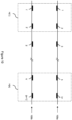
- a Hall element having four terminals can be represented by an equivalent circuit as shown in Fig. 5 .
- the four terminals 1, 2, 3 and 4 are connected via the four resistances R1, R2, R3 and R4 (Wheatstone bridge). If all four resistances are equal, the offset, i.e. the Hall voltage measured in the absence of a magnetic field, is zero. As is well known in the art, if one of the four resistances R1, R2, R3 and R4 is different while the other three resistances are all equal, the offset of the Hall element can be cancelled by application of the current spinning technique. In US 2016/0154066 Al it is shown that the offset can be cancelled provided that the two resistances R1 and R3 or the two resistances R2 and R4 are equal.
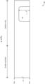
- the four resistances R1, R2, R3 and R4 are indicated for the vertical Hall element 100.
- the geometric dimensions of the vertical Hall element 100 are delineated.
- L denotes the size of the terminals 1 and 2 in direction of the cut A-A'.
- L' denotes the size of the terminals 3 and 4 in direction of the cut A-A'.
- the sizes of the terminals are defined by the lateral dimensions of highly doped regions 103 and 303, respectively.
- T denotes the thickness of the silicon substrate after thinning.
- P denotes the distance between the center of terminal 1 and the center terminal 2 on the first surface 101a.
- the distance between the center of terminal 3 and center of terminal 4 on the second surface is also P.
- D denotes the distance between the edge of the terminal 1 and the boundary of the well 102 along cut direction A-A'.
- the distance between the edge of terminal 2 and the boundary of well 102 on the right side of Fig. 7 is D as well.
- the distance D can also be zero.
- the resistances R2 and R4 are not necessarily equal. Possible causes for a difference between R2 and R4 are, for example, a doping gradient of the well 102, a difference in the contact resistances on the first and the second surface, or the additional series resistance associated with the through silicon vias.
- the size L' of the terminals 3 and 4 can be adjusted with respect to the size L of the terminals 1 and 2 such that the resistances R2 and R4 are approximately same.
- the resistances R1 and R4 are not necessarily equal. However, as a matter of fact, for given substrate thickness T and distance D to the boundary of the well 102, the distance P between terminal 1 and terminal 2 can be adjusted such that resistances R1 and R4 are approximately same.
- the vertical Hall element can be represented by a Wheatstone bridge with the four resistances R1, R2, R3 and R4 having all nearly the same value.
- the vertical Hall element has a nearly four-fold symmetry.
- the Hall voltage acquired between the terminals 4 and 2 is again representative for a magnetic field perpendicular to plane of the terminal 1, 2, 3 and 4.
- the terminal 4 can be connected to a current source and terminal 2 be connected to ground.
- the Hall voltage acquired between the terminals 1 and 3 is again representative for a magnetic field perpendicular to plane of the terminal 1, 2, 3 and 4.
- the offset for each single phase of operation is already low.
- a very small value for the residual offset can be obtained.
- the current spinning technique can be combined with orthogonal coupling of two or four Hall elements to further reduce the residual offset.
- Fig. 40 and 41 show the vertical Hall element 600, which represents another embodiment of the invention.
- the vertical Hall element 600 is depicted from above, looking on the first silicon surface.
- Fig. 41 shows the vertical Hall element 600 along the cut direction A-A' indicated in Fig. 40 .
- the vertical Hall element 600 is formed on the semiconductor substrate 101, which might be a low doped silicon substrate having the first conductivity type.
- the Hall terminals 1 and 2 formed on the first surface 101a are in contact with the well 102, which extends from the first surface 101a into the substrate and which is exposed at the second surface 101b.
- the two Hall terminals 3 and 4 formed on the second surface are in contact with the well 102.
- the vertical Hall element of the second embodiment is characterized in addition by a high degree of linearity.
- the vertical Hall element 700 is formed on a semiconductor substrate 1001 having the first conductivity type, which is either p-type or n-type.
- the terminals 1 and 2 are disposed on the first surface 1001a with the highly doped regions 103 having the first conductivity type, i.e. the same conductivity type as the substrate 1001.
- the terminals 3 and 4 are disposed on the second surface 101b obtained by thinning of the primary substrate from the second side.
- the highly doped regions 303 have the first conductivity type as well.
- T700 denotes the thickness of the substrate 1001.
- Fig. 8 and 9 show a circular vertical Hall element according to another embodiment of the invention.
- the vertical Hall element 200 is depicted from above, looking onto the first surface 101a of the semiconductor substrate 101.
- Fig. 9 provides a circular cut of the vertical Hall element 200 along the indicated path between C and C'.
- the circular vertical Hall element 200 has N terminals disposed on the first surface 101a and N terminals disposed on the second surface 101b of the thinned semiconductor substrate 101.
- the N terminals on the first surface are arranged on a circle and are formed in the ring-shaped well 102.
- the ring-shaped well 102 constitutes the Hall plate or Hall sensor region of the circular vertical Hall element 200.
- the ring-shaped well 102 extends from the first surface 101a and is exposed at the second surface 101b obtained by thinning of the semiconductor substrate 100 from the second side.
- the N terminals on the first silicon surface have equal size and are equally spaced.
- the N terminals disposed on the second surface are also arranged on a circle such that the two circles are concentric and have the same radius.
- the N terminals disposed on the second silicon surface have also equal size, are equally spaced and in are contact with the ring-shaped well 102 being exposed on the second surface.
- the arrangement is such that for each terminal k on the first surface 101a, there is one terminal k' on the second surface 101b, which is located directly below the terminal k, i.e.
- N such vertical Hall sub-elements With N terminals on the first surface and N terminals on the second surface, N such vertical Hall sub-elements can be formed. However, also less than N vertical Hall sub-elements can be formed in this way by increasing the step size. As the N vertical Hall sub-elements in general will not be measured at the same instant of time, they are called temporary vertical Hall elements. During the operation of the k-th vertical Hall sub-element, all terminals that do not belong the k-th vertical Hall sub-element are left open.
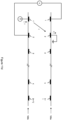
- the third and the fourth phase is presented, respectively.
- a settled Hall voltage of the first temporary vertical Hall element H(1) is obtained.
- the spinning current method is applied to next temporary vertical Hall element H(2).
- spinning current method is applied to the temporary vertical Hall element H(k).
- Fig. 13 and 14 show an alternative embodiment of the invention.
- the circular vertical Hall element 300 is shown from above, looking on the first surface 101a.
- the circular vertical Hall element 300 is shown along the indicated cut in x-direction from D to D'.
- the circular vertical Hall element 300 differs from the circular vertical Hall element 200 only in that there are in addition two ring-shaped isolation structures 301a and 301b.
- the isolation structures 301a and 301b extend from the first surface 101a to the second surface 101b of the thinned silicon substrate.
- the two ring-shaped isolation structures 301a and 301b are concentric with the ring-shaped well 102.
- the area laterally enclosed by the two ring-shaped isolation structures is the well 102.
- a well 102 is formed in the substrate 101 having first conductivity type.
- the well 102 has the second conductivity type.
- the well 102 might be formed by sequence of masked implant steps with varied implant energy.
- the sequence of implant steps may include high energy implants having energies in the MeV range.
- a furnace anneal is applied at a temperature between 1000°C and 1200°C for several hours. Implantation and furnace anneal conditions are optimized towards achieving a uniform dopant concentration in vertical direction.
- Tl denotes the depth of the well 102 after furnace annealing.
- the depth Tl is greater than 4 ⁇ m, and preferable greater than 6 ⁇ m.
- an isolation structure like shallow trench isolation (STI) is not shown. However, it is assumed that shallow trench isolation is applied, and even it might present in the region of the vertical Hall element.
- STI shallow trench isolation
- transistor wells 112 and 113 are formed.
- 112 denotes a p-type well in which an NMOS transistor is formed and 113 denotes an n-type well in which a PMOS transistors is formed.
- the respective depths T2 and T3 of the wells 112 and 113 are lower than the depth Tl of the well 102.
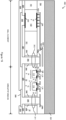
- Fig. 27 shows a semiconductor device 500 having one or more vertical Hall elements 300.
- the semiconductor device 500 could be Hall IC, for instance a Hall IC for angular position measurement.
- semiconductor device 500 comprises one or more vertical Hall elements 300 having the Hall sensor region 102 confined by isolation structures 301.
- Fig. 28 to 39 show the manufacturing steps for the fabrication of the semiconductor device 500.
- the basic manufacturing steps are explained in the patent EP29l3847(Al ), which is incorporated here as a whole.
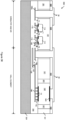
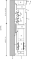
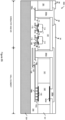
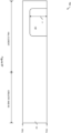
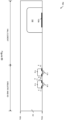
- the Fig. 43 , 44 and 45 show a second embodiment of a vertical Hall element 100.
- the vertical Hall element is shown from above, looking on the first silicon surface. Two cuts are indicated, one cut parallel to the x-direction from A to A', and one cut parallel to the y-direction from B to B'.
- Fig. 44 shows a cross-section of the vertical Hall element 100 along the cut A-A' and
- Fig. 45 shows a cross-section of the vertical Hall element 100 along the cut B-B'.
- the vertical Hall element 100 is formed on a semiconductor substrate 101.
- the semiconductor substrate 101 might be a low doped silicon substrate having the first conductivity type.
- the first conductivity type is preferably p-type.
- the substrate has a first surface 101a and a second surface 101b.
- the two surfaces are opposing and parallel to each other.
- the second surface 101b is obtained by thinning of the substrate from the backside, i.e. from the side opposite to the first surface 101a.
- a doping region 102 is formed, which extends from the first surface 101a to the second surface 10lb.
- the doping region 102 has the second conductivity type, i.e. region 102 has n-type conductivity.
- the region 102 might be doped with Phosphorus and the dopant concentration might be in the range of 1*10 14 /cm 3 to 1*10 17 /cm 3 .
- the dopant concentration is homogeneous in vertical direction.
- the doping regions 152a and 152c are disposed in well 102.
- the doping regions 152a and 152c have the second conductivity type. They might be doped by phosphorus and the dopant concentration might be in the range of 1* 10 17 /cm 3 to 1 * 10 21 /cm 3 .
- the doping regions 152a and 152c are buried in region 102.
- the location of the doping regions 152a and 152c in z-direction is approximately half-way between the first surface 101a and the second surface 101b.
- the wells 103a and 103c having the second conductivity as well.
- the well 103a extends from the first surface 101a into the doping region 102 reaching out to the buried region 152a.
- the well 103c extends from the first surface 101a into the doping region 102 such that the well 103c is in contact with the buried region 152c.
- the highly doped regions 103a, 103b and 103c are formed extending from the first surface into doping region 102.
- the highly doped regions 103a, 103b and 103c have the second conductivity type.
- the dopant concentration might be in the range of 1*10 19 /cm 3 to 1*10 22 /cm 3 .
- the highly doped regions 103a, 103b and 103c are arranged along the x-direction in a row.
- the doping region 103b is located between doping regions 103a and 103c in such a way that the distance between 103a and 103b and the distance between 103b and 103c are equal.
- the highly doped regions 103a, 103b and 103c are disposed inside of region 102.
- the highly doped region 103a is arranged inside of the well 151a and the highly doped region 103c is arranged inside of the well 151c.
- a dielectric layer 104 is disposed on the first surface 101a.
- the dielectric layer 104 may comprise several layers of silicon nitride, silicon oxide or low-k dielectrics as typically used in CMOS manufacturing processes.
- Metal contacts 105a, 105b and 105c are embedded in the dielectric layer 104.
- the metal contact 105a is placed on the highly doped region 103a achieving an electrical connection to the highly doped region 103a and thus to the well 151a and further to the buried region 152a.
- the metal contact 105b is placed on the highly doped region 103b achieving an electrical connection to the highly doped region 103b.
- the metal contact 105c is placed on the highly doped region 103c achieving an electrical connection to the highly doped region 103c and thus to the well 151c and further to the buried region 152c.
- a plurality of metal contacts might be placed on the highly doped region 103b, and similarly, also on the highly doped regions 103a and 103c.
- a metal silicide might be formed on the highly doped regions 103a, 103b and 103c.
- the metal contacts 105a, 105b and 105c might consist of tungsten or other suitable metal.
- a first metal layer is shown being embedded in the dielectric layer 104.
- a CMOS metallization may comprise several metal layers and vertical interconnects. For simplicity, only one metal layer is shown in Fig. 44 and 45 .
- 106a, 106b and 106c denote metal wires formed by this first metal layer, connecting to metal contacts 105a, 105b and 105c, respectively.
- the metal wire 106b is oriented along the y-direction. Also, the metal wires 106a and 106c are oriented along the y-direction.
- a carrier 201 is attached to the top surface 104a of the dielectric layer 104. The carrier 201 might be a silicon wafer.
- a fourth shallow highly doped region is formed, which is denoted by 303d.
- the highly doped region 303d extends from the second surface 101b into the doping region 102.
- the doping region 303d has the second conductivity type and a dopant concentration in the range of 1*10 19 /cm 3 to 1*10 22 /cm 3 .
- the doping region 303d has the same but opposite location of the doping region 103b. More precisely, if a connecting line is drawn from the center of the doping region 103b at the first surface 101a to the center of the doping region 303d at the second surface 101b, then this connecting line is perpendicular to the surfaces 101a and 101b.
- a dielectric layer 304 is disposed on the second surface 101b. The dielectric layer may consist of silicon oxide.
- a metal contact 305d is formed in the dielectric layer 304 such that an electrical connection is established to the highly doped region 303d.
- the metal contact 305d may extend to a metal wiring formed on the dielectric layer 304 as shown in Fig. 43 and 44 .
- the metal wiring is oriented parallel to the y-direction as indicated in Fig 44 .
- Metal contact and wiring 305b might consist of aluminium.
- the contact hole formed in the dielectric layer 304 might be filled with tungsten.
- the wiring part of 305d disposed on the dielectric layer 304 might consist of aluminium or copper. Other metallization schemes could be conceived as well.
- a passivation layer 308 is disposed on metal wire 305d and dielectric layer 308.
- the passivation layer 308 might consist of silicon oxide, silicon nitride, silicon oxynitride or a layered stack of these materials.
- the doping wells 153 which extend from the first surface 101a into the doping region 102.
- the two doping wells 153 are placed each between the highly doped region 103b in the center and the two highly doped regions 103a and 103c on left and on the right side, respectively.
- the two doping wells 153 might each be butted to the wells 151a and 151c, respectively.
- the wells 153 might have a similar depth as the well 151a and 151c and might, as shown in Fig. 43 , reach down to the buried doping regions 152a and 152c.
- the doping wells 153 have the first conductivity type.
- Fig. 45 showing again the vertical Hall element 100 in cut direction B-B'.
- the doping region 102 constitutes the Hall sensor region or Hall plate of the vertical Hall element 100.
- the doping region 102 is laterally, i.e. in x- and in y-direction bounded by a p-n junction formed with the substrate 101 having the reverse polarity of well 102.
- Fig. 46 showing again the vertical Hall element 100 in cut direction A- A'.
- the vertical Hall element 100 has four Hall terminals, which are indicated by the capital letters A, B, C and D.
- the Hall terminal B is arranged on the first surface 101a.
- the terminal B of the vertical Hall element 100 is defined by the spatial dimensions of the highly conductive region 103b.
- the Hall terminal D is arranged on the first surface 101b opposite to terminal B. Again, from an operation point view the terminal D of the vertical Hall element 100 is defined by the spatial dimensions of the highly conductive region 303d.
- the Hall terminal A comprises the highly conductive buried region 152a with the well 151a providing a connection to the first surface, where terminal A is accessed via highly doped region 103a and metal contacts placed thereon.
- the terminal C comprises the highly conductive buried region 152a with the well 151c providing a connection to the first surface 101a, where the terminal C is accessed via highly doped region 103c and metal contacts placed thereon.
- the wells 153 which have the reverse polarity of the doping regions 102, 151a, 152a, 151c and 152c, serve to shield the active sensor region between the four Hall terminals electrostatically from the wells 151a and 151c.
- Fig. 46 four arrows are drawn, indicated by the numbers 1, 2, 3 and 4. Each arrow represents the direction of the operating current driven through the Hall sensor region.
- the four arrows are thus representative of the four possible operations modes or phases of the vertical Hall element.
- operation mode 1 a current is forced between terminals B and D flowing in the direction from terminal B to terminal D.
- a Hall voltage is acquired between terminal C and terminal D, which is indicative of a magnetic field component pointing in y-direction.
- operation mode 2 a current is forced between terminal C and A flowing in direction from terminal C to terminal A.
- a Hall voltage is acquired between terminals Band C, which is again indicative of a magnetic field component pointing in y-direction.
- the operation mode 3 corresponds to operation mode 1 with the difference that the current direction is reversed, and the Hall voltage is required between terminal D and C.
- the operation mode 4 corresponds to operation mode 2 with the current direction reversed and the terminals B and D commutated with respect to operation mode 2.
- a current can be forced through the Hall element 100, which is essentially flowing vertically through the Hall sensor region 102.
- a current can be forced through the Hall sensor element, which is essentially flowing parallel to the first surface 101a at a certain depth being determined by the depth of the highly conductive regions 152a and 152c.
- the specific Hall terminal configuration of vertical Hall element 100 with two buried terminals (A and C), one terminal on first surface 101a (B) and one terminal on second surface 101b (D) allows in principle to achieve a higher voltage-related sensitivity than can be obtained typically in a conventional vertical Hall element with all terminals arranged on the primary surface of the substrate.
- the vertical Hall element 100 can be designed such that the offset, i.e. the Hall voltage measured at zero magnetic field, is low for each of the four operation modes.
- Important design parameters are the thickness of the substrate 101 (the distance between the first surface 101a and the second surface 101b), the depth of the highly conductive regions 152a and 152b, the lateral spacing the depth of the highly conductive regions 152a and 152b, and the spatial dimensions of the highly doped regions 103b and 303d.
- the highly doped regions 103a, 103b and 103c are arranged along the x-direction in a row with highly doped region 103b placed in the middle between highly doped regions 103a and 103c.
- the highly doped region 303d has the same but opposite location as the highly doped region 103b.
- the methods of optimization such as TCAD simulation and design of experiment are known in the art.
- TCAD simulation and design of experiment are known in the art.
- the offset can further be reduced by averaging over the four operation modes.
- Current spinning and orthogonal coupling of two or four Hall elements are known techniques, which are regularly adopted in the industry and which could be applied to the vertical Hall element 100 as well.
- the vertical Hall element 200 is shown, which represents another embodiment of the inventive concept.
- the Hall element 200 differs from the Hall element only in that the shielding wells 153 are missing.
- FIG. 48 Another embodiment of the invention is presented in Fig. 48 showing the vertical Hall element 300 in a cut along the x-direction.
- the connecting wells 151a and 151c are surrounded each by a dielectric structure denoted by 154.
- the dielectric structure 154 might have a similar depth as the well 151a and 151c.
- the well 151a might laterally (i.e. in the x-y-plane) be enclosed by the dielectric structure 154 and, in the same fashion, the well 151c might laterally be enclosed by a second dielectric structure 154.
- the dielectric structure may consist of silicon oxide or another dielectric material.
- the dielectric structure 154 might also be a trench having a liner consisting of dielectric material such as silicon oxide and further being filled with poly-silicon.
- the dielectric structure 154 enhances the shielding of the wells 151a and 151c strengthening the buried character of terminals A and C.
- the vertical Hall element 400 differs from the vertical Hall element 300 by the fact that the buried regions 152a and 152c are missing.
- buried terminals A and C are defined by the wells 151a and 151c, respectively.
- the wells 151a and 151c are enclosed each by the dielectric structures 154.
- the wells 151a and 151c are in electrical contact with the Hall sensor region 102 only at their bottom surfaces.
- the depth of the wells 151a and 151c, and accordingly also the depths of the dielectric structures 154 is increased.
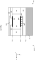
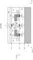
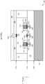
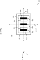
- the vertical Hall element 500 differs from the vertical Hall element 100 in that doping region 102 establishing the Hall sensor region is separated by a deep trench isolation structure 301 from the substrate 101. In z-direction the deep trench isolation structure 301 extends from the first surface 101a to the second surface 101b of the substrate 101 as shown in Fig. 51 and 52 .
- the doping region 102 is in x- and y-direction enclosed by the deep trench isolation structure.
- the enclosure is such that the doping region 102 extends in x- and y-direction everywhere to the deep trench isolation structure 301.
- the well 102 has no boundary with substrate 101.
- depletions zones are formed along all p-n junctions delimiting the Hall sensor region.
- the Hall sensor region 102 of vertical Hall element 500 has no p-n junction boundary with the surrounding substrate 101 anymore, no depletion zones can be formed at this boundary anymore.
- depletion zones are formed during operation of the vertical Hall element 500 along the shielding wells 153, which have the first conductivity.
- the shielding wells 153 in the vertical Hall element 500 are removed and substituted by a dielectric isolation structure 154 like in the vertical Hall element 300.
- the Hall sensor region 102 is not bounded at any instance by a p-n junction anymore.
- Depletions zones formed at the boundaries of the Hall plate during operation of the Hall element change the resistance of the Hall plate affecting sensitivity and offset. Since the width of the depletion zones is a function of the operating current, the Hall element will display a non-linear behaviour. This non-linearity increases the calibration effort and the associated cost.
- Figure 53 is another representation the vertical Hall element 100 along the cut direction B-B'.
- a through silicon via (TSV) is depicted on the right side of Figure 53 .
- the through silicon via provides a vertical conductive path through the substrate 101 connecting the highly doped region 303d disposed on the second surface 101b and representing terminal D to the metal wiring formed on the first silicon surface.
- the through silicon via associated with the terminal D is denoted by TSV(D).
- the through silicon via TSV(D) is in contact with the portion 106d of the first metal layer embedded in the dielectric layer 104.
- the through silicon via TSV(D) is connected to the terminal D by the metal wiring 305d.
- the terminal D can be accessed at the point C(D).
- the terminal B formed on the first surface 101a can be accessed electrically at point C(B).
- the through silicon via is filled with a conductive material 305d which could be the same material which is used for the metallization on the second surface.
- the conductive filling 305d of the through silicon via is isolated from the silicon substrate 101 by the dielectric liner 306 disposed onto the inner surfaces of the through silicon via.
- the through silicon via is placed at a distance L from the well 102 in which the Hall terminals are formed. A current I driven through the through silicon via gives rise to a magnetic field parallel to the silicon surface.
- the distance L can be set large enough. For instance, if the Hall current is 1mA and the distance L is set to 100 ⁇ m, the induced magnetic field strength is 2 ⁇ T, which is well below the measurement resolution of available vertical Hall elements.
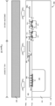
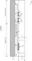
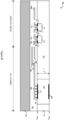
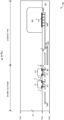
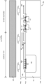
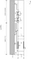
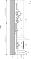
- Figure 54 show a third embodiment of a semiconductor device 600 comprising a vertical Hall element.
- Figures 55 to 65 illustrate manufacturing steps of a method of manufacturing the third embodiment of a semiconductor device 600 comprising a vertical Hall element.
- the basic manufacturing steps are explained in the patent EP2913847(A1 ), which is incorporated here as a whole.
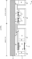
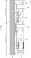
- Figure 66 show a fourth embodiment of a semiconductor device 700 comprising a vertical Hall element.
- Figures 67 to 78 illustrate manufacturing steps of a method of manufacturing the fourth embodiment of a semiconductor device 700 comprising a vertical Hall element.
Landscapes
- Engineering & Computer Science (AREA)
- Manufacturing & Machinery (AREA)
- Hall/Mr Elements (AREA)
- Metal-Oxide And Bipolar Metal-Oxide Semiconductor Integrated Circuits (AREA)
- Measuring Magnetic Variables (AREA)
- Internal Circuitry In Semiconductor Integrated Circuit Devices (AREA)
- Semiconductor Integrated Circuits (AREA)
Abstract
Description
- The disclosure relates to a vertical Hall element having reduced offset and a method of manufacturing thereof.
- Magnetic sensor ICs typically use silicon-based Hall elements which are monolithically integrated with the electrical circuits required for signal conditioning and amplification. Typical commercial products with monolithically integrated Hall elements are Hall switch ICs, Hall ICs for linear position measurement, angular position sensor Hall ICs, Hall ICs for current sensing and 3D Hall sensor ICs. Depending on the product type, a Hall IC may include horizontal Hall elements, vertical Hall elements, or both. Vertical Hall elements, which sense the strength of the magnetic field in a direction lying in the plane of the silicon surface, are used in angular position sensor Hall ICs and, together with a horizontal Hall element, in 3D Hall sensor ICs.
- Conventional vertical Hall elements are formed as follows: a well having n-type conductivity is formed in the low-doped p-type silicon substrate. The n-type well constitutes the Hall plate of the sensor being isolated from the substrate by a p-n junction. Three, four, five or more Hall terminals are formed on the silicon surface within the region of the n-type well, typically arranged in a row or on a circle (R. S. Popovic, "Hall Effect Devices", Institute of Physics Publishing, Bristol and Philadelphia 2004).
- In these conventional vertical Hall elements, the sensitivity is limited by the finite depth of the n-type well in which the Hall terminals are placed. For this reason, oftentimes high-voltage CMOS processes having deep wells are used for manufacturing Hall ICs with vertical Hall elements. Even in these processes, well depths are generally only in the order of a several micrometers.
- Besides low sensitivity, conventional vertical Hall elements typically suffer from high residual offsets. The offset of a Hall element, i.e. the Hall voltage measured at zero magnetic field strength, can be reduced by known techniques such as current spinning, orthogonal coupling or a combination thereof. Effective offset reduction relies on commutation of Hall terminals as well as on the four-fold symmetry of the Hall device. Single conventional vertical Hall elements having their terminals placed all on the same silicon surface deviate necessarily from an ideal four-fold symmetry.
- Another disadvantage of a conventional vertical Hall element is its non-linearity. As the n-type Hall plate is formed in the p-type substrate, a depletion zone is formed along the p-n junction during the operation of the Hall element, i.e. when a current is forced through the Hall element. The width of the depletion zone varies spatially and depends on the exact operation condition. In any case, the formation of a depletion region alters the effective resistance of the Hall plate giving rise to a non-linear behavior of the vertical Hall element. The non-linearity makes also the offset cancellation of the Hall element more difficult.
-
US 2012/169329 A1 discloses a Hall sensor element having a substrate, which has a main surface, having an electrically conductive active region, which extends from the main surface into the substrate, and having a first electrically conductive, buried layer in the substrate, which contacts the active region at a first lower contact surface. A method for measuring a magnetic field with the aid of such a Hall sensor element is also disclosed, in which an electrical measuring current is conducted through the active region between a first upper contact electrode at the main surface and the first lower contact surface. A Hall voltage is picked up in the active region along a path running inclined with respect to a connecting line between the first lower contact surface and the first upper contact electrode. Alternatively, a measuring current is conducted through the active region over such a path, and a Hall voltage is picked up between the first upper contact electrode and the first lower contact surface. -
US 2006/170406 A1 discloses a Hall element, wherein a N-type epitaxial layer is formed on a p-type silicon substrate. Four N+ regions (diffusion regions used as electrodes) are formed in the N-type epitaxial layer. An insulation layer having a fixed depth is formed around each of the N+ regions on a principal surface of an epitaxial layer. The insulation layer restricts a current path region formed between the N+ regions. Side surfaces of the N+ regions are covered by the insulation layer. The N+ regions are brought into contact with the epitaxial layer by a bottom surface exposed from the insulation layer. - There is a desire to provide a vertical Hall element with improved characteristic parameters, such as an effective offset reduction, a high sensitivity and high degree of linearity.
- An embodiment of the vertical Hall element that provides improved characteristic parameters is specified in
claim 1. Further embodiments are specified inclaims 2 to 6. - The following possible embodiments, which are described in this part of the disclosure, are not included in the scope of the claims, and are only for information purpose.
- According to a possible embodiment of a vertical Hall element, the vertical Hall element comprises a substrate of a first conductivity type having a first surface and a second surface. The vertical Hall element further comprises a well being disposed in the substrate, the well having a second conductivity type. The well is exposed on the second surface of the substrate. The vertical Hall element comprises at least two terminals arranged on the first surface of the substrate and being in contact with the well. The vertical Hall element further comprises at least two terminals arranged on the second surface of the substrate and being in contact with the well.
- The at least two terminals on the second surface of the substrate are disposed in an orthogonal projection on the substrate below the at least two terminals on the first surface of the substrate.
- According to a possible embodiment of the vertical Hall element, the at least two terminals on the first surface of the substrate comprises a first terminal and a second terminal being arranged next to each other on the first surface of the substrate. The at least two terminals on the second surface of the substrate comprises a third terminal and a fourth terminal being arranged next to each other on the second surface of the substrate. The fourth terminal is located directly below the first terminal such that a virtual straight line between a center of the first terminal and a center of the fourth terminal is perpendicular to first and second surface of the substrate. The third terminal is located directly below the second terminal such that a virtual straight line between a center of the second terminal and a center of the third terminal is perpendicular to first and second surface of the substrate.
- According to a possible embodiment of the vertical Hall element, each of the at least two terminals on the first surface of the substrate comprises a shallow and highly doped region extending from the first surface into the substrate, the highly doped region having the second conductivity type. According to a possible embodiment of the vertical Hall element, the vertical Hall element comprises a dielectric layer being disposed on the first surface of the substrate, and a wiring being embedded in the dielectric layer. The at least two terminals on the first surface of the substrate may be connected with a first metal layer of the wiring embedded in the dielectric layer.
- According to a possible embodiment of the vertical Hall element, the vertical Hall element comprises a carrier substrate being bonded to a top surface of the dielectric layer. The top surface of the dielectric layer is opposite to a surface of the dielectric layer disposed on the first surface of the substrate.
- According to a possible embodiment of the vertical Hall element, each of the at least two terminals on the second surface of the substrate comprises a shallow and highly doped region extending from the second surface into the substrate, the highly doped region having the second conductivity type.
- According to a possible embodiment of the vertical Hall element, the vertical Hall element comprises a second dielectric layer and a passivation layer. The second dielectric layer is disposed on the second surface of the substrate and the passivation layer is disposed on the dielectric layer.
- According to a possible embodiment of the vertical Hall element, the vertical Hall element comprises a through silicon via filled with a conductive filling that provides a vertical conductive path through the substrate for connecting one of the third and fourth terminal to the wiring in the dielectric layer. The conductive filling of the through silicon via is isolated from the substrate by a dielectric liner disposed onto an inner surface of the through silicon via.
- According to a possible embodiment of the vertical Hall element, the vertical Hall element comprises a deep trench isolation structure extending from the first surface of the substrate to the second surface of the substrate so that the well is isolated from the substrate by the deep trench isolation structure.
- According to another possible embodiment of the vertical Hall element, the vertical Hall element is configured as a circular vertical Hall element. The well is formed as a ring-shaped well. The vertical Hall element has a plurality of the at least two terminals located on the first surface of the substrate on a first circle and being in contact with the well, and a plurality of the at least two terminals located on the second surface of the substrate on a second circle and in contact with the well. A respective one of the plurality of the at least two terminals on the second surface of the substrate is disposed in an orthogonal projection on the substrate below a respective one of the plurality of the at least two terminals on the first surface of the substrate.
- According to a possible embodiment of the vertical Hall element, the vertical Hall element comprises two ring-shaped isolation structures. The two ring-shaped isolation structures extend from the first surface of the substrate to the second surface of the substrate and are concentric with the ring-shaped well so that the well is laterally enclosed by the two ring-shaped isolation structures and isolated from the substrate.
- According to a possible embodiment, the vertical Hall element has two terminals on the first surface and two terminals on the second surface of a thinned semiconductor substrate of first conductivity type. The four terminals are arranged such that one terminal on the first surface and one terminal on the second surface each have the same but opposite location. The two terminals on the first surface are formed in a well having the second conductivity type. The well is exposed on the second surface such that also the terminals on the second surface are in contact with the well. The geometry of the vertical Hall element is defined such that the four resistances between the four terminals are nearly equal. The terminals on the second surface are connected by through silicon vias to the wiring on the first surface.
- According to another possible embodiment, the vertical Hall element has two terminals on the first surface and two terminals on the second surface of a thinned semiconductor substrate of first conductivity type. The four terminals are arranged such that one terminal on the first surface and one terminal on the second surface each have the same but opposite location. The two terminals on the first surface are formed in a well having the second conductivity type. The well is exposed on the second surface such that also the terminals on the second surface are in contact with the well. The well is enclosed by a deep trench isolation extending from the first surface to the second surface of the thinned semiconductor substrate. The geometry of the vertical Hall element is defined such that the four resistances between the four terminals are nearly equal. The terminals on the second surface are connected by through silicon vias to the wiring on the first surface.
- According to another possible embodiment, the vertical Hall element has two terminals on the first surface and two terminals on the second surface of a thinned semiconductor substrate of first conductivity type. The four terminals are arranged such that one terminal on the first surface and one terminal on the second surface each have the same but opposite location. The four terminals are enclosed by a deep trench isolation, which extends from the first surface to the second surface of the thinned semiconductor substrate. The geometry of the vertical Hall sensor is defined such that the four resistances between the four terminals are nearly equal. The terminals on the second surface are connected by through silicon vias to the wiring on the first surface.
- According to another possible embodiment, the vertical Hall element has N terminals on the first surface and N terminals on the second surface of a thinned semiconductor substrate of first conductivity type. The N terminals on the first surface have the same size, are equally spaced and are arranged on a circle. The N terminals on the second surface, having also same size, are placed such that for each terminal on the first surface there is one terminal on the second surface having the same but opposite location. The N terminals on the first surface are formed in a ring-shaped well having the second conductivity type. The well is exposed on the second surface such that also the N terminals on the second surface are in contact with the ring-shaped well. The geometry of the vertical Hall element is defined such that the four resistances between the four terminals of each temporary vertical Hall element, that can be formed along the circle, are nearly equal. The N terminals on the second surface are connected by N through silicon vias to the wiring on the first surface.
- According to another possible embodiment, the vertical Hall element has N terminals on the first surface and N terminals on the second surface of a thinned semiconductor substrate of first conductivity type. The N terminals on the first surface have same size, are equally spaced and are arranged on a circle. The N terminals on the second surface, having also the same size, are placed such that for each terminal on the first surface there is one terminal on the second surface having the same but opposite location. The N terminals on the first surface are formed in a ring-shaped well having the second conductivity type. The well is exposed on the second surface such that also the N terminals on the second surface are in contact with the ring-shaped well. The ring-shaped well is laterally separated from semiconductor substrate by two deep trench isolation rings. The two deep trench isolation rings extend from first surface to the second surface of the thinned semiconductor substrate. The geometry of the vertical Hall element is defined such that the four resistances between the four terminals of each temporary vertical Hall element, that can be formed along the circle, are nearly equal. The N terminals on the second surface are connected by N through silicon vias to the wiring on the first surface.
- A second embodiment of a vertical Hall sensor element that provides improved characteristic parameters is specified in
claims 1 to 6. - According to this second possible embodiment of a vertical Hall element, the Hall element comprises a substrate of a first conductivity type having a first surface and a second surface, and a well being disposed in the substrate. The well has a second conductivity type. The vertical Hall element comprises a first terminal, a second terminal, a third terminal and a fourth terminal. Each of the first and third terminal comprises a connecting region. The respective connecting region provides a connection of the first and second terminal to the first surface of the substrate. Each of the first and third terminal is accessed via a doped region extending from the first surface of the substrate inside of the doped region. The second terminal is arranged on the first surface of the substrate. The fourth terminal is arranged on the second surface of the substrate opposite to the second terminal.
- According to this second possible embodiment of the vertical Hall element, the second terminal comprises a conductive region extending from the first surface of the substrate in the substrate. The fourth terminal comprises a conductive region extending from the second surface of the substrate in the substrate. The fourth terminal is located directly below the second terminal such that a virtual straight line between a center of the conductive region of the second terminal and a center of the conductive region of the fourth terminal is perpendicular to first and second surface of the substrate.
- According to this second possible embodiment of the vertical Hall element, the vertical Hall element comprises a dielectric layer being disposed on the first surface of the substrate. The vertical Hall element further comprises a carrier being attached to a top surface of the dielectric layer, wherein the top surface of the dielectric layer is opposite to a surface of the dielectric layer disposed on the first surface of the substrate.
- According to this second possible embodiment of the vertical Hall element, each of the first and third terminal comprises a conductive buried region buried in the well. The respective connecting region provides a connection of the conductive buried region to the first surface of the substrate.
- According to this second possible embodiment of the vertical Hall element, the vertical Hall element comprises a first doping well extending form the first surface of the substrate into the well down to the buried region of the first terminal. The vertical Hall element comprises a second doping well extending form the first surface of the substrate into the well down to the buried region of the third terminal.
- According to this second possible embodiment of the vertical Hall element, the connecting well of the first terminal is surrounded by a first dielectric structure. The connecting well of the third terminal is surrounded by a second dielectric structure.
- According to this second possible embodiment of the Hall vertical element, the vertical Hall element comprises a deep trench isolation structure extending from the first surface to the second surface of the substrate. The well is isolated by the deep trench isolation structure from the substrate.
- A semiconductor device comprising a vertical Hall element of any of the claims is specified in claim 7. The semiconductor device further comprises a circuitry to operate the vertical Hall element, wherein the circuitry is configured as an integrated circuit being formed in the substrate.
- According to a possible embodiment of the semiconductor device, the circuitry comprises a bonding pad formed on the second surface of the substrate. The circuitry comprises a through silicon via to provide a connection between the bonding pad and a wiring disposed in dielectric layer on the first surface of the substrate.
- Additional features and advantages are set forth in the detailed description that follows and in part will be readily apparent to those skilled in the art from the description or recognized by practising the embodiments as described in the written description and claims hereof, as well as the appended drawings. It is to be understood that both the foregoing general description and the following detailed description are merely exemplary, and are intended to provide an overview or framework to understand the nature and character of the claims.
- The accompanying drawings are included to provide further understanding, and are incorporated in and constitute a part of the specification. The drawings illustrate one or more embodiments, and together with the detailed description serve to explain principles and operation of the various embodiments. As such, the disclosure will become more fully understood from the following detailed description, taken in conjunction with the accompanying figures.
-
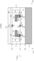
Figures 1 to 7 show a first embodiment of a vertical Hall element, which is not included in the scope of the claims; -
Figures 8 to 14 show modifications of the first embodiment of a vertical Hall element, which are not included in the scope of the claims; -
Figure 15 shows a first embodiment of a semiconductor device comprising a vertical Hall element, which is not included in the scope of the claims; -
Figures 16 to 26 illustrate manufacturing steps of a method of manufacturing the first embodiment of a semiconductor device comprising a vertical Hall element, which are not included in the scope of the claims; -
Figure 27 show a second embodiment of a semiconductor device comprising a vertical Hall sensor; -
Figures 28 to 39 illustrate manufacturing steps of a method of manufacturing the second embodiment of a semiconductor device comprising a vertical Hall element; -
Figures 40 to 42 show another modification of the first embodiment of a vertical Hall element, which is not included in the scope of the claims; -
Figures 43 to 49 show a second embodiment of a vertical Hall element, according to the present invention. -
Figures 49 to 53 show modifications of the second embodiment of a vertical Hall element, according to the present invention. -
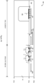
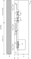
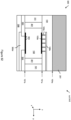
Figure 54 show a third embodiment of a semiconductor device comprising a vertical Hall element, which is not included in the scope of the claims; -
Figures 55 to 65 illustrate manufacturing steps of a method of manufacturing the third embodiment of a semiconductor device comprising a vertical Hall element, which is not included in the scope of the claims; -
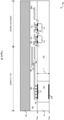
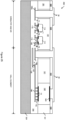
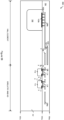
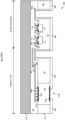
Figure 66 show a fourth embodiment of a semiconductor device comprising a vertical Hall element, which is not included in the scope of the claims; and -
Figures 67 to 78 illustrate manufacturing steps of a method of manufacturing the fourth embodiment of a semiconductor device comprising a vertical Hall element, which is are included in the scope of the claims. - In the following section of the disclosure several embodiments are described which are not included in the scope of the claims, but which are for information only.
- Reference is now made in detail to various embodiments, examples of which are partly illustrated in the accompanying drawings. Whenever possible, the same or like reference numbers and symbols are used throughout the drawings to refer to the same or like parts. The drawings are not necessary to scale, and one skilled in the art will recognize where the drawings have been simplified to illustrate the key aspects of the disclosure. The claims as set forth below are incorporated into and constitute part of this detailed description.
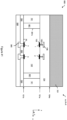
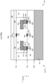
- The
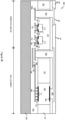
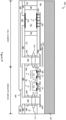
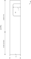
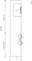
Fig. 1 ,2 and3 show thevertical Hall element 100. InFig. 1 the vertical Hall element is shown from above, looking on the first silicon surface. Two cuts are indicated, one cut parallel to the x-direction from A to A', and one cut parallel to the y-direction from B to B'.Fig. 2 shows a cross-section of thevertical Hall element 100 along the cut A- A' andFig. 3 shows a cross-section of thevertical Hall element 100 along the cut B-B'. Thevertical Hall element 100 is formed on asemiconductor substrate 101. Thesemiconductor substrate 101 might be a low doped silicon substrate having the first conductivity type. The first conductivity type is preferably p-type. The substrate has afirst surface 101a and asecond surface 101b. The two surfaces are opposing and parallel to each other. Thesecond surface 101b is obtained by thinning of the substrate from the backside, i.e. from the side opposite to thefirst surface 101a. Thevertical Hall element 100 is formed in a well 102 having the second conductivity type. The well 102 extends from thefirst surface 101a and is exposed at thesecond surface 101b. The well 102 forms the Hall plate or defines the Hall sensor region of thevertical Hall element 100. Thevertical Hall element 100 has four terminals which are indicated by thenumbers terminals first silicon surface 101a, and theterminals second silicon surface 101b. Theterminals first surface 101a are in contact with thewell 102. Likewise, theterminals second surface 101b are in contact with thewell 102. The twoterminals terminals terminal 4 is located directly belowterminal 1 in the sense that a virtual straight line between the center ofterminal 1 and the center ofterminal 4 is perpendicular to thesilicon surface 101a. Theterminal 3 is located directly below theterminal 2 in the same sense. For each of the two terminals arranged on thefirst surface 101a, a shallow and highly dopedregion 103 is formed extending from the first surface into the substrate. The highlydoped regions 103 have the second conductivity type, which is the conductivity type of thewell 102. The highlydoped regions 103 might be silicided with some metal like cobalt.Metal contacts 105 are formed in thedielectric layer 104 connecting the highlydoped regions 103 with metal lines of afirst metal layer 106 embedded in thedielectric layer 104. Thesubstrate 101 is bonded onto acarrier substrate 201 with thetop surface 104a of thedielectric layer 104. Thecarrier substrate 201 can be silicon substrate as well. At thesecond surface 101b shallow and highlydoped regions 303 are formed for each of the twoterminals second surface 101b into the substrate. The highlydoped regions 303 have the second conductivity type, which is the conductivity type of thewell 102. Adielectric layer 304 is disposed on thesecond surface 101b. Thedielectric layer 304 is structured in such a way that contact holes are formed connecting the highlydoped regions 303. Ametal 305 is deposited into the hole contacts. Furthermore, themetal 305 is structured such that metal wires are formed on the second surface of the substrate. Apassivation layer 308 is disposed on thedielectric layer 304 and themetal layer 305. -
Fig. 4 is another representation thevertical Hall element 100 along the cut direction B-B'. To complementFig. 3 , a through silicon via (TSV) is depicted on the right side ofFigure 4 . The through silicon via provides a vertical conductive path through thesubstrate 101 connecting theterminal 3 disposed on thesecond surface 101b to the metal wiring formed on the first silicon surface. The through silicon via associated with theterminal 3 is denoted by TSV(3). For each terminal disposed on thesecond surface 101b there is one through silicon via connecting the terminal to the wiring formed on the first surface. As thevertical Hall element 100 has two terminals placed on the second surface, there are also two through silicon vias. The through silicon via TSV(3) is in contact with theportion 106 of the first metal layer embedded in thedielectric layer 104. At thesecond surface 101b, the through silicon via TSV(3) is connected to theterminal 3 by themetal wiring 305. In this way, theterminal 3 can be accessed at the point C(3). As shown inFig. 4 , theterminal 2 formed on thefirst surface 101a can be accessed electrically at point C(2). The through silicon via is filled with aconductive material 305 which could be the same material which is used for the metallization on the second surface. For example, this material could be Aluminium. However, other metallization schemes could be considered as well. In one scheme the metal disposed in the through silicon is copper or tungsten, while the metal used for the wiring and for the filling of the contact holes connecting the highlydoped regions 303 is aluminium. In another scheme, the metal disposed in the through silicon via and the metal disposed in the contact holes connecting the highlydoped regions 303 is tungsten, while the metal used for wiring on the second surface is aluminium. The conductive filling 305 of the through silicon via is isolated from thesilicon substrate 101 by thedielectric liner 306 disposed onto the inner surfaces of the through silicon via. The through silicon via is placed at a distance L from the well 102 in which the Hall terminals are formed. A current I driven through the through silicon via gives rise to a magnetic field parallel to the silicon surface. The strength of the induced magnetic field at the location of the vertical Hall element is B = µ0/(2πL)·I. To minimize this perturbing effect, the distance L can be set large enough. For instance, if the Hall current is 1mA and the distance L is set to 100µm, the induced magnetic field strength is 2µT, which is well below the measurement resolution of available vertical Hall elements. - A Hall element having four terminals can be represented by an equivalent circuit as shown in
Fig. 5 . The fourterminals US 2016/0154066 Al it is shown that the offset can be cancelled provided that the two resistances R1 and R3 or the two resistances R2 and R4 are equal. - In
Fig. 6 the four resistances R1, R2, R3 and R4 are indicated for thevertical Hall element 100. InFig. 7 the geometric dimensions of thevertical Hall element 100 are delineated. L denotes the size of theterminals terminals doped regions terminal 1 and thecenter terminal 2 on thefirst surface 101a. Since theterminal 4 has the same but opposite location ofterminal 1 andterminal 3 has the same but opposite location ofterminal 2, the distance between the center ofterminal 3 and center ofterminal 4 on the second surface is also P. D denotes the distance between the edge of theterminal 1 and the boundary of the well 102 along cut direction A-A'. The distance between the edge ofterminal 2 and the boundary of well 102 on the right side ofFig. 7 is D as well. The distance D can also be zero. - For the
vertical Hall element 100 as shownFig. 6 and7 , the resistances R2 and R4 are not necessarily equal. Possible causes for a difference between R2 and R4 are, for example, a doping gradient of the well 102, a difference in the contact resistances on the first and the second surface, or the additional series resistance associated with the through silicon vias. However, as a matter of fact, the size L' of theterminals terminals - Similarly, for the
vertical Hall element 100 as shownFig. 6 and7 , the resistances R1 and R4 are not necessarily equal. However, as a matter of fact, for given substrate thickness T and distance D to the boundary of the well 102, the distance P betweenterminal 1 andterminal 2 can be adjusted such that resistances R1 and R4 are approximately same. - For geometrical reasons the resistances R1 and R3 are equal provided that the distance D to the boundary of the well is same for the
terminal 1 and theterminal 2. If due to misperfections of the manufacturing process theterminals terminals terminals terminals terminals - After optimization of the design parameters P, T, D, L and L' the vertical Hall element can be represented by a Wheatstone bridge with the four resistances R1, R2, R3 and R4 having all nearly the same value. In other words, the vertical Hall element has a nearly four-fold symmetry.
- In operation, the
terminal 1 of thevertical Hall element 100 can be connected to a current source and theterminal 3 be connected to ground. In this way a current is forced in approximately diagonal direction through the Hall sensor region. A Hall voltage can be acquired between theterminals terminal terminal 2 can be connected to a current source and theterminal 4 be connected to ground. Then a Hall voltage can be acquired between the terminal 1 and 3. The Hall voltage is again representative for a magnetic field perpendicular to plane of theterminal terminal 3 can be connected to a current source and terminal 1 be connected to ground. The Hall voltage acquired between theterminals terminal terminal 4 can be connected to a current source and terminal 2 be connected to ground. The Hall voltage acquired between theterminals terminal vertical Hall element 100. - Owing to the nearly four-fold symmetry of the vertical Hall element the offset for each single phase of operation is already low. As a result, by averaging over all four phases, a very small value for the residual offset can be obtained. As is known by skilled persons, the current spinning technique can be combined with orthogonal coupling of two or four Hall elements to further reduce the residual offset.
-
Fig. 40 and41 show thevertical Hall element 600, which represents another embodiment of the invention. InFig. 40 thevertical Hall element 600 is depicted from above, looking on the first silicon surface.Fig. 41 shows thevertical Hall element 600 along the cut direction A-A' indicated inFig. 40 . Like thevertical Hall element 100, thevertical Hall element 600 is formed on thesemiconductor substrate 101, which might be a low doped silicon substrate having the first conductivity type. TheHall terminals first surface 101a are in contact with the well 102, which extends from thefirst surface 101a into the substrate and which is exposed at thesecond surface 101b. The twoHall terminals well 102. The well 102 has preferably n-type conductivity, which can be the first or the second type of conductivity. The highlydoped regions Fig. 40 , theHall terminals trench isolation structure 601. The well 102 extends in x- and y- direction to theinner surfaces 601c of thedeep trench isolation 601 so that inside of the deep trench enclosure there is no boundary between the well 102 andsubstrate 101. Referring toFig. 41 , the deep trench isolation structure extends fromfirst surface 101a to thesecond surface 101b. Theinner surface 601c of the deep trench isolation enclosure is everywhere in contact with thewell 102. The deep trench isolation consists of a dielectric material. - As in the first embodiment, the design of the
vertical Hall element 600 can be optimized such that a nearly four- fold symmetry is achieved. As result, also the offset ofvertical Hall element 600 can be effectively reduced. Moreover, since theHall sensor region 102 of thevertical Hall element 600 is bounded by a dielectric isolation enclosure, no depletion zones can be formed during the operation of thevertical Hall element 600 along the boundaries of thewell 102. - Consequently, the vertical Hall element of the second embodiment is characterized in addition by a high degree of linearity.
- Another embodiment of the invention is presented in conjunction with
Fig 42 . Thevertical Hall element 700 is formed on asemiconductor substrate 1001 having the first conductivity type, which is either p-type or n-type. Theterminals first surface 1001a with the highlydoped regions 103 having the first conductivity type, i.e. the same conductivity type as thesubstrate 1001. Theterminals second surface 101b obtained by thinning of the primary substrate from the second side. The highlydoped regions 303 have the first conductivity type as well. T700 denotes the thickness of thesubstrate 1001. The thickness T700 ofsubstrate 1001 might be in the range of 5 micrometers to 100 micrometers, and more preferably in the range of 10 micrometers to 50 micrometers. Theterminals terminals trench isolation structure 601. The deeptrench isolation structure 601 extends from thefirst surface 101a to thesecond surface 101b. The deep trench isolation consists of a dielectric material. - In the embodiment of the
vertical Hall element 700, the Hall sensor region is made up by that portion of thesemiconductor substrate 1001 that is enclosed and confined by the deeptrench isolation structure 601. Like in the first and second embodiment, the design of thevertical Hall element 700 can be optimized so that a nearly four-fold symmetry is achieved with respect to the four terminals. Since the Hall sensor region is bounded by the dielectric material of the deeptrench isolation structure 601, no depletion zones can develop during operation of thevertical Hall element 700, ensuring a high degree of linearity. The sensitivity of thevertical Hall element 700 depends among others on the conductivity type ofsubstrate 101, the doping level ofsubstrate 1001 and the thickness T700. The inventors appreciate that using a semiconductor substrate with n-type conductivity and optimum doping concentration, a relatively high sensitivity can be obtained for thevertical Hall element 700 provided that the thickness T700 is in a preferred range of 10 micrometers to 50 micrometers. -
Fig. 8 and9 show a circular vertical Hall element according to another embodiment of the invention. InFig. 8 thevertical Hall element 200 is depicted from above, looking onto thefirst surface 101a of thesemiconductor substrate 101.Fig. 9 provides a circular cut of thevertical Hall element 200 along the indicated path between C and C'. The circularvertical Hall element 200 has N terminals disposed on thefirst surface 101a and N terminals disposed on thesecond surface 101b of the thinnedsemiconductor substrate 101. The N terminals on the first surface are arranged on a circle and are formed in the ring-shaped well 102. The ring-shaped well 102 constitutes the Hall plate or Hall sensor region of the circularvertical Hall element 200. The ring-shaped well 102 extends from thefirst surface 101a and is exposed at thesecond surface 101b obtained by thinning of thesemiconductor substrate 100 from the second side. The N terminals on the first silicon surface have equal size and are equally spaced. The N terminals disposed on the second surface are also arranged on a circle such that the two circles are concentric and have the same radius. The N terminals disposed on the second silicon surface have also equal size, are equally spaced and in are contact with the ring-shaped well 102 being exposed on the second surface. Moreover, the arrangement is such that for each terminal k on thefirst surface 101a, there is one terminal k' on thesecond surface 101b, which is located directly below the terminal k, i.e. a virtual straight line connecting the center of terminal k with the center of terminal k' is perpendicular to thesilicon surface 101a. Moreover, N = 2M, where M is an integer > 2. InFig. 8 also a possible direction of the magnetic field B is indicated. -
Fig. 10 is a simplified representation of the terminals on thefirst surface 101a and thesecond surface 101b along a circular cut as indicated inFig. 8 . A first vertical Hall sub-element is formed by the fourterminals terminals - In a similar way as for the
vertical Hall element 100, design parameters of the circular vertical Hall element 200 (not indicated inFig. 9 ) can be optimized such that each temporary Hall element H(k) has a nearly four-fold symmetry is accomplished. As a result, very low residual offsets can be achieved for each temporary Hall element. - The
Fig. 11a ,11b ,11c and11d show the application of the spinning current method to the first temporary vertical Hall element H(l). InFig. 11a theterminal 1 is connected to a current source and the terminal 2' is connected to ground. A Hall voltage is acquired between theterminals 2 and 1'. All other terminals are unconnected. The current direction through the well 102 is indicated by an arrow. This is the first phase of the current spinning. In the second phase, shown inFig. 11b , theterminal 2 is connected to the current source and the terminal 1' is connected to ground. The Hall voltage is acquired between the terminal 2' and 1. All other terminals are unconnected. The current direction is indicated again and is rotated with respect to the first phase. InFig 11c andFig. 11d the third and the fourth phase is presented, respectively. By averaging over the acquired voltages of all four phases, a settled Hall voltage of the first temporary vertical Hall element H(1) is obtained. In the same way the spinning current method is applied to next temporary vertical Hall element H(2). In the same way spinning current method is applied to the temporary vertical Hall element H(k). - The direction of the magnetic field in the x-y-plane can be evaluated by measuring the N temporary Hall elements H(k), k=l...N one after the other. Also measuring a suitable subset of the N temporary Hall elements might be enough to determine the direction of the magnetic field. Also, measurement schemes could be conceived in which two or more temporary Hall elements are measured at the same instant of time provided the interaction is low. In any case, the accuracy with which the direction of the magnetic field in the x-y plane can be determined is enhanced by the offset reduction for each temporary Hall element.
-
Fig. 13 and14 show an alternative embodiment of the invention. InFig. 13 the circularvertical Hall element 300 is shown from above, looking on thefirst surface 101a. Infigure 14 the circularvertical Hall element 300 is shown along the indicated cut in x-direction from D to D'. The circularvertical Hall element 300 differs from the circularvertical Hall element 200 only in that there are in addition two ring-shapedisolation structures figure 14 , theisolation structures first surface 101a to thesecond surface 101b of the thinned silicon substrate. The two ring-shapedisolation structures isolation structures substrate 101. There is no p-n junction between the well 102 and thesubstrate 101 anymore. Theisolation structures second surface 101b to thefirst surface 101a of the substrate and by filling the trenches with dielectric material such as silicon oxide. - As is known by someone skilled in the art, if a voltage is applied between two terminals in an n-type Hall plate, depletion zones form along the p-n junctions that bounds the Hall plate. As the depletion zones decrease the effective size of the Hall plate, the resistance of the Hall plate is increased. This effect introduces a non-linearity, which impedes the offset cancellation. This is known by those skilled in the art. In the
embodiment 300 of the circular vertical Hall element, theHall sensor region 102 is not bounded by p-n junctions. The dielectric isolation of theHall sensor region 102 improves therefore the offset reduction further. -
Fig. 15 shows asemiconductor device 400 having one or more vertical Hall elements. Thesemiconductor device 400 could be Hall IC, for instance a Hall IC for angular position measurement. On the left side ofFig. 15 the vertical Hall element with through silicon via 310 is shown. This part of the figure is identical to theFig. 4 . On the right side of theFig. 15 twotransistors 143 and 153 are depicted which should represent the circuitry needed to operate the vertical Hall elements. If the substrate is p-type, the transistor 143 is an NMOS andtransistor 153 is a PMOS. On the very right of theFig. 15 a second through silicon via, denoted by 311, is shown. The through silicon via 311 is part of the I/O of thesemiconductor device 400. 309 denotes a bonding pad. Thebonding pad 309 is formed with themetal layer 305. The through silicon via 311 achieves a connection between the wiring formed on the first surface of the substrate and thebonding pad 309, which is formed on the second surface of the thinnedsubstrate 101. 106b denotes the landing pad of the through silicon via 311. Thelanding pad 106b is connected to the wiring disposed in thedielectric layer 104, which is not shown. InFig. 15 two metal layers are shown on the first surface, however, there could be more than two metal layers as well. -
Fig. 16 to 26 show the manufacturing steps for the fabrication of thesemiconductor device 400. The basic manufacturing steps are explained in the patentEP29l3847(Al - As shown in
Fig. 16 a well 102 is formed in thesubstrate 101 having first conductivity type. The well 102 has the second conductivity type. The well 102 might be formed by sequence of masked implant steps with varied implant energy. The sequence of implant steps may include high energy implants having energies in the MeV range. After mask removal a furnace anneal is applied at a temperature between 1000°C and 1200°C for several hours. Implantation and furnace anneal conditions are optimized towards achieving a uniform dopant concentration in vertical direction. InFig 16 , Tl denotes the depth of the well 102 after furnace annealing. The depth Tl is greater than 4µm, and preferable greater than 6µm. - In the sequence of the following figures, the formation of an isolation structure like shallow trench isolation (STI) is not shown. However, it is assumed that shallow trench isolation is applied, and even it might present in the region of the vertical Hall element.
- As shown in
Fig. 17 ,transistor wells 112 and 113 are formed. 112 denotes a p-type well in which an NMOS transistor is formed and 113 denotes an n-type well in which a PMOS transistors is formed. The respective depths T2 and T3 of thewells 112 and 113 are lower than the depth Tl of thewell 102. - Turning to
Fig. 18 ,transistor gates doped regions 103 and 113. 103 denotes a shallow and highly doped regions of second conductivity type and 113 denotes shallow and highly doped regions of first conductivity type. While the highlydoped regions 103 and 113 constitute the source and drain regions of NMOS and PMOS transistors respectively, 103 is also used to form the highly doped regions of the Hall terminals on thefirst surface 101a. Alternatively, a dedicated mask and processing step could be used for the definition ofdoping regions 103 in theHall sensor region 102. - In
Fig. 19 , interconnection levels are formed using standard CMOS metallization schemes known in the industry.Metal portions dielectric stack 104 to be used as landing pads for the formation of the through silicon vias. Thetop surface 104a of thedielectric stack 104 is planarized by chemical-mechanical polishing. - In
Fig. 20 , acarrier wafer 201 is provided. Thecarrier wafer 201 could be an inexpensive silicon substrate. Thesubstrate 101 is flipped. - Turning to
Fig. 21 thesubstrate 101 is bonded onto thecarrier substrate 201 and after that thesubstrate 101 is thinned from the second side. 101c denotes the initial second surface of the substrate before the thinning process, 101b denotes the second surface of the substrate after thinning. T denotes the thickness of the silicon substrate after thinning. T is smaller than the depth Tl ofwell 102. In this way, the well 102 is exposed at the second surface after thinning. - Turning to
Fig. 22 , a highly dopedregion 303 is formed on thesecond surface 101b within thewell 102. The highly dopedregion 303 has the second conductivity type and is formed by masked shallow and high dose implantation followed by laser thermal annealing. -
Fig. 27 shows asemiconductor device 500 having one or morevertical Hall elements 300. Thesemiconductor device 500 could be Hall IC, for instance a Hall IC for angular position measurement. In contrast tosemiconductor device 400,semiconductor device 500 comprises one or morevertical Hall elements 300 having theHall sensor region 102 confined byisolation structures 301. -
Fig. 28 to 39 show the manufacturing steps for the fabrication of thesemiconductor device 500. The basic manufacturing steps are explained in the patentEP29l3847(Al - Turning to
Fig. 35 ,trenches 325 are etched from thesecond surface 101b into thesemiconductor substrate 101, which extend to thefirst surface 101a. Themask 324 for the trench etch is such that theHall sensor region 102 is laterally confined by thetrenches 325. Subsequently thetrenches 325 are filled with dielectric material like silicon oxide. - The following disclosure section includes the description of the second embodiment of the present invention as specified in
claims 1 to 6. - The
Fig. 43 ,44 and45 show a second embodiment of avertical Hall element 100. InFig. 43 the vertical Hall element is shown from above, looking on the first silicon surface. Two cuts are indicated, one cut parallel to the x-direction from A to A', and one cut parallel to the y-direction from B to B'.Fig. 44 shows a cross-section of thevertical Hall element 100 along the cut A-A' andFig. 45 shows a cross-section of thevertical Hall element 100 along the cut B-B'. Thevertical Hall element 100 is formed on asemiconductor substrate 101. Thesemiconductor substrate 101 might be a low doped silicon substrate having the first conductivity type. The first conductivity type is preferably p-type. The substrate has afirst surface 101a and asecond surface 101b. The two surfaces are opposing and parallel to each other. Thesecond surface 101b is obtained by thinning of the substrate from the backside, i.e. from the side opposite to thefirst surface 101a. Adoping region 102 is formed, which extends from thefirst surface 101a to the second surface 10lb. Thedoping region 102 has the second conductivity type, i.e.region 102 has n-type conductivity. Theregion 102 might be doped with Phosphorus and the dopant concentration might be in the range of 1*1014/cm3 to 1*1017/cm3. Preferably, the dopant concentration is homogeneous in vertical direction. Two doping regions denoted by 152a and 152c are disposed inwell 102. Thedoping regions - As depicted in
Fig. 44 , thedoping regions region 102. Preferably, the location of thedoping regions first surface 101a and thesecond surface 101b. There are furthermore thewells well 103a extends from thefirst surface 101a into thedoping region 102 reaching out to the buriedregion 152a. In the same way, thewell 103c extends from thefirst surface 101a into thedoping region 102 such that the well 103c is in contact with the buriedregion 152c. At thefirst surface 101a shallow highlydoped regions doping region 102. The highlydoped regions - As shown in
Fig. 43 , the highlydoped regions doping region 103b is located betweendoping regions doped regions region 102. The highly dopedregion 103a is arranged inside of thewell 151a and the highly dopedregion 103c is arranged inside of the well 151c. - Turning again to
Fig. 44 , adielectric layer 104 is disposed on thefirst surface 101a. Thedielectric layer 104 may comprise several layers of silicon nitride, silicon oxide or low-k dielectrics as typically used in CMOS manufacturing processes.Metal contacts dielectric layer 104. Themetal contact 105a is placed on the highly dopedregion 103a achieving an electrical connection to the highly dopedregion 103a and thus to thewell 151a and further to the buriedregion 152a. Themetal contact 105b is placed on the highly dopedregion 103b achieving an electrical connection to the highly dopedregion 103b. Furthermore, themetal contact 105c is placed on the highly dopedregion 103c achieving an electrical connection to the highly dopedregion 103c and thus to the well 151c and further to the buriedregion 152c. - As indicated in
Fig. 45 , a plurality of metal contacts might be placed on the highly dopedregion 103b, and similarly, also on the highlydoped regions doped regions metal contacts Fig. 43 and44 a first metal layer is shown being embedded in thedielectric layer 104. In general, a CMOS metallization may comprise several metal layers and vertical interconnects. For simplicity, only one metal layer is shown inFig. 44 and45 . 106a, 106b and 106c denote metal wires formed by this first metal layer, connecting tometal contacts - As shown in
Fig. 45 , themetal wire 106b is oriented along the y-direction. Also, themetal wires carrier 201 is attached to thetop surface 104a of thedielectric layer 104. Thecarrier 201 might be a silicon wafer. At thesecond surface 101b of thesubstrate 101 a fourth shallow highly doped region is formed, which is denoted by 303d. The highly dopedregion 303d extends from thesecond surface 101b into thedoping region 102. Thedoping region 303d has the second conductivity type and a dopant concentration in the range of 1*1019/cm3 to 1*1022/cm3. Thedoping region 303d has the same but opposite location of thedoping region 103b. More precisely, if a connecting line is drawn from the center of thedoping region 103b at thefirst surface 101a to the center of thedoping region 303d at thesecond surface 101b, then this connecting line is perpendicular to thesurfaces dielectric layer 304 is disposed on thesecond surface 101b. The dielectric layer may consist of silicon oxide. Ametal contact 305d is formed in thedielectric layer 304 such that an electrical connection is established to the highly dopedregion 303d. - The
metal contact 305d may extend to a metal wiring formed on thedielectric layer 304 as shown inFig. 43 and44 . The metal wiring is oriented parallel to the y-direction as indicated inFig 44 . Metal contact and wiring 305b might consist of aluminium. Alternatively, the contact hole formed in thedielectric layer 304 might be filled with tungsten. In that case, the wiring part of 305d disposed on thedielectric layer 304 might consist of aluminium or copper. Other metallization schemes could be conceived as well. Apassivation layer 308 is disposed onmetal wire 305d anddielectric layer 308. - The
passivation layer 308 might consist of silicon oxide, silicon nitride, silicon oxynitride or a layered stack of these materials. In the embodiment shown inFig. 43 ,44 and45 , there are in addition thedoping wells 153, which extend from thefirst surface 101a into thedoping region 102. The twodoping wells 153 are placed each between the highly dopedregion 103b in the center and the two highlydoped regions Fig. 41 and42 , the twodoping wells 153 might each be butted to thewells wells 153 might have a similar depth as thewell Fig. 43 , reach down to the burieddoping regions doping wells 153 have the first conductivity type. - In the following reference is made to
Fig. 45 showing again thevertical Hall element 100 in cut direction B-B'. Thedoping region 102 constitutes the Hall sensor region or Hall plate of thevertical Hall element 100. Thedoping region 102 is laterally, i.e. in x- and in y-direction bounded by a p-n junction formed with thesubstrate 101 having the reverse polarity ofwell 102. In the following reference is made toFig. 46 showing again thevertical Hall element 100 in cut direction A- A'. Thevertical Hall element 100 has four Hall terminals, which are indicated by the capital letters A, B, C and D. The Hall terminal B is arranged on thefirst surface 101a. From an operation point of view, the terminal B of thevertical Hall element 100 is defined by the spatial dimensions of the highlyconductive region 103b. The Hall terminal D is arranged on thefirst surface 101b opposite to terminal B. Again, from an operation point view the terminal D of thevertical Hall element 100 is defined by the spatial dimensions of the highlyconductive region 303d. The Hall terminal A comprises the highly conductiveburied region 152a with thewell 151a providing a connection to the first surface, where terminal A is accessed via highly dopedregion 103a and metal contacts placed thereon. In the same way, the terminal C comprises the highly conductiveburied region 152a with the well 151c providing a connection to thefirst surface 101a, where the terminal C is accessed via highly dopedregion 103c and metal contacts placed thereon. Thewells 153, which have the reverse polarity of thedoping regions wells - In
Fig. 46 four arrows are drawn, indicated by thenumbers operation mode 1, a current is forced between terminals B and D flowing in the direction from terminal B to terminal D. In this mode, a Hall voltage is acquired between terminal C and terminal D, which is indicative of a magnetic field component pointing in y-direction. Inoperation mode 2, a current is forced between terminal C and A flowing in direction from terminal C to terminal A. A Hall voltage is acquired between terminals Band C, which is again indicative of a magnetic field component pointing in y-direction. Theoperation mode 3 corresponds tooperation mode 1 with the difference that the current direction is reversed, and the Hall voltage is required between terminal D and C. Similarly, theoperation mode 4 corresponds tooperation mode 2 with the current direction reversed and the terminals B and D commutated with respect tooperation mode 2. Owing to the terminal D placed at thesecond surface 101b, a current can be forced through theHall element 100, which is essentially flowing vertically through theHall sensor region 102. Owing to the highlyconductive regions doping region 102, a current can be forced through the Hall sensor element, which is essentially flowing parallel to thefirst surface 101a at a certain depth being determined by the depth of the highlyconductive regions - The specific Hall terminal configuration of
vertical Hall element 100 with two buried terminals (A and C), one terminal onfirst surface 101a (B) and one terminal onsecond surface 101b (D) allows in principle to achieve a higher voltage-related sensitivity than can be obtained typically in a conventional vertical Hall element with all terminals arranged on the primary surface of the substrate. - As is also obvious for a skilled person, the
vertical Hall element 100 can be designed such that the offset, i.e. the Hall voltage measured at zero magnetic field, is low for each of the four operation modes. Important design parameters are the thickness of the substrate 101 (the distance between thefirst surface 101a and thesecond surface 101b), the depth of the highlyconductive regions 152a and 152b, the lateral spacing the depth of the highlyconductive regions 152a and 152b, and the spatial dimensions of the highlydoped regions doped regions region 103b placed in the middle between highlydoped regions region 303d has the same but opposite location as the highly dopedregion 103b. A skilled person will understand that there are more design parameters with respect to layout and doping conditions that can optimized towards achieving a low offset values in the four operation modes. The methods of optimization such as TCAD simulation and design of experiment are known in the art. As a result, a nearly four-fold symmetry is obtained with respect to the four terminals, resulting in low offset values for the four operation modes. As is known in the art, the offset can further be reduced by averaging over the four operation modes. Current spinning and orthogonal coupling of two or four Hall elements are known techniques, which are regularly adopted in the industry and which could be applied to thevertical Hall element 100 as well. InFig. 47 , thevertical Hall element 200 is shown, which represents another embodiment of the inventive concept. TheHall element 200 differs from the Hall element only in that the shieldingwells 153 are missing. - Another embodiment of the invention is presented in
Fig. 48 showing thevertical Hall element 300 in a cut along the x-direction. The connectingwells dielectric structure 154 might have a similar depth as thewell well 151a might laterally (i.e. in the x-y-plane) be enclosed by thedielectric structure 154 and, in the same fashion, thewell 151c might laterally be enclosed by asecond dielectric structure 154. The dielectric structure may consist of silicon oxide or another dielectric material. Thedielectric structure 154 might also be a trench having a liner consisting of dielectric material such as silicon oxide and further being filled with poly-silicon. Thedielectric structure 154 enhances the shielding of thewells - Another embodiment is presented in
Fig. 49 . Thevertical Hall element 400 differs from thevertical Hall element 300 by the fact that the buriedregions wells wells dielectric structures 154. Thus, thewells Hall sensor region 102 only at their bottom surfaces. Compared to thevertical Hall element 300, the depth of thewells dielectric structures 154, is increased. - Another embodiment of the invention is given in conjunction with
Fig. 50 ,51 and52 . Thevertical Hall element 500 differs from thevertical Hall element 100 in thatdoping region 102 establishing the Hall sensor region is separated by a deeptrench isolation structure 301 from thesubstrate 101. In z-direction the deeptrench isolation structure 301 extends from thefirst surface 101a to thesecond surface 101b of thesubstrate 101 as shown inFig. 51 and52 . - Referring to
Fig. 50 , thedoping region 102 is in x- and y-direction enclosed by the deep trench isolation structure. The enclosure is such that thedoping region 102 extends in x- and y-direction everywhere to the deeptrench isolation structure 301. Inside of the deeptrench isolation structure 301 the well 102 has no boundary withsubstrate 101. - During operation of a Hall element, when a current is driven through the Hall sensor region, depletions zones are formed along all p-n junctions delimiting the Hall sensor region. As the
Hall sensor region 102 ofvertical Hall element 500 has no p-n junction boundary with the surroundingsubstrate 101 anymore, no depletion zones can be formed at this boundary anymore. However, depletion zones are formed during operation of thevertical Hall element 500 along the shieldingwells 153, which have the first conductivity. In another embodiment, not shown in a figure, the shieldingwells 153 in thevertical Hall element 500 are removed and substituted by adielectric isolation structure 154 like in thevertical Hall element 300. In this embodiment theHall sensor region 102 is not bounded at any instance by a p-n junction anymore. - Depletions zones formed at the boundaries of the Hall plate during operation of the Hall element change the resistance of the Hall plate affecting sensitivity and offset. Since the width of the depletion zones is a function of the operating current, the Hall element will display a non-linear behaviour. This non-linearity increases the calibration effort and the associated cost.
-
Figure 53 is another representation thevertical Hall element 100 along the cut direction B-B'. To complementFig. 45 , a through silicon via (TSV) is depicted on the right side ofFigure 53 . The through silicon via provides a vertical conductive path through thesubstrate 101 connecting the highly dopedregion 303d disposed on thesecond surface 101b and representing terminal D to the metal wiring formed on the first silicon surface. The through silicon via associated with the terminal D is denoted by TSV(D). The through silicon via TSV(D) is in contact with theportion 106d of the first metal layer embedded in thedielectric layer 104. At the second surface 10lb, the through silicon via TSV(D) is connected to the terminal D by themetal wiring 305d. In this way, the terminal D can be accessed at the point C(D). The terminal B formed on thefirst surface 101a can be accessed electrically at point C(B). The through silicon via is filled with aconductive material 305d which could be the same material which is used for the metallization on the second surface. Theconductive filling 305d of the through silicon via is isolated from thesilicon substrate 101 by thedielectric liner 306 disposed onto the inner surfaces of the through silicon via. The through silicon via is placed at a distance L from the well 102 in which the Hall terminals are formed. A current I driven through the through silicon via gives rise to a magnetic field parallel to the silicon surface. The strength of the induced magnetic field at the location of the vertical Hall element is B = µ0/(2πL)·I. To minimize this perturbing effect, the distance L can be set large enough. For instance, if the Hall current is 1mA and the distance L is set to 100µm, the induced magnetic field strength is 2µT, which is well below the measurement resolution of available vertical Hall elements. - The rest of the disclosure is not included in the scope of the claims and is for information only.
-
Figure 54 show a third embodiment of asemiconductor device 600 comprising a vertical Hall element. -
Figures 55 to 65 illustrate manufacturing steps of a method of manufacturing the third embodiment of asemiconductor device 600 comprising a vertical Hall element. The basic manufacturing steps are explained in the patentEP2913847(A1 ), which is incorporated here as a whole. -
Figure 66 show a fourth embodiment of asemiconductor device 700 comprising a vertical Hall element. -
Figures 67 to 78 illustrate manufacturing steps of a method of manufacturing the fourth embodiment of asemiconductor device 700 comprising a vertical Hall element.
Claims (8)
- A Vertical Hall element, comprising:- a substrate (101) of a first conductivity type having a first surface (101a) and a second surface (101b);- a well (102) being disposed in the substrate (101), the well (102) having a second conductivity type;wherein the well (102) is exposed both on the first surface (101a) and on the second surface (101b) of the substrate (101), the vertical Hall element comprises a first terminal (A), a second terminal (B), a third terminal (C) and a fourth terminal (D), the first, second, third and fourth terminals being in contact with the well (102), each of the first and third terminal (A, C) comprising a connecting region (151a, 151c), the respective connecting region (151a, 151c) providing a connection of the first and third terminal (A, C) to the first surface (101a) of the substrate, each of the first and third terminal (A, C) being accessed via a doped region (103a, 103c) extending from the first surface (101a) of the substrate (101) inside of the connecting region (151a, 151c), the second terminal (B) being arranged on the first surface (101a) of the substrate (101) placed in the middle between the first and third terminals (A, C), and the fourth terminal (D) being arranged on the second surface (101b) of the substrate opposite to the second terminal (B),wherein each of the first and third terminal (A, C) comprises a conductive buried region (152a, 152c) buried in the well (102), the respective connecting region (151a, 151c) providing a connection of the conductive buried region (152a, 152c) to the first surface (101a) of the substrate.
- The vertical Hall element of claim 1,- wherein the second terminal (B) comprises a conductive region (103b) extending from the first surface (101a) of the substrate (101) in the substrate (101),- wherein the fourth terminal (D) comprises a conductive region (303d) extending from the second surface (101b) of the substrate (101) in the substrate (101),- wherein the fourth terminal (D) is located directly below the second terminal (B) such that a virtual straight line between a center of the conductive region (103b) of the second terminal (B) and a center of the conductive region (303d) of the fourth terminal (4) is perpendicular to first and second surface (101a, 101b) of the substrate (101).
- The vertical Hall element of claim 1 or 2, comprising:- a dielectric layer (104) being disposed on the first surface (101a) of the substrate (101),- a carrier (201) being attached to a top surface (104a) of the dielectric layer (104), wherein the top surface (104a) of the dielectric layer (104) is opposite to a surface of the dielectric layer disposed on the first surface (101a) of the substrate (101).
- The vertical Hall element of any of claims 1-3, comprising:- a first doping well (153) extending form the first surface (101a) of the substrate (101) into the well (102) down to the buried region (152a) of the first terminal (A),- a second doping well (153) extending form the first surface (101a) of the substrate (101) into the well (102) down to the buried region (152c) of the third terminal (C).
- The vertical Hall element of any of the claims 1 to 4,- wherein the connecting region (151a) of the first terminal (A) is surrounded by a first dielectric structure (154),- wherein the connecting region (151c) of the third terminal (C) is surrounded by a second dielectric structure (154).
- The vertical Hall element of any of the claims 1 to 5, comprising:- a deep trench isolation structure (301) extending from the first surface (101a) to the second surface (101b) of the substrate (101),- wherein the well (102) is isolated by the deep trench isolation structure (301) from the substrate (101).
- A semiconductor device, comprising:- the vertical Hall element of any of the claims 1 to 6,- a circuitry to operate the vertical Hall element, wherein the circuitry is configured as an integrated circuit being formed in the substrate (101).
- The semiconductor device of claim 7,- wherein the circuitry comprises:- a bonding pad (309) formed on the second surface (101b) of the substrate (101),- a through silicon via (311) to provide a connection between the bonding pad (309) and a wiring disposed in the dielectric layer (104) on the first surface (101a) of the substrate (101).
Applications Claiming Priority (3)
| Application Number | Priority Date | Filing Date | Title |
|---|---|---|---|
| EP18173349 | 2018-05-18 | ||
| PCT/EP2019/062866 WO2019219941A1 (en) | 2018-05-18 | 2019-05-17 | Vertical hall elements having reduced offset and method of manufacturing thereof |
| EP19724832.1A EP3794649B1 (en) | 2018-05-18 | 2019-05-17 | Vertical hall element having reduced offset |
Related Parent Applications (2)
| Application Number | Title | Priority Date | Filing Date |
|---|---|---|---|
| EP19724832.1A Division EP3794649B1 (en) | 2018-05-18 | 2019-05-17 | Vertical hall element having reduced offset |
| EP19724832.1A Division-Into EP3794649B1 (en) | 2018-05-18 | 2019-05-17 | Vertical hall element having reduced offset |
Publications (3)
| Publication Number | Publication Date |
|---|---|
| EP4472394A1 true EP4472394A1 (en) | 2024-12-04 |
| EP4472394B1 EP4472394B1 (en) | 2026-02-18 |
| EP4472394C0 EP4472394C0 (en) | 2026-02-18 |
Family
ID=62385999
Family Applications (2)
| Application Number | Title | Priority Date | Filing Date |
|---|---|---|---|
| EP19724832.1A Active EP3794649B1 (en) | 2018-05-18 | 2019-05-17 | Vertical hall element having reduced offset |
| EP24190841.7A Active EP4472394B1 (en) | 2018-05-18 | 2019-05-17 | Vertical hall element having reduced offset |
Family Applications Before (1)
| Application Number | Title | Priority Date | Filing Date |
|---|---|---|---|
| EP19724832.1A Active EP3794649B1 (en) | 2018-05-18 | 2019-05-17 | Vertical hall element having reduced offset |
Country Status (5)
| Country | Link |
|---|---|
| EP (2) | EP3794649B1 (en) |
| JP (1) | JP7589145B2 (en) |
| KR (1) | KR102669303B1 (en) |
| CN (1) | CN112236878B (en) |
| WO (1) | WO2019219941A1 (en) |
Families Citing this family (1)
| Publication number | Priority date | Publication date | Assignee | Title |
|---|---|---|---|---|
| JP7527287B2 (en) * | 2018-11-21 | 2024-08-02 | エルファウンドリー エッセ.エッレ.エッレ | Hall integrated circuit and corresponding method for manufacturing a hall integrated circuit using wafer stacking - Patents.com |
Citations (6)
| Publication number | Priority date | Publication date | Assignee | Title |
|---|---|---|---|---|
| US4673964A (en) * | 1985-05-22 | 1987-06-16 | Lgz Landis | Buried Hall element |
| JPS6373113A (en) * | 1986-09-17 | 1988-04-02 | Agency Of Ind Science & Technol | Semiconductor sensor device |
| US20060170406A1 (en) | 2005-01-28 | 2006-08-03 | Denso Corporation | Hall element and manufacturing method thereof |
| US20120169329A1 (en) | 2009-06-30 | 2012-07-05 | Wolfgang Hellwig | Hall sensor element and method for measuring a magnetic field |
| EP2913847A1 (en) | 2014-02-28 | 2015-09-02 | LFoundry S.r.l. | Method of fabricating a semiconductor device and semiconductor product |
| US20160154066A1 (en) | 2014-11-27 | 2016-06-02 | Seiko Instruments Inc. | Hall sensor and compensation method for offset caused by temperature distribution in hall sensor |
Family Cites Families (9)
| Publication number | Priority date | Publication date | Assignee | Title |
|---|---|---|---|---|
| JPH0426170A (en) * | 1990-05-22 | 1992-01-29 | Nissan Motor Co Ltd | Magnetoelectric conversion element |
| JPH06186103A (en) * | 1992-12-21 | 1994-07-08 | Taisee:Kk | Sensor terminal switching means, and magnetic measurement method or pressure measurement method |
| JP3602611B2 (en) * | 1995-03-30 | 2004-12-15 | 株式会社東芝 | Horizontal Hall element |
| JP2004207477A (en) | 2002-12-25 | 2004-07-22 | Sanken Electric Co Ltd | Semiconductor device having Hall element |
| US8988072B2 (en) | 2011-07-21 | 2015-03-24 | Infineon Technologies Ag | Vertical hall sensor with high electrical symmetry |
| US9812588B2 (en) | 2012-03-20 | 2017-11-07 | Allegro Microsystems, Llc | Magnetic field sensor integrated circuit with integral ferromagnetic material |
| US9547048B2 (en) | 2014-01-14 | 2017-01-17 | Allegro Micosystems, LLC | Circuit and method for reducing an offset component of a plurality of vertical hall elements arranged in a circle |
| JP2016070829A (en) | 2014-09-30 | 2016-05-09 | エスアイアイ・セミコンダクタ株式会社 | Hall sensor |
| US10001529B2 (en) | 2015-09-03 | 2018-06-19 | Texas Instruments Incorporated | Low-offset Graphene Hall sensor |
-
2019
- 2019-05-17 JP JP2021514486A patent/JP7589145B2/en active Active
- 2019-05-17 CN CN201980038380.9A patent/CN112236878B/en active Active
- 2019-05-17 EP EP19724832.1A patent/EP3794649B1/en active Active
- 2019-05-17 EP EP24190841.7A patent/EP4472394B1/en active Active
- 2019-05-17 WO PCT/EP2019/062866 patent/WO2019219941A1/en not_active Ceased
- 2019-05-17 KR KR1020207036691A patent/KR102669303B1/en active Active
Patent Citations (6)
| Publication number | Priority date | Publication date | Assignee | Title |
|---|---|---|---|---|
| US4673964A (en) * | 1985-05-22 | 1987-06-16 | Lgz Landis | Buried Hall element |
| JPS6373113A (en) * | 1986-09-17 | 1988-04-02 | Agency Of Ind Science & Technol | Semiconductor sensor device |
| US20060170406A1 (en) | 2005-01-28 | 2006-08-03 | Denso Corporation | Hall element and manufacturing method thereof |
| US20120169329A1 (en) | 2009-06-30 | 2012-07-05 | Wolfgang Hellwig | Hall sensor element and method for measuring a magnetic field |
| EP2913847A1 (en) | 2014-02-28 | 2015-09-02 | LFoundry S.r.l. | Method of fabricating a semiconductor device and semiconductor product |
| US20160154066A1 (en) | 2014-11-27 | 2016-06-02 | Seiko Instruments Inc. | Hall sensor and compensation method for offset caused by temperature distribution in hall sensor |
Non-Patent Citations (1)
| Title |
|---|
| R. S. POPOVIC: "Hall Effect Devices", 2004, INSTITUTE OF PHYSICS PUBLISHING |
Also Published As
| Publication number | Publication date |
|---|---|
| KR20210029720A (en) | 2021-03-16 |
| WO2019219941A1 (en) | 2019-11-21 |
| JP2021524680A (en) | 2021-09-13 |
| KR102669303B1 (en) | 2024-05-23 |
| EP3794649C0 (en) | 2026-03-25 |
| CN112236878A (en) | 2021-01-15 |
| EP4472394B1 (en) | 2026-02-18 |
| CN112236878B (en) | 2025-07-29 |
| EP3794649B1 (en) | 2026-03-25 |
| EP3794649A1 (en) | 2021-03-24 |
| EP4472394C0 (en) | 2026-02-18 |
| JP7589145B2 (en) | 2024-11-25 |
Similar Documents
| Publication | Publication Date | Title |
|---|---|---|
| US10374004B2 (en) | Integrated circuit with hall effect and anisotropic magnetoresistive (AMR) sensors | |
| US12048166B2 (en) | Hall integrated circuit and corresponding method of manufacturing of a hall integrated circuit using wafer stacking | |
| CN104898074B (en) | Buried Magnetic Sensor | |
| CN101681909A (en) | Vertical current controlled silicon-on-insulator (SOI) device and method of forming the same | |
| EP3591698A1 (en) | Unidirectional esd protection with buried breakdown thyristor device | |
| US20250386740A1 (en) | Hall integrated sensor and corresponding manufacturing process | |
| CN102769014A (en) | High voltage resistor with biased-well | |
| US20180123023A1 (en) | Well-based vertical hall element with enhanced magnetic sensitivity | |
| US6144040A (en) | Van der pauw structure to measure the resistivity of a doped area under diffusion areas and gate structures | |
| EP4472394B1 (en) | Vertical hall element having reduced offset | |
| CN113394339B (en) | Hall effect sensor device and method of forming a Hall effect sensor device | |
| US8823137B2 (en) | Semiconductor device | |
| KR20160062251A (en) | Method for manufacturing of Semiconductor Device Having a Buried Magnetic Sensor | |
| US12578361B2 (en) | Integrated multi-component hall effect sensor | |
| US20240234409A1 (en) | Structure including n-type well over n-type deep well and between pair of p-type wells for esd protection | |
| US20250046651A1 (en) | Optimal high voltage tub design with floating poly trenches | |
| CN100452397C (en) | Semiconductor structure and method for isolating a first circuit and a second circuit | |
| US20250237717A1 (en) | Magnetic field sensor with bias resistor | |
| CN115224022B (en) | semiconductor devices | |
| US7115973B1 (en) | Dual-sided semiconductor device with a resistive element that requires little silicon surface area | |
| US12504340B2 (en) | Pressure detection device and manufacturing method | |
| US20250306138A1 (en) | Vertical hall element |
Legal Events
| Date | Code | Title | Description |
|---|---|---|---|
| PUAI | Public reference made under article 153(3) epc to a published international application that has entered the european phase |
Free format text: ORIGINAL CODE: 0009012 |
|
| STAA | Information on the status of an ep patent application or granted ep patent |
Free format text: STATUS: THE APPLICATION HAS BEEN PUBLISHED |
|
| AC | Divisional application: reference to earlier application |
Ref document number: 3794649 Country of ref document: EP Kind code of ref document: P |
|
| AK | Designated contracting states |
Kind code of ref document: A1 Designated state(s): AL AT BE BG CH CY CZ DE DK EE ES FI FR GB GR HR HU IE IS IT LI LT LU LV MC MK MT NL NO PL PT RO RS SE SI SK SM TR |
|
| STAA | Information on the status of an ep patent application or granted ep patent |
Free format text: STATUS: REQUEST FOR EXAMINATION WAS MADE |
|
| 17P | Request for examination filed |
Effective date: 20250523 |
|
| GRAP | Despatch of communication of intention to grant a patent |
Free format text: ORIGINAL CODE: EPIDOSNIGR1 |
|
| STAA | Information on the status of an ep patent application or granted ep patent |
Free format text: STATUS: GRANT OF PATENT IS INTENDED |
|
| RIC1 | Information provided on ipc code assigned before grant |
Ipc: H10N 52/00 20230101AFI20250915BHEP Ipc: H10N 59/00 20230101ALI20250915BHEP Ipc: H10N 52/01 20230101ALN20250915BHEP |
|
| INTG | Intention to grant announced |
Effective date: 20250930 |
|
| RIC1 | Information provided on ipc code assigned before grant |
Ipc: H10N 52/00 20230101AFI20250922BHEP Ipc: H10N 59/00 20230101ALI20250922BHEP Ipc: H10N 52/01 20230101ALN20250922BHEP |
|
| GRAS | Grant fee paid |
Free format text: ORIGINAL CODE: EPIDOSNIGR3 |
|
| GRAA | (expected) grant |
Free format text: ORIGINAL CODE: 0009210 |
|
| STAA | Information on the status of an ep patent application or granted ep patent |
Free format text: STATUS: THE PATENT HAS BEEN GRANTED |
|
| AC | Divisional application: reference to earlier application |
Ref document number: 3794649 Country of ref document: EP Kind code of ref document: P |
|
| AK | Designated contracting states |
Kind code of ref document: B1 Designated state(s): AL AT BE BG CH CY CZ DE DK EE ES FI FR GB GR HR HU IE IS IT LI LT LU LV MC MK MT NL NO PL PT RO RS SE SI SK SM TR |
|
| REG | Reference to a national code |
Ref country code: CH Ref legal event code: F10 Free format text: ST27 STATUS EVENT CODE: U-0-0-F10-F00 (AS PROVIDED BY THE NATIONAL OFFICE) Effective date: 20260218 Ref country code: GB Ref legal event code: FG4D |
|
| REG | Reference to a national code |
Ref country code: DE Ref legal event code: R096 Ref document number: 602019081685 Country of ref document: DE |
|
| REG | Reference to a national code |
Ref country code: IE Ref legal event code: FG4D |
|
| U01 | Request for unitary effect filed |
Effective date: 20260317 |
|
| U07 | Unitary effect registered |
Designated state(s): AT BE BG DE DK EE FI FR IT LT LU LV MT NL PT RO SE SI Effective date: 20260323 |
|
| U20 | Renewal fee for the european patent with unitary effect paid |
Year of fee payment: 8 Effective date: 20260526 |
|
| PG25 | Lapsed in a contracting state [announced via postgrant information from national office to epo] |
Ref country code: RS Free format text: LAPSE BECAUSE OF FAILURE TO SUBMIT A TRANSLATION OF THE DESCRIPTION OR TO PAY THE FEE WITHIN THE PRESCRIBED TIME-LIMIT Effective date: 20260518 |
|
| PG25 | Lapsed in a contracting state [announced via postgrant information from national office to epo] |
Ref country code: ES Free format text: LAPSE BECAUSE OF FAILURE TO SUBMIT A TRANSLATION OF THE DESCRIPTION OR TO PAY THE FEE WITHIN THE PRESCRIBED TIME-LIMIT Effective date: 20260218 |
|
| PG25 | Lapsed in a contracting state [announced via postgrant information from national office to epo] |
Ref country code: PL Free format text: LAPSE BECAUSE OF FAILURE TO SUBMIT A TRANSLATION OF THE DESCRIPTION OR TO PAY THE FEE WITHIN THE PRESCRIBED TIME-LIMIT Effective date: 20260218 |
|
| PGFP | Annual fee paid to national office [announced via postgrant information from national office to epo] |
Ref country code: GB Payment date: 20260529 Year of fee payment: 8 |
|
| PG25 | Lapsed in a contracting state [announced via postgrant information from national office to epo] |
Ref country code: GR Free format text: LAPSE BECAUSE OF FAILURE TO SUBMIT A TRANSLATION OF THE DESCRIPTION OR TO PAY THE FEE WITHIN THE PRESCRIBED TIME-LIMIT Effective date: 20260519 |
|
| PG25 | Lapsed in a contracting state [announced via postgrant information from national office to epo] |
Ref country code: NO Free format text: LAPSE BECAUSE OF FAILURE TO SUBMIT A TRANSLATION OF THE DESCRIPTION OR TO PAY THE FEE WITHIN THE PRESCRIBED TIME-LIMIT Effective date: 20260518 |
|
| PG25 | Lapsed in a contracting state [announced via postgrant information from national office to epo] |
Ref country code: HR Free format text: LAPSE BECAUSE OF FAILURE TO SUBMIT A TRANSLATION OF THE DESCRIPTION OR TO PAY THE FEE WITHIN THE PRESCRIBED TIME-LIMIT Effective date: 20260218 |
|
| PG25 | Lapsed in a contracting state [announced via postgrant information from national office to epo] |
Ref country code: IS Free format text: LAPSE BECAUSE OF FAILURE TO SUBMIT A TRANSLATION OF THE DESCRIPTION OR TO PAY THE FEE WITHIN THE PRESCRIBED TIME-LIMIT Effective date: 20260618 |