EP4472361A1 - Battery pack printed circuit board capable of measuring temperature, and manufacturing method therefor - Google Patents
Battery pack printed circuit board capable of measuring temperature, and manufacturing method therefor Download PDFInfo
- Publication number
- EP4472361A1 EP4472361A1 EP23747283.2A EP23747283A EP4472361A1 EP 4472361 A1 EP4472361 A1 EP 4472361A1 EP 23747283 A EP23747283 A EP 23747283A EP 4472361 A1 EP4472361 A1 EP 4472361A1
- Authority
- EP
- European Patent Office
- Prior art keywords
- film
- conductive pattern
- temperature element
- battery pack
- circuit board
- Prior art date
- Legal status (The legal status is an assumption and is not a legal conclusion. Google has not performed a legal analysis and makes no representation as to the accuracy of the status listed.)
- Pending
Links
Images




Classifications
-
- H—ELECTRICITY
- H05—ELECTRIC TECHNIQUES NOT OTHERWISE PROVIDED FOR
- H05K—PRINTED CIRCUITS; CASINGS OR CONSTRUCTIONAL DETAILS OF ELECTRIC APPARATUS; MANUFACTURE OF ASSEMBLAGES OF ELECTRICAL COMPONENTS
- H05K1/00—Printed circuits
- H05K1/16—Printed circuits incorporating printed electric components, e.g. printed resistors, capacitors or inductors
-
- H—ELECTRICITY
- H05—ELECTRIC TECHNIQUES NOT OTHERWISE PROVIDED FOR
- H05K—PRINTED CIRCUITS; CASINGS OR CONSTRUCTIONAL DETAILS OF ELECTRIC APPARATUS; MANUFACTURE OF ASSEMBLAGES OF ELECTRICAL COMPONENTS
- H05K1/00—Printed circuits
- H05K1/16—Printed circuits incorporating printed electric components, e.g. printed resistors, capacitors or inductors
- H05K1/167—Printed circuits incorporating printed electric components, e.g. printed resistors, capacitors or inductors incorporating printed resistors
-
- C—CHEMISTRY; METALLURGY
- C09—DYES; PAINTS; POLISHES; NATURAL RESINS; ADHESIVES; COMPOSITIONS NOT OTHERWISE PROVIDED FOR; APPLICATIONS OF MATERIALS NOT OTHERWISE PROVIDED FOR
- C09D—COATING COMPOSITIONS, e.g. PAINTS, VARNISHES OR LACQUERS; FILLING PASTES; CHEMICAL PAINT OR INK REMOVERS; INKS; CORRECTING FLUIDS; WOODSTAINS; PASTES OR SOLIDS FOR COLOURING OR PRINTING; USE OF MATERIALS THEREFOR
- C09D11/00—Inks
- C09D11/52—Electrically conductive inks
-
- G—PHYSICS
- G01—MEASURING; TESTING
- G01K—MEASURING TEMPERATURE; MEASURING QUANTITY OF HEAT; THERMALLY-SENSITIVE ELEMENTS NOT OTHERWISE PROVIDED FOR
- G01K1/00—Details of thermometers not specially adapted for particular types of thermometer
- G01K1/14—Supports; Fastening devices; Arrangements for mounting thermometers in particular locations
-
- G—PHYSICS
- G01—MEASURING; TESTING
- G01K—MEASURING TEMPERATURE; MEASURING QUANTITY OF HEAT; THERMALLY-SENSITIVE ELEMENTS NOT OTHERWISE PROVIDED FOR
- G01K13/00—Thermometers specially adapted for specific purposes
-
- G—PHYSICS
- G01—MEASURING; TESTING
- G01K—MEASURING TEMPERATURE; MEASURING QUANTITY OF HEAT; THERMALLY-SENSITIVE ELEMENTS NOT OTHERWISE PROVIDED FOR
- G01K7/00—Measuring temperature based on the use of electric or magnetic elements directly sensitive to heat ; Power supply therefor, e.g. using thermoelectric elements
- G01K7/16—Measuring temperature based on the use of electric or magnetic elements directly sensitive to heat ; Power supply therefor, e.g. using thermoelectric elements using resistive elements
-
- H—ELECTRICITY
- H01—ELECTRIC ELEMENTS
- H01C—RESISTORS
- H01C7/00—Non-adjustable resistors formed as one or more layers or coatings; Non-adjustable resistors made from powdered conducting material or powdered semi-conducting material with or without insulating material
-
- H—ELECTRICITY
- H01—ELECTRIC ELEMENTS
- H01C—RESISTORS
- H01C7/00—Non-adjustable resistors formed as one or more layers or coatings; Non-adjustable resistors made from powdered conducting material or powdered semi-conducting material with or without insulating material
- H01C7/008—Thermistors
-
- H—ELECTRICITY
- H01—ELECTRIC ELEMENTS
- H01M—PROCESSES OR MEANS, e.g. BATTERIES, FOR THE DIRECT CONVERSION OF CHEMICAL ENERGY INTO ELECTRICAL ENERGY
- H01M10/00—Secondary cells; Manufacture thereof
- H01M10/42—Methods or arrangements for servicing or maintenance of secondary cells or secondary half-cells
- H01M10/425—Structural combination with electronic components, e.g. electronic circuits integrated to the outside of the casing
-
- H—ELECTRICITY
- H01—ELECTRIC ELEMENTS
- H01M—PROCESSES OR MEANS, e.g. BATTERIES, FOR THE DIRECT CONVERSION OF CHEMICAL ENERGY INTO ELECTRICAL ENERGY
- H01M10/00—Secondary cells; Manufacture thereof
- H01M10/42—Methods or arrangements for servicing or maintenance of secondary cells or secondary half-cells
- H01M10/48—Accumulators combined with arrangements for measuring, testing or indicating the condition of cells, e.g. the level or density of the electrolyte
- H01M10/486—Accumulators combined with arrangements for measuring, testing or indicating the condition of cells, e.g. the level or density of the electrolyte for measuring temperature
-
- H—ELECTRICITY
- H01—ELECTRIC ELEMENTS
- H01M—PROCESSES OR MEANS, e.g. BATTERIES, FOR THE DIRECT CONVERSION OF CHEMICAL ENERGY INTO ELECTRICAL ENERGY
- H01M10/00—Secondary cells; Manufacture thereof
- H01M10/60—Heating or cooling; Temperature control
-
- H—ELECTRICITY
- H01—ELECTRIC ELEMENTS
- H01M—PROCESSES OR MEANS, e.g. BATTERIES, FOR THE DIRECT CONVERSION OF CHEMICAL ENERGY INTO ELECTRICAL ENERGY
- H01M50/00—Constructional details or processes of manufacture of the non-active parts of electrochemical cells other than fuel cells, e.g. hybrid cells
- H01M50/20—Mountings; Secondary casings or frames; Racks, modules or packs; Suspension devices; Shock absorbers; Transport or carrying devices; Holders
- H01M50/284—Mountings; Secondary casings or frames; Racks, modules or packs; Suspension devices; Shock absorbers; Transport or carrying devices; Holders with incorporated circuit boards, e.g. printed circuit boards [PCB]
-
- H—ELECTRICITY
- H05—ELECTRIC TECHNIQUES NOT OTHERWISE PROVIDED FOR
- H05K—PRINTED CIRCUITS; CASINGS OR CONSTRUCTIONAL DETAILS OF ELECTRIC APPARATUS; MANUFACTURE OF ASSEMBLAGES OF ELECTRICAL COMPONENTS
- H05K1/00—Printed circuits
- H05K1/02—Details
- H05K1/09—Use of materials for the conductive, e.g. metallic pattern
-
- H—ELECTRICITY
- H05—ELECTRIC TECHNIQUES NOT OTHERWISE PROVIDED FOR
- H05K—PRINTED CIRCUITS; CASINGS OR CONSTRUCTIONAL DETAILS OF ELECTRIC APPARATUS; MANUFACTURE OF ASSEMBLAGES OF ELECTRICAL COMPONENTS
- H05K1/00—Printed circuits
- H05K1/02—Details
- H05K1/09—Use of materials for the conductive, e.g. metallic pattern
- H05K1/092—Dispersed materials, e.g. conductive pastes or inks
-
- H—ELECTRICITY
- H05—ELECTRIC TECHNIQUES NOT OTHERWISE PROVIDED FOR
- H05K—PRINTED CIRCUITS; CASINGS OR CONSTRUCTIONAL DETAILS OF ELECTRIC APPARATUS; MANUFACTURE OF ASSEMBLAGES OF ELECTRICAL COMPONENTS
- H05K3/00—Apparatus or processes for manufacturing printed circuits
- H05K3/0091—Apparatus for coating printed circuits using liquid non-metallic coating compositions
-
- H—ELECTRICITY
- H05—ELECTRIC TECHNIQUES NOT OTHERWISE PROVIDED FOR
- H05K—PRINTED CIRCUITS; CASINGS OR CONSTRUCTIONAL DETAILS OF ELECTRIC APPARATUS; MANUFACTURE OF ASSEMBLAGES OF ELECTRICAL COMPONENTS
- H05K3/00—Apparatus or processes for manufacturing printed circuits
- H05K3/10—Apparatus or processes for manufacturing printed circuits in which conductive material is applied to the insulating support in such a manner as to form the desired conductive pattern
- H05K3/12—Apparatus or processes for manufacturing printed circuits in which conductive material is applied to the insulating support in such a manner as to form the desired conductive pattern using thick film techniques, e.g. printing techniques to apply the conductive material or similar techniques for applying conductive paste or ink patterns
-
- H—ELECTRICITY
- H01—ELECTRIC ELEMENTS
- H01M—PROCESSES OR MEANS, e.g. BATTERIES, FOR THE DIRECT CONVERSION OF CHEMICAL ENERGY INTO ELECTRICAL ENERGY
- H01M2200/00—Safety devices for primary or secondary batteries
- H01M2200/10—Temperature sensitive devices
-
- H—ELECTRICITY
- H05—ELECTRIC TECHNIQUES NOT OTHERWISE PROVIDED FOR
- H05K—PRINTED CIRCUITS; CASINGS OR CONSTRUCTIONAL DETAILS OF ELECTRIC APPARATUS; MANUFACTURE OF ASSEMBLAGES OF ELECTRICAL COMPONENTS
- H05K2201/00—Indexing scheme relating to printed circuits covered by H05K1/00
- H05K2201/03—Conductive materials
- H05K2201/032—Materials
-
- H—ELECTRICITY
- H05—ELECTRIC TECHNIQUES NOT OTHERWISE PROVIDED FOR
- H05K—PRINTED CIRCUITS; CASINGS OR CONSTRUCTIONAL DETAILS OF ELECTRIC APPARATUS; MANUFACTURE OF ASSEMBLAGES OF ELECTRICAL COMPONENTS
- H05K2201/00—Indexing scheme relating to printed circuits covered by H05K1/00
- H05K2201/10—Details of components or other objects attached to or integrated in a printed circuit board
- H05K2201/10007—Types of components
- H05K2201/10151—Sensor
-
- H—ELECTRICITY
- H05—ELECTRIC TECHNIQUES NOT OTHERWISE PROVIDED FOR
- H05K—PRINTED CIRCUITS; CASINGS OR CONSTRUCTIONAL DETAILS OF ELECTRIC APPARATUS; MANUFACTURE OF ASSEMBLAGES OF ELECTRICAL COMPONENTS
- H05K2201/00—Indexing scheme relating to printed circuits covered by H05K1/00
- H05K2201/10—Details of components or other objects attached to or integrated in a printed circuit board
- H05K2201/10007—Types of components
- H05K2201/10219—Thermoelectric component
-
- H—ELECTRICITY
- H05—ELECTRIC TECHNIQUES NOT OTHERWISE PROVIDED FOR
- H05K—PRINTED CIRCUITS; CASINGS OR CONSTRUCTIONAL DETAILS OF ELECTRIC APPARATUS; MANUFACTURE OF ASSEMBLAGES OF ELECTRICAL COMPONENTS
- H05K2203/00—Indexing scheme relating to apparatus or processes for manufacturing printed circuits covered by H05K3/00
- H05K2203/06—Lamination
-
- Y—GENERAL TAGGING OF NEW TECHNOLOGICAL DEVELOPMENTS; GENERAL TAGGING OF CROSS-SECTIONAL TECHNOLOGIES SPANNING OVER SEVERAL SECTIONS OF THE IPC; TECHNICAL SUBJECTS COVERED BY FORMER USPC CROSS-REFERENCE ART COLLECTIONS [XRACs] AND DIGESTS
- Y02—TECHNOLOGIES OR APPLICATIONS FOR MITIGATION OR ADAPTATION AGAINST CLIMATE CHANGE
- Y02E—REDUCTION OF GREENHOUSE GAS [GHG] EMISSIONS, RELATED TO ENERGY GENERATION, TRANSMISSION OR DISTRIBUTION
- Y02E60/00—Enabling technologies; Technologies with a potential or indirect contribution to GHG emissions mitigation
- Y02E60/10—Energy storage using batteries
Definitions
- the present invention relates to a printed circuit board for a battery pack capable of measuring temperature and a method for manufacturing same.
- Secondary batteries unlike primary batteries, can be recharged and have been extensively researched and developed in recent years due to small sizes and high capacities thereof. As technology development and demands for mobile devices increase, the demands for secondary batteries as energy sources are rapidly increasing.
- Secondary batteries are classified into coin-type batteries, cylindrical batteries, prismatic batteries, and pouch-type batteries depending on shapes of battery cases.
- an electrode assembly installed inside a battery case serves as a chargeable and dischargeable power generating element that has a structure in which electrodes and separators are stacked.
- the secondary batteries are attracting much attention as energy sources for power devices, such as electric bicycles, electric vehicles, and hybrid electric vehicles, as well as mobile devices, such as mobile phones, digital cameras, and laptop computers.
- a small-sized battery pack in which one battery cell is packed, is used in small devices, such as mobile phones and cameras.
- a medium- or large-sized battery pack in which two or more battery cells connected in parallel and/or in series are packed, is used in medium- or large-sized devices, such as laptop computers and electric vehicles. Accordingly, the number of battery cells included in the battery pack may be variously set depending on required output voltages or charge/discharge capacities.
- a battery pack when constituting a battery pack by connecting a plurality of battery cells in series/in parallel, it is common to first constitute a battery module including at least one battery cell. Subsequently, a battery pack is constituted by using the at least one battery module and adding other components.
- the number of battery modules included in the battery pack or the number of battery cells included in the battery module may be variously set depending on required output voltages or charge/discharge capacities.
- the battery module configured as described above includes a plurality of battery cells stacked on each other and a busbar electrically connecting electrode leads of the plurality of battery cells.
- a battery temperature management system is mounted on a vehicle.
- sensing is required to manage the temperature of the battery pack, and a temperature sensor for the sensing is required.
- One aspect of the present invention is to provide a printed circuit board for a battery pack, capable of measuring temperature and facilitating measuring the temperature of a battery pack, and a method for manufacturing same.
- An embodiment of the present invention provides a printed circuit board for a battery pack, capable of measuring temperature and provided in a battery pack that includes a plurality of secondary batteries, the printed circuit board including: a film; a conductive pattern provided on a first portion of the film; and a temperature element provided on a second portion of the film and measuring the temperature inside the battery pack.
- An embodiment of the present invention provides a method for manufacturing a printed circuit board for a battery pack, capable of measuring temperature and provided in a battery pack that includes a plurality of secondary batteries, the method including: a film preparation operation of preparing a film; a conductive pattern formation operation of forming a conductive pattern on a first portion of the prepared film; and a temperature element formation operation of forming a temperature element, which measures the temperature inside the battery pack, on a second portion of the film after the conductive pattern is formed.
- a temperature element is provided on a printed circuit board provided in a battery pack, and thus, the temperature of the battery pack may be easily measured.
- FIG. 1 is a cross-sectional view showing a printed circuit board for a battery pack capable of measuring temperature according to an embodiment of the present invention
- FIG. 2 is an exploded perspective view showing a battery pack in which a printed circuit board for a battery pack capable of measuring temperature according to an embodiment of the present invention is utilized.
- a printed circuit board 100 for a battery pack capable of measuring temperature according to an embodiment of the present invention is provided in a battery pack 1000 that includes a plurality of secondary batteries 210, and the printed circuit board 100 includes a film 110, a conductive pattern 130 provided on a first portion of the film 110, and a temperature element 140 provided on a second portion of the film 110 and measuring the temperature inside the battery pack 1000.
- the printed circuit board 100 for a battery pack capable of measuring temperature according to an embodiment of the present invention may further include a cover layer 150 and a binder 120.
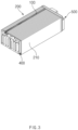
- FIG. 3 is a perspective view showing main parts of a battery pack in which a printed circuit board for a battery pack capable of measuring temperature according to an embodiment of the present invention is utilized.
- the battery pack 1000 in which a printed circuit board for a battery pack capable of measuring temperature according to an embodiment of the present invention is utilized, may include a cell stack 200 in which a plurality of secondary batteries 210 are stacked, busbar frames 400 and 500 which electrically connect electrode leads 20 of the plurality of secondary batteries 210 to each other, and a pack case 300 which accommodates therein the cell stack 200 and the busbar frames 400 and 500. Also, the battery pack 1000 may further include end plates 600 and 700 for covering openings on both sides of the pack case 300.
- the printed circuit board for a battery pack capable of measuring temperature according to an embodiment of the present invention may include, for example, a flexible printed circuit board (FPCB) for connecting the plurality of busbar frames 400 and 500 to each other.
- FPCB flexible printed circuit board
- the printed circuit board for a battery pack capable of measuring temperature according to an embodiment of the present invention is not necessarily limited to a printed circuit board for connecting the busbar frames 400 and 500.
- the printed circuit board may be applied in any place thereof.
- the cell stack 200 may form a stack in which the plurality of secondary batteries 210 containing an electrolyte are stacked.
- Each of the secondary batteries 210 may include an electrode assembly, an electrolyte, and a pouch that accommodates the electrode assembly and electrolyte therein.
- the electrode assembly serves as a power generating element capable of charging and discharging, and may be configured by alternately stacking electrodes and separators.
- the electrodes include positive electrodes and the negative electrodes, and thus, the positive electrodes, the separators, and the negative electrodes may be alternately stacked.
- the separators separate and electrically insulate the positive electrodes and the negative electrodes from each other.
- One side of the secondary battery 210 may be connected to an electrode of the electrode assembly, and the other side thereof may further include electrode leads 211 extending to the outside of the pouch.
- the electrode leads 211 may include positive electrode leads connected to the positive electrodes and negative electrode leads connected to the negative electrodes.
- the film 110 may be provided in the form of a sheet.
- the film 110 may include an insulating material and a flexible material.
- the film 110 may include, for example, resin.
- the film 110 may specifically include, for example, synthetic resin.
- the film 110 may provide a substrate on which the conductive pattern 130 and the temperature element 140 are printed.
- the conductive pattern 130 may be formed on the first portion of the film 110.
- the conductive pattern 130 may be positioned on the first portion of one surface of the film 110.
- the conductive pattern 130 includes an ink-type material and may be provided in the form printed on the film 110.
- the conductive pattern 130 may be printed on the first portion of the one surface of the film 110.
- the conductive pattern 130 may include a silver (Ag) material.
- the conductive pattern 130 may include, for example, an electrically conductive circuit pattern.
- the temperature element 140 is formed on the second portion of the film 110 and may measure the temperature inside the battery pack 1000.
- the temperature element 140 may be positioned on the second portion of one surface of the film 110.
- the temperature element may be positioned between conductive patterns 130.
- the temperature element may be provided in contact with the conductive patterns 130.
- the conductive pattern 130 may be in contact with, for example, both surfaces of the temperature element.
- the temperature element 140 includes an ink-type material and may be provided in the form printed on the film 110.
- the temperature element 140 may be printed on the second portion of the one surface of the film 110.
- the temperature element 140 may form, for example, a pattern.
- the temperature element may include a thermistor.
- the thermistor may include an element, of which an electrical resistance value varies according to temperature. Accordingly, the temperature may be measured by the resistance value of the temperature element.
- the temperature element may include a nickel oxide (NiO) material.
- the cover layer 150 may cover both the conductive pattern 130 and the temperature element 140.
- the cover layer 150 may be positioned on one surface of the film 110 and applied to both the conductive pattern 130 and the temperature element 140 printed on the one surface of the film 110.
- cover layer 150 may include an insulating material.
- cover layer 150 may include, for example, resin.
- the binder 120 may bond the conductive pattern 130 and the temperature element 140 to the film 110.
- the binder 120 may be positioned between the film 110 and both the conductive pattern 130 and the temperature element 140 to form a layer.
- a method for manufacturing a printed circuit board for a battery pack capable of measuring temperature according to an embodiment of the present invention is described below.
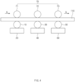
- FIG. 4 is a front view conceptually showing a method for manufacturing a printed circuit board for a battery pack capable of measuring temperature according to an embodiment of the present invention.
- the method for manufacturing a printed circuit board provided in a battery pack 1000 that includes a plurality of secondary batteries 210 the method including: a film preparation operation of preparing a film 110; a conductive pattern formation operation of forming a conductive pattern 130 on a first portion of the prepared film 110; and a temperature element formation operation of forming a temperature element 140, which measures the temperature inside the battery pack 1000, on a second portion of the film 110 after the conductive pattern 130 is formed.
- the method for manufacturing a printed circuit board for a battery pack capable of measuring temperature includes a cover layer formation operation and a binder coating operation.
- the method for manufacturing a printed circuit board for a battery pack capable of measuring temperature relates to a method for manufacturing the printed circuit board 100 for a battery pack capable of measuring temperature according to the embodiment described above.
- this embodiment is described with a focus on differences from the above embodiment, and repeated descriptions are omitted or briefly described.
- the film 110 may be prepared during the film preparation operation.
- the film 110 in the form of a sheet may be prepared during the film preparation operation.
- the film 110 may include an insulating material and a flexible material.
- the film 110 may include, for example, resin.
- the film 110 may specifically include, for example, synthetic resin.
- guide rollers 70 may include a first guide roller 71, a second guide roller 72, and a third guide roller 73.
- the binder coating operation is performed after the film preparation operation and before the conductive pattern formation operation, and a binder 120 may be applied on the film 110 so as to bond a conductive pattern 130 and a temperature element 140 to the film 110.
- the binder 120 may be positioned between the film 110 and both the conductive pattern 130 and the temperature element 140 to form a layer.
- a binder ink accommodated in a binder pool 20 may be applied to one surface of the film 110 by a binder roller 10.
- the other surface of the film 110 and the first guide roller 71 are in contact with each other, and the first guide roller 71 may guide the movement of the film 110.
- the first guide roller 71 may face the binder roller 10 with the film 110 therebetween.
- the conductive pattern 130 may be formed on a first portion of the prepared film 110.
- the conductive pattern 130 may be positioned on the first portion of one surface of the film 110.
- the conductive pattern 130 may be printed on the film 110 with conductive pattern ink.
- the conductive pattern 130 may include a silver (Ag) material.
- silver (Ag) ink accommodated in a conductive pattern pool 40 may be applied, through printing, on the first portion of the one surface of the film 110 by a conductive pattern roller 30.
- the silver (Ag) ink may be applied through printing, by the conductive pattern roller 30, on the first portion of the one surface of the film 110 that has been coated with the binder 120.
- the conductive pattern roller 30 may have, as a roll-type print frame, a pattern frame that is formed along the outer circumferential surface and corresponds to the conductive pattern 130.
- the conductive pattern 130 may be directly nano-printed on the film by the conductive pattern roller 30 using the silver (Ag) ink. Accordingly, the conductive pattern 130 does not protrude, and thus, it is possible to prevent a structural problem due to the protrusion.
- the conductive pattern 130 includes the silver (Ag) material having excellent water resistance, and thus, it is possible to prevent an insulation problem from occurring due to being vulnerable to moisture.
- the other surface of the film 110 and the second guide roller 72 are in contact with each other, and the second guide roller 72 may guide the movement of the film 110.
- the second guide roller 72 may face the conductive pattern roller 30 with the film 110 therebetween.
- FIG. 5 is a cross-sectional view showing an operation of forming a temperature element in a method for manufacturing a printed circuit board for a battery pack capable of measuring temperature according to an embodiment of the present invention.
- the temperature element 140 which measures the temperature inside the battery pack 1000, may be formed on the second portion of the film 110 after the conductive pattern 130 is formed.
- the temperature element 140 may be positioned on the second portion of the one surface of the film 110.
- the temperature element 140 may be printed on the film 110 with temperature element ink.
- the temperature element may include a thermistor.
- the temperature element may include a nickel oxide (NiO) material.
- nickel oxide (NiO) ink accommodated in a temperature element pool 60 may be applied, through printing, on the second portion of the one surface of the film 110 by a temperature element roller 50.
- the nickel oxide (NiO) ink may be applied through printing, by the temperature element roller 50, on the second portion of the one surface of the film 110 that has been coated with the binder 120.
- the temperature element roller 50 may have, as a roll-type print frame, a pattern frame that is formed along the outer circumferential surface and corresponds to the pattern of the temperature element 140.
- the pattern of the temperature element 140 may be directly nano-printed on the film 110 by the temperature element roller 50 using the nickel oxide (NiO) ink. Accordingly, the pattern of the temperature element 140 does not protrude, and thus, it is possible to prevent a structural problem due to the protrusion. In addition, a surface mounted technology (SMT) process for structurally mounting the temperature element 140 is not used, and thus, manufacturing may be facilitated. Furthermore, the temperature element 140 includes the nickel oxide (NiO), which is easy to measure temperature, and thus, the temperature inside the battery pack 1000 may be easily and accurately measured.
- NiO nickel oxide
- the third guide roller 73 may guide the movement of the film 110.
- the third guide roller 73 may face the temperature element roller 50 with the film 110 therebetween.
- FIG. 6 is a front view showing an operation of forming a cover layer in a method for manufacturing a printed circuit board for a battery pack capable of measuring temperature according to an embodiment of the present invention.
- the cover layer formation operation is performed after the temperature element formation operation, and a cover layer 150 for covering both the conductive pattern 130 and the temperature element 140 may be formed.
- the cover layer 150 may be positioned on one surface of the film 110 and applied to both the conductive pattern 130 and the temperature element 140 printed on the one surface of the film 110.
- the cover layer 150 may include an insulating material. Also, the cover layer 150 may include, for example, resin.
- the cover layer 150 may be formed by laminating a cover sheet on one surface of the film 110 by a lamination roller 80.
- the lamination roller 80 may include an upper lamination roller 81 and a lower lamination roller 82.
- the cover sheet and the film 110, on which the conductive pattern 130 and the temperature element 140 are printed are allowed to pass between the upper lamination roller 81 and the lower lamination roller 82 and may be bonded to each other by applying heat and pressure thereto.
Landscapes
- Engineering & Computer Science (AREA)
- Microelectronics & Electronic Packaging (AREA)
- Chemical & Material Sciences (AREA)
- Manufacturing & Machinery (AREA)
- Chemical Kinetics & Catalysis (AREA)
- Electrochemistry (AREA)
- General Chemical & Material Sciences (AREA)
- Physics & Mathematics (AREA)
- Electromagnetism (AREA)
- General Physics & Mathematics (AREA)
- Dispersion Chemistry (AREA)
- Life Sciences & Earth Sciences (AREA)
- Materials Engineering (AREA)
- Wood Science & Technology (AREA)
- Organic Chemistry (AREA)
- Battery Mounting, Suspending (AREA)
Abstract
Description
- The present application claims the benefit of the priority of
Korean Patent Application No. 2022-0013746, filed on January 28, 2022 - The present invention relates to a printed circuit board for a battery pack capable of measuring temperature and a method for manufacturing same.
- Secondary batteries, unlike primary batteries, can be recharged and have been extensively researched and developed in recent years due to small sizes and high capacities thereof. As technology development and demands for mobile devices increase, the demands for secondary batteries as energy sources are rapidly increasing.
- Secondary batteries are classified into coin-type batteries, cylindrical batteries, prismatic batteries, and pouch-type batteries depending on shapes of battery cases. In such a secondary battery, an electrode assembly installed inside a battery case serves as a chargeable and dischargeable power generating element that has a structure in which electrodes and separators are stacked.
- The secondary batteries are attracting much attention as energy sources for power devices, such as electric bicycles, electric vehicles, and hybrid electric vehicles, as well as mobile devices, such as mobile phones, digital cameras, and laptop computers.
- A small-sized battery pack, in which one battery cell is packed, is used in small devices, such as mobile phones and cameras. However, a medium- or large-sized battery pack, in which two or more battery cells connected in parallel and/or in series are packed, is used in medium- or large-sized devices, such as laptop computers and electric vehicles. Accordingly, the number of battery cells included in the battery pack may be variously set depending on required output voltages or charge/discharge capacities.
- Meanwhile, when constituting a battery pack by connecting a plurality of battery cells in series/in parallel, it is common to first constitute a battery module including at least one battery cell. Subsequently, a battery pack is constituted by using the at least one battery module and adding other components. The number of battery modules included in the battery pack or the number of battery cells included in the battery module may be variously set depending on required output voltages or charge/discharge capacities. The battery module configured as described above includes a plurality of battery cells stacked on each other and a busbar electrically connecting electrode leads of the plurality of battery cells.
- In order to prevent the performance of the battery pack from deteriorating, a battery temperature management system is mounted on a vehicle. In addition, sensing is required to manage the temperature of the battery pack, and a temperature sensor for the sensing is required.
- One aspect of the present invention is to provide a printed circuit board for a battery pack, capable of measuring temperature and facilitating measuring the temperature of a battery pack, and a method for manufacturing same.
- An embodiment of the present invention provides a printed circuit board for a battery pack, capable of measuring temperature and provided in a battery pack that includes a plurality of secondary batteries, the printed circuit board including: a film; a conductive pattern provided on a first portion of the film; and a temperature element provided on a second portion of the film and measuring the temperature inside the battery pack.
- An embodiment of the present invention provides a method for manufacturing a printed circuit board for a battery pack, capable of measuring temperature and provided in a battery pack that includes a plurality of secondary batteries, the method including: a film preparation operation of preparing a film; a conductive pattern formation operation of forming a conductive pattern on a first portion of the prepared film; and a temperature element formation operation of forming a temperature element, which measures the temperature inside the battery pack, on a second portion of the film after the conductive pattern is formed.
- According to the present invention, a temperature element is provided on a printed circuit board provided in a battery pack, and thus, the temperature of the battery pack may be easily measured.
-
-
FIG. 1 is a cross-sectional view showing a printed circuit board for a battery pack capable of measuring temperature according to an embodiment of the present invention. -
FIG. 2 is an exploded perspective view showing a battery pack in which a printed circuit board for a battery pack capable of measuring temperature according to an embodiment of the present invention is utilized. -
FIG. 3 is a perspective view showing main parts of a battery pack in which a printed circuit board for a battery pack capable of measuring temperature according to an embodiment of the present invention is utilized. -
FIG. 4 is a front view conceptually showing a method for manufacturing a printed circuit board for a battery pack capable of measuring temperature according to an embodiment of the present invention. -
FIG. 5 is a cross-sectional view showing an operation of forming a temperature element in a method for manufacturing a printed circuit board for a battery pack capable of measuring temperature according to an embodiment of the present invention. -
FIG. 6 is a front view showing an operation of forming a cover layer in a method for manufacturing a printed circuit board for a battery pack capable of measuring temperature according to an embodiment of the present invention. - The objects, specific advantages, and novel features of the present invention will be more clearly understood from the following detailed description and preferred embodiments taken in conjunction with the accompanying drawings. In the specification, when reference numerals are given to elements in each drawing, it should be noted that the same elements will be designated by the same reference numerals if possible although they are shown in different drawings. Also, the present invention may be embodied in various different forms, and is not limited to the embodiments described herein. In addition, in describing the present invention, detailed descriptions related to well-known functions are omitted so as not to unnecessarily obscure subject matters of the present invention.
-
FIG. 1 is a cross-sectional view showing a printed circuit board for a battery pack capable of measuring temperature according to an embodiment of the present invention, andFIG. 2 is an exploded perspective view showing a battery pack in which a printed circuit board for a battery pack capable of measuring temperature according to an embodiment of the present invention is utilized. - Referring to
FIGS. 1 and2 , a printedcircuit board 100 for a battery pack capable of measuring temperature according to an embodiment of the present invention is provided in abattery pack 1000 that includes a plurality ofsecondary batteries 210, and the printedcircuit board 100 includes afilm 110, aconductive pattern 130 provided on a first portion of thefilm 110, and atemperature element 140 provided on a second portion of thefilm 110 and measuring the temperature inside thebattery pack 1000. The printedcircuit board 100 for a battery pack capable of measuring temperature according to an embodiment of the present invention may further include acover layer 150 and abinder 120. -
FIG. 3 is a perspective view showing main parts of a battery pack in which a printed circuit board for a battery pack capable of measuring temperature according to an embodiment of the present invention is utilized. - In more detail, referring to
FIGS. 1 to 3 , thebattery pack 1000, in which a printed circuit board for a battery pack capable of measuring temperature according to an embodiment of the present invention is utilized, may include acell stack 200 in which a plurality ofsecondary batteries 210 are stacked,busbar frames secondary batteries 210 to each other, and apack case 300 which accommodates therein thecell stack 200 and thebusbar frames battery pack 1000 may further includeend plates pack case 300. - The printed circuit board for a battery pack capable of measuring temperature according to an embodiment of the present invention may include, for example, a flexible printed circuit board (FPCB) for connecting the plurality of
busbar frames busbar frames battery pack 1000, the printed circuit board may be applied in any place thereof. - The
cell stack 200 may form a stack in which the plurality ofsecondary batteries 210 containing an electrolyte are stacked. - Each of the
secondary batteries 210 may include an electrode assembly, an electrolyte, and a pouch that accommodates the electrode assembly and electrolyte therein. - The electrode assembly serves as a power generating element capable of charging and discharging, and may be configured by alternately stacking electrodes and separators. Here, the electrodes include positive electrodes and the negative electrodes, and thus, the positive electrodes, the separators, and the negative electrodes may be alternately stacked. Here, the separators separate and electrically insulate the positive electrodes and the negative electrodes from each other.
- One side of the
secondary battery 210 may be connected to an electrode of the electrode assembly, and the other side thereof may further include electrode leads 211 extending to the outside of the pouch. - The electrode leads 211 may include positive electrode leads connected to the positive electrodes and negative electrode leads connected to the negative electrodes.
- Referring to
FIG. 1 , thefilm 110 may be provided in the form of a sheet. - Also, the
film 110 may include an insulating material and a flexible material. Herein, thefilm 110 may include, for example, resin. Here, thefilm 110 may specifically include, for example, synthetic resin. - In addition, the
film 110 may provide a substrate on which theconductive pattern 130 and thetemperature element 140 are printed. - The
conductive pattern 130 may be formed on the first portion of thefilm 110. Here, theconductive pattern 130 may be positioned on the first portion of one surface of thefilm 110. - In addition, the
conductive pattern 130 includes an ink-type material and may be provided in the form printed on thefilm 110. Here, theconductive pattern 130 may be printed on the first portion of the one surface of thefilm 110. - Also, the
conductive pattern 130 may include a silver (Ag) material. - Also, the
conductive pattern 130 may include, for example, an electrically conductive circuit pattern. - The
temperature element 140 is formed on the second portion of thefilm 110 and may measure the temperature inside thebattery pack 1000. Here, thetemperature element 140 may be positioned on the second portion of one surface of thefilm 110. - Also, the temperature element may be positioned between
conductive patterns 130. Here, the temperature element may be provided in contact with theconductive patterns 130. Here, theconductive pattern 130 may be in contact with, for example, both surfaces of the temperature element. - Also, the
temperature element 140 includes an ink-type material and may be provided in the form printed on thefilm 110. Here, thetemperature element 140 may be printed on the second portion of the one surface of thefilm 110. Here, thetemperature element 140 may form, for example, a pattern. - In addition, the temperature element may include a thermistor. The thermistor may include an element, of which an electrical resistance value varies according to temperature. Accordingly, the temperature may be measured by the resistance value of the temperature element.
- Here, the temperature element may include a nickel oxide (NiO) material.
- The
cover layer 150 may cover both theconductive pattern 130 and thetemperature element 140. Here, thecover layer 150 may be positioned on one surface of thefilm 110 and applied to both theconductive pattern 130 and thetemperature element 140 printed on the one surface of thefilm 110. - In addition, the
cover layer 150 may include an insulating material. - Also, the
cover layer 150 may include, for example, resin. - The
binder 120 may bond theconductive pattern 130 and thetemperature element 140 to thefilm 110. - In addition, the
binder 120 may be positioned between thefilm 110 and both theconductive pattern 130 and thetemperature element 140 to form a layer. - A method for manufacturing a printed circuit board for a battery pack capable of measuring temperature according to an embodiment of the present invention is described below.
-
FIG. 4 is a front view conceptually showing a method for manufacturing a printed circuit board for a battery pack capable of measuring temperature according to an embodiment of the present invention. - Referring to
FIGS. 1 and4 , during a secondary battery manufacturing method according to an embodiment of the present invention, provided is the method for manufacturing a printed circuit board provided in abattery pack 1000 that includes a plurality ofsecondary batteries 210, the method including: a film preparation operation of preparing afilm 110; a conductive pattern formation operation of forming aconductive pattern 130 on a first portion of theprepared film 110; and a temperature element formation operation of forming atemperature element 140, which measures the temperature inside thebattery pack 1000, on a second portion of thefilm 110 after theconductive pattern 130 is formed. Also, the method for manufacturing a printed circuit board for a battery pack capable of measuring temperature according to an embodiment of the present invention includes a cover layer formation operation and a binder coating operation. - The method for manufacturing a printed circuit board for a battery pack capable of measuring temperature according to an embodiment of the present invention relates to a method for manufacturing the printed
circuit board 100 for a battery pack capable of measuring temperature according to the embodiment described above. Thus, this embodiment is described with a focus on differences from the above embodiment, and repeated descriptions are omitted or briefly described. - More specifically, the
film 110 may be prepared during the film preparation operation. Here, thefilm 110 in the form of a sheet may be prepared during the film preparation operation. - Herein, the
film 110 may include an insulating material and a flexible material. Herein, thefilm 110 may include, for example, resin. Here, thefilm 110 may specifically include, for example, synthetic resin. - Meanwhile, the
film 110 is moved in a direction G in which the binder coating operation, the conductive pattern formation operation, the temperature element formation operation, and the cover layer formation operation are performed, and the movement thereof may be guided by guide rollers. Here, guiderollers 70 may include afirst guide roller 71, asecond guide roller 72, and athird guide roller 73. - Referring to
FIGS. 1 and4 , the binder coating operation is performed after the film preparation operation and before the conductive pattern formation operation, and abinder 120 may be applied on thefilm 110 so as to bond aconductive pattern 130 and atemperature element 140 to thefilm 110. - Also, during the binder coating operation, the
binder 120 may be positioned between thefilm 110 and both theconductive pattern 130 and thetemperature element 140 to form a layer. - Also, during the binder coating operation, a binder ink accommodated in a
binder pool 20 may be applied to one surface of thefilm 110 by abinder roller 10. - Meanwhile, during the binder coating operation, the other surface of the
film 110 and thefirst guide roller 71 are in contact with each other, and thefirst guide roller 71 may guide the movement of thefilm 110. Here, thefirst guide roller 71 may face thebinder roller 10 with thefilm 110 therebetween. - During the conductive pattern formation operation, the
conductive pattern 130 may be formed on a first portion of theprepared film 110. Here, during the conductive pattern formation operation, theconductive pattern 130 may be positioned on the first portion of one surface of thefilm 110. - Also, during the conductive pattern formation operation, the
conductive pattern 130 may be printed on thefilm 110 with conductive pattern ink. Here, theconductive pattern 130 may include a silver (Ag) material. - Also, during the conductive pattern formation operation, silver (Ag) ink accommodated in a
conductive pattern pool 40 may be applied, through printing, on the first portion of the one surface of thefilm 110 by aconductive pattern roller 30. Here, during the conductive pattern formation operation, the silver (Ag) ink may be applied through printing, by theconductive pattern roller 30, on the first portion of the one surface of thefilm 110 that has been coated with thebinder 120. - The
conductive pattern roller 30 may have, as a roll-type print frame, a pattern frame that is formed along the outer circumferential surface and corresponds to theconductive pattern 130. - Therefore, during the conductive pattern formation operation, the
conductive pattern 130 may be directly nano-printed on the film by theconductive pattern roller 30 using the silver (Ag) ink. Accordingly, theconductive pattern 130 does not protrude, and thus, it is possible to prevent a structural problem due to the protrusion. In addition, theconductive pattern 130 includes the silver (Ag) material having excellent water resistance, and thus, it is possible to prevent an insulation problem from occurring due to being vulnerable to moisture. - Meanwhile, during the conductive pattern formation operation, the other surface of the
film 110 and thesecond guide roller 72 are in contact with each other, and thesecond guide roller 72 may guide the movement of thefilm 110. Here, thesecond guide roller 72 may face theconductive pattern roller 30 with thefilm 110 therebetween. -
FIG. 5 is a cross-sectional view showing an operation of forming a temperature element in a method for manufacturing a printed circuit board for a battery pack capable of measuring temperature according to an embodiment of the present invention. - Referring to
FIGS. 4 and5 , during the temperature element formation operation, thetemperature element 140, which measures the temperature inside thebattery pack 1000, may be formed on the second portion of thefilm 110 after theconductive pattern 130 is formed. Here, during the temperature element formation operation, thetemperature element 140 may be positioned on the second portion of the one surface of thefilm 110. - Also, during the temperature element formation operation, the
temperature element 140 may be printed on thefilm 110 with temperature element ink. - In addition, the temperature element may include a thermistor. Here, the temperature element may include a nickel oxide (NiO) material.
- Also, during the temperature element formation operation, nickel oxide (NiO) ink accommodated in a
temperature element pool 60 may be applied, through printing, on the second portion of the one surface of thefilm 110 by atemperature element roller 50. Here, during the temperature element formation operation, the nickel oxide (NiO) ink may be applied through printing, by thetemperature element roller 50, on the second portion of the one surface of thefilm 110 that has been coated with thebinder 120. - The
temperature element roller 50 may have, as a roll-type print frame, a pattern frame that is formed along the outer circumferential surface and corresponds to the pattern of thetemperature element 140. - Therefore, during the temperature element formation operation, the pattern of the
temperature element 140 may be directly nano-printed on thefilm 110 by thetemperature element roller 50 using the nickel oxide (NiO) ink. Accordingly, the pattern of thetemperature element 140 does not protrude, and thus, it is possible to prevent a structural problem due to the protrusion. In addition, a surface mounted technology (SMT) process for structurally mounting thetemperature element 140 is not used, and thus, manufacturing may be facilitated. Furthermore, thetemperature element 140 includes the nickel oxide (NiO), which is easy to measure temperature, and thus, the temperature inside thebattery pack 1000 may be easily and accurately measured. - Meanwhile, during the temperature element formation operation, the other surface of the
film 110 and thethird guide roller 73 are in contact with each other, and thethird guide roller 73 may guide the movement of thefilm 110. Here, thethird guide roller 73 may face thetemperature element roller 50 with thefilm 110 therebetween. -
FIG. 6 is a front view showing an operation of forming a cover layer in a method for manufacturing a printed circuit board for a battery pack capable of measuring temperature according to an embodiment of the present invention. - Referring to
FIGS. 1 ,4 , and6 , the cover layer formation operation is performed after the temperature element formation operation, and acover layer 150 for covering both theconductive pattern 130 and thetemperature element 140 may be formed. - Here, during the cover layer formation operation, the
cover layer 150 may be positioned on one surface of thefilm 110 and applied to both theconductive pattern 130 and thetemperature element 140 printed on the one surface of thefilm 110. - The
cover layer 150 may include an insulating material. Also, thecover layer 150 may include, for example, resin. - In addition, during the cover layer formation operation, the
cover layer 150 may be formed by laminating a cover sheet on one surface of thefilm 110 by alamination roller 80. - The
lamination roller 80 may include anupper lamination roller 81 and alower lamination roller 82. Here, during the cover layer formation operation, the cover sheet and thefilm 110, on which theconductive pattern 130 and thetemperature element 140 are printed, are allowed to pass between theupper lamination roller 81 and thelower lamination roller 82 and may be bonded to each other by applying heat and pressure thereto. - Although the present invention has been described in detail through the specific embodiments, these are intended to specifically describe the present invention, and the present invention is not limited thereto. Various modifications can be made within the technical idea of the present invention by those skilled in the art.
- Also, the specific protection scope of the invention can become apparent from the appended claims.
-
- 10:
- Binder roller
- 20:
- Binder pool
- 30:
- Conductive pattern roller
- 40:
- Conductive pattern pool
- 50:
- Temperature element roller
- 60:
- Temperature element pool
- 70:
- Guide roller
- 71:
- First guide roller
- 72:
- Second guide roller
- 73:
- Third guide roller
- 80:
- Lamination roller
- 81:
- Upper lamination roller
- 82:
- Lower lamination roller
- 100:
- Printed circuit board
- 110:
- Film
- 120:
- Binder
- 130:
- Conductive pattern
- 140:
- Temperature element
- 150:
- Cover layer
- 200:
- Cell stack
- 210:
- Secondary battery
- 211:
- Electrode lead
- 300:
- Pack case
- 400, 500:
- Busbar frame
- 600, 700:
- End plate
- 1000:
- Battery pack
Claims (15)
- A printed circuit board for a battery pack, capable of measuring temperature and provided in a battery pack that comprises a plurality of secondary batteries, the printed circuit board comprising:a film;a conductive pattern provided on a first portion of the film; anda temperature element provided on a second portion of the film and measuring the temperature inside the battery pack.
- The printed circuit board of claim 1, wherein the conductive pattern is positioned on the first portion of one surface of the film, and
the temperature element is positioned on the second portion of the one surface of the film. - The printed circuit board of claim 1 or 2, further comprising a cover layer configured to cover the conductive pattern and the temperature element.
- The printed circuit board of claim 1, wherein the conductive pattern comprises a silver (Ag) material.
- The printed circuit board of claim 1, wherein the temperature element comprises a thermistor.
- The printed circuit board of claim 5, wherein the conductive pattern comprises an ink-type material, and the temperature element comprises an ink-type thermistor, and thus, the conductive pattern and the temperature element are provided in the form printed on the film.
- The printed circuit board of claim 6, wherein the temperature element comprises a nickel oxide (NiO) material.
- The printed circuit board of claim 1, further comprising a binder configured to bond the conductive pattern and the temperature element to the film.
- A method for manufacturing a printed circuit board, which is provided in a battery pack that comprises a plurality of secondary batteries, the method comprising:a film preparation operation of preparing a film;a conductive pattern formation operation of forming a conductive pattern on a first portion of the prepared film; anda temperature element formation operation of forming a temperature element, which measures the temperature inside the battery pack, on a second portion of the film after the conductive pattern is formed.
- The method of claim 9, wherein the conductive pattern is positioned on the first portion of one surface of the film during the conductive pattern formation operation, and
the temperature element is positioned on the second portion of the one surface of the film during the temperature element formation operation. - The method of claim 9, further comprising, after the temperature element formation operation, a cover layer formation operation of forming a cover layer configured to cover the conductive pattern and the temperature element.
- The method of claim 9, wherein the conductive pattern is printed on the film with conductive pattern ink during the conductive pattern formation operation, and
the temperature element is printed on the film with temperature element ink during the temperature element formation operation. - The method of claim 9, wherein the conductive pattern comprises a silver (Ag) material.
- The method of claim 9, wherein the temperature element comprises a nickel oxide (NiO) material.
- The method of claim 9, further comprising, after the film preparation operation and before the conductive pattern formation operation, a binder coating operation of coating the film with a binder configured to bond the conductive pattern and the temperature element to the film.
Applications Claiming Priority (2)
| Application Number | Priority Date | Filing Date | Title |
|---|---|---|---|
| KR1020220013746A KR102790200B1 (en) | 2022-01-28 | 2022-01-28 | Printed circuit board for battery pack capable of measuring temperature and manufacturing method therefor |
| PCT/KR2023/001066 WO2023146242A1 (en) | 2022-01-28 | 2023-01-20 | Battery pack printed circuit board capable of measuring temperature, and manufacturing method therefor |
Publications (2)
| Publication Number | Publication Date |
|---|---|
| EP4472361A1 true EP4472361A1 (en) | 2024-12-04 |
| EP4472361A4 EP4472361A4 (en) | 2025-05-21 |
Family
ID=87471926
Family Applications (1)
| Application Number | Title | Priority Date | Filing Date |
|---|---|---|---|
| EP23747283.2A Pending EP4472361A4 (en) | 2022-01-28 | 2023-01-20 | Battery pack circuit board for measuring temperature and manufacturing process therefor |
Country Status (6)
| Country | Link |
|---|---|
| US (1) | US20250227847A1 (en) |
| EP (1) | EP4472361A4 (en) |
| JP (1) | JP2025502430A (en) |
| KR (1) | KR102790200B1 (en) |
| CN (1) | CN118592095A (en) |
| WO (1) | WO2023146242A1 (en) |
Family Cites Families (15)
| Publication number | Priority date | Publication date | Assignee | Title |
|---|---|---|---|---|
| DE2856888A1 (en) * | 1978-12-30 | 1980-07-17 | Licentia Gmbh | Printed circuit boards - mfd by applying elastic adhesive coating for conductor tracks and soldering tags |
| US6152597A (en) * | 1997-06-27 | 2000-11-28 | Potega; Patrick H. | Apparatus for monitoring temperature of a power source |
| KR100570726B1 (en) * | 2005-07-22 | 2006-04-12 | 주식회사 린포스 | Super low temperature super battery pack with excellent temperature compensation |
| EP2479835B1 (en) * | 2009-09-15 | 2017-01-11 | LG Chem, Ltd. | Battery module having a temperature sensor installed thereon, and medium or large battery pack including same |
| KR101312569B1 (en) * | 2012-02-29 | 2013-10-14 | 유홍근 | Film type temperature sensor |
| KR20160091726A (en) * | 2015-01-26 | 2016-08-03 | 엘지이노텍 주식회사 | sensing chip and method for making the sensing chip |
| CN110494805A (en) * | 2017-03-13 | 2019-11-22 | 伊斯曼柯达公司 | Silver-containing compositions and uses containing cellulosic polymers |
| KR20190009977A (en) * | 2017-07-20 | 2019-01-30 | 삼성에스디아이 주식회사 | Battery pack |
| KR102327049B1 (en) * | 2017-11-06 | 2021-11-15 | 주식회사 엘지에너지솔루션 | Battery module |
| US11085833B2 (en) * | 2018-10-31 | 2021-08-10 | Xerox Corporation | Temperature sensor ink composition with metal oxide nanoparticles |
| KR102306042B1 (en) * | 2018-12-11 | 2021-09-27 | 주식회사 엘지에너지솔루션 | FPCB assembly for battery module and a method for manufacturing FPCB assembly and a battery module including the same |
| KR102779080B1 (en) * | 2019-07-03 | 2025-03-11 | 주식회사 엘지에너지솔루션 | Secondary battery, method of manufacturing the same and battery module including the same |
| US12160024B2 (en) * | 2019-07-05 | 2024-12-03 | Autonetworks Technologies, Ltd. | Wiring module |
| KR102161215B1 (en) * | 2019-11-06 | 2020-09-29 | 고려전자주식회사 | Temperature Sensor for Battery Module and Battery Module including the same |
| KR102837601B1 (en) * | 2020-03-05 | 2025-07-22 | 주식회사 엘지에너지솔루션 | Battery module and battery pack including the same |
-
2022
- 2022-01-28 KR KR1020220013746A patent/KR102790200B1/en active Active
-
2023
- 2023-01-20 US US18/833,002 patent/US20250227847A1/en active Pending
- 2023-01-20 JP JP2024543165A patent/JP2025502430A/en active Pending
- 2023-01-20 EP EP23747283.2A patent/EP4472361A4/en active Pending
- 2023-01-20 CN CN202380018564.5A patent/CN118592095A/en active Pending
- 2023-01-20 WO PCT/KR2023/001066 patent/WO2023146242A1/en not_active Ceased
Also Published As
| Publication number | Publication date |
|---|---|
| EP4472361A4 (en) | 2025-05-21 |
| WO2023146242A1 (en) | 2023-08-03 |
| KR102790200B1 (en) | 2025-04-03 |
| US20250227847A1 (en) | 2025-07-10 |
| KR20230116599A (en) | 2023-08-04 |
| CN118592095A (en) | 2024-09-03 |
| JP2025502430A (en) | 2025-01-24 |
Similar Documents
| Publication | Publication Date | Title |
|---|---|---|
| US9077027B2 (en) | Electrode assembly and secondary battery using the same | |
| US7427453B2 (en) | Pouched lithium secondary battery | |
| JP4628682B2 (en) | Battery unit and lithium secondary battery using the same | |
| KR101042132B1 (en) | Case for high output lithium secondary battery | |
| JP7221122B2 (en) | Battery cell electrode assembly manufacturing method and battery cell | |
| EP2405507B1 (en) | Rechargeable battery | |
| WO2019107795A1 (en) | Battery pack | |
| WO2014081193A1 (en) | Secondary battery module | |
| KR101984314B1 (en) | Secondary battery | |
| CN101167203B (en) | Battery | |
| KR102332343B1 (en) | The Battery Module | |
| EP2827406B1 (en) | Rechargeable battery | |
| JP7098189B2 (en) | Secondary battery and battery module | |
| CN111194488B (en) | Battery pack and label attachment method thereof | |
| US20120028082A1 (en) | Battery pack | |
| US20250227847A1 (en) | Printed Circuit Board For Battery Pack Capable Of Measuring Temperature And Method For Manufacturing Same | |
| KR20190055994A (en) | Secondary battery | |
| EP4468446A1 (en) | Battery pack | |
| EP4184682A1 (en) | Battery module and battery pack including same | |
| CN114447443B (en) | Electrochemical device, method for manufacturing electrochemical device, and electrical equipment | |
| KR20190060963A (en) | Secondary battery | |
| KR100580767B1 (en) | Pouch Type Lithium-ion Polymer Battery | |
| CN114552136B (en) | Power supply assembly and manufacturing method thereof | |
| CN222581445U (en) | Batteries, charging and discharging modules and electronic equipment | |
| CN102074675B (en) | Protection circuit module for secondary batteries and battery pack provided with protection circuit module |
Legal Events
| Date | Code | Title | Description |
|---|---|---|---|
| STAA | Information on the status of an ep patent application or granted ep patent |
Free format text: STATUS: THE INTERNATIONAL PUBLICATION HAS BEEN MADE |
|
| PUAI | Public reference made under article 153(3) epc to a published international application that has entered the european phase |
Free format text: ORIGINAL CODE: 0009012 |
|
| STAA | Information on the status of an ep patent application or granted ep patent |
Free format text: STATUS: REQUEST FOR EXAMINATION WAS MADE |
|
| 17P | Request for examination filed |
Effective date: 20240709 |
|
| AK | Designated contracting states |
Kind code of ref document: A1 Designated state(s): AL AT BE BG CH CY CZ DE DK EE ES FI FR GB GR HR HU IE IS IT LI LT LU LV MC ME MK MT NL NO PL PT RO RS SE SI SK SM TR |
|
| DAV | Request for validation of the european patent (deleted) | ||
| DAX | Request for extension of the european patent (deleted) | ||
| A4 | Supplementary search report drawn up and despatched |
Effective date: 20250417 |
|
| RIC1 | Information provided on ipc code assigned before grant |
Ipc: C09D 11/52 20140101ALI20250411BHEP Ipc: H01M 10/48 20060101ALI20250411BHEP Ipc: G01K 13/00 20210101ALI20250411BHEP Ipc: G01K 7/16 20060101ALI20250411BHEP Ipc: G01K 1/14 20210101ALI20250411BHEP Ipc: H01M 10/60 20140101ALI20250411BHEP Ipc: H01C 7/00 20060101ALI20250411BHEP Ipc: H05K 1/09 20060101ALI20250411BHEP Ipc: H05K 1/16 20060101AFI20250411BHEP |
|
| STAA | Information on the status of an ep patent application or granted ep patent |
Free format text: STATUS: EXAMINATION IS IN PROGRESS |
|
| 17Q | First examination report despatched |
Effective date: 20250902 |