EP4472082A1 - Startup calibration and digital temperature compensation for an open-loop vco based adc architecture - Google Patents
Startup calibration and digital temperature compensation for an open-loop vco based adc architecture Download PDFInfo
- Publication number
- EP4472082A1 EP4472082A1 EP24177927.1A EP24177927A EP4472082A1 EP 4472082 A1 EP4472082 A1 EP 4472082A1 EP 24177927 A EP24177927 A EP 24177927A EP 4472082 A1 EP4472082 A1 EP 4472082A1
- Authority
- EP
- European Patent Office
- Prior art keywords
- digital
- signal
- input
- path
- circuit
- Prior art date
- Legal status (The legal status is an assumption and is not a legal conclusion. Google has not performed a legal analysis and makes no representation as to the accuracy of the status listed.)
- Pending
Links
Images






Classifications
-
- H—ELECTRICITY
- H03—ELECTRONIC CIRCUITRY
- H03M—CODING; DECODING; CODE CONVERSION IN GENERAL
- H03M1/00—Analogue/digital conversion; Digital/analogue conversion
- H03M1/10—Calibration or testing
- H03M1/1009—Calibration
- H03M1/1014—Calibration at one point of the transfer characteristic, i.e. by adjusting a single reference value, e.g. bias or gain error
- H03M1/1019—Calibration at one point of the transfer characteristic, i.e. by adjusting a single reference value, e.g. bias or gain error by storing a corrected or correction value in a digital look-up table
-
- H—ELECTRICITY
- H03—ELECTRONIC CIRCUITRY
- H03M—CODING; DECODING; CODE CONVERSION IN GENERAL
- H03M1/00—Analogue/digital conversion; Digital/analogue conversion
- H03M1/06—Continuously compensating for, or preventing, undesired influence of physical parameters
- H03M1/0602—Continuously compensating for, or preventing, undesired influence of physical parameters of deviations from the desired transfer characteristic
- H03M1/0604—Continuously compensating for, or preventing, undesired influence of physical parameters of deviations from the desired transfer characteristic at one point, i.e. by adjusting a single reference value, e.g. bias or gain error
-
- H—ELECTRICITY
- H03—ELECTRONIC CIRCUITRY
- H03M—CODING; DECODING; CODE CONVERSION IN GENERAL
- H03M1/00—Analogue/digital conversion; Digital/analogue conversion
- H03M1/06—Continuously compensating for, or preventing, undesired influence of physical parameters
-
- H—ELECTRICITY
- H03—ELECTRONIC CIRCUITRY
- H03M—CODING; DECODING; CODE CONVERSION IN GENERAL
- H03M1/00—Analogue/digital conversion; Digital/analogue conversion
- H03M1/06—Continuously compensating for, or preventing, undesired influence of physical parameters
- H03M1/08—Continuously compensating for, or preventing, undesired influence of physical parameters of noise
- H03M1/089—Continuously compensating for, or preventing, undesired influence of physical parameters of noise of temperature variations
-
- H—ELECTRICITY
- H03—ELECTRONIC CIRCUITRY
- H03M—CODING; DECODING; CODE CONVERSION IN GENERAL
- H03M1/00—Analogue/digital conversion; Digital/analogue conversion
- H03M1/10—Calibration or testing
- H03M1/1009—Calibration
-
- H—ELECTRICITY
- H03—ELECTRONIC CIRCUITRY
- H03M—CODING; DECODING; CODE CONVERSION IN GENERAL
- H03M1/00—Analogue/digital conversion; Digital/analogue conversion
- H03M1/10—Calibration or testing
- H03M1/1009—Calibration
- H03M1/1014—Calibration at one point of the transfer characteristic, i.e. by adjusting a single reference value, e.g. bias or gain error
-
- H—ELECTRICITY
- H03—ELECTRONIC CIRCUITRY
- H03M—CODING; DECODING; CODE CONVERSION IN GENERAL
- H03M1/00—Analogue/digital conversion; Digital/analogue conversion
- H03M1/12—Analogue/digital converters
- H03M1/60—Analogue/digital converters with intermediate conversion to frequency of pulses
-
- H—ELECTRICITY
- H04—ELECTRIC COMMUNICATION TECHNIQUE
- H04R—LOUDSPEAKERS, MICROPHONES, GRAMOPHONE PICK-UPS OR LIKE ACOUSTIC ELECTROMECHANICAL TRANSDUCERS; ELECTRIC HEARING AIDS; PUBLIC ADDRESS SYSTEMS
- H04R19/00—Electrostatic transducers
- H04R19/04—Microphones
-
- H—ELECTRICITY
- H04—ELECTRIC COMMUNICATION TECHNIQUE
- H04R—LOUDSPEAKERS, MICROPHONES, GRAMOPHONE PICK-UPS OR LIKE ACOUSTIC ELECTROMECHANICAL TRANSDUCERS; ELECTRIC HEARING AIDS; PUBLIC ADDRESS SYSTEMS
- H04R29/00—Monitoring arrangements; Testing arrangements
- H04R29/004—Monitoring arrangements; Testing arrangements for microphones
-
- H—ELECTRICITY
- H04—ELECTRIC COMMUNICATION TECHNIQUE
- H04R—LOUDSPEAKERS, MICROPHONES, GRAMOPHONE PICK-UPS OR LIKE ACOUSTIC ELECTROMECHANICAL TRANSDUCERS; ELECTRIC HEARING AIDS; PUBLIC ADDRESS SYSTEMS
- H04R3/00—Circuits for transducers
Definitions
- the present invention relates generally to startup calibration and digital temperature compensation for an open-loop voltage-controlled oscillator (VCO)-based analog-to-digital converter (ADC) architecture and, in particular embodiments, to a corresponding method.
- VCO voltage-controlled oscillator
- ADC analog-to-digital converter
- Digital microphones are known in the art.
- digital microphones include an application-specific integrated circuit (ASIC) that includes at least one ADC for converting an analog input signal from a microelectromechanical system (MEMS) device into a digital output signal representative of sound waves sensing by the MEMS device.
- ASIC application-specific integrated circuit
- MEMS microelectromechanical system
- closed-loop sigma-delta based ADC architectures are used. These ADC architectures generally have sensitivities that are not dependent on sampling frequency and process corners.
- open loop VCO-based ADC architectures are used. These open loop VCO-based ADC architectures have several notable advantages such as low power, low integrated circuit area, increased performance (for example increased signal-to-noise ratio), low group delay, and improved shock recovery.
- these ADC architectures can have sensitivities that are dependent upon sampling frequency, process corners, and temperature.
- a digital microphone comprises a first modulation path having an input for receiving an analog input signal and an output for generating a first digital signal; a second modulation path having an input for receiving the analog input signal and an output for generating a second digital signal; a summing circuit having a first input for receiving the first digital signal, a second input for receiving the second digital signal, and an output for generating a digital calibration path signal; and a difference circuit having a first input for receiving the first digital signal, a second input for receiving the second digital signal, and an output for generating a digital signal path signal.
- a digital microphone comprises an analog-to-digital converter (ADC); a digital signal path coupled to the ADC; a temperature sensor; and a temperature compensation circuit coupled to the temperature sensor and to a node of the digital signal path, wherein the temperature compensation circuit is configured for providing a correction gain to the digital signal path during a normal mode of operation.
- ADC analog-to-digital converter
- a method of operating a digital microphone comprising modulating an analog input signal to generate a first digital signal; modulating the analog input signal to generate a second digital signal; summing the first digital signal and the second digital signal to generate a digital calibration path signal; and determining a difference between the first digital signal and the second digital signal to generate a digital signal path signal.
- sensitivity In digital microphones sensitivity is designed to stay within a certain specified range (e.g. nominal+/-0.5 dB). This specification is sometimes known as "sensitivity stability.” Sensitivity stability must be fulfilled over process variations, sampling frequency variation, and the operating temperature range.
- the open-loop VCO-based ADC architecture described herein, generally has the property that sensitivity depends on sampling frequency and process variations, as well as operating temperature range.
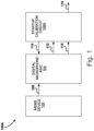
- FIG. 1 is a block diagram of a digital microphone 100A including a MEMS device 102, an ASIC 104 including an open loop VCO-based ADC architecture, and a startup calibration circuit 106A, according to an embodiment.
- MEMS device 102 generates an analog signal at node 108, which is received as an input by ASIC 104.
- ASIC generates digital signals at node 112 and node 114 received by startup calibration circuit 106, and receives a digital signal from startup calibration circuit 106 at node 110.
- Startup calibration circuit 106 provides a digital output signal at output node 116.
- the ASIC 104 is described in further detail below with respect to the block diagram of Figure 2
- the startup calibration circuit 106 is described in further detail below with respect to the block diagram of Figure 3A .
- FIG 2 is a more detailed block diagram of the digital microphone ASIC 104 shown in Figure 1 .
- digital microphone ASIC 104 comprises a VCO-based ADC architecture.
- the ADC architecture comprises has two branches including a first modulator 210 and a second modulator 212. Each modulator comprises a VCO in an embodiment.
- the outputs of first modulator 210 and second modulator 212 are respectively sampled by a first sampler 216 and a second sampler 218.
- the output of the first sampler 216 is coupled to a first inverse Z-transform component 220, and the output of the second sampler 218 is coupled to a second inverse Z-transform component 222.
- the output of the first inverse Z-transform component 220 and a positive input of difference circuit 230 are coupled to node 224.
- the output of the second inverse Z-transform component 222 and a negative input of difference circuit 230 are coupled to node 226.
- the difference of the two inverse Z-transform signals gives the final ADC output at node 114.
- ASIC 104 also includes a number of components that are used in a startup calibration mode, which is described in further detail below.
- ASIC 104 includes a disconnect circuit 202 for disconnecting the ASIC input from node 108 during the startup calibration mode.
- Disconnect circuit 202 receives a control signal on node 110 for selectively engaging or disengaging the disconnect function.
- the output of the disconnect circuit 202 is coupled to a positive input of summer 204 and a negative input of summer 206.
- An output of digital-to-analog converter (DAC) 208 is coupled to another positive input of summer 204 and a positive input of summer 206.
- DAC digital-to-analog converter
- ASIC 104 includes a summer 228 having a first input coupled to node 224 and a second input coupled to node 226, and an output for providing a digital calibration signal at node 114.
- FIG 3A is a more detailed block diagram of the startup calibration circuit 106A shown in Figure 1 .
- Startup calibration circuit 106A includes a control circuit 302 for generating a control signal on node 110, and a calibration calculation block 304.
- calibration calculation block 304 comprises a general purpose processor or a logic circuit for implementing calculation algorithms.
- the calibration calculation block 304 receives the digital calibration signal at node 112, and another control signal from control circuit 302.
- Control circuit 302 and calibration calculation block 304 comprise a calibration signal in an embodiment.
- Startup calibration circuit 106A also includes a signal path including a DC removal circuit 306 coupled to node 114, a multiplication circuit 308 having a first input coupled to the output of the calibration calculation block 304 at node 305 and a second input coupled to the output of DC removal circuit 306.
- the multiplication circuit 308 is configured to perform a desired multiplication function such as "shift and add" multiplication, "bit serial” multiplication, or array multiplication, among other such digital multiplication techniques.
- Startup calibration circuit 106A also includes a digital filter 310 coupled to the output of the multiplication circuit 308, and an optional one-bit digital modulator 312 coupled between the output of digital filter 310 and output node 116.
- the startup calibration circuit 106A can be fabricated on the same integrated circuit as ASIC 104.
- the startup calibration method is implemented for measuring and correcting the sensitivity of the digital microphone during a startup mode of operation, in an embodiment.
- Other digital microphone parameters other than sensitivity, can also be used and are reviewed below.
- the digital microphone sensitivity is measured during startup by sequentially applying two constant values via DAC 208 (DAC code 1 and DAC code 2 stored in register 214). It is important to note that during the sensitivity measurement the input of ASIC 104 is disconnected (or isolated, i.e. no audio signal is added to the input signal). Thus, during startup disconnection of the ASIC 104 input is accomplished using disconnect circuit 202, previously described.
- the sum (using summer 228) of the signals at node 224 and node 226 (“output for calibration") is evaluated (e.g. averaged to get a measurement result with high resolution).
- the sensitivity of the VCO-based ADC in ASIC 104 is calculated and finally the appropriate correction gain is determined.
- the correction gain is then applied to the signal path (using multiplication circuit 308) to adjust the sensitivity to the desired target level, if a deviation due to process or changed clock frequency occurs.
- the "nominal" ADC gain is measured for a "reference or nominal” ADC. That is for a given default operating mode, default room temperature, nominal process and nominal sampling frequency (for example, 3.072 MHz).
- DAC code 1 a first input reference voltage is applied (DAC code 1, as shown in Figure 2 ), and the corresponding digital output in the summing path is obtained (on node 112).
- This digital output at node 112 can be averaged (inside of calibration calculation block 304) for a variable number of sampling clocks, to reduce the effects of noise (such as quantization, common mode noise, or other noise sources).
- a first digital number designated "calib1" is thus obtained.
- a temperature calibration method for example is described below with respect to the embodiments of Figures 4A-7 that cover gain correction for both startup and continuous operation, in contrast to the embodiment of Figure 3A wherein the gain correction is calculated and applied only during a startup mode of operation.
- additional information can also be extracted from the "calib1" and "calib2" digital numbers described above.
- the "calib1" magnitude can be used to identify fast or slow samples and eventually reconfigure the VCO in the VCO-based ADC.
- the "calib1" and “calib2" digital numbers can also be used to avoid an integer ratio between a VCO free running frequency and a sampling frequency that might cause increase noise due to sub-sampling of the VCO by a slower Fclk sampling frequency.
- FIG 3B is a contextual figure showing further details of the calibration calculation block 304 in context with selected other components shown in Figure 3A and Figure 2 .
- Calibration calculation block 304 comprises an averaging filter 314 coupled to node 112, a difference component 316 for calculating the difference of the DAC code 1 and the DAC code 2 measurements coupled to the averaging filter 314, and a normalization component 318 for normalizing the difference with the "kvco_nom" value.
- the normalization component 318 is coupled between the output of normalization component 318 and node 305.
- Calibration calculation block 304 is also coupled to control circuit 302, which in turn is coupled to disconnect circuit 202, and register 214 as previously described.
- FIG. 3C is a flow chart 319 of a startup calibration algorithm according to an embodiment.
- the MEMS signal from MEMS device 102 is disconnected from ASIC 104 at step 320.
- DAC code 1 is applied and the value of "calib1” is calculated at step 322.
- DAC code 2 is applied and the value of "calib2" is calculated at step 324.
- the difference between "calib1" and “calib2” is determined at step 326.
- the difference is normalized with "kvco_nom” at step 328.
- the correction gain for sensitivity compensation is provided at step 330.
- the MEMS signal from MEMS device 102 is reconnected to ASIC 104 at step 332.
- an architecture for a VCO-based ADC has been described that includes a startup calibration mode for maintaining sensitivity stability in a digital microphone, according to an embodiment.
- calibration of any parameters of a digital microphone could also be used during startup.
- the sensitivity stability calibration during startup describe herein, is just one example. Alternative calibration methods are described below.
- the digital microphone sensitivity change due to the change of an external clock could also be calibrated using other methods.
- the "delta” can be determined using an accurate clock frequency detection circuit (CFD, which is a circuit found in many digital microphones).
- CFD clock frequency detection circuit
- the "delta” could also be measured in other ways and used for sensitivity calibration in some embodiments.
- the sensitivity change can also be calibrated with an adaptation algorithm during startup.
- a training sequence is applied via the DAC 208 (described above) and the delta sensitivity is determined by an adaptation algorithm (e.g. gradient approach, sign-sign algorithm, or other such algorithms).
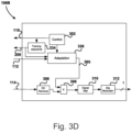
- FIG. 3D is a more detailed block diagram of an alternative startup calibration circuit 106B, suitable for use with the adaptation algorithm embodiment.
- Startup calibration circuit 106B includes several components and nodes that were previously described with respect to startup calibration circuit 106A.
- startup calibration circuit 106B includes a control circuit 302, a DC removal circuit 306, a multiplication circuit 308, a digital filter 310, and a digital modulator 312 were all previously described.
- node 110, node 112, and node 114 were all previously described.
- Startup calibration circuit 106B includes a training sequence register 334 and an adaptation algorithm component 336.
- Training sequence register 334 has an output coupled to node 209, which is the input of DAC 208.
- register 214 of ASIC 104 is omitted.
- the output of training sequence register 334 is also coupled to a first input of the adaptation algorithm component 336.
- a second input of the adaptation component is coupled to node 112.
- the output of the adaptation algorithm component 336 is coupled to node 305.
- Figure 3E is a contextual figure showing further details of an adaptation algorithm block 338 including training sequence register 334 and adaptation algorithm component 336 previously described.
- Adaptation algorithm block 338 is shown in context with selected other components shown in Figure 3D and Figure 2 .
- Training sequence register 334 has an input coupled to node 110.
- An output of control circuit 302 is coupled to an input of adaptation algorithm component 336.
- the output of adaptation algorithm component 336 is coupled to node 305.
- Control circuit 302 is in turn is coupled to disconnect circuit 202 and DAC 208 as previously described.
- Figure 3F is a flow chart 340 of the adaptation algorithm.
- the MEMS signal from MEMS device 102 is disconnected from ASIC 104 at step 342.
- a training sequence is applied to DAC 208 at step 344.
- the training sequence is also provided to the input of the adaptation algorithm component 336 at step 346.
- the correction gain is provided at node 305 for the sensitivity compensation at step 348.
- the MEMS signal from MEMS device 102 can be reconnected to ASIC 104 at step 350.
- the sensitivity change due to ASIC semiconductor process variations could also be calibrated by monitoring the delta in ASIC process fabrication, by monitoring the reference oscillator frequency and/or bandgap/reference currents. To correct the sensitivity due to the deviation from nominal process just the delta is needed, and this could be coded into an internal Look-up-Table, for example.
- a temperature sensor might be used and the corresponding correction applied, based on the delta from default (room temperature).
- a technique for temperature calibration that can be used in either startup mode or during normal operation is described below with respect to Figures 4A-7 .
- sensitivity stability is usually within a certain specified range (e.g. nominal+/-0.5 dB). It is desirable that sensitivity stability meet this specification over process corners, sampling frequency variation, and also temperature variations.
- KVCO depends on process, voltage and temperature. KVCO changing with temperature during normal operation means that sensitivity will also drift without any additional correction method.
- a method and implementation for temperature calibration of a digital microphone is also described, which substantially solves sensitivity drift due to temperature drift in VCO-based digital microphone ADC architectures, especially for the temperature dependency during normal operation. Temperature calibration, however, can also be performed during a startup mode to ensure that even the initial sensitivity of the digital microphone is within specification limits. In general, the gain of the digital microphone is corrected depending on the temperature during operation to keep the sensitivity within a certain specified range. Temperature calibration embodiments also advantageously address preventing audible artefacts due to changing the digital microphone sensitivity during normal operation. An instant gain-change can cause such audible artefacts. Instead, a "ramping" change of the gain from an initial value to a corrected value is implemented to prevent the audible artefacts.
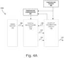
- FIG. 4A is a block diagram of a digital microphone 100B having a temperature calibration circuit including a MEMS device 102, an ASIC 104 including a VCO-based ADC architecture, a startup calibration circuit 106, as well as node 108, node 110, node 112, node 114, and output node 116, all previous described.
- Digital microphone 100B includes a temperature sensor 402 for sensing the current temperature coupled to an input of temperature compensation circuit 404, and to an input of the startup calibration circuit 106, in an embodiment.
- An output of startup calibration circuit 106 is coupled to an input of the temperature compensation circuit 404, in an embodiment.
- An output of temperature compensation circuit 404 is coupled to the ASIC 104, according to embodiments.
- the temperature-based extra gain correction provided by the temperature compensation circuit 404 can be injected into any part of the signal path of digital microphone 100B including the signal path portion in the digital microphone ASIC 104, or in the signal path portion in the startup calibration circuit 106. In the case where ASIC 104 and the startup calibration circuit 106 are combined in a single ASIC, then the extra gain correction provided by temperature compensation circuit 404 can be injected into any part of the signal of the combined single ASIC. While a particular topology for interconnecting the components is shown in Figure 4A , it will be clear to those skilled in the art that various other partitioning and interconnection of these components is possible in other embodiments.
- the temperature compensation circuit 404 is explained in further detail below and includes a ramping circuit for preventing audible artefacts when used during a continuous mode of operation.
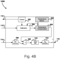
- FIG. 4B is a more detailed block diagram of the startup calibration circuit 106B of Figure 4A including the temperature sensor 402 and the temperature compensation circuit 404.
- Startup calibration circuit 106B also includes control circuit 302, calibration calculation block 304, DC removal circuit 306, multiplication circuit 308, digital filter 310, node 110, node 112, node 114, and output node 116, all previously described.
- the temperature sensor 402 comprises any appropriate integrated circuit temperature sensor.
- the output of temperature sensor which is a voltage proportional to the sensed temperature, is received by both the calibration calculation block 304 and the temperature compensation circuit 404.
- the temperature compensation circuit 404 has an input coupled to an output of the calibration calculation block 304 and an output coupled to an input of multiplication circuit 308.
- startup calibration circuit 106B calculates a correction gain to adjust the sensitivity of the digital microphone 100B to a target level.
- the correction gain is applied to the signal path of digital microphone 100B, if a deviation due to process or changed clock frequency occurs.
- the correction gain is applied to an input of multiplication circuit 308 during a startup mode of operation, in an embodiment.
- the temperature compensation circuit 404 compensates the temperature dependency of the VCO-based architecture by adding a further temperature-dependent correction gain. Further details of temperature compensation circuit 404 are described below.
- the VCO-based ADC architecture of digital microphone 100B supports different operating modes (e.g. low power mode, normal mode, and high performance mode). Each one of these different operating modes requires a different temperature correction. It is important to note that temperature compensation according to embodiments can be performed both in the startup phase and during the continuous mode of operation.
- the temperature compensation circuit makes no differentiation between the low power, normal or high performance mode.
- the temperature compensation in the continuous mode of operation compensate possible sensitivity drift independent of the specific operating mode.
- Figure 5 is a graph 500 of a plurality of stepped gain correction traces realized with look-up-tables (LUTs), corresponding to a plurality of different operating modes.
- the stepped or ramped gain is explained in further detail below with respect to Figure 6 and Figure 7 .
- the x-axis of Figure 5 shows time steps of the correction gain in unit steps, and the y-axis of Figure 5 shows the change in the correction in decibels (dB) for three different operating modes.
- the x-axis reflects the difference between a reference-point (the startup-calibration temperature window) and the actual temperature window.
- the temperature sensor provides the temperature information and a coarse quantized information called a temperature window, which is sufficient for the delta-gain estimation/calculation.
- Trace 506 corresponds to a low power mode
- trace 504 corresponds to a normal mode
- trace 502 corresponds to a high performance mode.
- These three traces (506, 504, and 502) are only examples of how the different operation modes of the digital microphone are addressed according to an embodiment.
- the absolute values of the trace values are dependent on the VCO-ADC design and are adjusted accordingly for a specific implementation.
- the startup calibration circuit 106B stores (for example in a register inside calibration calculation block 304) the temperature value at which the calibration was performed. The correction gain during operation is thus calculated relative to the "startup-calibration" temperature.
- FIG. 6 is a more detailed block diagram of the temperature compensation circuit 404 shown in Figure 4B , including a ramp circuit 618, according to an embodiment.
- Temperature compensation circuit 404 includes a difference circuit 610 having a positive input for receiving the startup calibration temperature at node 602 and a negative input for receiving the actual sensed temperature at node 604.
- the output of difference circuit 610 is coupled to a first input of multiplication circuit 614.
- the output of the difference circuit 610 is the input for the LUT 612 (containing the values of traces 506, 504, 502).
- the output of the LUT 612 is provides a delta gain that is combined with the startup calibration gain (input node 606) in multiplication circuit 614.
- the output of summer 616 reflects the correct gain delta which needs to be applied to the ramp circuit 618.
- the second input of multiplication circuit 614 receives the startup calibration gain at node 606.
- the output of difference circuit 610 is also coupled to a first input of summer 616.
- a second input of summer 616 is coupled to the output of multiplication circuit 614.
- the output of summer 616 is coupled to an input of ramp circuit 618.
- the ramp circuit 618 also receives a mode signal at node 608 indicative of the mode (low power model, normal mode, or high performance mode) of digital microphone 100B.
- the temperature compensation circuit 404 does not immediately apply the "correction gain" when the temperature sensor 402 changes its output value due to sensing a new ambient temperature. To do so would cause an audio artefact as previously described.
- the correction gain is slowly ramped up/down from the current value to a calculated target value as is shown in Figure 5 .
- the ramping logic supports different modes to ensure the same timing behavior of the correction gain (e.g. the three operating modes have corresponding clock frequencies of 768kHz, 1.5MHz, and 3.072MHz, in an embodiment). Other or additional clock frequencies can be supported in other embodiments. For example some digital microphones may have additional operating modes such as an extended clock mode requiring another clock frequency.
- Ramp circuit 618 can be realized with a clock-gating circuit that has very low power consumption, which is described in further detail below with respect to Figure 7 .
- the ramp-timing of ramp circuit 618 can be easily readjusted (using LUTs, registers, or other components) and is also mode dependent (low power mode, normal mode, high performance mode).
- the ramp-timing and the gain step-size ensure are configured so that no audible artefacts are generated.
- the ramp-timing and gain step-size are not signal dependent as is explained in further detail below with respect to Figure 7 .
- the ramp-timing and gain step-size described herein and shown in Figure 5 are only one example of ramping the correction gain. The exact timing and shape of the correction gain ramp, as well as the gain step-size itself, can be changed in other embodiments without generating audible artefacts.
- FIG. 7 is a more detailed block diagram of the ramp circuit 618 shown in Figure 6 , according to an embodiment.
- Ramp circuit 618 includes a pre-scaling block 706 having an input for receiving a gain signal from the output of summer 616 at input node 702.
- Ramp circuit 618 also includes an identity block 708 having an input for receiving a ramp timing signal at node 704 (equivalent to the "mode" signal at node 608 previously described).
- the output of the pre-scaling block 706 is coupled to an input of a first inverse Z-transform block 712 (also known as a clock-gating register).
- the output of first inverse Z-transform block 712 is coupled to a positive input of difference circuit 714.
- the output of difference circuit 714 is coupled to an input of "sign" block 718.
- the function of the sign block 718 is a minus one output for a negative input value, a zero output for a zero input, and a plus one output for a positive input value.
- the output of sign block 718 is coupled to a first positive input of adder 720, and the negative input of difference circuit 714 is coupled to a second positive input of adder 720.
- the output of adder 720 is coupled to an input of multiplexer 725.
- Another input of multiplexer 725 is coupled to an output of a zero bit register 722.
- the output of multiplexer 725 is fed back to the negative input of difference circuit 714 through a second inverse Z-transform block 716.
- the control inputs of the first inverse Z-transform block 712 and the second inverse Z-transform block 716 are coupled to the output of identity block 708.
- a counter 710 is coupled between the output of identity block 708 and a second input of identity block 708.
- the output of multiplexer provides the output of ramp circuit 618 at node 620.
- the output signal coming of identity block 708 is the clock-enable signal (a control signal) which acts as a clock-gating signal. Only on each n-th cycle an update of the registers are performed in response to the main-clock (power saving technique).
- Counter 710 runs on the main-clock rate, and if the identity block 708 reaches its condition (counter output equal input at node 704), then for one cycle the clock-enable signal is triggered and the counter is also reset. This is a simple way to generate an equidistant time-grid.
- difference circuit 714 calculates the difference between a "new gain” and the current state.
- ramp circuit 618 performs a "first glance” on the direction using sign block 718.
- Adder 720 combines the information (gain) of the current state plus or minus one LSB into the direction of the "new" gain state. This is done until the "new" gain state with is reached using second inverse Z-transform block 716.
- a slow integration upwards/downwards from the current gain state to the new gain state is performed by ramp circuit 618, according to an embodiment.
- Zero bit register 722 allows for the possibility of resetting the digital microphone in an embodiment.
- the ramp circuit 618 provides the ramping behavior realized with clock-gating functionality (for power saving reasons).
- a gain-change applied at the input node 702 leads to an up/down ramping depending if the actual gain is smaller/bigger than the new applied one. Since the stepping is done in one LSB steps, the gain-step-size is realized with the pre-scaling block 706.
- the ramp-timing and the gain step-size ensure that no audible artefacts are generated. Furthermore there is no signal dependent logic needed (e.g. zero crossing check).
- the temperature calibration architecture described above with respect to Figures 4 through 7 compensates sensitivity drift due to temperature-dependency of the VCO-based architecture in the digital microphone during operation.
- the compensation is advantageously performed in a manner such that no audible artefacts are generated.
- Figure 8 is a flow chart of a method 800 of operating a digital microphone, according to an embodiment.
- Method 800 comprises modulating an analog input signal to generate a first digital signal at step 802; modulating the analog input signal to generate a second digital signal at step 804; summing the first digital signal and the second digital signal to generate a digital calibration path signal at step 806; and determining a difference between the first digital signal and the second digital signal to generate a digital signal path signal at step 808.
- Method 800 further comprises applying a digital calibration path signal to a calibration path in a startup calibration mode of operation, and applying a digital signal path signal to a signal path in a normal mode of operation.
- Method 800 further comprises calculating a correction gain in the startup calibration mode of operation, and applying the correction gain to the signal path in the normal mode of operation. Method 800 further comprising adjusting the correction gain to correspond to one of a plurality of operating modes. Method 800 further comprises ramping the correction gain from an initial correction gain based on an initial temperature to a current correction gain based on a current temperature.
- a digital microphone comprises a first modulation path having an input for receiving an analog input signal and an output for generating a first digital signal; a second modulation path having an input for receiving the analog input signal and an output for generating a second digital signal; a summing circuit having a first input for receiving the first digital signal, a second input for receiving the second digital signal, and an output for generating a digital calibration path signal; and a difference circuit having a first input for receiving the first digital signal, a second input for receiving the second digital signal, and an output for generating a digital signal path signal.
- Example 2 The digital microphone of Example 1, wherein the output of the summing circuit is energized in a startup calibration mode of operation, and wherein the output of the difference circuit is energized in a normal mode of operation.
- Example 3 The digital microphone of any of the above examples, further comprising a disconnect circuit for isolating the first modulation path and the second modulation path from the analog input signal during the startup calibration mode of operation.
- Example 4 The digital microphone of any of the above examples, further comprising a digital-to-analog converter (DAC) circuit having an input for receiving a control signal and an output coupled to the input of the first modulation path and to the input of the second modulation path.
- DAC digital-to-analog converter
- Example 5 The digital microphone of any of the above examples, wherein the DAC circuit comprises a memory for storing first and second DAC codes; and a DAC for receiving the first and second DAC codes.
- Example 6 The digital microphone of any of the above examples, wherein the first modulation path comprises a first voltage-controlled oscillator (VCO) based analog-to-digital (ADC), and wherein the second modulation path comprises a second VCO based ADC.
- VCO voltage-controlled oscillator
- ADC analog-to-digital
- Example 7 The digital microphone of any of the above examples, further comprising a startup calibration circuit having a first input coupled to the output of the summing circuit, a second input coupled to the output of the difference circuit, and an output for generating a digital signal for generating a digital output signal corresponding to the analog input signal during the normal mode of operation.
- Example 8 The digital microphone of any of the above examples, wherein the startup calibration circuit comprises a calibration path and a signal path, wherein the calibration path is coupled between the first input and an internal node of the signal path, and wherein the signal path is coupled between the second input and the output.
- Example 9 The digital microphone of any of the above examples, wherein the calibration path comprises a calibration calculation block configured for generating a correction gain.
- Example 10 The digital microphone of any of the above examples, wherein the signal path comprises a multiplication circuit having an input coupled to the internal node of the signal path.
- a digital microphone comprises an analog-to-digital converter (ADC); a digital signal path coupled to the ADC; a temperature sensor; and a temperature compensation circuit coupled to the temperature sensor and to a node of the digital signal path, wherein the temperature compensation circuit is configured for providing a correction gain to the digital signal path during a normal mode of operation.
- ADC analog-to-digital converter
- Example 12 The digital microphone of Example 11, wherein the ADC comprises a first modulation path having an input for receiving an analog input signal and an output for generating a first digital signal, and a second modulation path having an input for receiving the analog input signal and an output for generating a second digital signal, and wherein the digital signal path comprises a summing circuit having a first input for receiving the first digital signal, a second input for receiving the second digital signal, and an output for generating a digital calibration path signal, and a difference circuit having a first input for receiving the first digital signal, a second input for receiving the second digital signal, and an output for generating a digital signal path signal.
- the ADC comprises a first modulation path having an input for receiving an analog input signal and an output for generating a first digital signal, and a second modulation path having an input for receiving the analog input signal and an output for generating a second digital signal
- the digital signal path comprises a summing circuit having a first input for receiving the first digital signal, a second input for receiving the second digital
- Example 13 The digital microphone of any of the above examples, wherein the digital signal path further comprises a startup calibration circuit.
- Example 14 The digital microphone of any of the above examples, wherein the temperature compensation circuit comprises a lookup table for changing the correction gain to correspond to one of a plurality of operating modes.
- Example 15 The digital microphone of any of the above examples, wherein the temperature compensation circuit comprises a ramping circuit for generating a series of stepped correction gain values.
- Example 16 A method of operating a digital microphone, the method comprising modulating an analog input signal to generate a first digital signal; modulating the analog input signal to generate a second digital signal; summing the first digital signal and the second digital signal to generate a digital calibration path signal; and determining a difference between the first digital signal and the second digital signal to generate a digital signal path signal.
- Example 17 The method of Example 16, wherein the digital calibration path signal is applied to a calibration path in a startup calibration mode of operation, and wherein the digital signal path signal is applied to a signal path in a normal mode of operation.
- Example 18 The method of any of the above examples, further comprising calculating a correction gain in the startup calibration mode of operation, and applying the correction gain to the signal path in the normal mode of operation.
- Example 19 The method of any of the above examples, further comprising adjusting the correction gain to correspond to one of a plurality of operating modes.
- Example 20 The method of any of the above examples, further comprises ramping the correction gain from an initial correction gain based on an initial temperature to a current correction gain based on a current temperature.
Landscapes
- Engineering & Computer Science (AREA)
- Theoretical Computer Science (AREA)
- Physics & Mathematics (AREA)
- Acoustics & Sound (AREA)
- Signal Processing (AREA)
- Health & Medical Sciences (AREA)
- General Health & Medical Sciences (AREA)
- Otolaryngology (AREA)
- Amplifiers (AREA)
Abstract
A digital microphone includes a first modulation path having an input for receiving an analog input signal and an output for generating a first digital signal; a second modulation path having an input for receiving the analog input signal and an output for generating a second digital signal; a summing circuit having a first input for receiving the first digital signal, a second input for receiving the second digital signal, and an output for generating a digital calibration path signal; and a difference circuit having a first input for receiving the first digital signal, a second input for receiving the second digital signal, and an output for generating a digital signal path signal.
Description
- The present invention relates generally to startup calibration and digital temperature compensation for an open-loop voltage-controlled oscillator (VCO)-based analog-to-digital converter (ADC) architecture and, in particular embodiments, to a corresponding method.
- Digital microphones are known in the art. Typically, digital microphones include an application-specific integrated circuit (ASIC) that includes at least one ADC for converting an analog input signal from a microelectromechanical system (MEMS) device into a digital output signal representative of sound waves sensing by the MEMS device. In many existing digital microphones, closed-loop sigma-delta based ADC architectures are used. These ADC architectures generally have sensitivities that are not dependent on sampling frequency and process corners. In some newer digital microphones, open loop VCO-based ADC architectures are used. These open loop VCO-based ADC architectures have several notable advantages such as low power, low integrated circuit area, increased performance (for example increased signal-to-noise ratio), low group delay, and improved shock recovery. However, in some of the newer microphones, these ADC architectures can have sensitivities that are dependent upon sampling frequency, process corners, and temperature.
- According to an embodiment, a digital microphone comprises a first modulation path having an input for receiving an analog input signal and an output for generating a first digital signal; a second modulation path having an input for receiving the analog input signal and an output for generating a second digital signal; a summing circuit having a first input for receiving the first digital signal, a second input for receiving the second digital signal, and an output for generating a digital calibration path signal; and a difference circuit having a first input for receiving the first digital signal, a second input for receiving the second digital signal, and an output for generating a digital signal path signal.
- According to an embodiment, a digital microphone comprises an analog-to-digital converter (ADC); a digital signal path coupled to the ADC; a temperature sensor; and a temperature compensation circuit coupled to the temperature sensor and to a node of the digital signal path, wherein the temperature compensation circuit is configured for providing a correction gain to the digital signal path during a normal mode of operation.
- According to an embodiment, a method of operating a digital microphone, the method comprising modulating an analog input signal to generate a first digital signal; modulating the analog input signal to generate a second digital signal; summing the first digital signal and the second digital signal to generate a digital calibration path signal; and determining a difference between the first digital signal and the second digital signal to generate a digital signal path signal.
- For a more complete understanding of the present invention, and the advantages thereof, reference is now made to the following descriptions taken in conjunction with the accompanying drawings, in which:
-
Figure 1 is a block diagram of a digital microphone including a MEMS device, an ASIC including a VCO-based ADC architecture, and a startup calibration circuit, according to an embodiment; -
Figure 2 is a more detailed block diagram of the ASIC shown inFigure 1 ; -
Figure 3A is a more detailed block diagram of the startup calibration circuit shown inFigure 1 ; -
Figure 3B is a contextual figure showing further details of the calibration calculation block in context with selected other components shown inFigure 3A andFigure 2 ; -
Figure 3C is a flow chart of a startup calibration algorithm according to an embodiment; -
Figure 3D is a more detailed block diagram of an alternative startup calibration circuit according to an embodiment; -
Figure 3E is a contextual figure showing further details of an adaptation algorithm block according to an embodiment; -
Figure 3F is a flow chart of an adaptation algorithm according to an embodiment; -
Figure 4A is a block diagram of a digital microphone including a MEMS device, an ASIC including a VCO-based ADC architecture, a startup calibration circuit, and a temperature compensation circuit coupled either to the ASIC or to the startup calibration circuit, according to embodiments; -
Figure 4B is a more detailed block diagram of the startup calibration circuit ofFigure 4A including the temperature compensation circuit; -
Figure 5 is a graph of a plurality of stepped gain correction traces realized with look-up-tables (LUTs), corresponding to a plurality of different operating modes; -
Figure 6 is a more detailed block diagram of the temperature compensation circuit shown inFigure 4B , including a ramp circuit, according to an embodiment; -
Figure 7 is a more detailed block diagram of the ramp circuit shown inFigure 6 , according to an embodiment; and -
Figure 8 is a flow chart of a method of operating a digital microphone, according to an embodiment. - The making and using of the presently preferred embodiments are discussed in detail below. It should be appreciated, however, that the present invention provides many applicable inventive concepts that can be embodied in a wide variety of specific contexts. The specific embodiments discussed are merely illustrative of specific ways to make and use the invention, and do not limit the scope of the invention.
- In the following detailed description, reference is made to the accompanying drawings, which form a part hereof and in which are shown by way of illustrations specific embodiments in which the invention may be practiced. It is to be understood that other embodiments may be utilized and structural or logical changes may be made without departing from the scope of the present invention. For example, features illustrated or described for one embodiment can be used on or in conjunction with other embodiments to yield yet a further embodiment. It is intended that the present invention includes such modifications and variations. The examples are described using specific language, which should not be construed as limiting the scope of the appending claims. The drawings are not scaled and are for illustrative purposes only. For clarity, the same or similar elements have been designated by corresponding references in the different drawings if not stated otherwise.
- In digital microphones sensitivity is designed to stay within a certain specified range (e.g. nominal+/-0.5 dB). This specification is sometimes known as "sensitivity stability." Sensitivity stability must be fulfilled over process variations, sampling frequency variation, and the operating temperature range. The open-loop VCO-based ADC architecture, described herein, generally has the property that sensitivity depends on sampling frequency and process variations, as well as operating temperature range. The gain of an open-loop VCO-based ADC is given by the following equation:

-
Figure 1 is a block diagram of adigital microphone 100A including aMEMS device 102, an ASIC 104 including an open loop VCO-based ADC architecture, and astartup calibration circuit 106A, according to an embodiment.MEMS device 102 generates an analog signal atnode 108, which is received as an input by ASIC 104. ASIC generates digital signals atnode 112 andnode 114 received bystartup calibration circuit 106, and receives a digital signal fromstartup calibration circuit 106 atnode 110.Startup calibration circuit 106 provides a digital output signal atoutput node 116. TheASIC 104 is described in further detail below with respect to the block diagram ofFigure 2 , and thestartup calibration circuit 106 is described in further detail below with respect to the block diagram ofFigure 3A . -
Figure 2 is a more detailed block diagram of the digital microphone ASIC 104 shown inFigure 1 . In particular, digital microphone ASIC 104 comprises a VCO-based ADC architecture. The ADC architecture comprises has two branches including afirst modulator 210 and asecond modulator 212. Each modulator comprises a VCO in an embodiment. The outputs offirst modulator 210 andsecond modulator 212 are respectively sampled by afirst sampler 216 and asecond sampler 218. The output of thefirst sampler 216 is coupled to a first inverse Z-transform component 220, and the output of thesecond sampler 218 is coupled to a second inverse Z-transform component 222. The output of the first inverse Z-transform component 220 and a positive input ofdifference circuit 230 are coupled tonode 224. The output of the second inverse Z-transform component 222 and a negative input ofdifference circuit 230 are coupled tonode 226. The difference of the two inverse Z-transform signals gives the final ADC output atnode 114. - ASIC 104 also includes a number of components that are used in a startup calibration mode, which is described in further detail below. ASIC 104 includes a
disconnect circuit 202 for disconnecting the ASIC input fromnode 108 during the startup calibration mode.Disconnect circuit 202 receives a control signal onnode 110 for selectively engaging or disengaging the disconnect function. The output of thedisconnect circuit 202 is coupled to a positive input ofsummer 204 and a negative input ofsummer 206. An output of digital-to-analog converter (DAC) 208 is coupled to another positive input ofsummer 204 and a positive input ofsummer 206. An output atnode 209 of register 214 (including first and second DAC codes) is coupled to an input ofDAC 208, and also receives a control signal onnode 110 for toggling between the first and second DAC codes during the startup calibration mode. In addition,ASIC 104 includes asummer 228 having a first input coupled tonode 224 and a second input coupled tonode 226, and an output for providing a digital calibration signal atnode 114. -
Figure 3A is a more detailed block diagram of thestartup calibration circuit 106A shown inFigure 1 .Startup calibration circuit 106A includes acontrol circuit 302 for generating a control signal onnode 110, and acalibration calculation block 304. In an embodiment,calibration calculation block 304 comprises a general purpose processor or a logic circuit for implementing calculation algorithms. Thecalibration calculation block 304 receives the digital calibration signal atnode 112, and another control signal fromcontrol circuit 302.Control circuit 302 andcalibration calculation block 304 comprise a calibration signal in an embodiment.Startup calibration circuit 106A also includes a signal path including aDC removal circuit 306 coupled tonode 114, amultiplication circuit 308 having a first input coupled to the output of thecalibration calculation block 304 atnode 305 and a second input coupled to the output ofDC removal circuit 306. Themultiplication circuit 308 is configured to perform a desired multiplication function such as "shift and add" multiplication, "bit serial" multiplication, or array multiplication, among other such digital multiplication techniques.Startup calibration circuit 106A also includes adigital filter 310 coupled to the output of themultiplication circuit 308, and an optional one-bitdigital modulator 312 coupled between the output ofdigital filter 310 andoutput node 116. In some embodiments, thestartup calibration circuit 106A can be fabricated on the same integrated circuit asASIC 104. - The startup calibration method is implemented for measuring and correcting the sensitivity of the digital microphone during a startup mode of operation, in an embodiment. Other digital microphone parameters, other than sensitivity, can also be used and are reviewed below. In the sensitivity startup calibration method, according to an embodiment, the digital microphone sensitivity is measured during startup by sequentially applying two constant values via DAC 208 (
DAC code 1 andDAC code 2 stored in register 214). It is important to note that during the sensitivity measurement the input ofASIC 104 is disconnected (or isolated, i.e. no audio signal is added to the input signal). Thus, during startup disconnection of theASIC 104 input is accomplished usingdisconnect circuit 202, previously described. For the measurement of the sensitivity of the digital microphone the sum (using summer 228) of the signals atnode 224 and node 226 ("output for calibration") is evaluated (e.g. averaged to get a measurement result with high resolution). Using the two measurement results (one from the first DAC code, and one from the second DAC code) the sensitivity of the VCO-based ADC inASIC 104 is calculated and finally the appropriate correction gain is determined. The correction gain is then applied to the signal path (using multiplication circuit 308) to adjust the sensitivity to the desired target level, if a deviation due to process or changed clock frequency occurs. - Initially, the "nominal" ADC gain is measured for a "reference or nominal" ADC. That is for a given default operating mode, default room temperature, nominal process and nominal sampling frequency (for example, 3.072 MHz). For a "nominal" ADC in "nominal" conditions a first input reference voltage is applied (
DAC code 1, as shown inFigure 2 ), and the corresponding digital output in the summing path is obtained (on node 112). This digital output atnode 112 can be averaged (inside of calibration calculation block 304) for a variable number of sampling clocks, to reduce the effects of noise (such as quantization, common mode noise, or other noise sources). A first digital number designated "calib1" is thus obtained. The same procedure is repeated for a second reference voltage, provided by the same reference DAC (DAC code 2, shown inFigure 2 ). A second digital output "calib2" is thus obtained. The difference between these two digital numbers "calib2" - "calib1" is therefore a direct measure of the overall gain (sensitivity) of the VCO-based ADC inASIC 104. The digital number "kvco_nom" = "calib2" - "calib1" for the "nominal" ADC in "nominal" conditions can be stored in non-volatile memory inside of ASIC 104 (for example inside a register in the calibration calculation block 304). In an embodiment, "kvco_nom" is fused with an individually determined value for every microphone device. In another embodiment, multiple microphone devices are fused with the same "kvco_nom" value (for example all microphone devices on a single wafer.) - The startup calibration method can be used to correct for higher or lower than normal sensitivities. For example, for a given sample, upon startup it is determined that the sampling clock has increased by 10% over the nominal value. The startup algorithm then compute a new "kvco" = "calib2-calib1" which is 10% smaller. The digital algorithm then applies a digital gain of 1.1 (10% higher than 1.00) to correct for this reduced gain/sensitivity. In one implementation, a LUT table is used to efficiently implement this gain. In other embodiments, process, voltage, and initial temperature can also be corrected. A temperature calibration method, for example is described below with respect to the embodiments of
Figures 4A-7 that cover gain correction for both startup and continuous operation, in contrast to the embodiment ofFigure 3A wherein the gain correction is calculated and applied only during a startup mode of operation. - In some embodiments additional information can also be extracted from the "calib1" and "calib2" digital numbers described above. For example, the "calib1" magnitude can be used to identify fast or slow samples and eventually reconfigure the VCO in the VCO-based ADC. For example, the number of programmable gate "fingers" in inverters in the VCO in order to increase overall ASIC yield. The "calib1" and "calib2" digital numbers can also be used to avoid an integer ratio between a VCO free running frequency and a sampling frequency that might cause increase noise due to sub-sampling of the VCO by a slower Fclk sampling frequency.
-
Figure 3B is a contextual figure showing further details of thecalibration calculation block 304 in context with selected other components shown inFigure 3A andFigure 2 .Calibration calculation block 304 comprises an averagingfilter 314 coupled tonode 112, adifference component 316 for calculating the difference of theDAC code 1 and theDAC code 2 measurements coupled to the averagingfilter 314, and anormalization component 318 for normalizing the difference with the "kvco_nom" value. Thenormalization component 318 is coupled between the output ofnormalization component 318 andnode 305.Calibration calculation block 304 is also coupled to controlcircuit 302, which in turn is coupled to disconnectcircuit 202, and register 214 as previously described. -
Figure 3C is aflow chart 319 of a startup calibration algorithm according to an embodiment. The MEMS signal fromMEMS device 102 is disconnected fromASIC 104 atstep 320.DAC code 1 is applied and the value of "calib1" is calculated atstep 322.DAC code 2 is applied and the value of "calib2" is calculated atstep 324. The difference between "calib1" and "calib2" is determined at step 326. The difference is normalized with "kvco_nom" atstep 328. The correction gain for sensitivity compensation is provided atstep 330. The MEMS signal fromMEMS device 102 is reconnected toASIC 104 atstep 332. - In summary, an architecture for a VCO-based ADC has been described that includes a startup calibration mode for maintaining sensitivity stability in a digital microphone, according to an embodiment. However, in other embodiments calibration of any parameters of a digital microphone could also be used during startup. The sensitivity stability calibration during startup describe herein, is just one example. Alternative calibration methods are described below.
- The digital microphone sensitivity change due to the change of an external clock (or deviation from a nominal clock) could also be calibrated using other methods. To correct the sensitivity due to a clock change (or deviation from nominal clock) only the change ("delta") of the clock is required. The "delta" can be determined using an accurate clock frequency detection circuit (CFD, which is a circuit found in many digital microphones). The "delta" could also be measured in other ways and used for sensitivity calibration in some embodiments.
- The sensitivity change can also be calibrated with an adaptation algorithm during startup. In this case a training sequence is applied via the DAC 208 (described above) and the delta sensitivity is determined by an adaptation algorithm (e.g. gradient approach, sign-sign algorithm, or other such algorithms).
-
Figure 3D is a more detailed block diagram of an alternativestartup calibration circuit 106B, suitable for use with the adaptation algorithm embodiment.Startup calibration circuit 106B includes several components and nodes that were previously described with respect tostartup calibration circuit 106A. For example,startup calibration circuit 106B includes acontrol circuit 302, aDC removal circuit 306, amultiplication circuit 308, adigital filter 310, and adigital modulator 312 were all previously described. Similarly,node 110,node 112, andnode 114 were all previously described.Startup calibration circuit 106B includes a training sequence register 334 and anadaptation algorithm component 336. Training sequence register 334 has an output coupled tonode 209, which is the input ofDAC 208. In the adaptation algorithm embodiment, register 214 ofASIC 104 is omitted. The output of training sequence register 334 is also coupled to a first input of theadaptation algorithm component 336. A second input of the adaptation component is coupled tonode 112. The output of theadaptation algorithm component 336 is coupled tonode 305. -
Figure 3E is a contextual figure showing further details of anadaptation algorithm block 338 including training sequence register 334 andadaptation algorithm component 336 previously described.Adaptation algorithm block 338 is shown in context with selected other components shown inFigure 3D andFigure 2 . Training sequence register 334 has an input coupled tonode 110. An output ofcontrol circuit 302 is coupled to an input ofadaptation algorithm component 336. The output ofadaptation algorithm component 336 is coupled tonode 305.Control circuit 302 is in turn is coupled to disconnectcircuit 202 andDAC 208 as previously described. -
Figure 3F is aflow chart 340 of the adaptation algorithm. In operation, the MEMS signal fromMEMS device 102 is disconnected fromASIC 104 atstep 342. A training sequence is applied toDAC 208 atstep 344. The training sequence is also provided to the input of theadaptation algorithm component 336 at step 346. After the adaptation algorithm has settled to a final value, the correction gain is provided atnode 305 for the sensitivity compensation atstep 348. After the correction gain is provided, the MEMS signal fromMEMS device 102 can be reconnected toASIC 104 atstep 350. - The sensitivity change due to ASIC semiconductor process variations could also be calibrated by monitoring the delta in ASIC process fabrication, by monitoring the reference oscillator frequency and/or bandgap/reference currents. To correct the sensitivity due to the deviation from nominal process just the delta is needed, and this could be coded into an internal Look-up-Table, for example.
- Similarly, for the initial temperature dependence, a temperature sensor might be used and the corresponding correction applied, based on the delta from default (room temperature). A technique for temperature calibration that can be used in either startup mode or during normal operation is described below with respect to
Figures 4A-7 . - In digital microphones, as previously described, sensitivity stability is usually within a certain specified range (e.g. nominal+/-0.5 dB). It is desirable that sensitivity stability meet this specification over process corners, sampling frequency variation, and also temperature variations. For VCO-based ADCs used in digital microphones, as previously described, KVCO depends on process, voltage and temperature. KVCO changing with temperature during normal operation means that sensitivity will also drift without any additional correction method.
- According to embodiments a method and implementation for temperature calibration of a digital microphone is also described, which substantially solves sensitivity drift due to temperature drift in VCO-based digital microphone ADC architectures, especially for the temperature dependency during normal operation. Temperature calibration, however, can also be performed during a startup mode to ensure that even the initial sensitivity of the digital microphone is within specification limits. In general, the gain of the digital microphone is corrected depending on the temperature during operation to keep the sensitivity within a certain specified range. Temperature calibration embodiments also advantageously address preventing audible artefacts due to changing the digital microphone sensitivity during normal operation. An instant gain-change can cause such audible artefacts. Instead, a "ramping" change of the gain from an initial value to a corrected value is implemented to prevent the audible artefacts.
-
Figure 4A is a block diagram of a digital microphone 100B having a temperature calibration circuit including aMEMS device 102, anASIC 104 including a VCO-based ADC architecture, astartup calibration circuit 106, as well asnode 108,node 110,node 112,node 114, andoutput node 116, all previous described. Digital microphone 100B includes atemperature sensor 402 for sensing the current temperature coupled to an input oftemperature compensation circuit 404, and to an input of thestartup calibration circuit 106, in an embodiment. An output ofstartup calibration circuit 106 is coupled to an input of thetemperature compensation circuit 404, in an embodiment. An output oftemperature compensation circuit 404 is coupled to theASIC 104, according to embodiments. In pertinent part, the temperature-based extra gain correction provided by thetemperature compensation circuit 404 can be injected into any part of the signal path of digital microphone 100B including the signal path portion in thedigital microphone ASIC 104, or in the signal path portion in thestartup calibration circuit 106. In the case whereASIC 104 and thestartup calibration circuit 106 are combined in a single ASIC, then the extra gain correction provided bytemperature compensation circuit 404 can be injected into any part of the signal of the combined single ASIC. While a particular topology for interconnecting the components is shown inFigure 4A , it will be clear to those skilled in the art that various other partitioning and interconnection of these components is possible in other embodiments. Thetemperature compensation circuit 404 is explained in further detail below and includes a ramping circuit for preventing audible artefacts when used during a continuous mode of operation. -
Figure 4B is a more detailed block diagram of thestartup calibration circuit 106B ofFigure 4A including thetemperature sensor 402 and thetemperature compensation circuit 404.Startup calibration circuit 106B also includescontrol circuit 302,calibration calculation block 304,DC removal circuit 306,multiplication circuit 308,digital filter 310,node 110,node 112,node 114, andoutput node 116, all previously described. Thetemperature sensor 402 comprises any appropriate integrated circuit temperature sensor. The output of temperature sensor, which is a voltage proportional to the sensed temperature, is received by both thecalibration calculation block 304 and thetemperature compensation circuit 404. Thetemperature compensation circuit 404 has an input coupled to an output of thecalibration calculation block 304 and an output coupled to an input ofmultiplication circuit 308. - In operation,
startup calibration circuit 106B calculates a correction gain to adjust the sensitivity of the digital microphone 100B to a target level. The correction gain is applied to the signal path of digital microphone 100B, if a deviation due to process or changed clock frequency occurs. In particular, the correction gain is applied to an input ofmultiplication circuit 308 during a startup mode of operation, in an embodiment. - During a continuous operation of digital microphone 100B, the
temperature compensation circuit 404 compensates the temperature dependency of the VCO-based architecture by adding a further temperature-dependent correction gain. Further details oftemperature compensation circuit 404 are described below. The VCO-based ADC architecture of digital microphone 100B supports different operating modes (e.g. low power mode, normal mode, and high performance mode). Each one of these different operating modes requires a different temperature correction. It is important to note that temperature compensation according to embodiments can be performed both in the startup phase and during the continuous mode of operation. The temperature compensation circuit makes no differentiation between the low power, normal or high performance mode. The temperature compensation in the continuous mode of operation compensate possible sensitivity drift independent of the specific operating mode. -
Figure 5 is agraph 500 of a plurality of stepped gain correction traces realized with look-up-tables (LUTs), corresponding to a plurality of different operating modes. The stepped or ramped gain is explained in further detail below with respect toFigure 6 andFigure 7 . The x-axis ofFigure 5 shows time steps of the correction gain in unit steps, and the y-axis ofFigure 5 shows the change in the correction in decibels (dB) for three different operating modes. The x-axis reflects the difference between a reference-point (the startup-calibration temperature window) and the actual temperature window. The temperature sensor provides the temperature information and a coarse quantized information called a temperature window, which is sufficient for the delta-gain estimation/calculation.Trace 506 corresponds to a low power mode,trace 504 corresponds to a normal mode, and trace 502 corresponds to a high performance mode. These three traces (506, 504, and 502) are only examples of how the different operation modes of the digital microphone are addressed according to an embodiment. The absolute values of the trace values are dependent on the VCO-ADC design and are adjusted accordingly for a specific implementation. - To calculate the correct gain during the normal mode of operation, the
startup calibration circuit 106B stores (for example in a register inside calibration calculation block 304) the temperature value at which the calibration was performed. The correction gain during operation is thus calculated relative to the "startup-calibration" temperature. -
Figure 6 is a more detailed block diagram of thetemperature compensation circuit 404 shown inFigure 4B , including aramp circuit 618, according to an embodiment.Temperature compensation circuit 404 includes adifference circuit 610 having a positive input for receiving the startup calibration temperature atnode 602 and a negative input for receiving the actual sensed temperature atnode 604. The output ofdifference circuit 610 is coupled to a first input ofmultiplication circuit 614. The output of thedifference circuit 610 is the input for the LUT 612 (containing the values oftraces LUT 612 is provides a delta gain that is combined with the startup calibration gain (input node 606) inmultiplication circuit 614. - The output of
summer 616 reflects the correct gain delta which needs to be applied to theramp circuit 618. The second input ofmultiplication circuit 614 receives the startup calibration gain atnode 606. The output ofdifference circuit 610 is also coupled to a first input ofsummer 616. A second input ofsummer 616 is coupled to the output ofmultiplication circuit 614. The output ofsummer 616 is coupled to an input oframp circuit 618. Theramp circuit 618 also receives a mode signal atnode 608 indicative of the mode (low power model, normal mode, or high performance mode) of digital microphone 100B. - In operation, the
temperature compensation circuit 404 does not immediately apply the "correction gain" when thetemperature sensor 402 changes its output value due to sensing a new ambient temperature. To do so would cause an audio artefact as previously described. Instead of an instant gain-step, the correction gain is slowly ramped up/down from the current value to a calculated target value as is shown inFigure 5 . The ramping logic supports different modes to ensure the same timing behavior of the correction gain (e.g. the three operating modes have corresponding clock frequencies of 768kHz, 1.5MHz, and 3.072MHz, in an embodiment). Other or additional clock frequencies can be supported in other embodiments. For example some digital microphones may have additional operating modes such as an extended clock mode requiring another clock frequency. -
Ramp circuit 618 can be realized with a clock-gating circuit that has very low power consumption, which is described in further detail below with respect toFigure 7 . The ramp-timing oframp circuit 618 can be easily readjusted (using LUTs, registers, or other components) and is also mode dependent (low power mode, normal mode, high performance mode). The ramp-timing and the gain step-size ensure are configured so that no audible artefacts are generated. In an embodiment, the ramp-timing and gain step-size are not signal dependent as is explained in further detail below with respect toFigure 7 . The ramp-timing and gain step-size described herein and shown inFigure 5 are only one example of ramping the correction gain. The exact timing and shape of the correction gain ramp, as well as the gain step-size itself, can be changed in other embodiments without generating audible artefacts. -
Figure 7 is a more detailed block diagram of theramp circuit 618 shown inFigure 6 , according to an embodiment.Ramp circuit 618 includes apre-scaling block 706 having an input for receiving a gain signal from the output ofsummer 616 atinput node 702.Ramp circuit 618 also includes anidentity block 708 having an input for receiving a ramp timing signal at node 704 (equivalent to the "mode" signal atnode 608 previously described). The output of thepre-scaling block 706 is coupled to an input of a first inverse Z-transform block 712 (also known as a clock-gating register). The output of first inverse Z-transform block 712 is coupled to a positive input ofdifference circuit 714. The output ofdifference circuit 714 is coupled to an input of "sign"block 718. The function of thesign block 718 is a minus one output for a negative input value, a zero output for a zero input, and a plus one output for a positive input value. The output ofsign block 718 is coupled to a first positive input ofadder 720, and the negative input ofdifference circuit 714 is coupled to a second positive input ofadder 720. The output ofadder 720 is coupled to an input ofmultiplexer 725. Another input ofmultiplexer 725 is coupled to an output of a zerobit register 722. The output ofmultiplexer 725 is fed back to the negative input ofdifference circuit 714 through a second inverse Z-transform block 716. The control inputs of the first inverse Z-transform block 712 and the second inverse Z-transform block 716 are coupled to the output ofidentity block 708. Acounter 710 is coupled between the output ofidentity block 708 and a second input ofidentity block 708. The output of multiplexer provides the output oframp circuit 618 atnode 620. - The output signal coming of
identity block 708 is the clock-enable signal (a control signal) which acts as a clock-gating signal. Only on each n-th cycle an update of the registers are performed in response to the main-clock (power saving technique). Counter 710 runs on the main-clock rate, and if theidentity block 708 reaches its condition (counter output equal input at node 704), then for one cycle the clock-enable signal is triggered and the counter is also reset. This is a simple way to generate an equidistant time-grid. - In operation,
difference circuit 714 calculates the difference between a "new gain" and the current state. To perform the ramping,ramp circuit 618 performs a "first glance" on the direction usingsign block 718.Adder 720 combines the information (gain) of the current state plus or minus one LSB into the direction of the "new" gain state. This is done until the "new" gain state with is reached using second inverse Z-transform block 716. In summary, a slow integration upwards/downwards from the current gain state to the new gain state is performed byramp circuit 618, according to an embodiment. Zero bit register 722 allows for the possibility of resetting the digital microphone in an embodiment. - In operation the
ramp circuit 618 provides the ramping behavior realized with clock-gating functionality (for power saving reasons). A gain-change applied at theinput node 702 leads to an up/down ramping depending if the actual gain is smaller/bigger than the new applied one. Since the stepping is done in one LSB steps, the gain-step-size is realized with thepre-scaling block 706. The ramp-timing and the gain step-size ensure that no audible artefacts are generated. Furthermore there is no signal dependent logic needed (e.g. zero crossing check). - In summary, the temperature calibration architecture described above with respect to
Figures 4 through 7 compensates sensitivity drift due to temperature-dependency of the VCO-based architecture in the digital microphone during operation. The compensation is advantageously performed in a manner such that no audible artefacts are generated. -
Figure 8 is a flow chart of amethod 800 of operating a digital microphone, according to an embodiment.Method 800 comprises modulating an analog input signal to generate a first digital signal atstep 802; modulating the analog input signal to generate a second digital signal atstep 804; summing the first digital signal and the second digital signal to generate a digital calibration path signal atstep 806; and determining a difference between the first digital signal and the second digital signal to generate a digital signal path signal atstep 808.Method 800 further comprises applying a digital calibration path signal to a calibration path in a startup calibration mode of operation, and applying a digital signal path signal to a signal path in a normal mode of operation.Method 800 further comprises calculating a correction gain in the startup calibration mode of operation, and applying the correction gain to the signal path in the normal mode of operation.Method 800 further comprising adjusting the correction gain to correspond to one of a plurality of operating modes.Method 800 further comprises ramping the correction gain from an initial correction gain based on an initial temperature to a current correction gain based on a current temperature. - Example embodiments of the present invention are summarized here. Other embodiments can also be understood from the entirety of the specification and the claims filed herein.
- Example 1. A digital microphone comprises a first modulation path having an input for receiving an analog input signal and an output for generating a first digital signal; a second modulation path having an input for receiving the analog input signal and an output for generating a second digital signal; a summing circuit having a first input for receiving the first digital signal, a second input for receiving the second digital signal, and an output for generating a digital calibration path signal; and a difference circuit having a first input for receiving the first digital signal, a second input for receiving the second digital signal, and an output for generating a digital signal path signal.
- Example 2. The digital microphone of Example 1, wherein the output of the summing circuit is energized in a startup calibration mode of operation, and wherein the output of the difference circuit is energized in a normal mode of operation.
- Example 3. The digital microphone of any of the above examples, further comprising a disconnect circuit for isolating the first modulation path and the second modulation path from the analog input signal during the startup calibration mode of operation.
- Example 4. The digital microphone of any of the above examples, further comprising a digital-to-analog converter (DAC) circuit having an input for receiving a control signal and an output coupled to the input of the first modulation path and to the input of the second modulation path.
- Example 5. The digital microphone of any of the above examples, wherein the DAC circuit comprises a memory for storing first and second DAC codes; and a DAC for receiving the first and second DAC codes.
- Example 6. The digital microphone of any of the above examples, wherein the first modulation path comprises a first voltage-controlled oscillator (VCO) based analog-to-digital (ADC), and wherein the second modulation path comprises a second VCO based ADC.
- Example 7. The digital microphone of any of the above examples, further comprising a startup calibration circuit having a first input coupled to the output of the summing circuit, a second input coupled to the output of the difference circuit, and an output for generating a digital signal for generating a digital output signal corresponding to the analog input signal during the normal mode of operation.
- Example 8. The digital microphone of any of the above examples, wherein the startup calibration circuit comprises a calibration path and a signal path, wherein the calibration path is coupled between the first input and an internal node of the signal path, and wherein the signal path is coupled between the second input and the output.
- Example 9. The digital microphone of any of the above examples, wherein the calibration path comprises a calibration calculation block configured for generating a correction gain.
- Example 10. The digital microphone of any of the above examples, wherein the signal path comprises a multiplication circuit having an input coupled to the internal node of the signal path.
- Example 11. A digital microphone comprises an analog-to-digital converter (ADC); a digital signal path coupled to the ADC; a temperature sensor; and a temperature compensation circuit coupled to the temperature sensor and to a node of the digital signal path, wherein the temperature compensation circuit is configured for providing a correction gain to the digital signal path during a normal mode of operation.
- Example 12. The digital microphone of Example 11, wherein the ADC comprises a first modulation path having an input for receiving an analog input signal and an output for generating a first digital signal, and a second modulation path having an input for receiving the analog input signal and an output for generating a second digital signal, and wherein the digital signal path comprises a summing circuit having a first input for receiving the first digital signal, a second input for receiving the second digital signal, and an output for generating a digital calibration path signal, and a difference circuit having a first input for receiving the first digital signal, a second input for receiving the second digital signal, and an output for generating a digital signal path signal.
- Example 13. The digital microphone of any of the above examples, wherein the digital signal path further comprises a startup calibration circuit.
- Example 14. The digital microphone of any of the above examples, wherein the temperature compensation circuit comprises a lookup table for changing the correction gain to correspond to one of a plurality of operating modes.
- Example 15. The digital microphone of any of the above examples, wherein the temperature compensation circuit comprises a ramping circuit for generating a series of stepped correction gain values.
- Example 16. A method of operating a digital microphone, the method comprising modulating an analog input signal to generate a first digital signal; modulating the analog input signal to generate a second digital signal; summing the first digital signal and the second digital signal to generate a digital calibration path signal; and determining a difference between the first digital signal and the second digital signal to generate a digital signal path signal.
- Example 17. The method of Example 16, wherein the digital calibration path signal is applied to a calibration path in a startup calibration mode of operation, and wherein the digital signal path signal is applied to a signal path in a normal mode of operation.
- Example 18. The method of any of the above examples, further comprising calculating a correction gain in the startup calibration mode of operation, and applying the correction gain to the signal path in the normal mode of operation.
- Example 19. The method of any of the above examples, further comprising adjusting the correction gain to correspond to one of a plurality of operating modes.
- Example 20. The method of any of the above examples, further comprises ramping the correction gain from an initial correction gain based on an initial temperature to a current correction gain based on a current temperature.
- While this invention has been described with reference to illustrative embodiments, this description is not intended to be construed in a limiting sense. Various modifications and combinations of the illustrative embodiments, as well as other embodiments of the invention, will be apparent to persons skilled in the art upon reference to the description. It is therefore intended that the appended claims encompass any such modifications or embodiments.
Claims (15)
- A digital microphone (100A, 100B) comprising:a first modulation path having an input for receiving an analog input signal and an output for generating a first digital signal;a second modulation path having an input for receiving the analog input signal and an output for generating a second digital signal;a summing circuit (228) having a first input for receiving the first digital signal, a second input for receiving the second digital signal, and an output for generating a digital calibration path signal; anda difference circuit (230) having a first input for receiving the first digital signal, a second input for receiving the second digital signal, and an output for generating a digital signal path signal.
- The digital microphone (100A, 100B) of claim 1, wherein the output of the summing circuit (228) is energized in a startup calibration mode of operation, and wherein the output of the difference circuit (230) is energized in a normal mode of operation.
- The digital microphone (100A, 100B) of claim 2, further comprising a disconnect circuit (202) for isolating the first modulation path and the second modulation path from the analog input signal during the startup calibration mode of operation.
- The digital microphone (100A, 100B) of one of claims 1 to 3, further comprising a digital-to-analog converter, DAC, circuit (208, 214) having an input for receiving a control signal and an output coupled to the input of the first modulation path and to the input of the second modulation path,
wherein, optionally, the DAC circuit (208, 214) comprises:a memory (214) for storing first and second DAC codes; anda DAC (208) for receiving the first and second DAC codes. - The digital microphone (100A, 100B) of one of claims 1 to 4, wherein the first modulation path comprises a first voltage-controlled oscillator, VCO, based analog-to-digital converter, ADC, and wherein the second modulation path comprises a second VCO based ADC.
- The digital microphone (100A, 100B) of one of claim 2 to 5 when referring back to claim 2, further comprising a startup calibration circuit (106, 106A, 106B) having a first input coupled to the output of the summing circuit (228), a second input coupled to the output of the difference circuit (230), and an output for generating a digital signal for generating a digital output signal corresponding to the analog input signal during the normal mode of operation.
- The digital microphone (100A, 100B) of claim 6, wherein the startup calibration circuit (106, 106A, 106B) comprises a calibration path and a signal path, wherein the calibration path is coupled between the first input and an internal node of the signal path, and wherein the signal path is coupled between the second input and the output,
wherein, optionally, the calibration path comprises a calibration calculation block (304) configured for generating a correction gain, and - The digital microphone (100A, 100B) of claim 7, wherein the signal path comprises a multiplication circuit (308) having an input coupled to the internal node of the signal path.
- A digital microphone (100B) comprising:an analog-to-digital converter, ADC;a digital signal path coupled to the ADC;a temperature sensor (402); anda temperature compensation circuit (404) coupled to the temperature sensor (402) and to a node of the digital signal path, wherein the temperature compensation circuit (404) is configured for providing a correction gain to the digital signal path during a normal mode of operation.
- The digital microphone (100B) of claim 9,wherein the ADC comprises a first modulation path having an input for receiving an analog input signal and an output for generating a first digital signal, and a second modulation path having an input for receiving the analog input signal and an output for generating a second digital signal, andwherein the digital signal path comprises a summing circuit (228) having a first input for receiving the first digital signal, a second input for receiving the second digital signal, and an output for generating a digital calibration path signal, and a difference circuit (230) having a first input for receiving the first digital signal, a second input for receiving the second digital signal, and an output for generating a digital signal path signal.
- The digital microphone (100B) of claim 10, wherein the digital signal path further comprises a startup calibration circuit (106, 106B).
- The digital microphone (100B) of one of claims 9 to 11, wherein the temperature compensation circuit (404) comprises a lookup table for changing the correction gain to correspond to one of a plurality of operating modes, or
wherein the temperature compensation circuit (404) comprises a ramping circuit (618) for generating a series of stepped correction gain values. - A method (800) of operating a digital microphone (100A, 100B), the method comprising:modulating (802) an analog input signal to generate a first digital signal;modulating (804) the analog input signal to generate a second digital signal;summing (806) the first digital signal and the second digital signal to generate a digital calibration path signal; anddetermining (808) a difference between the first digital signal and the second digital signal to generate a digital signal path signal.
- The method of claim 13, wherein the digital calibration path signal is applied to a calibration path in a startup calibration mode of operation, and wherein the digital signal path signal is applied to a signal path in a normal mode of operation.
- The method of claim 14, further comprising calculating a correction gain in the startup calibration mode of operation, and applying the correction gain to the signal path in the normal mode of operation,
further comprising, optionally, adjusting the correction gain to correspond to one of a plurality of operating modes, or ramping the correction gain from an initial correction gain based on an initial temperature to a current correction gain based on a current temperature.
Applications Claiming Priority (1)
| Application Number | Priority Date | Filing Date | Title |
|---|---|---|---|
| US18/324,846 US12556190B2 (en) | 2023-05-26 | 2023-05-26 | Startup calibration and digital temperature compensation for an open-loop VCO based ADC architecture |
Publications (1)
| Publication Number | Publication Date |
|---|---|
| EP4472082A1 true EP4472082A1 (en) | 2024-12-04 |
Family
ID=91247601
Family Applications (1)
| Application Number | Title | Priority Date | Filing Date |
|---|---|---|---|
| EP24177927.1A Pending EP4472082A1 (en) | 2023-05-26 | 2024-05-24 | Startup calibration and digital temperature compensation for an open-loop vco based adc architecture |
Country Status (3)
| Country | Link |
|---|---|
| US (1) | US12556190B2 (en) |
| EP (1) | EP4472082A1 (en) |
| CN (1) | CN119030535A (en) |
Citations (1)
| Publication number | Priority date | Publication date | Assignee | Title |
|---|---|---|---|---|
| US20130321190A1 (en) * | 2012-05-30 | 2013-12-05 | Wolfson Microelectronics Pic | Analogue-to-digital converter |
Family Cites Families (4)
| Publication number | Priority date | Publication date | Assignee | Title |
|---|---|---|---|---|
| US7312734B2 (en) * | 2005-02-07 | 2007-12-25 | Analog Devices, Inc. | Calibratable analog-to-digital converter system |
| JP2007104475A (en) * | 2005-10-06 | 2007-04-19 | Denso Corp | A / D conversion method and apparatus |
| WO2013167183A1 (en) * | 2012-05-09 | 2013-11-14 | Epcos Ag | Mems microphone assembly and method of operating the mems microphone assembly |
| US9154146B1 (en) * | 2014-06-03 | 2015-10-06 | The Board Of Regents, The University Of Texas System | Dynamic offset injection for CMOS ADC front-end linearization |
-
2023
- 2023-05-26 US US18/324,846 patent/US12556190B2/en active Active
-
2024
- 2024-05-23 CN CN202410643749.1A patent/CN119030535A/en active Pending
- 2024-05-24 EP EP24177927.1A patent/EP4472082A1/en active Pending
Patent Citations (1)
| Publication number | Priority date | Publication date | Assignee | Title |
|---|---|---|---|---|
| US20130321190A1 (en) * | 2012-05-30 | 2013-12-05 | Wolfson Microelectronics Pic | Analogue-to-digital converter |
Non-Patent Citations (3)
| Title |
|---|
| MCNEILL JOHN A ET AL: ""Split ADC" Background Linearization of VCO-Based ADCs", IEEE TRANSACTIONS ON CIRCUITS AND SYSTEMS I: REGULAR PAPERS, IEEE, US, vol. 62, no. 1, 24 October 2014 (2014-10-24), pages 49 - 58, XP011569537, ISSN: 1549-8328, [retrieved on 20150106], DOI: 10.1109/TCSI.2014.2354751 * |
| MOHSENI ZAHRA ET AL: "A 10-b (9.1-b ENOB), TP-Robust Open-Loop VCO-based ADC in 65 nm CMOS", AEU - INTERNATIONAL JOURNAL OF ELECTRONICS AND COMMUNICATIONS, ELSEVIER, AMSTERDAM, NL, vol. 150, 14 April 2022 (2022-04-14), XP087042521, ISSN: 1434-8411, [retrieved on 20220414], DOI: 10.1016/J.AEUE.2022.154199 * |
| QUINTERO ANDRES ET AL: "A VCO-Based CMOS Readout Circuit for Capacitive MEMS Microphones", SENSORS, vol. 19, no. 19, 24 September 2019 (2019-09-24), pages 4126, XP093011531, DOI: 10.3390/s19194126 * |
Also Published As
| Publication number | Publication date |
|---|---|
| CN119030535A (en) | 2024-11-26 |
| US12556190B2 (en) | 2026-02-17 |
| US20240396563A1 (en) | 2024-11-28 |
Similar Documents
| Publication | Publication Date | Title |
|---|---|---|
| US6380811B1 (en) | Signal generator, and method | |
| US11283459B1 (en) | Calibration of a time-to-digital converter using a virtual phase-locked loop | |
| US10033390B2 (en) | Systems and methods for clock synchronization in a data acquisition system | |
| US9698807B1 (en) | Time signal conversion using dual time-based digital-to-analog converters | |
| US10516405B2 (en) | Semiconductor devices and methods of operating the same | |
| JP2024065331A (en) | CLOCK GENERATION DEVICE, CLOCK GENERATION METHOD, ADJUSTMENT DEVICE, ADJUSTMENT METHOD, AND ADJUSTMENT PROGRAM | |
| US4843390A (en) | Oversampled A/D converter having digital error correction | |
| WO2016032665A1 (en) | Foreground and background bandwidth calibration techniques for phase-locked loops | |
| US20090073012A1 (en) | Self-calibrating digital-to-analog converter and method thereof | |
| JP2021176234A (en) | Fast settling ramp generation using phase-locked loop | |
| US7332940B2 (en) | Voltage hold circuit and clock synchronization circuit | |
| US11057041B1 (en) | Self-calibrating single slope analog-to-digital converter | |
| CN116015285A (en) | A method and device for correcting TDC delay step based on stepping LDO | |
| JP2999468B2 (en) | Method and apparatus for discrete time measurement of reactance | |
| US12556190B2 (en) | Startup calibration and digital temperature compensation for an open-loop VCO based ADC architecture | |
| US8773293B2 (en) | Measurement signal correction apparatus and method for correcting a measurement signal | |
| US20230013907A1 (en) | Dual slope digital-to-time converters and methods for calibrating the same | |
| JP7527829B2 (en) | Digital phase-locked loop tracking | |
| US20240340014A1 (en) | Circuit arrangement, time-mode arithmetic unit, all-digital phase-locked loop, and corresponding methods | |
| US11838027B2 (en) | All-digital phase-locked loop and calibration method thereof | |
| EP4243444A1 (en) | Adaptive digital non-linearity compensation on a silicon microphone | |
| US11431346B2 (en) | Devices and methods for analog-to-digital conversion | |
| CN120090625A (en) | A calibration device for tuning voltage, a phase-locked loop and a calibration method for tuning voltage | |
| CN120785336B (en) | Clock control system and method | |
| JP2907149B2 (en) | Phase-locked oscillation circuit |
Legal Events
| Date | Code | Title | Description |
|---|---|---|---|
| PUAI | Public reference made under article 153(3) epc to a published international application that has entered the european phase |
Free format text: ORIGINAL CODE: 0009012 |
|
| STAA | Information on the status of an ep patent application or granted ep patent |
Free format text: STATUS: THE APPLICATION HAS BEEN PUBLISHED |
|
| AK | Designated contracting states |
Kind code of ref document: A1 Designated state(s): AL AT BE BG CH CY CZ DE DK EE ES FI FR GB GR HR HU IE IS IT LI LT LU LV MC ME MK MT NL NO PL PT RO RS SE SI SK SM TR |
|
| STAA | Information on the status of an ep patent application or granted ep patent |
Free format text: STATUS: REQUEST FOR EXAMINATION WAS MADE |
|
| 17P | Request for examination filed |
Effective date: 20250404 |