EP4472046A1 - Resonant converter - Google Patents
Resonant converter Download PDFInfo
- Publication number
- EP4472046A1 EP4472046A1 EP23201787.1A EP23201787A EP4472046A1 EP 4472046 A1 EP4472046 A1 EP 4472046A1 EP 23201787 A EP23201787 A EP 23201787A EP 4472046 A1 EP4472046 A1 EP 4472046A1
- Authority
- EP
- European Patent Office
- Prior art keywords
- circuit
- electrically connected
- resonant
- signal
- current sensor
- Prior art date
- Legal status (The legal status is an assumption and is not a legal conclusion. Google has not performed a legal analysis and makes no representation as to the accuracy of the status listed.)
- Pending
Links
Images



Classifications
-
- H—ELECTRICITY
- H02—GENERATION; CONVERSION OR DISTRIBUTION OF ELECTRIC POWER
- H02M—APPARATUS FOR CONVERSION BETWEEN AC AND AC, BETWEEN AC AND DC, OR BETWEEN DC AND DC, AND FOR USE WITH MAINS OR SIMILAR POWER SUPPLY SYSTEMS; CONVERSION OF DC OR AC INPUT POWER INTO SURGE OUTPUT POWER; CONTROL OR REGULATION THEREOF
- H02M1/00—Details of apparatus for conversion
- H02M1/14—Arrangements for reducing ripples from DC input or output
- H02M1/15—Arrangements for reducing ripples from DC input or output using active elements
-
- H—ELECTRICITY
- H02—GENERATION; CONVERSION OR DISTRIBUTION OF ELECTRIC POWER
- H02M—APPARATUS FOR CONVERSION BETWEEN AC AND AC, BETWEEN AC AND DC, OR BETWEEN DC AND DC, AND FOR USE WITH MAINS OR SIMILAR POWER SUPPLY SYSTEMS; CONVERSION OF DC OR AC INPUT POWER INTO SURGE OUTPUT POWER; CONTROL OR REGULATION THEREOF
- H02M3/00—Conversion of DC power input into DC power output
- H02M3/22—Conversion of DC power input into DC power output with intermediate conversion into AC
- H02M3/24—Conversion of DC power input into DC power output with intermediate conversion into AC by static converters
- H02M3/28—Conversion of DC power input into DC power output with intermediate conversion into AC by static converters using discharge tubes with control electrode or semiconductor devices with control electrode to produce the intermediate AC
- H02M3/325—Conversion of DC power input into DC power output with intermediate conversion into AC by static converters using discharge tubes with control electrode or semiconductor devices with control electrode to produce the intermediate AC using devices of a triode or a transistor type requiring continuous application of a control signal
- H02M3/335—Conversion of DC power input into DC power output with intermediate conversion into AC by static converters using discharge tubes with control electrode or semiconductor devices with control electrode to produce the intermediate AC using devices of a triode or a transistor type requiring continuous application of a control signal using semiconductor devices only
- H02M3/3353—Conversion of DC power input into DC power output with intermediate conversion into AC by static converters using discharge tubes with control electrode or semiconductor devices with control electrode to produce the intermediate AC using devices of a triode or a transistor type requiring continuous application of a control signal using semiconductor devices only having at least two simultaneously operating switches on the input side, e.g. "double forward" or "double (switched) flyback" converter
-
- H—ELECTRICITY
- H02—GENERATION; CONVERSION OR DISTRIBUTION OF ELECTRIC POWER
- H02M—APPARATUS FOR CONVERSION BETWEEN AC AND AC, BETWEEN AC AND DC, OR BETWEEN DC AND DC, AND FOR USE WITH MAINS OR SIMILAR POWER SUPPLY SYSTEMS; CONVERSION OF DC OR AC INPUT POWER INTO SURGE OUTPUT POWER; CONTROL OR REGULATION THEREOF
- H02M3/00—Conversion of DC power input into DC power output
- H02M3/01—Resonant DC/DC converters
-
- H—ELECTRICITY
- H02—GENERATION; CONVERSION OR DISTRIBUTION OF ELECTRIC POWER
- H02M—APPARATUS FOR CONVERSION BETWEEN AC AND AC, BETWEEN AC AND DC, OR BETWEEN DC AND DC, AND FOR USE WITH MAINS OR SIMILAR POWER SUPPLY SYSTEMS; CONVERSION OF DC OR AC INPUT POWER INTO SURGE OUTPUT POWER; CONTROL OR REGULATION THEREOF
- H02M1/00—Details of apparatus for conversion
- H02M1/0003—Details of control, feedback or regulation circuits
- H02M1/0009—Devices or circuits for detecting current in a converter
-
- H—ELECTRICITY
- H02—GENERATION; CONVERSION OR DISTRIBUTION OF ELECTRIC POWER
- H02M—APPARATUS FOR CONVERSION BETWEEN AC AND AC, BETWEEN AC AND DC, OR BETWEEN DC AND DC, AND FOR USE WITH MAINS OR SIMILAR POWER SUPPLY SYSTEMS; CONVERSION OF DC OR AC INPUT POWER INTO SURGE OUTPUT POWER; CONTROL OR REGULATION THEREOF
- H02M3/00—Conversion of DC power input into DC power output
- H02M3/22—Conversion of DC power input into DC power output with intermediate conversion into AC
- H02M3/24—Conversion of DC power input into DC power output with intermediate conversion into AC by static converters
- H02M3/28—Conversion of DC power input into DC power output with intermediate conversion into AC by static converters using discharge tubes with control electrode or semiconductor devices with control electrode to produce the intermediate AC
- H02M3/325—Conversion of DC power input into DC power output with intermediate conversion into AC by static converters using discharge tubes with control electrode or semiconductor devices with control electrode to produce the intermediate AC using devices of a triode or a transistor type requiring continuous application of a control signal
- H02M3/335—Conversion of DC power input into DC power output with intermediate conversion into AC by static converters using discharge tubes with control electrode or semiconductor devices with control electrode to produce the intermediate AC using devices of a triode or a transistor type requiring continuous application of a control signal using semiconductor devices only
- H02M3/33569—Conversion of DC power input into DC power output with intermediate conversion into AC by static converters using discharge tubes with control electrode or semiconductor devices with control electrode to produce the intermediate AC using devices of a triode or a transistor type requiring continuous application of a control signal using semiconductor devices only having several active switching elements
- H02M3/33573—Full-bridge at primary side of an isolation transformer
-
- H—ELECTRICITY
- H02—GENERATION; CONVERSION OR DISTRIBUTION OF ELECTRIC POWER
- H02M—APPARATUS FOR CONVERSION BETWEEN AC AND AC, BETWEEN AC AND DC, OR BETWEEN DC AND DC, AND FOR USE WITH MAINS OR SIMILAR POWER SUPPLY SYSTEMS; CONVERSION OF DC OR AC INPUT POWER INTO SURGE OUTPUT POWER; CONTROL OR REGULATION THEREOF
- H02M1/00—Details of apparatus for conversion
- H02M1/0003—Details of control, feedback or regulation circuits
- H02M1/0016—Control circuits providing compensation of output voltage deviations using feedforward of disturbance parameters
- H02M1/0022—Control circuits providing compensation of output voltage deviations using feedforward of disturbance parameters the disturbance parameters being input voltage fluctuations
-
- Y—GENERAL TAGGING OF NEW TECHNOLOGICAL DEVELOPMENTS; GENERAL TAGGING OF CROSS-SECTIONAL TECHNOLOGIES SPANNING OVER SEVERAL SECTIONS OF THE IPC; TECHNICAL SUBJECTS COVERED BY FORMER USPC CROSS-REFERENCE ART COLLECTIONS [XRACs] AND DIGESTS
- Y02—TECHNOLOGIES OR APPLICATIONS FOR MITIGATION OR ADAPTATION AGAINST CLIMATE CHANGE
- Y02B—CLIMATE CHANGE MITIGATION TECHNOLOGIES RELATED TO BUILDINGS, e.g. HOUSING, HOUSE APPLIANCES OR RELATED END-USER APPLICATIONS
- Y02B70/00—Technologies for an efficient end-user side electric power management and consumption
- Y02B70/10—Technologies improving the efficiency by using switched-mode power supplies [SMPS], i.e. efficient power electronics conversion e.g. power factor correction or reduction of losses in power supplies or efficient standby modes
Definitions
- the present disclosure relates to a resonant converter, and more particularly to a resonant converter capable of improving the dynamic response.
- the conventional control method adopts dual-loop control, as shown in FIG. 1 .
- the outer loop controls the voltage
- the inner loop controls the current
- the control signal is generated through variable-frequency modulation.
- the bandwidth under the dual-loop control is small, which causes bad dynamic response.
- the Rogowski coil is disposed on the secondary side to obtain a current differential signal, then an instantaneous current signal is acquired through integrating the current differential signal, and finally an average current signal is acquired by an average current controller accordingly.
- this conventional approach would limit the dynamic response of the converter and is unable to eliminate the ripples of the output voltage and current.
- the present disclosure provides a resonant converter.
- the electric charge signal is acquired by a current sensor disposed on a primary side and the double integration, and the operation of primary switches is controlled according to the electric charge signal and the input and output voltages of the resonant converter, thereby improving the dynamic response of the resonant converter and eliminating the ripples of the output voltage and current.
- a resonant converter in accordance with an aspect of the present disclosure, includes a full-bridge switch circuit, a resonant circuit, a transformer, a rectifier circuit, a current sensor and a controller.
- the full-bridge switch circuit includes a plurality of switches and receives an input voltage.
- the resonant circuit is electrically connected to the full-bridge switch circuit and includes a resonant inductor.
- the transformer includes a primary winding and a secondary winding, and the primary winding is electrically connected to the resonant circuit.
- the rectifier circuit is electrically connected to the secondary winding of the transformer and provides an output voltage.
- the current sensor is electrically connected to the resonant circuit.
- the controller is configured to perform double integration on the current differential signal to acquire an electric charge signal, and to control operation of the plurality of switches of the full-bridge switch circuit according to the electric charge signal, the input voltage and the output voltage.
- a resonant converter in accordance with another aspect of the present disclosure, includes a primary circuit, a transformer, a secondary circuit, a current sensor and a controller.
- the primary circuit is configured to receive an input voltage includes a resonant inductor.
- the transformer has a primary side electrically connected to the primary circuit.
- the secondary circuit is electrically connected to a secondary side of the transformer and is configured to provide an output voltage.
- the current sensor is electrically connected to the primary circuit. When a current flowing through the resonant inductor passes through the current sensor, the current sensor generates a current differential signal correspondingly.
- the controller is configured to perform double integration on the current differential signal to acquire an electric charge signal, and is configured to control operation of the resonant converter according to the electric charge signal, the input voltage and the output voltage.
- a resonant converter in accordance with another aspect of the present disclosure, includes a switch circuit, a resonant circuit, a transformer, a rectifier circuit, a current sensor and a controller.
- the switch circuit includes a plurality of switches and receives an input voltage.
- the resonant circuit is electrically connected to the switch circuit.
- the transformer includes a primary winding and a secondary winding, and the primary winding is electrically connected to the resonant circuit.
- the rectifier circuit is electrically connected to the secondary winding of the transformer and provides an output voltage.
- the current sensor is electrically connected to the resonant circuit. When a current of the resonant circuit passes through the current sensor, the current sensor generates a current differential signal correspondingly.
- the controller is configured to perform double integration on the current differential signal to acquire an electric charge signal, and is configured to control operation of the plurality of switches of the switch circuit according to the electric charge signal, the input voltage and the output voltage.
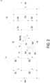
- FIG. 2 is a schematic circuit diagram illustrating a resonant converter according to an embodiment of the present disclosure.
- the resonant converter 1 of the present disclosure includes a switch circuit (for example but not limited to the full-bridge switch circuit 11 in FIG. 2 ), a resonant circuit 12, a transformer T, a rectifier circuit 13, a current sensor 14 and a controller 15.
- the switch circuit and the resonant circuit 12 form a primary circuit, and the rectifier circuit 13 forms a secondary circuit.
- the full-bridge switch circuit 11 includes a plurality of switches and receives an input voltage Vin.
- the resonant circuit 12 is electrically connected to the full-bridge switch circuit 11 and includes a resonant inductor Lr.
- a primary winding and a secondary winding of the transformer T are electrically connected to the resonant circuit 12 and the rectifier circuit 13 respectively, and the turns ratio of the primary and secondary windings is Np:Ns.
- the rectifier circuit 13 is configured to provide an output voltage Vo to a load L.
- the current sensor 14 is electrically connected to the resonant circuit 12. When a resonant current Ir flowing through the resonant inductor Lr passes through the current sensor 14, the current sensor 14 generates a current differential signal correspondingly.
- the current sensor 14 may include a coreless ring coil (e.g., Rogowski coil), but not limited thereto.
- the controller 15 is configured to perform double integration on the current differential signal generated by the current sensor 14 to obtain the electric charge signal Qcr.
- controller 15 controls the operation of the switches in the full-bridge switch circuit 11 according to the electric charge signal Qcr, the input voltage Vin and the output voltage Vo, thereby improving the dynamic response of the resonant converter 1 and eliminating the ripples of the output voltage Vo and output current.
- the full-bridge switch circuit 11 includes switches Q1, Q2, Q3 and Q4.
- the switches Q1 and Q2 are electrically connected in series to form a first bridge arm
- the switches Q3 and Q4 are electrically connected in series to form a second bridge arm
- the first bridge arm and the second bridge arm are electrically connected in parallel to each other.
- the resonant circuit 12 further includes a resonant capacitor Cr.
- Two terminals of the resonant inductor Lr are electrically connected to a connection node between switches Q1 and Q2 and a first terminal of the primary winding respectively.
- Two terminals of the resonant capacitor Cr are electrically connected to a connection node between switches Q3 and Q4 and a second terminal of the primary winding respectively.
- the current sensor 14 is electrically connected between the resonant capacitor Cr and the second terminal of the primary winding.
- the rectifier circuit 13 includes diodes D1, D2, D3 and D4.
- the diodes D1 and D2 are electrically connected in series to form a third bridge arm
- the diodes D3 and D4 are electrically connected in series to form a fourth bridge arm
- the third bridge arm and the fourth bridge arm are electrically connected in parallel to each other.
- a first terminal and a second terminal of the secondary winding of the transformer T are electrically connected to a connection node between diodes D1 and D2 and a connection node between diodes D3 and D4 respectively.
- the first terminal of the primary winding and the second terminal of the secondary winding are dotted terminals.
- the resonant converter 1 further includes an output capacitor Co electrically connected in parallel to the third and fourth bridge arms.
- a current sensing voltage Vsns can be obtained, and the current sensing voltage Vsns and the resonant current Ir have a relation as: Vsns ⁇ ⁇ ⁇ dIr
- Vsns ⁇ ⁇ Ir ⁇ ⁇ dVcr Vcr is the voltage across the resonant capacitor Cr.
- Vsns ⁇ Ksns ⁇ Vcr Ksns is a constant.
- FIG. 3 schematically shows the working waveforms of the resonant converter of FIG. 2 .
- Q1, Q2, Q3 and Q4 represent the control signals of switches Q1, Q2, Q3 and Q4 respectively.
- the electric charge signal Qcr obtained by the current sensor 14 and the double integration, has the same frequency and phase as the voltage Vcr across the resonant capacitor Cr.
- the approach of the present disclosure can avoid limiting the bandwidth and performing additional switching for sensing the signals in different half cycles and can obtain the required electric charge signal by simpler circuit structure.
- the controller 15 includes a double integrator circuit 151.
- the double integrator circuit 151 is electrically connected to the current sensor 14 for receiving the current differential signal, and the double integrator circuit 151 performs double integration on the current differential signal to acquire the electric charge signal Qcr.
- FIG. 4 exemplifies the circuit structure of the current sensor 14 and the double integrator circuit 151 of the controller 15.
- the double integrator circuit 151 includes resistors R1, R2, R3, R4 and R5, capacitors C1, C2 and C3, and a comparator Cmp.
- the current sensor 14 is a Rogowski coil, one terminal of the Rogowski coil is electrically connected to a first terminal of resistor R1, and the other terminal of the Rogowski coil is electrically connected to a first terminal of capacitor C1 and a reference voltage Vref.
- a second terminal of resistor R1 is connected to a second terminal of capacitor C1, and the resistor R1 and the capacitor C1 form a passive RC integrator.
- the resistor R2 is electrically connected between the second terminal of resistor R1 and a negative input terminal of comparator Cmp.
- the resistors R3 and R4 are electrically connected in series between a supply voltage Vcc and a ground terminal, and the connection node between resistors R3 and R4 is electrically connected to the positive input terminal of comparator Cmp.
- the capacitor C2 is electrically connected in parallel to the resistor R4.
- An output terminal of comparator Cmp outputs the electric charge signal Qcr.
- Two terminals of resistor R5 are electrically connected to the negative input terminal and the output terminal of the comparator Cmp respectively, and the capacitor C3 is electrically connected in parallel to the resistor R5.
- FIG. 5 schematically shows the control architecture of the controller 15 of FIG. 2 .
- the controller 15 includes the double integrator circuit 151, a voltage compensation circuit 152, a modulation circuit 153 and a driver 154.
- the modulation circuit 153 is electrically connected to the voltage compensation circuit 152, the double integrator circuit 151 and the driver 154.
- the voltage compensation circuit 152 generates an upper threshold voltage Vth_H according to the output voltage Vo and a reference output voltage Vo_ref.
- the modulation circuit 153 generates a modulation signal according to the input voltage Vin, the upper threshold voltage Vth_H and the electric charge signal Qcr.
- the driver 154 According to the modulation signal, the driver 154 generates the control signal utilized for controlling the operation of the switches in the full-bridge switch circuit 11.
- the voltage compensation circuit 152 includes a first operator 1521, a compensator 1522 and a limiter 1523 electrically connected to each other.
- the first operator 1521 calculates the difference between the output voltage Vo and the reference output voltage Vo_ref
- the compensator 1522 generates a compensation signal according to the difference
- the limiter 1523 generates the upper threshold voltage Vth_H according to the compensation signal.
- the modulation circuit 153 includes a second operator 1531, a first comparator 1532, a second comparator 1533 and a flip-flop 1534.
- the second operator 1531 calculates the difference between the input voltage Vin and the upper threshold voltage Vth_H, and the difference is regarded as a lower threshold voltage Vth_L.
- a positive input terminal and a negative input terminal of the first comparator 1532 receive the lower threshold voltage Vth_L and the upper threshold voltage Vth_H respectively.
- a positive input terminal and a negative input terminal of the second comparator 1533 receive the electric charge signal Qcr and the lower threshold voltage Vth_L respectively.
- An output terminal of the first comparator 1532 is electrically connected to the flip-flop 1534 for providing a first comparison signal to the flip-flop 1534.
- An output terminal of the second comparator 1533 is electrically connected to the flip-flop 1534 for providing a second comparison signal to the flip-flop 1534.
- the flip-flop 1534 generates the modulation signal according to the first comparison signal and the second comparison signal.
- the flip-flop 1534 includes an RS flip-flop, the R input terminal of the RS flip-flop is electrically connected to the output terminal of the first comparator 1532 for receiving the first comparison signal, and the S input terminal of the RS flip-flop is electrically connected to the output terminal of the second comparator 1533 for receiving the second comparison signal.
- FIG. 6 exemplifies a Bode plot of the closed-loop gain and phase in the case that the resonant converter 1 of FIG. 2 adopts the control architecture of present disclosure shown in FIG. 5 .
- FIG. 7 exemplifies a Bode plot of the closed-loop gain and phase in the case that the resonant converter 1 of FIG. 2 adopts the conventional control architecture of FIG. 1 .
- the waveforms of FIG. 6 and FIG. 7 are both obtained under the same conditions: the input voltage Vin of 400Vdc, the output voltage Vo of 300Vdc and the switching frequency fs of 440kHz. As shown in FIG. 6 and FIG.
- the bandwidth under the control architecture of the present disclosure is 1.3kHz while adopting the conventional control architecture, and the bandwidth is 13.6kHz while adopting the control architecture of the present disclosure. It is noted that the bandwidth under the control architecture of the present disclosure is ten times the bandwidth under the conventional control architecture. Therefore, with the same phase margin, the bandwidth under the control architecture of the present disclosure would be much larger than the bandwidth under the conventional control architecture. In other words, under the same stability condition, the control architecture of the present disclosure provides better dynamic response.
- the present disclosure provides a resonant converter.
- the electric charge signal is acquired by a current sensor disposed on a primary side and the double integration, and the operation of primary switches is controlled according to the electric charge signal and the input and output voltages of the resonant converter, thereby improving the dynamic response of the resonant converter and eliminating the ripples of the output voltage and current.
Landscapes
- Engineering & Computer Science (AREA)
- Power Engineering (AREA)
- Dc-Dc Converters (AREA)
Abstract
A resonant converter (1) including a full-bridge switch circuit (11), a resonant circuit (12), a transformer (T), a rectifier circuit (13), a current sensor (14) and a controller (15) is provided. The full-bridge switch circuit (11) includes switches (Q1, Q2, Q3, Q4). The resonant circuit (12) is electrically connected to the full-bridge switch circuit (11) and includes a resonant inductor (Lr). The transformer (T) includes primary and secondary windings, and the primary winding is electrically connected to the resonant circuit (12). The rectifier circuit (13) is electrically connected to the secondary winding. The current sensor (14) is electrically connected to the resonant circuit (12). When a current (Ir) flowing through the resonant inductor (Lr) passes through the current sensor (14), the current sensor (14) generates a current differential signal correspondingly. The controller (15) performs double integration on the current differential signal to acquire an electric charge signal (Qcr) and controls operation of the switches of the full-bridge switch circuit (11) according to the electric charge signal (Qcr) and the input and output voltages (Vin, Vo) of the resonant converter (1).
Description
- The present disclosure relates to a resonant converter, and more particularly to a resonant converter capable of improving the dynamic response.
- For full-bridge series resonant converters, the conventional control method adopts dual-loop control, as shown in
FIG. 1 . In the dual-loop control, the outer loop controls the voltage, the inner loop controls the current, and the control signal is generated through variable-frequency modulation. However, the bandwidth under the dual-loop control is small, which causes bad dynamic response. - In addition, in a conventional approach, the Rogowski coil is disposed on the secondary side to obtain a current differential signal, then an instantaneous current signal is acquired through integrating the current differential signal, and finally an average current signal is acquired by an average current controller accordingly. However, this conventional approach would limit the dynamic response of the converter and is unable to eliminate the ripples of the output voltage and current.
- Therefore, there is a need of providing a resonant converter in order to overcome the drawbacks of the conventional technologies.
- The present disclosure provides a resonant converter. In the resonant converter, the electric charge signal is acquired by a current sensor disposed on a primary side and the double integration, and the operation of primary switches is controlled according to the electric charge signal and the input and output voltages of the resonant converter, thereby improving the dynamic response of the resonant converter and eliminating the ripples of the output voltage and current.
- In accordance with an aspect of the present disclosure, a resonant converter is provided. The resonant converter includes a full-bridge switch circuit, a resonant circuit, a transformer, a rectifier circuit, a current sensor and a controller. The full-bridge switch circuit includes a plurality of switches and receives an input voltage. The resonant circuit is electrically connected to the full-bridge switch circuit and includes a resonant inductor. The transformer includes a primary winding and a secondary winding, and the primary winding is electrically connected to the resonant circuit. The rectifier circuit is electrically connected to the secondary winding of the transformer and provides an output voltage. The current sensor is electrically connected to the resonant circuit. When a current flowing through the resonant inductor passes through the current sensor, the current sensor generates a current differential signal correspondingly. The controller is configured to perform double integration on the current differential signal to acquire an electric charge signal, and to control operation of the plurality of switches of the full-bridge switch circuit according to the electric charge signal, the input voltage and the output voltage.
- In accordance with another aspect of the present disclosure, a resonant converter is provided. The resonant converter includes a primary circuit, a transformer, a secondary circuit, a current sensor and a controller. The primary circuit is configured to receive an input voltage includes a resonant inductor. The transformer has a primary side electrically connected to the primary circuit. The secondary circuit is electrically connected to a secondary side of the transformer and is configured to provide an output voltage. The current sensor is electrically connected to the primary circuit. When a current flowing through the resonant inductor passes through the current sensor, the current sensor generates a current differential signal correspondingly. The controller is configured to perform double integration on the current differential signal to acquire an electric charge signal, and is configured to control operation of the resonant converter according to the electric charge signal, the input voltage and the output voltage.
- In accordance with another aspect of the present disclosure, a resonant converter is provided. The resonant converter includes a switch circuit, a resonant circuit, a transformer, a rectifier circuit, a current sensor and a controller. The switch circuit includes a plurality of switches and receives an input voltage. The resonant circuit is electrically connected to the switch circuit. The transformer includes a primary winding and a secondary winding, and the primary winding is electrically connected to the resonant circuit. The rectifier circuit is electrically connected to the secondary winding of the transformer and provides an output voltage. The current sensor is electrically connected to the resonant circuit. When a current of the resonant circuit passes through the current sensor, the current sensor generates a current differential signal correspondingly. The controller is configured to perform double integration on the current differential signal to acquire an electric charge signal, and is configured to control operation of the plurality of switches of the switch circuit according to the electric charge signal, the input voltage and the output voltage.
-
-
FIG. 1 schematically shows the control architecture of a conventional dual-loop control for a full-bridge series resonant converter; -
FIG. 2 is a schematic circuit diagram illustrating a resonant converter according to an embodiment of the present disclosure; -
FIG. 3 schematically shows the working waveforms of the resonant converter ofFIG. 2 ; -
FIG. 4 is a schematic circuit diagram illustrating the current sensor and the double integrator circuit of the controller of the resonant converter ofFIG. 2 ; -
FIG. 5 schematically shows the control architecture of the controller ofFIG. 2 ; -
FIG. 6 exemplifies a Bode plot of the closed-loop gain and phase in the case that the resonant converter ofFIG. 2 adopts the control architecture of present disclosure shown inFIG. 5 ; and -
FIG. 7 exemplifies a Bode plot of the closed-loop gain and phase in the case that the resonant converter ofFIG. 2 adopts the conventional control architecture ofFIG. 1 - The present disclosure will now be described more specifically with reference to the following embodiments. It is to be noted that the following descriptions of preferred embodiments of this disclosure are presented herein for purpose of illustration and description only. It is not intended to be exhaustive or to be limited to the precise form disclosed.
-
FIG. 2 is a schematic circuit diagram illustrating a resonant converter according to an embodiment of the present disclosure. As shown inFIG. 2 , theresonant converter 1 of the present disclosure includes a switch circuit (for example but not limited to the full-bridge switch circuit 11 inFIG. 2 ), aresonant circuit 12, a transformer T, arectifier circuit 13, acurrent sensor 14 and acontroller 15. The switch circuit and theresonant circuit 12 form a primary circuit, and therectifier circuit 13 forms a secondary circuit. The full-bridge switch circuit 11 includes a plurality of switches and receives an input voltage Vin. Theresonant circuit 12 is electrically connected to the full-bridge switch circuit 11 and includes a resonant inductor Lr. A primary winding and a secondary winding of the transformer T are electrically connected to theresonant circuit 12 and therectifier circuit 13 respectively, and the turns ratio of the primary and secondary windings is Np:Ns. Therectifier circuit 13 is configured to provide an output voltage Vo to a load L. Thecurrent sensor 14 is electrically connected to theresonant circuit 12. When a resonant current Ir flowing through the resonant inductor Lr passes through thecurrent sensor 14, thecurrent sensor 14 generates a current differential signal correspondingly. Thecurrent sensor 14 may include a coreless ring coil (e.g., Rogowski coil), but not limited thereto. Thecontroller 15 is configured to perform double integration on the current differential signal generated by thecurrent sensor 14 to obtain the electric charge signal Qcr. Further, thecontroller 15 controls the operation of the switches in the full-bridge switch circuit 11 according to the electric charge signal Qcr, the input voltage Vin and the output voltage Vo, thereby improving the dynamic response of theresonant converter 1 and eliminating the ripples of the output voltage Vo and output current. - In an embodiment, the full-
bridge switch circuit 11 includes switches Q1, Q2, Q3 and Q4. The switches Q1 and Q2 are electrically connected in series to form a first bridge arm, the switches Q3 and Q4 are electrically connected in series to form a second bridge arm, and the first bridge arm and the second bridge arm are electrically connected in parallel to each other. - In an embodiment, the
resonant circuit 12 further includes a resonant capacitor Cr. Two terminals of the resonant inductor Lr are electrically connected to a connection node between switches Q1 and Q2 and a first terminal of the primary winding respectively. Two terminals of the resonant capacitor Cr are electrically connected to a connection node between switches Q3 and Q4 and a second terminal of the primary winding respectively. Thecurrent sensor 14 is electrically connected between the resonant capacitor Cr and the second terminal of the primary winding. - In an embodiment, the
rectifier circuit 13 includes diodes D1, D2, D3 and D4. The diodes D1 and D2 are electrically connected in series to form a third bridge arm, the diodes D3 and D4 are electrically connected in series to form a fourth bridge arm, and the third bridge arm and the fourth bridge arm are electrically connected in parallel to each other. A first terminal and a second terminal of the secondary winding of the transformer T are electrically connected to a connection node between diodes D1 and D2 and a connection node between diodes D3 and D4 respectively. In the transformer T, the first terminal of the primary winding and the second terminal of the secondary winding are dotted terminals. In an embodiment, theresonant converter 1 further includes an output capacitor Co electrically connected in parallel to the third and fourth bridge arms. - Moreover, based on the sensing result of the
current sensor 14, a current sensing voltage Vsns can be obtained, and the current sensing voltage Vsns and the resonant current Ir have a relation as:
- It may be further derived that:


-
FIG. 3 schematically shows the working waveforms of the resonant converter ofFIG. 2 . InFIG. 3 , Q1, Q2, Q3 and Q4 represent the control signals of switches Q1, Q2, Q3 and Q4 respectively. As shown inFIG. 3 , the electric charge signal Qcr, obtained by thecurrent sensor 14 and the double integration, has the same frequency and phase as the voltage Vcr across the resonant capacitor Cr. Compared to the conventional approach in which the electric charge signal is obtained through sensing the voltage across the resonant capacitor by an isolated operational amplifier, the approach of the present disclosure can avoid limiting the bandwidth and performing additional switching for sensing the signals in different half cycles and can obtain the required electric charge signal by simpler circuit structure. - In an embodiment, as shown in
FIG. 2 , thecontroller 15 includes adouble integrator circuit 151. Thedouble integrator circuit 151 is electrically connected to thecurrent sensor 14 for receiving the current differential signal, and thedouble integrator circuit 151 performs double integration on the current differential signal to acquire the electric charge signal Qcr.FIG. 4 exemplifies the circuit structure of thecurrent sensor 14 and thedouble integrator circuit 151 of thecontroller 15. In an embodiment, as shown inFIG. 4 , thedouble integrator circuit 151 includes resistors R1, R2, R3, R4 and R5, capacitors C1, C2 and C3, and a comparator Cmp. In this embodiment, thecurrent sensor 14 is a Rogowski coil, one terminal of the Rogowski coil is electrically connected to a first terminal of resistor R1, and the other terminal of the Rogowski coil is electrically connected to a first terminal of capacitor C1 and a reference voltage Vref. A second terminal of resistor R1 is connected to a second terminal of capacitor C1, and the resistor R1 and the capacitor C1 form a passive RC integrator. The resistor R2 is electrically connected between the second terminal of resistor R1 and a negative input terminal of comparator Cmp. The resistors R3 and R4 are electrically connected in series between a supply voltage Vcc and a ground terminal, and the connection node between resistors R3 and R4 is electrically connected to the positive input terminal of comparator Cmp. The capacitor C2 is electrically connected in parallel to the resistor R4. An output terminal of comparator Cmp outputs the electric charge signal Qcr. Two terminals of resistor R5 are electrically connected to the negative input terminal and the output terminal of the comparator Cmp respectively, and the capacitor C3 is electrically connected in parallel to the resistor R5. -
FIG. 5 schematically shows the control architecture of thecontroller 15 ofFIG. 2 . In an embodiment, as shown inFIG. 5 , thecontroller 15 includes thedouble integrator circuit 151, avoltage compensation circuit 152, amodulation circuit 153 and adriver 154. Themodulation circuit 153 is electrically connected to thevoltage compensation circuit 152, thedouble integrator circuit 151 and thedriver 154. Thevoltage compensation circuit 152 generates an upper threshold voltage Vth_H according to the output voltage Vo and a reference output voltage Vo_ref. Themodulation circuit 153 generates a modulation signal according to the input voltage Vin, the upper threshold voltage Vth_H and the electric charge signal Qcr. According to the modulation signal, thedriver 154 generates the control signal utilized for controlling the operation of the switches in the full-bridge switch circuit 11. - In this embodiment, the
voltage compensation circuit 152 includes afirst operator 1521, acompensator 1522 and alimiter 1523 electrically connected to each other. Thefirst operator 1521 calculates the difference between the output voltage Vo and the reference output voltage Vo_ref, thecompensator 1522 generates a compensation signal according to the difference, and thelimiter 1523 generates the upper threshold voltage Vth_H according to the compensation signal. - The
modulation circuit 153 includes asecond operator 1531, afirst comparator 1532, asecond comparator 1533 and a flip-flop 1534. Thesecond operator 1531 calculates the difference between the input voltage Vin and the upper threshold voltage Vth_H, and the difference is regarded as a lower threshold voltage Vth_L. A positive input terminal and a negative input terminal of thefirst comparator 1532 receive the lower threshold voltage Vth_L and the upper threshold voltage Vth_H respectively. A positive input terminal and a negative input terminal of thesecond comparator 1533 receive the electric charge signal Qcr and the lower threshold voltage Vth_L respectively. An output terminal of thefirst comparator 1532 is electrically connected to the flip-flop 1534 for providing a first comparison signal to the flip-flop 1534. An output terminal of thesecond comparator 1533 is electrically connected to the flip-flop 1534 for providing a second comparison signal to the flip-flop 1534. The flip-flop 1534 generates the modulation signal according to the first comparison signal and the second comparison signal. In an embodiment, the flip-flop 1534 includes an RS flip-flop, the R input terminal of the RS flip-flop is electrically connected to the output terminal of thefirst comparator 1532 for receiving the first comparison signal, and the S input terminal of the RS flip-flop is electrically connected to the output terminal of thesecond comparator 1533 for receiving the second comparison signal. -
FIG. 6 exemplifies a Bode plot of the closed-loop gain and phase in the case that theresonant converter 1 ofFIG. 2 adopts the control architecture of present disclosure shown inFIG. 5 .FIG. 7 exemplifies a Bode plot of the closed-loop gain and phase in the case that theresonant converter 1 ofFIG. 2 adopts the conventional control architecture ofFIG. 1 . The waveforms ofFIG. 6 andFIG. 7 are both obtained under the same conditions: the input voltage Vin of 400Vdc, the output voltage Vo of 300Vdc and the switching frequency fs of 440kHz. As shown inFIG. 6 andFIG. 7 , with the phase margin of 60 degrees, the bandwidth is 1.3kHz while adopting the conventional control architecture, and the bandwidth is 13.6kHz while adopting the control architecture of the present disclosure. It is noted that the bandwidth under the control architecture of the present disclosure is ten times the bandwidth under the conventional control architecture. Therefore, with the same phase margin, the bandwidth under the control architecture of the present disclosure would be much larger than the bandwidth under the conventional control architecture. In other words, under the same stability condition, the control architecture of the present disclosure provides better dynamic response. - In summary, the present disclosure provides a resonant converter. In the resonant converter, the electric charge signal is acquired by a current sensor disposed on a primary side and the double integration, and the operation of primary switches is controlled according to the electric charge signal and the input and output voltages of the resonant converter, thereby improving the dynamic response of the resonant converter and eliminating the ripples of the output voltage and current.
Claims (15)
- A resonant converter (1), characterized by comprising:a full-bridge switch circuit (11), comprising a plurality of switches (Q1, Q2, Q3, Q4), and receiving an input voltage (Vin);a resonant circuit (12), electrically connected to the full-bridge switch circuit (11), and comprising a resonant inductor (Lr);a transformer (T), comprising a primary winding and a secondary winding, wherein the primary winding is electrically connected to the resonant circuit (12);a rectifier circuit (13), electrically connected to the secondary winding of the transformer (T), and providing an output voltage (Vo);a current sensor (14), electrically connected to the resonant circuit (12), wherein when a current (Ir) flowing through the resonant inductor (Lr) passes through the current sensor (14), the current sensor (14) generates a current differential signal correspondingly; anda controller (15), configured to perform double integration on the current differential signal to acquire an electric charge signal (Qcr), and configured to control operation of the plurality of switches of the full-bridge switch circuit (11) according to the electric charge signal (Qcr), the input voltage (Vin) and the output voltage (Vo).
- The resonant converter (1) according to claim 1, wherein the resonant circuit (12) further comprises a resonant capacitor (Cr), the resonant inductor (Lr) and the resonant capacitor (Cr) are electrically connected to two terminals of the primary winding respectively, and the current sensor (14) is electrically connected between the resonant capacitor (Cr) and the primary winding.
- The resonant converter (1) according to claim 1, wherein the controller (15) comprises a double integrator circuit (151) electrically connected to the current sensor (14) for receiving the current differential signal, and the double integrator circuit (151) performs the double integration on the current differential signal to acquire the electric charge signal (Qcr).
- The resonant converter (1) according to claim 3, wherein the controller (15) further comprises a voltage compensation circuit (152), a modulation circuit (153) and a driver (154), the modulation circuit (153) is electrically connected to the voltage compensation circuit (152), the double integrator circuit (151) and the driver (154), the voltage compensation circuit (152) generates an upper threshold voltage (Vth_H) according to the output voltage (Vo) and a reference output voltage (Vo_ref), the modulation circuit (153) generates a modulation signal according to the input voltage (Vin), the upper threshold voltage (Vth_H) and the electric charge signal (Qcr), the driver (154) generates a control signal according to the modulation signal, and the control signal is utilized to control the operation of the plurality of switches of the full-bridge switch circuit (11).
- The resonant converter (1) according to claim 4, wherein the voltage compensation circuit (152) comprises a first operator (1521), a compensator (1522) and a limiter (1523) electrically connected to each other, the first operator (1521) calculates a difference between the output voltage (Vo) and the reference output voltage (Vo_ref), the compensator (1522) generates a compensation signal according to the difference, and the limiter (1523) generates the upper threshold voltage (Vth_H) according to the compensation signal.
- The resonant converter (1) according to claim 4, wherein the modulation circuit (153) comprises a second operator (1531), a first comparator (1532), a second comparator (1533) and a flip-flop (1534), the second operator (1531) calculates a difference between the input voltage (Vin) and the upper threshold voltage (Vth_H), the difference is regarded as a lower threshold voltage (Vth_L), a positive input terminal and a negative input terminal of the first comparator (1532) receive the lower threshold voltage (Vth_L) and the upper threshold voltage (Vth_H) respectively, a positive input terminal and a negative input terminal of the second comparator (1533) receive the electric charge signal (Qcr) and the lower threshold voltage (Vth_L) respectively, the first comparator (1532) and the second comparator (1533) outputs a first comparison signal and a second comparison signal to the flip-flop (1534) respectively, and the flip-flop (1534) generates the modulation signal according to the first comparison signal and the second comparison signal.
- The resonant converter (1) according to claim 6, wherein the flip-flop (1534) comprises an RS flip-flop, an R input terminal and an S input terminal of the RS flip-flop receive the first comparison signal and the second comparison signal respectively
- The resonant converter (1) according to claim 1, wherein the plurality of switches of the full-bridge switch circuit (11) comprises a first switch (Q 1), a second switch (Q2), a third switch (Q3) and a fourth switch (Q4), a first bridge arm formed by the first switch (Q1) and the second switch (Q2) electrically connected in series is electrically connected in parallel to a second bridge arm formed by the third switch (Q3) and the fourth switch (Q4) electrically connected in series, and a connection node between the first switch (Q1) and the second switch (Q2) and a connection node between the third switch (Q3) and the fourth switch (Q4) are electrically connected to two terminals of the primary winding respectively.
- The resonant converter (1) according to claim 1, wherein the rectifier circuit (13) comprises a first diode (D1), a second diode (D2), a third diode (D3) and a fourth diode (D4), a third bridge arm formed by the first diode (D1) and the second diode (D2) electrically connected in series is electrically connected in parallel to a fourth bridge arm formed by the third diode (D3) and the fourth diode (D4) electrically connected in series, and a connection node between the first diode (D1) and the second diode (D2) and a connection node between the third diode (D3) and the fourth diode (D4) are electrically connected to two terminals of the secondary winding respectively.
- A resonant converter (1), characterized by comprising:a primary circuit, configured to receive an input voltage (Vin), and comprising a resonant inductor (Lr);a transformer (T), having a primary side electrically connected to the primary circuit;a secondary circuit, electrically connected to a secondary side of the transformer (T), and configured to provide an output voltage (Vo);a current sensor (14), electrically connected to the primary circuit, wherein when a current (Ir) flowing through the resonant inductor (Lr) passes through the current sensor (14), the current sensor (14) generates a current differential signal correspondingly; anda controller (15), configured to perform double integration on the current differential signal to acquire an electric charge signal (Qcr), and configured to control operation of the resonant converter (1) according to the electric charge signal (Qcr), the input voltage (Vin) and the output voltage (Vo).
- The resonant converter (1) according to claim 10, wherein the primary circuit further comprises a resonant capacitor (Cr) electrically connected to the resonant inductor (Lr), and the current sensor (14) is electrically connected to the resonant capacitor (Cr).
- A resonant converter (1), characterized by comprising:a switch circuit (11), comprising a plurality of switches, and receiving an input voltage (Vin);a resonant circuit (12), electrically connected to the switch circuit (11);a transformer (T), comprising a primary winding and a secondary winding, wherein the primary winding is electrically connected to the resonant circuit (12);a rectifier circuit (13), electrically connected to the secondary winding of the transformer (T), and providing an output voltage (Vo);a current sensor (14), electrically connected to the resonant circuit (12), wherein when a current (Ir) of the resonant circuit (12) passes through the current sensor (14), the current sensor (14) generates a current differential signal correspondingly; anda controller (15), configured to perform double integration on the current differential signal to acquire an electric charge signal (Qcr), and configured to control operation of the plurality of switches of the switch circuit (11) according to the electric charge signal (Qcr), the input voltage (Vin) and the output voltage (Vo).
- The resonant converter (1) according to claim 12, wherein the resonant circuit (12) comprises a resonant inductor (Lr) and a resonant capacitor (Cr) electrically connected to two terminals of the primary winding respectively, and the current sensor (14) is electrically connected between the resonant capacitor (Cr) and the primary winding.
- The resonant converter (1) according to any of claims 2, 11 and 13, wherein the electrical charge signal (Qcr) and a voltage (Vcr) across the resonant capacitor (Cr) have same frequency and phase.
- The resonant converter (1) according to any of claims 1, 10 and 12, wherein the current sensor (14) comprises a coreless ring coil, and the coreless ring coil comprises a Rogowski coil.
Applications Claiming Priority (1)
| Application Number | Priority Date | Filing Date | Title |
|---|---|---|---|
| CN202310642753.1A CN119070642A (en) | 2023-06-01 | 2023-06-01 | Resonant Converter |
Publications (1)
| Publication Number | Publication Date |
|---|---|
| EP4472046A1 true EP4472046A1 (en) | 2024-12-04 |
Family
ID=88291218
Family Applications (1)
| Application Number | Title | Priority Date | Filing Date |
|---|---|---|---|
| EP23201787.1A Pending EP4472046A1 (en) | 2023-06-01 | 2023-10-05 | Resonant converter |
Country Status (3)
| Country | Link |
|---|---|
| US (1) | US12592635B2 (en) |
| EP (1) | EP4472046A1 (en) |
| CN (1) | CN119070642A (en) |
Citations (1)
| Publication number | Priority date | Publication date | Assignee | Title |
|---|---|---|---|---|
| US20220286056A1 (en) * | 2021-03-03 | 2022-09-08 | Semiconductor Components Industries, Llc | Resonant converter with dual-mode control |
Family Cites Families (11)
| Publication number | Priority date | Publication date | Assignee | Title |
|---|---|---|---|---|
| EP2811638B1 (en) | 2012-02-03 | 2017-12-20 | Fuji Electric Co., Ltd. | Control device for resonance-type dc-dc converter |
| JP6272036B2 (en) | 2013-02-13 | 2018-01-31 | 株式会社Soken | Power converter |
| US11437917B2 (en) | 2019-07-25 | 2022-09-06 | Texas Instruments Incorporated | Predictive synchronous rectifier sensing and control |
| CN111983282A (en) | 2020-08-20 | 2020-11-24 | 青岛鼎信通讯股份有限公司 | Detection circuit applied to power electronic transformer power module resonant current |
| EP4002668A1 (en) * | 2020-11-13 | 2022-05-25 | Siemens Aktiengesellschaft | Method and circuit for regulating a resonant converter |
| CN113189392B (en) | 2021-04-28 | 2023-02-17 | 河北工业大学 | PCB Rogowski coil current sensor for measuring switch current |
| CN113394985B (en) | 2021-07-21 | 2022-08-23 | 矽力杰半导体技术(杭州)有限公司 | Control circuit, resonant converter and integrated circuit control chip |
| US11791733B2 (en) * | 2021-09-23 | 2023-10-17 | Delta Electronics, Inc. | Isolated resonant DC-DC converters and control methods thereof |
| US11799387B2 (en) * | 2021-10-27 | 2023-10-24 | Infineon Technologies Austria Ag | Synchronous rectifier controller and related sensing circuitry for series-parallel resonant converters |
| CN113744608B (en) | 2021-11-08 | 2022-02-08 | 西南交通大学 | Non-contact micro current measuring system based on Rogowski coil |
| CN115833605A (en) | 2022-12-13 | 2023-03-21 | 无锡格兰德微电子科技有限公司 | Dead time self-adaptive adjusting circuit of resonant switch controller |
-
2023
- 2023-06-01 CN CN202310642753.1A patent/CN119070642A/en active Pending
- 2023-09-18 US US18/369,747 patent/US12592635B2/en active Active
- 2023-10-05 EP EP23201787.1A patent/EP4472046A1/en active Pending
Patent Citations (1)
| Publication number | Priority date | Publication date | Assignee | Title |
|---|---|---|---|---|
| US20220286056A1 (en) * | 2021-03-03 | 2022-09-08 | Semiconductor Components Industries, Llc | Resonant converter with dual-mode control |
Non-Patent Citations (2)
| Title |
|---|
| "Power Electronics Design : A Practitioner's Guide", 21 September 2005, ELSEVIER SCIENCE & TECHNOLOGY, ISBN: 978-1-4933-0316-8, article SUEKER KEITH H.: "Rogowski Coils", pages: 237 - 238, XP093137941 * |
| HU ZHIYUAN ET AL: "Bang-Bang Charge Control for LLC Resonant Conver", IEEE TRANSACTIONS ON POWER ELECTRONICS, INSTITUTE OF ELECTRICAL AND ELECTRONICS ENGINEERS, USA, vol. 30, no. 2, February 2015 (2015-02-01), pages 1093 - 1108, XP011560839, ISSN: 0885-8993, [retrieved on 20141007], DOI: 10.1109/TPEL.2014.2313130 * |
Also Published As
| Publication number | Publication date |
|---|---|
| US12592635B2 (en) | 2026-03-31 |
| US20240405687A1 (en) | 2024-12-05 |
| CN119070642A (en) | 2024-12-03 |
Similar Documents
| Publication | Publication Date | Title |
|---|---|---|
| US10715048B2 (en) | Controller and control method used in resonant converters | |
| US7446512B2 (en) | Resonant switching power supply device | |
| US11005378B2 (en) | Operating a flyback converter using a signal indicative of a resonant tank current of the flyback converter | |
| US6396716B1 (en) | Apparatus for improving stability and dynamic response of half-bridge converter | |
| JP3198944B2 (en) | Switching power supply | |
| US6127814A (en) | System to protect switch mode DC/DC converters against overload current | |
| US8891255B2 (en) | Switching power supply apparatus including simultanous control of multiple outputs | |
| US8536841B2 (en) | PWM control circuit of a converter and the control method thereof | |
| US20230412085A1 (en) | Isolated resonant dc-dc converter | |
| US8149601B2 (en) | Adaptive slope compensation method for stabilizing a continuous conduction mode converter | |
| CN112366954B (en) | Resonant converter, controller and control method thereof | |
| TWI590574B (en) | Power supply apparatus | |
| CN112019054B (en) | Opto-coupler current transfer ratio compensation | |
| US9190918B2 (en) | Controllers and related control methods for generating signals representing an output current to a load in a switched mode power supply | |
| US20130057234A1 (en) | Control methods and power controllers with load compensation adapted for a power supply | |
| US10483860B1 (en) | Primary side constant current regulation | |
| US10177663B2 (en) | DC-DC converting circuit and multi-phase power controller thereof | |
| US20240413732A1 (en) | Trans-inductor voltage regulator with average current sensing and correction | |
| KR20220092510A (en) | Digital Non-Linear Conversion for Voltage Mode Control of Power Converters | |
| JP3465682B2 (en) | Switching power supply | |
| JP2001008452A (en) | Power supply device | |
| US12592635B2 (en) | Resonant converter | |
| US20050169023A1 (en) | Switching power supply using controlled negative feedback in series with a switching device and responsive to the voltage and/or current to a load | |
| TWI867562B (en) | Resonant converter | |
| US11848607B2 (en) | Simple constant current limit for SEPIC or boost converter |
Legal Events
| Date | Code | Title | Description |
|---|---|---|---|
| PUAI | Public reference made under article 153(3) epc to a published international application that has entered the european phase |
Free format text: ORIGINAL CODE: 0009012 |
|
| STAA | Information on the status of an ep patent application or granted ep patent |
Free format text: STATUS: THE APPLICATION HAS BEEN PUBLISHED |
|
| AK | Designated contracting states |
Kind code of ref document: A1 Designated state(s): AL AT BE BG CH CY CZ DE DK EE ES FI FR GB GR HR HU IE IS IT LI LT LU LV MC ME MK MT NL NO PL PT RO RS SE SI SK SM TR |
|
| STAA | Information on the status of an ep patent application or granted ep patent |
Free format text: STATUS: REQUEST FOR EXAMINATION WAS MADE |
|
| 17P | Request for examination filed |
Effective date: 20250221 |