EP4472017A1 - Power supply circuit, electronic apparatus, and control method - Google Patents
Power supply circuit, electronic apparatus, and control method Download PDFInfo
- Publication number
- EP4472017A1 EP4472017A1 EP24166466.3A EP24166466A EP4472017A1 EP 4472017 A1 EP4472017 A1 EP 4472017A1 EP 24166466 A EP24166466 A EP 24166466A EP 4472017 A1 EP4472017 A1 EP 4472017A1
- Authority
- EP
- European Patent Office
- Prior art keywords
- charging
- voltage
- battery
- power
- power supply
- Prior art date
- Legal status (The legal status is an assumption and is not a legal conclusion. Google has not performed a legal analysis and makes no representation as to the accuracy of the status listed.)
- Granted
Links
Images



Classifications
-
- H—ELECTRICITY
- H02—GENERATION; CONVERSION OR DISTRIBUTION OF ELECTRIC POWER
- H02J—ELECTRIC POWER NETWORKS; CIRCUIT ARRANGEMENTS OR SYSTEMS FOR SUPPLYING OR DISTRIBUTING ELECTRIC POWER; SYSTEMS FOR STORING ELECTRIC ENERGY
- H02J7/00—Circuit arrangements for charging or discharging batteries or for supplying loads from batteries
- H02J7/02—Circuit arrangements for charging or discharging batteries or for supplying loads from batteries for charging batteries from AC mains by converters
- H02J7/04—Regulation of charging current or voltage
- H02J7/06—Regulation of charging current or voltage using discharge tubes or semiconductor devices
-
- H—ELECTRICITY
- H02—GENERATION; CONVERSION OR DISTRIBUTION OF ELECTRIC POWER
- H02J—ELECTRIC POWER NETWORKS; CIRCUIT ARRANGEMENTS OR SYSTEMS FOR SUPPLYING OR DISTRIBUTING ELECTRIC POWER; SYSTEMS FOR STORING ELECTRIC ENERGY
- H02J7/00—Circuit arrangements for charging or discharging batteries or for supplying loads from batteries
- H02J7/90—Regulation of charging or discharging current or voltage
- H02J7/933—Regulation of charging or discharging current or voltage the cycle being controlled or terminated in response to electric parameters
-
- H—ELECTRICITY
- H02—GENERATION; CONVERSION OR DISTRIBUTION OF ELECTRIC POWER
- H02J—ELECTRIC POWER NETWORKS; CIRCUIT ARRANGEMENTS OR SYSTEMS FOR SUPPLYING OR DISTRIBUTING ELECTRIC POWER; SYSTEMS FOR STORING ELECTRIC ENERGY
- H02J7/00—Circuit arrangements for charging or discharging batteries or for supplying loads from batteries
- H02J7/865—Battery or charger load switching, e.g. concurrent charging and load supply
-
- H—ELECTRICITY
- H01—ELECTRIC ELEMENTS
- H01M—PROCESSES OR MEANS, e.g. BATTERIES, FOR THE DIRECT CONVERSION OF CHEMICAL ENERGY INTO ELECTRICAL ENERGY
- H01M10/00—Secondary cells; Manufacture thereof
- H01M10/42—Methods or arrangements for servicing or maintenance of secondary cells or secondary half-cells
- H01M10/44—Methods for charging or discharging
-
- H—ELECTRICITY
- H02—GENERATION; CONVERSION OR DISTRIBUTION OF ELECTRIC POWER
- H02H—EMERGENCY PROTECTIVE CIRCUIT ARRANGEMENTS
- H02H3/00—Emergency protective circuit arrangements for automatic disconnection directly responsive to an undesired change from normal electric working condition with or without subsequent reconnection ; integrated protection
- H02H3/08—Emergency protective circuit arrangements for automatic disconnection directly responsive to an undesired change from normal electric working condition with or without subsequent reconnection ; integrated protection responsive to excess current
- H02H3/087—Emergency protective circuit arrangements for automatic disconnection directly responsive to an undesired change from normal electric working condition with or without subsequent reconnection ; integrated protection responsive to excess current for DC applications
-
- H—ELECTRICITY
- H02—GENERATION; CONVERSION OR DISTRIBUTION OF ELECTRIC POWER
- H02H—EMERGENCY PROTECTIVE CIRCUIT ARRANGEMENTS
- H02H7/00—Emergency protective circuit arrangements specially adapted for specific types of electric machines or apparatus or for sectionalised protection of cable or line systems, and effecting automatic switching in the event of an undesired change from normal working conditions
- H02H7/18—Emergency protective circuit arrangements specially adapted for specific types of electric machines or apparatus or for sectionalised protection of cable or line systems, and effecting automatic switching in the event of an undesired change from normal working conditions for batteries; for accumulators
-
- H—ELECTRICITY
- H02—GENERATION; CONVERSION OR DISTRIBUTION OF ELECTRIC POWER
- H02J—ELECTRIC POWER NETWORKS; CIRCUIT ARRANGEMENTS OR SYSTEMS FOR SUPPLYING OR DISTRIBUTING ELECTRIC POWER; SYSTEMS FOR STORING ELECTRIC ENERGY
- H02J7/00—Circuit arrangements for charging or discharging batteries or for supplying loads from batteries
- H02J7/60—Circuit arrangements for charging or discharging batteries or for supplying loads from batteries including safety or protection arrangements
- H02J7/62—Circuit arrangements for charging or discharging batteries or for supplying loads from batteries including safety or protection arrangements against overcurrent
-
- H—ELECTRICITY
- H02—GENERATION; CONVERSION OR DISTRIBUTION OF ELECTRIC POWER
- H02J—ELECTRIC POWER NETWORKS; CIRCUIT ARRANGEMENTS OR SYSTEMS FOR SUPPLYING OR DISTRIBUTING ELECTRIC POWER; SYSTEMS FOR STORING ELECTRIC ENERGY
- H02J7/00—Circuit arrangements for charging or discharging batteries or for supplying loads from batteries
- H02J7/80—Circuit arrangements for charging or discharging batteries or for supplying loads from batteries including monitoring or indicating arrangements
- H02J7/82—Control of state of charge [SOC]
-
- H—ELECTRICITY
- H02—GENERATION; CONVERSION OR DISTRIBUTION OF ELECTRIC POWER
- H02J—ELECTRIC POWER NETWORKS; CIRCUIT ARRANGEMENTS OR SYSTEMS FOR SUPPLYING OR DISTRIBUTING ELECTRIC POWER; SYSTEMS FOR STORING ELECTRIC ENERGY
- H02J7/00—Circuit arrangements for charging or discharging batteries or for supplying loads from batteries
- H02J7/80—Circuit arrangements for charging or discharging batteries or for supplying loads from batteries including monitoring or indicating arrangements
- H02J7/82—Control of state of charge [SOC]
- H02J7/825—Detection of fully charged condition
-
- H—ELECTRICITY
- H02—GENERATION; CONVERSION OR DISTRIBUTION OF ELECTRIC POWER
- H02J—ELECTRIC POWER NETWORKS; CIRCUIT ARRANGEMENTS OR SYSTEMS FOR SUPPLYING OR DISTRIBUTING ELECTRIC POWER; SYSTEMS FOR STORING ELECTRIC ENERGY
- H02J7/00—Circuit arrangements for charging or discharging batteries or for supplying loads from batteries
- H02J7/90—Regulation of charging or discharging current or voltage
- H02J7/96—Regulation of charging or discharging current or voltage in response to battery voltage
-
- G—PHYSICS
- G06—COMPUTING OR CALCULATING; COUNTING
- G06F—ELECTRIC DIGITAL DATA PROCESSING
- G06F1/00—Details not covered by groups G06F3/00 - G06F13/00 and G06F21/00
- G06F1/26—Power supply means, e.g. regulation thereof
- G06F1/263—Arrangements for using multiple switchable power supplies, e.g. battery and AC
-
- Y—GENERAL TAGGING OF NEW TECHNOLOGICAL DEVELOPMENTS; GENERAL TAGGING OF CROSS-SECTIONAL TECHNOLOGIES SPANNING OVER SEVERAL SECTIONS OF THE IPC; TECHNICAL SUBJECTS COVERED BY FORMER USPC CROSS-REFERENCE ART COLLECTIONS [XRACs] AND DIGESTS
- Y02—TECHNOLOGIES OR APPLICATIONS FOR MITIGATION OR ADAPTATION AGAINST CLIMATE CHANGE
- Y02E—REDUCTION OF GREENHOUSE GAS [GHG] EMISSIONS, RELATED TO ENERGY GENERATION, TRANSMISSION OR DISTRIBUTION
- Y02E60/00—Enabling technologies; Technologies with a potential or indirect contribution to GHG emissions mitigation
- Y02E60/10—Energy storage using batteries
Definitions
- the present invention relates to a power supply circuit, an electronic apparatus, and a control method related, for example, to battery charging.
- Battery packs may be equipped in information apparatuses, such as PCs (Personal Computers), tablet terminals, smartphones, and other various electronic apparatuses.
- An electronic apparatus is operable by consuming electric power charged in a battery pack even when no electric power is supplied from outside.
- a battery secondary battery
- AC Alternating Current
- a power supply circuit which is a system charging IC (Integrated Circuit), for example.
- a charging method disclosed in Japanese Unexamined Patent Application Publication No. H04-183232 is a charging method for a secondary battery to further charge the secondary battery for a certain period of time after charging of the secondary battery deviates from a predetermined condition in a method for charging the secondary battery by a constant voltage power supply with current limited.
- the predetermined condition is that the battery voltage of the secondary battery becomes a predetermined voltage or the charging current of the secondary battery becomes a predetermined current.
- system non-operating charge also called system off charge or off charge
- system operating charge also called system operation charge or on charge
- the system non-operating charge is a method for charging only the battery without supplying electric power to the system.
- the system operating charge is a method for charging the battery as well while supplying electric power to the system. In the system non-operating charge, almost all of supply current I total supplied from the AC adapter is charged to the battery.
- a controller determines that the charged state of the battery has reached a fully charged state, and charging is finished.
- a required current out of the supplied charging current I total is supplied to the system as a system current I sys .
- a residual current I total -I sys after removing, from the supply current I total the system current I sys supplied to the system is supplied to the battery. Therefore, the supplied current may not meet the battery requirements.
- a decrease in charging power to be charged to the battery may become noticeable. Under such circumstances, even when the conditions that the cell voltage becomes the taper voltage or more and the charging current becomes the taper current or less are met, the capacity of electric charge stored in the battery may become smaller than the capacity in the fully charged state (full charge capacity) originally expected.
- a voltage lower by a given margin than the rated value of a system voltage supplied from the system is set as the taper voltage.
- the charge capacity stored in the battery may be lower than the full charge capacity.
- the taper voltage depends on circuit resistance values of the battery and the system, but these circuit resistance values vary individually. In order to ensure safety or stability, a larger margin than necessary tends to be set on each individual equipment by taking individual differences into account at the design stage.
- a power supply circuit supplies, to a system, system power required for the system out of DC power supplied from a power supply, and charges a battery with charging power as the remaining power, and when a cell voltage of the battery is a predetermined detection voltage or more and a charging current of the charging power becomes a predetermined detection current or less, the power supply circuit determines that the charged state of the battery is fully charged, wherein the cell voltage at the time when it is determined that the charged state is fully charged based on the cell voltage obtained in a specific charging state to the battery is estimated as a second detection voltage, and the predetermined detection voltage is updated from a predetermined first detection voltage to the second detection voltage.
- the above power supply circuit may be such that, when charging the battery with the charging power without supplying the system power to the system, the cell voltage at the time when determining that the charged state is fully charged is determined to be the second detection voltage.
- the above power supply circuit may also be such that, when a charging method for the battery is changed from a first charging mode for charging with a constant charging current to a second charging mode for charging with a constant charging voltage, a circuit resistance value from the power supply circuit to the battery is measured based on a charging voltage to the battery, the cell voltage, and the charging current, and a voltage dropped from the charging voltage due to the circuit resistance value and the detection current is determined to be the second detection voltage.
- the above power supply circuit may further be such that, when determining that the charged state is not fully charged even after the charging time to the battery exceeds a predetermined reference charging time, the predetermined detection voltage is changed to the first detection voltage.
- the above power supply circuit may include the battery.
- An electronic apparatus may include the above power supply circuit.
- a control method is a control method for a power supply circuit which supplies, to a system, system power required for the system out of DC power supplied from a power supply, and charges a battery with charging power as the remaining power, and when a cell voltage of the battery is a predetermined detection voltage or more and a charging current of the charging power becomes a predetermined detection current or less, the power supply circuit determines that the battery charged state is fully charged, wherein the power supply circuit estimates, as a second detection voltage, the cell voltage at the time when determining that the charged state is fully charged based on the cell voltage obtained in a specific charging state to the battery, and updates the predetermined detection voltage from a predetermined first detection voltage to the second detection voltage.
- the embodiment according to the above-described aspects of the present application can finish charging more accurately in the fully charged state even when electric power is consumed in the system.
- the electronic apparatus 1 includes a power supply circuit 33.
- the power supply circuit 33 supplies, to a system, system power required for the system out of DC power supplied from a DC power supply, and charges a battery with the remaining charging power.
- a cell voltage of the battery is a predetermined taper voltage or more and a charging current of the charging power becomes a predetermined detection current or less
- the power supply circuit 33 determines that the battery charged state is fully charged.
- the taper voltage is set to a variable value rather than a fixed value.
- the power supply circuit 33 estimates, as a second taper voltage, the taper voltage when fully charged based on the cell voltage.
- the power supply circuit 33 updates the predetermined taper voltage from a predetermined first taper voltage to the second taper voltage.
- the electronic apparatus 1 can be an electronic apparatus typically having a convenient size and weight to carry and consuming electric power stored in the battery.
- the electronic apparatus 1 may be any form of information apparatus such as a PC, a smartphone, or a tablet terminal.
- the electronic apparatus 1 may also be an apparatus, such as a measuring instrument or a monitoring device, installed in an environment difficult to supply electric power constantly from a DC power supply.
- the following description is mainly made when the electronic apparatus 1 is a personal computer (PC).
- the "system" in the present application may indicate a device, that is, a load, that consumes electric power supplied from the power supply circuit 33 in the electronic apparatus 1.
- power consumption in the computer system also called a host system
- FIG. 1 is a schematic block diagram illustrating a hardware configuration example of the electronic apparatus 1 according to the present embodiment.
- the electronic apparatus 1 includes a CPU 11, a main memory 12, a video subsystem 13, a display 14, a PCH (Platform Controller Hub) 21, a BIOS (Basic Input Output System) memory 22, an auxiliary storage device 23, a WLAN (Wireless Local Area Network) card 25, a USB (Universal Serial Bus) connector 26, an EC (Embedded Controller) 31, an input unit 32, the power supply circuit 33, a battery pack 34, and a power button 38.
- the CPU 11 is a processor that forms the core of a system device included in the electronic apparatus 1.
- the CPU 11 is a processor that executes various kinds of arithmetic processing directed by commands written in software (programs).
- the CPU 11 executes processing instructed by various kinds of software such as an OS (Operating System), a BIOS, and application programs (called “apps” or “applications” in the present application).
- OS Operating System
- the main memory 12 is a writable memory used as reading areas of execution programs of the processor or working areas to which processing data of the execution programs are written.
- the main memory 12 is composed, for example, of plural DRAM (Dynamic Random Access Memory) chips.
- the execution programs include the OS, various drivers for operating hardware such as peripheral devices, various services/utilities, apps, and the like.
- the CPU 11 and the main memory 12 function as a computer system that forms the core of the electronic apparatus 1, that is, a system device that forms a host system.
- the computer system of the electronic apparatus 1 is configured to include system devices as hardware, the OS, and software such as Schedule Task and the like.
- the video subsystem 13 executes image processing under the control of the CPU 11.
- the video subsystem 13 includes a video controller and a video memory (not illustrated).
- the video controller performs image processing according to drawing commands input from the CPU 11 to generate drawing information and to write the generated drawing information to the video memory (not illustrated).
- the video controller reads the drawing information from the video memory, and outputs, to the display 14, display data indicative of the read drawing information (image processing).
- the CPU 11 executes a graphics driver on the OS to control the operation of the video subsystem 13.
- the CPU 11 outputs, to the video subsystem 13, the drawing commands by the OS, the apps, or other programs to realize the image processing.
- the display 14 displays a display screen based on the display data output from the CPU 11.
- the display 14 may be any one of a liquid crystal display (LCD), an OLED (Organic Light Emitting Diode) display, and the like.
- the PCH 21 includes one or more controllers to enable connection to plural devices so that various data can be input and output.
- the PCH 21 is any one or a combination of bus controllers, such as USB, serial ATA (Advanced Technology Attachment), an SPI (Serial Peripheral Interface) bus, a PCI (Peripheral Component Interconnect) bus, a PCI-Express bus, and an LPC (Low Pin Count) bus.
- the plural devices as connection destinations correspond, for example, to the BIOS memory 22, the auxiliary storage device 23, the WLAN card 25, the USB connector 26, and the EC 31.
- the BIOS memory 22 is configured as an electrically rewritable non-volatile memory. Such a non-volatile memory corresponds, for example, to an EEPROM (Electrically Erasable Programmable Read Only Memory), a flash ROM (Read Only Memory), or the like.
- the BIOS memory 22 stores a BIOS, firmware for controlling the operation of the EC 31 and other devices, and the like.
- the BIOS is firmware for basic input and output of the system devices.
- firmware defined according to the specifications stipulated in the UEFI (Unified Extensible Firmware Interface) can be included in the BIOS concept.
- the auxiliary storage device 23 sustainably stores various data.
- Data to be stored include various programs executable by the CPU 11 and other devices, parameters, data used in various processing, and data acquired by the various processing.
- the auxiliary storage device 23 may be either one of an HDD (Hard Disk Drive) and an SSD (Solid State Drive).
- the auxiliary storage device 23 is configured to include various non-volatile memories.
- a non-volatile memory for example, a flash memory is used.
- the various programs can include, for example, any one or a combination of the OS, drivers, firmware, apps, and the like.
- the WLAN card 25 is connected to a wireless LAN or any other network via the wireless LAN so that various data can be transmitted and received with devices as connection destinations.
- the USB connector 26 is a connector for connecting various peripheral devices using USB.
- the EC 31 is a one-chip microcomputer that monitors and controls the status of various devices (peripheral devices, sensors, and the like) regardless of the operating state of the host system that forms the core of the electronic apparatus 1.
- the EC 31 includes a ROM, multichannel A/D (Analog-to-Digital) input terminal and D/A (Digital-to-Analog) output terminal, a timer, and digital input/output terminals (not illustrated) in addition to a CPU separate from the CPU 11 and a RAM separate from the main memory 12.
- the input unit 32, the power supply circuit 33, and the like are connected to the digital input/output terminals of the EC 31 so that the EC 31 can control the operation of these devices.
- the EC 31 monitors the operating state of each of the devices that construct the electronic apparatus 1, and determines electric energy required for the operation to exceed the power consumption of each device (which may also be called “device power" in the present application).
- the total of device power corresponds to system power.
- the devices to be monitored include system devices of the electronic apparatus 1, mainly including the CPU 11.
- the EC 31 outputs, to the power supply circuit 33, a system power request indicative of the device power for each device. As will be described later, electric power corresponding to the device power is supplied from the power supply circuit 33 to each of the devices that construct the system.
- the input unit 32 includes input devices that detect user operations and output, to the EC 31, operation signals according to the detected operations.
- the input devices included in the input unit 32 correspond to a keyboard, a touch pad, and the like.
- a touch sensor that constructs part of the input unit 32 may be configured as a touch panel which overlaps with the display 14 that constructs a display unit.
- DC power is supplied from an AC (Alternating Current) adapter 37 to the power supply circuit 33.
- the power supply circuit 33 supplies, to the system, system power required for the system out of the supplied DC power.
- the power supply circuit 33 supplies, to each device, electric power corresponding to the device power directed by the system power request for the device notified from the EC 31.
- the power supply circuit 33 supplies electric power corresponding to the system power as the entire system of the electronic apparatus 1.
- the power supply circuit 33 charges the battery pack 34 with the remaining power as charging power after removing the system power out of the supplied DC power.
- the power supply circuit 33 includes a charging circuit 332 ( FIG. 2 ) and a converter (not illustrated).
- the charging circuit 332 charges the battery pack 34 with the charging power depending on the charged state in the battery pack 34.
- the charging circuit 332 determines that the charged state of the battery pack 34 is fully charged. In the present application, the determination of whether or not the charged state has reached a fully charged state or the determination result may also be called the "full charge determination.”
- the charging circuit 332 stops charging to the battery pack 34.
- the converter converts the voltage of electric power supplied from the AC adapter 37 to the own apparatus into a voltage required for each device.
- the converter supplies electric power with the converted voltage to the device for which the electric power with the converted voltage is required.
- the battery pack 34 includes one or more batteries (also called secondary batteries, cells, or the like), and a measurement circuit 342 (not illustrated).
- the measurement circuit 342 measures a charging voltage and a charging current as the battery charged state, and notifies the power supply circuit 33 of charged state information indicative of the measured charging voltage and charging current. In the battery (or the batteries), charging power supplied from the power supply circuit 33 is stored.
- the AC adapter 37 converts AC power supplied from an external power supply into DC power with a constant voltage, and supplies the converted power to the power supply circuit 33.
- the AC adapter 37 is connected to the power supply circuit 33 in a manner to enable input/output of control signals.
- the AC adapter 37 includes an attachment attachable to and detachable from the chassis of the electronic apparatus 1 including the power supply circuit 33.
- the AC adapter 37 may also be connected to the USB connector 26 in a physically attachable/detachable manner.
- the power button 38 controls whether or not there is the supply of electric power to the entire electronic apparatus 1 (Power ON/OFF) each time a press operation is accepted.
- the power button 38 outputs, to the EC 31, a press signal indicative of a press.
- the EC 31 causes the power supply circuit 33 to start the supply of electric power to each device of the electronic apparatus 1 (power on).
- the EC 31 causes the power supply circuit 33 to stop the supply of electric power to each device of the electronic apparatus 1 (power cut-off).
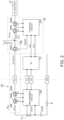
- FIG. 2 is a schematic block diagram illustrating the circuit layout example according to the present embodiment.
- the power supply circuit 33 includes the charging circuit 332 and FETs 334a, 334b, and 334c.
- the battery pack 34 includes the measurement circuit 342, FETs 344a and 344b, a fuse 346, and cells CL01 and CL02.
- a power line is electrically connected to the positive electrode of the cell CL01 from the AC adapter 37 via the FETs 334a, 334b, 334c, 344a, 344b, and the fuse 346.
- the cells CL01 and CL02 are connected in series.
- the negative electrode of the cell CL02 is grounded (GND) through a resistance element R. This can result in avoiding or reducing the damage to the cells CL0 and CL02 due to reverse connection of the cells CL01 and CL02, or an unexpected voltage application to the negative electrode.
- the FET (Field Effect Transistor) 334a prevents a reverse current flow from a branch point 336 to the AC adapter 37.
- the FET 334b adjusts the current from the AC adapter 37 to the branch point 336 under the control of the charging circuit 332.
- the FET 334c switches whether or not there is conduction between the branch point 336 and the battery pack 34 under the control of the charging circuit 332.
- the FET 344a controls the current discharged from the cells CL01 and CL02 under the control of the measurement circuit 342.
- the FET 344b controls the current charged to the cells CL01 and CL02 under the control of the measurement circuit 342.
- the source electrode (which may also be called the “S electrode” below), the drain electrode (which may also be called the “D electrode” below), and the gate electrode (which may also be called the “G electrode” below) of the FET 334a are electrically connected to the AC adapter 37, the D electrode of the FET 334b, and the charging circuit 332, respectively.
- the FET 334a can prevent a reverse current flow from the FET 334b to the AC adapter 37 by keeping the voltage applied to the G electrode from becoming significantly higher than 0 V.
- the S electrode, the D electrode, and the G electrode of the FET 334b are electrically connected to the branch point 336, the D electrode of the FET 334a, and the charging circuit 332, respectively.
- the current flowing from the AC adapter 37 can be increased.
- the S electrode, the D electrode, and the G electrode of the FET 334c are electrically connected to the battery pack 34, the branch point 336, and the charging circuit 332, respectively.
- the open/close control signal is a binary signal that can take two levels of potential. Between the two levels of potential, the lower level is called a low potential (L) and the higher level is called a high potential (H).
- the low potential is, for example, a potential within a predetermined range from 0 V.
- the high potential is a positive potential significantly higher than the low potential.
- the charging circuit 332 applies the open/close control signal having the high potential to the G electrode of the FET 334c, while when the battery pack 34 is not charged, the charging circuit 332 stops the application of the open/close control signal having the high potential to the G electrode of the FET 334c.
- the branch point 336 supplies, to the system, system power as part of the DC power supplied from the AC adapter 37, and supplies the remaining charging power to the battery pack 34 via the FET 334c.
- the total current value I total of the supplied DC power corresponds to the sum of a system current I sys as a current value of the system power and a charging current I bat as a current value of the charging power.
- the S electrode, the D electrode, and the G electrode of the FET 344a are electrically connected to the power supply circuit 33, the D electrode of the FET 344b, and the measurement circuit 342, respectively.
- the power current discharged from the cell CL01 can be increased.
- the S electrode, the D electrode, and the G electrode of the FET 344b are electrically connected to the fuse 346, the D electrode of the FET 344a, and the measurement circuit 342, respectively.
- the power current charged from the power supply circuit 33 to the cells CL01 and CL02 can be increased.
- the S electrode, the D electrode, and the G electrode of the FET 334b are electrically connected to the branch point 336, the D electrode of the FET 334a, and the charging circuit 332, respectively.
- the current flowing from the AC adapter 37 can be increased.
- the fuse 346 cuts off the current flowing therethrough. Thus, an excessive current flowing into or out of the cells CL01 and CL02 can be prevented.
- the charging circuit 332 and the measurement circuit 342 are connected to the EC 31 using signal lines, respectively.
- the signal lines include a data signal line (DAT) and a clock signal line (CLK).
- DAT data signal line
- CLK clock signal line
- the data signal line is used to transmit a control signal and other data.
- the clock signal line is used to transmit a clock signal.
- the charging circuit 332 and the measurement circuit 342 synchronize with the EC 31 using the clock signal input from the EC 31, respectively.
- As the signal line for example, a system management bus (SMB) is used.
- SMB system management bus
- the charged state information is input from the measurement circuit 342 to the charging circuit 332 via the EC 31.
- the charging circuit 332 controls charging to the battery pack 34 based on the charged state indicated by the charged state information.
- the charging circuit 332 realizes constant current (CC) charging and constant voltage (CV) charging as main charging methods.
- the CC charging means a charging mode for charging with a preset constant charging current value. According to the CC charging, since charging with a relatively large current is enabled, an electromotive force increases and the resistance decreases as the cell charge is accumulated in the battery pack 34.
- the CC charging may be performed at such a stage that the charging voltage V charge for charging the battery pack 34 does not reach a constant charging voltage value.
- the CV charging means a charging mode for charging with a preset constant charging voltage.
- the CV charging is started at the time when the charging voltage V charge has reached a predetermined charging voltage V charge,CV , and the charging voltage V charge is maintained at the constant value V charge,CV after that.
- the cell voltage V cell inside the battery pack 34 tends to be lower than the charging voltage V charge .
- the cell voltage V cell inside the battery pack 34 gets close to the charging voltage V charge and the charging current decreases. The full charge determination can be made during the CV charging.
- the charging circuit 332 makes the full charge determination.
- the charging circuit 332 stops charging the battery pack 34.
- a first taper voltage V tp,1 is preset in the charging circuit 332.
- a voltage design value lower by a predetermined minute margin voltage ⁇ V (for example, by 50 to 200 mV) than the charging voltage V charge,CV in the fully charged state can be used as the first taper voltage V tp,1 .
- the charging circuit 332 estimates the taper voltage when fully charged as a second taper voltage V tp,2 based on the cell voltage V cell of the battery pack 34 at the time.
- the power supply circuit 33 updates the predetermined taper voltage used for the full charge determination from the first taper voltage V tp,1 to the estimated second taper voltage V tp,2 .
- a predetermined reference charging time for example, 8 to 20 hours
- the power supply circuit 33 changes the predetermined taper voltage from the second taper voltage V tp,2 to the first taper voltage V tp,1 .
- the estimation method of the second taper voltage V tp,2 will be described later.
- the charging circuit 332 is, for example, a system charger IC.
- the measurement circuit 342 is a circuit for measuring the charged state to the cells CL01 and CL02.
- the measurement circuit 342 measures the potential at the positive electrode of the cell CL01 as the cell voltage V cell , and measures the current flowing from the power supply circuit 33 as the charging current I bat .
- the measurement circuit 342 outputs charged state information indicative of the measured cell voltage V cell and charging current I bat to the charging circuit 332 via the EC 31.
- the charging circuit 332 controls charging based on the charged state indicated by the charged state information input from the measurement circuit 342.
- the measurement circuit 342 adjusts the potentials applied to the respective G electrodes of the FET 344a and the FET 344b to control discharging from the cell CL01 and charging to the cell CL02, respectively.
- the measurement circuit 342 is, for example, a battery fuel gauge IC (Integrated Circuit).
- the EC 31 When no electric power is supplied from the AC adapter 37, the EC 31 notifies the measurement circuit 342 of the system current I sys to discharge a current corresponding to the system current I sys from the cells CL01 and CL02.
- a first example of the estimation method is a method for determining the cell voltage V cell when full charge is detected in off charge to be the second taper voltage V tp,2 .
- the charging circuit 332 can determine that the charging method is the system non-operating charge, that is, that charging is in a state where no electric power is supplied to the system.
- the cell voltage V cell is notified from the measurement circuit 342 to the charging circuit 332 via the EC 31.
- the charging circuit 332 makes the full charge determination using the newly determined second taper voltage V tp,2 instead of the first taper voltage V tp,1 .
- the charging current I bat decreases over time in a state of exceeding the taper current I tp . Therefore, the full charge determination is not made immediately. In on charge, the charging current I bat decreases and may be temporarily below the taper current I tp due to power consumption in the system.
- the state of the cells CL01 and CL02 is erroneously determined to be the fully charged state despite the fact that the cells CL01 and CL02 do not reach the fully charged state.
- the full charge determination is not made immediately.
- the second taper voltage V tp,2 detected at the off-charge time can be compared with the cell voltage V cell , the full charge determination can be made correctly. Further, individual differences can be resolved by adopting the actually detected cell voltage V cell as the second taper voltage V tp,2 .
- a second example of the estimation method is a method in which, when the charging mode is changed from CC charging to CV charging, a voltage dropped from the constant charging voltage V charge,CV due to a voltage drop V dp based on the circuit resistance in a path from the power supply circuit 33 to the cell CL01 and the predetermined taper current I tp is determined to be the second taper voltage V tp,2 .
- the charging mode is changed from CC charging to CV charging when the charging voltage V charge reaches the predetermined constant charging voltage V charge,CV related to CV charging.
- the EC 31 measures the voltage at the branch point 336 as the charging voltage V charge .
- the EC 31 When determining that the charging voltage V charge has reached the constant charging voltage V charge,CV , the EC 31 notifies the charging circuit 332 of a charging mode changing instruction from CC charging to CV charging.
- the charging circuit 332 changes the charging mode from CC charging to CV charging.
- the circuit resistance R cir in a path from the branch point 336 to the positive electrode of the cell CL01 is caused by the FETs 334c, 344a, 344b, and the fuse 346.
- the charging circuit 332 can determine the second taper voltage V tp,2 by subtracting, from the charging voltage V charge,CV , a voltage drop R cir ⁇ I tp due to the taper current I tp in the circuit resistance R cir .
- FIG. 5 is a flowchart illustrating charging control processing according to the present embodiment.
- the processing in FIG. 5 is executed during charging to the battery pack 34.
- Step S102 The charging circuit 332 monitors the cell voltage V cell notified from the measurement circuit 342 to determine whether or not the cell voltage V cell becomes the taper voltage V tp or more set at the time.
- the taper voltage V tp can be either one of the first taper voltage V tp,1 and the second taper voltage V tp,2 .
- step S104 the charging circuit 332 proceeds to a process in step S104.
- step S102 NO
- the charging circuit 332 repeats the process in step S102.
- Step S104 The charging circuit 332 determines whether or not the charging current I bat becomes the predetermined taper current I tp or less. When determining that the charging current I bat is the taper current I tp or less (step S104: YES), the charging circuit 332 proceeds to a process in step S106. When determining that the charging current I bat exceeds the taper current I tp (step S104: NO), the charging circuit 332 returns to the process in step S102.
- Step S106 The charging circuit 332 determines that the charged state of the battery pack 34 is the fully charged state, and stops charging to the battery pack 34. At this time, the charging circuit 332 stops the application of the open/close control signal having the high potential (H) to the G electrode of the FET 334c to cut off the charging power. After that, the processing in FIG. 5 is ended.
- Processing in FIG. 6 and FIG. 7 takes, as an example, a case where the first taper voltage V tp,1 is preset in the charging circuit 332 as the initial value of the taper voltage V tp .
- FIG. 6 is a flowchart illustrating a first example of taper voltage setting processing according to the present embodiment.
- Step S202 The charging circuit 332 determines whether or not the charging state at the time is off charge. For example, when the charging current I bat from the branch point 336 toward the battery pack 34 is a positive value significantly larger than 0 A and no system power is required by the system power request notified from the EC 31, the charging circuit 332 determines off charge, or otherwise, the charging circuit 332 can determine that the charging state is not off charge.
- step S202: YES the charging circuit 332 proceeds to a process in step S204.
- step S202: NO the charging circuit 332 repeats the process in step S202 without changing the taper voltage.
- Step S204 The charging circuit 332 makes the full charge determination using the first taper voltage V tp,1 and the preset taper current I tp ( FIG. 5 ).
- step S204: YES the procedure proceeds to a process in step S206.
- step S204: NO the charging circuit 332 returns to the process in step S202 without changing the taper voltage.
- Step S206 The measurement circuit 342 measures the cell voltage V cell and notifies the charging circuit 332 of the measured cell voltage V cell .
- Step S208 The charging circuit 332 determines the cell voltage V cell notified from the measurement circuit 342 to be the second taper voltage V tp,2 , and changes the taper voltage V tp used for the full charge determination from the first taper voltage V tp,1 to the second taper voltage V tp,2 .
- Step S210 The charging circuit 332 determines whether or not the charged state reaches the fully charged state within a certain period of time from the start of charging. When determining that the charged state does not reach the fully charged state even after the certain period of time has passed (step S210: NO), the charging circuit 332 changes the taper voltage V tp to the first taper voltage V tp,1 , and returns to the process in step S202. When determining that the charged state reaches the fully charged state (step S210: YES), the charging circuit 332 repeats the process in step S210 without changing the second taper voltage V tp,2 .
- FIG. 7 is a flowchart illustrating a second example of taper voltage setting processing according to the present embodiment.
- Step S302 The charging circuit 332 determines whether or not the charging state at the time is on charge. For example, when the charging current I bat from the branch point 336 toward the battery pack 34 is a positive value significantly larger than 0 A, the charging circuit 332 determines on charge, or otherwise, the charging circuit 332 can determine that the charging state is not on charge.
- step S302: YES the charging circuit 332 proceeds to a process in step S304.
- step S302: NO the charging circuit 332 repeats the process in step S302 without changing the first taper voltage V tp,1 .
- Step S304 The charging circuit 332 monitors whether or not the charging mode changing instruction is input from the EC 31 to determine whether or not the charging mode is changed from CC charging to CV charging.
- step S304: YES the charging circuit 332 proceeds to a process in step S306.
- step S304: NO the charging circuit 332 returns to the process in step S302 without changing the first taper voltage V tp,1 .
- Step S306 The charging circuit 332 calculates the circuit resistance R cir from a potential difference between the charging voltage V charge and the cell voltage V cell at the time, and the charging current I bat .
- the measurement circuit 342 measures the cell voltage V cell and notifies the charging circuit 332 of the measured cell voltage V cell .
- the charging circuit 332 measures the charging voltage V charge and the charging current I bat .
- Step S308 The charging circuit 332 calculates the second taper voltage V tp,2 by subtracting, from the charging voltage V charge , the voltage drop R cir ⁇ I tp by the taper current I tp based on the circuit resistance R cir , and changes the taper voltage V tp used for the full charge determination from the first taper voltage V tp,1 to the second taper voltage V tp,2 .
- Step S310 The charging circuit 332 determines whether or not the charged state reaches the fully charged state within the certain period of time. When determining that the charged state does not reach the fully charged state even after the certain period of time has passed (step S310: NO), the charging circuit 332 changes the taper voltage V tp to the first taper voltage Vt p,1 , and returns to the process in step S302. When determining that the charged state reaches the fully charged state (step S310: YES), the charging circuit 332 repeats the process in step S310 without changing the second taper voltage V tp,2 .
- the power supply circuit 33 supplies, to the system, system power required for the system out of DC power supplied from the power supply, and charges a battery (for example, the battery pack 34) with charging power as the remaining power, and when the cell voltage of the battery is a predetermined detection voltage (that is, the taper voltage) or more and a charging current of the charging power becomes a predetermined detection current (that is, the taper current) or less, the power supply circuit 33 determines that the battery charged state is fully charged.
- a predetermined detection voltage that is, the taper voltage
- a charging current of the charging power becomes a predetermined detection current (that is, the taper current) or less
- the power supply circuit 33 estimates, as a second detection voltage (for example, the second taper voltage), a cell voltage at the time when determining that the charged state is full charge based on the cell voltage obtained under a specific charging condition to the battery, and updates the predetermined detection voltage from a predetermined first detection voltage (for example, the first taper voltage) to the second detection voltage.
- a second detection voltage for example, the second taper voltage
- the cell voltage when fully charged which is estimated based on the cell voltage of the battery that meets the specific charging condition, is determined to be the detection voltage used for determining that the battery charged state has reached full charge. Therefore, even when the charging current temporarily drops due to power consumption in the system, if the measured cell voltage does not reach the cell voltage when fully charged, erroneous determination that the battery charged state is full charge can be avoided. Therefore, charging to the battery can continue more securely until the battery charged state reaches the fully charged state. Further, since the second detection voltage is estimated from the cell voltage based on the actually detected charging condition, a fully charged state adapted to individual electrical characteristics can be detected regardless of individual differences.
- the cell voltage at the time when determining that the charged state is full charge may be determined to be the second detection voltage.
- the fully charged state is detected by avoiding a temporary charging current due to power consumption in the system, and the cell voltage at the time is used as the second detection voltage for determining the fully charged state. Therefore, even when the charging current temporarily drops, if the cell voltage does not exceed the second detection voltage, erroneous detection of the fully charged state can be avoided.
- the power supply circuit may measure a circuit resistance value from the power supply circuit to the battery based on the charging voltage to the battery, the cell voltage, and the charging current, and determine a voltage dropped from the charging voltage due to the circuit resistance value and the detection current to be the second detection voltage.
- the cell voltage is estimated as the second detection voltage based on the circuit resistance value determined by the voltage drop from the charging voltage to the cell voltage when the charging mode is changed, and the charging current. Therefore, even when the charging current temporarily drops, if the cell voltage does not exceed the second detection voltage, erroneous detection of the fully charged state can be avoided.
- the power supply circuit may change the predetermined detection voltage to the first detection voltage.
- the power supply circuit 33 may also include the battery pack 34 in a manner to be integrally constructed as a single power supply circuit 33.
- the number of cells included in the battery pack 34 is not limited to two, which may be one, or three or more. When the battery pack 34 includes two or more cells, some or all of these cells may also be connected in parallel.
Landscapes
- Engineering & Computer Science (AREA)
- Power Engineering (AREA)
- Manufacturing & Machinery (AREA)
- Chemical & Material Sciences (AREA)
- Chemical Kinetics & Catalysis (AREA)
- Electrochemistry (AREA)
- General Chemical & Material Sciences (AREA)
- Charge And Discharge Circuits For Batteries Or The Like (AREA)
- Power Sources (AREA)
Abstract
Description
- The present invention relates to a power supply circuit, an electronic apparatus, and a control method related, for example, to battery charging.
- Battery packs may be equipped in information apparatuses, such as PCs (Personal Computers), tablet terminals, smartphones, and other various electronic apparatuses. An electronic apparatus is operable by consuming electric power charged in a battery pack even when no electric power is supplied from outside. In the battery pack, a battery (secondary battery) is charged from an AC (Alternating Current) adapter under the control of a power supply circuit, which is a system charging IC (Integrated Circuit), for example.
- For example, a charging method disclosed in
Japanese Unexamined Patent Application Publication No. H04-183232 - As charging methods from a system to a battery, there are system non-operating charge (also called system off charge or off charge) and system operating charge (also called system operation charge or on charge). The system non-operating charge is a method for charging only the battery without supplying electric power to the system.
The system operating charge is a method for charging the battery as well while supplying electric power to the system. In the system non-operating charge, almost all of supply current Itotal supplied from the AC adapter is charged to the battery. When conditions that a cell voltage generated in the battery becomes a predetermined detection voltage (also called a taper voltage) or more, and a charging current becomes a predetermined detection current (also called a taper current) or less are met, a controller determines that the charged state of the battery has reached a fully charged state, and charging is finished. - However, in the system operating charge, a required current out of the supplied charging current Itotal is supplied to the system as a system current Isys. A residual current Itotal-Isys after removing, from the supply current Itotal, the system current Isys supplied to the system is supplied to the battery. Therefore, the supplied current may not meet the battery requirements. Especially, when an AC adapter with low-rated power is used, a decrease in charging power to be charged to the battery may become noticeable. Under such circumstances, even when the conditions that the cell voltage becomes the taper voltage or more and the charging current becomes the taper current or less are met, the capacity of electric charge stored in the battery may become smaller than the capacity in the fully charged state (full charge capacity) originally expected.
- As a cause, it is considered that a voltage lower by a given margin than the rated value of a system voltage supplied from the system is set as the taper voltage. When a full charge determination is made by relying on the fixed taper voltage due to the fact that the charging current becomes the taper current or less, the charge capacity stored in the battery may be lower than the full charge capacity. The taper voltage depends on circuit resistance values of the battery and the system, but these circuit resistance values vary individually. In order to ensure safety or stability, a larger margin than necessary tends to be set on each individual equipment by taking individual differences into account at the design stage.
- The present application has been made to solve the above problem, and a power supply circuit according to the first aspect of the present application supplies, to a system, system power required for the system out of DC power supplied from a power supply, and charges a battery with charging power as the remaining power, and when a cell voltage of the battery is a predetermined detection voltage or more and a charging current of the charging power becomes a predetermined detection current or less, the power supply circuit determines that the charged state of the battery is fully charged, wherein the cell voltage at the time when it is determined that the charged state is fully charged based on the cell voltage obtained in a specific charging state to the battery is estimated as a second detection voltage, and the predetermined detection voltage is updated from a predetermined first detection voltage to the second detection voltage.
- The above power supply circuit may be such that, when charging the battery with the charging power without supplying the system power to the system, the cell voltage at the time when determining that the charged state is fully charged is determined to be the second detection voltage.
- The above power supply circuit may also be such that, when a charging method for the battery is changed from a first charging mode for charging with a constant charging current to a second charging mode for charging with a constant charging voltage, a circuit resistance value from the power supply circuit to the battery is measured based on a charging voltage to the battery, the cell voltage, and the charging current, and a voltage dropped from the charging voltage due to the circuit resistance value and the detection current is determined to be the second detection voltage.
- The above power supply circuit may further be such that, when determining that the charged state is not fully charged even after the charging time to the battery exceeds a predetermined reference charging time, the predetermined detection voltage is changed to the first detection voltage.
- Further, the above power supply circuit may include the battery.
- An electronic apparatus according to the second aspect of the present application may include the above power supply circuit.
- A control method according to the third aspect of the present application is a control method for a power supply circuit which supplies, to a system, system power required for the system out of DC power supplied from a power supply, and charges a battery with charging power as the remaining power, and when a cell voltage of the battery is a predetermined detection voltage or more and a charging current of the charging power becomes a predetermined detection current or less, the power supply circuit determines that the battery charged state is fully charged, wherein the power supply circuit estimates, as a second detection voltage, the cell voltage at the time when determining that the charged state is fully charged based on the cell voltage obtained in a specific charging state to the battery, and updates the predetermined detection voltage from a predetermined first detection voltage to the second detection voltage.
- The embodiment according to the above-described aspects of the present application can finish charging more accurately in the fully charged state even when electric power is consumed in the system.
-
-
FIG. 1 is a schematic block diagram illustrating a hardware configuration example of an electronic apparatus according to an embodiment. -
FIG. 2 is a schematic block diagram illustrating a circuit layout example according to the present embodiment. -
FIG. 3 is a graph illustrating a first example of the time lapse of a cell voltage and a charging current upon charging. -
FIG. 4 is a graph illustrating a second example of the time lapse of the cell voltage and the charging current upon charging. -
FIG. 5 is a flowchart illustrating charging control processing according to the present embodiment. -
FIG. 6 is a flowchart illustrating a first example of detection voltage setting processing according to the present embodiment. -
FIG. 7 is a flowchart illustrating a second example of detection voltage setting processing according to the present embodiment. - An embodiment of the present application will be described with reference to the accompanying drawings. First, the overview of an
electronic apparatus 1 according to the embodiment of the present application will be described. Theelectronic apparatus 1 includes apower supply circuit 33. Thepower supply circuit 33 supplies, to a system, system power required for the system out of DC power supplied from a DC power supply, and charges a battery with the remaining charging power. When a cell voltage of the battery is a predetermined taper voltage or more and a charging current of the charging power becomes a predetermined detection current or less, thepower supply circuit 33 determines that the battery charged state is fully charged. In the present embodiment, the taper voltage is set to a variable value rather than a fixed value. Here, when battery charging conditions meet specific charging conditions, thepower supply circuit 33 estimates, as a second taper voltage, the taper voltage when fully charged based on the cell voltage. Thepower supply circuit 33 updates the predetermined taper voltage from a predetermined first taper voltage to the second taper voltage. - The
electronic apparatus 1 according to the present embodiment can be an electronic apparatus typically having a convenient size and weight to carry and consuming electric power stored in the battery. Theelectronic apparatus 1 may be any form of information apparatus such as a PC, a smartphone, or a tablet terminal. Theelectronic apparatus 1 may also be an apparatus, such as a measuring instrument or a monitoring device, installed in an environment difficult to supply electric power constantly from a DC power supply. The following description is mainly made when theelectronic apparatus 1 is a personal computer (PC). Further, the "system" in the present application may indicate a device, that is, a load, that consumes electric power supplied from thepower supply circuit 33 in theelectronic apparatus 1. When theelectronic apparatus 1 is an information apparatus, power consumption in the computer system (also called a host system) usually accounts for most of processing of theelectronic apparatus 1. -
FIG. 1 is a schematic block diagram illustrating a hardware configuration example of theelectronic apparatus 1 according to the present embodiment. Theelectronic apparatus 1 includes aCPU 11, amain memory 12, avideo subsystem 13, adisplay 14, a PCH (Platform Controller Hub) 21, a BIOS (Basic Input Output System)memory 22, anauxiliary storage device 23, a WLAN (Wireless Local Area Network)card 25, a USB (Universal Serial Bus)connector 26, an EC (Embedded Controller) 31, aninput unit 32, thepower supply circuit 33, abattery pack 34, and apower button 38. - The
CPU 11 is a processor that forms the core of a system device included in theelectronic apparatus 1. TheCPU 11 is a processor that executes various kinds of arithmetic processing directed by commands written in software (programs). For example, theCPU 11 executes processing instructed by various kinds of software such as an OS (Operating System), a BIOS, and application programs (called "apps" or "applications" in the present application). Note that the fact that the processing directed by commands written in software is executed may also be referred to as that "software is executed." - The
main memory 12 is a writable memory used as reading areas of execution programs of the processor or working areas to which processing data of the execution programs are written. Themain memory 12 is composed, for example, of plural DRAM (Dynamic Random Access Memory) chips. The execution programs include the OS, various drivers for operating hardware such as peripheral devices, various services/utilities, apps, and the like. - The
CPU 11 and themain memory 12 function as a computer system that forms the core of theelectronic apparatus 1, that is, a system device that forms a host system. The computer system of theelectronic apparatus 1 is configured to include system devices as hardware, the OS, and software such as Schedule Task and the like. - The
video subsystem 13 executes image processing under the control of theCPU 11. Thevideo subsystem 13 includes a video controller and a video memory (not illustrated). The video controller performs image processing according to drawing commands input from theCPU 11 to generate drawing information and to write the generated drawing information to the video memory (not illustrated). The video controller reads the drawing information from the video memory, and outputs, to thedisplay 14, display data indicative of the read drawing information (image processing). - On the other hand, the
CPU 11 executes a graphics driver on the OS to control the operation of thevideo subsystem 13. TheCPU 11 outputs, to thevideo subsystem 13, the drawing commands by the OS, the apps, or other programs to realize the image processing. - The
display 14 displays a display screen based on the display data output from theCPU 11. Thedisplay 14 may be any one of a liquid crystal display (LCD), an OLED (Organic Light Emitting Diode) display, and the like. - The
PCH 21 includes one or more controllers to enable connection to plural devices so that various data can be input and output. For example, thePCH 21 is any one or a combination of bus controllers, such as USB, serial ATA (Advanced Technology Attachment), an SPI (Serial Peripheral Interface) bus, a PCI (Peripheral Component Interconnect) bus, a PCI-Express bus, and an LPC (Low Pin Count) bus. The plural devices as connection destinations correspond, for example, to theBIOS memory 22, theauxiliary storage device 23, theWLAN card 25, theUSB connector 26, and theEC 31. - The
BIOS memory 22 is configured as an electrically rewritable non-volatile memory. Such a non-volatile memory corresponds, for example, to an EEPROM (Electrically Erasable Programmable Read Only Memory), a flash ROM (Read Only Memory), or the like. TheBIOS memory 22 stores a BIOS, firmware for controlling the operation of theEC 31 and other devices, and the like. The BIOS is firmware for basic input and output of the system devices. In the present application, firmware defined according to the specifications stipulated in the UEFI (Unified Extensible Firmware Interface) can be included in the BIOS concept. - The
auxiliary storage device 23 sustainably stores various data. Data to be stored include various programs executable by theCPU 11 and other devices, parameters, data used in various processing, and data acquired by the various processing. For example, theauxiliary storage device 23 may be either one of an HDD (Hard Disk Drive) and an SSD (Solid State Drive). Theauxiliary storage device 23 is configured to include various non-volatile memories. As a non-volatile memory, for example, a flash memory is used. The various programs can include, for example, any one or a combination of the OS, drivers, firmware, apps, and the like. - The
WLAN card 25 is connected to a wireless LAN or any other network via the wireless LAN so that various data can be transmitted and received with devices as connection destinations. - The
USB connector 26 is a connector for connecting various peripheral devices using USB. - The
EC 31 is a one-chip microcomputer that monitors and controls the status of various devices (peripheral devices, sensors, and the like) regardless of the operating state of the host system that forms the core of theelectronic apparatus 1. TheEC 31 includes a ROM, multichannel A/D (Analog-to-Digital) input terminal and D/A (Digital-to-Analog) output terminal, a timer, and digital input/output terminals (not illustrated) in addition to a CPU separate from theCPU 11 and a RAM separate from themain memory 12. Theinput unit 32, thepower supply circuit 33, and the like are connected to the digital input/output terminals of theEC 31 so that theEC 31 can control the operation of these devices. - The
EC 31 monitors the operating state of each of the devices that construct theelectronic apparatus 1, and determines electric energy required for the operation to exceed the power consumption of each device (which may also be called "device power" in the present application). The total of device power corresponds to system power. The devices to be monitored include system devices of theelectronic apparatus 1, mainly including theCPU 11. TheEC 31 outputs, to thepower supply circuit 33, a system power request indicative of the device power for each device. As will be described later, electric power corresponding to the device power is supplied from thepower supply circuit 33 to each of the devices that construct the system. - The
input unit 32 includes input devices that detect user operations and output, to theEC 31, operation signals according to the detected operations. For example, the input devices included in theinput unit 32 correspond to a keyboard, a touch pad, and the like. A touch sensor that constructs part of theinput unit 32 may be configured as a touch panel which overlaps with thedisplay 14 that constructs a display unit. - DC power is supplied from an AC (Alternating Current)
adapter 37 to thepower supply circuit 33. Under the control of theEC 31, thepower supply circuit 33 supplies, to the system, system power required for the system out of the supplied DC power. Thepower supply circuit 33 supplies, to each device, electric power corresponding to the device power directed by the system power request for the device notified from theEC 31. Thepower supply circuit 33 supplies electric power corresponding to the system power as the entire system of theelectronic apparatus 1. Thepower supply circuit 33 charges thebattery pack 34 with the remaining power as charging power after removing the system power out of the supplied DC power. - The
power supply circuit 33 includes a charging circuit 332 (FIG. 2 ) and a converter (not illustrated).
The chargingcircuit 332 charges thebattery pack 34 with the charging power depending on the charged state in thebattery pack 34. When the cell voltage of thebattery pack 34 is a predetermined taper voltage or more and the charging current of the charging power becomes a predetermined taper current or less, the chargingcircuit 332 determines that the charged state of thebattery pack 34 is fully charged. In the present application, the determination of whether or not the charged state has reached a fully charged state or the determination result may also be called the "full charge determination." When the full charge determination is made, the chargingcircuit 332 stops charging to thebattery pack 34. - The converter converts the voltage of electric power supplied from the
AC adapter 37 to the own apparatus into a voltage required for each device. The converter supplies electric power with the converted voltage to the device for which the electric power with the converted voltage is required. - The
battery pack 34 includes one or more batteries (also called secondary batteries, cells, or the like), and a measurement circuit 342 (not illustrated). Themeasurement circuit 342 measures a charging voltage and a charging current as the battery charged state, and notifies thepower supply circuit 33 of charged state information indicative of the measured charging voltage and charging current. In the battery (or the batteries), charging power supplied from thepower supply circuit 33 is stored. - The
AC adapter 37 converts AC power supplied from an external power supply into DC power with a constant voltage, and supplies the converted power to thepower supply circuit 33. TheAC adapter 37 is connected to thepower supply circuit 33 in a manner to enable input/output of control signals. TheAC adapter 37 includes an attachment attachable to and detachable from the chassis of theelectronic apparatus 1 including thepower supply circuit 33. TheAC adapter 37 may also be connected to theUSB connector 26 in a physically attachable/detachable manner. - The
power button 38 controls whether or not there is the supply of electric power to the entire electronic apparatus 1 (Power ON/OFF) each time a press operation is accepted. Thepower button 38 outputs, to theEC 31, a press signal indicative of a press. When the press signal is input from thepower button 38 while theelectronic apparatus 1 is in a power cut-off state (in a state without power supply), theEC 31 causes thepower supply circuit 33 to start the supply of electric power to each device of the electronic apparatus 1 (power on). When the press signal is input from thepower button 38 while theelectronic apparatus 1 is being energized (with power supply), theEC 31 causes thepower supply circuit 33 to stop the supply of electric power to each device of the electronic apparatus 1 (power cut-off). - Next, a circuit layout example according to the present embodiment will be described.
FIG. 2 is a schematic block diagram illustrating the circuit layout example according to the present embodiment. - The
power supply circuit 33 includes the chargingcircuit 332 andFETs battery pack 34 includes themeasurement circuit 342,FETs fuse 346, and cells CL01 and CL02. - A power line is electrically connected to the positive electrode of the cell CL01 from the
AC adapter 37 via theFETs fuse 346. The cells CL01 and CL02 are connected in series. The negative electrode of the cell CL02 is grounded (GND) through a resistance element R. This can result in avoiding or reducing the damage to the cells CL0 and CL02 due to reverse connection of the cells CL01 and CL02, or an unexpected voltage application to the negative electrode. - The FET (Field Effect Transistor) 334a prevents a reverse current flow from a
branch point 336 to theAC adapter 37. TheFET 334b adjusts the current from theAC adapter 37 to thebranch point 336 under the control of the chargingcircuit 332. TheFET 334c switches whether or not there is conduction between thebranch point 336 and thebattery pack 34 under the control of the chargingcircuit 332. TheFET 344a controls the current discharged from the cells CL01 and CL02 under the control of themeasurement circuit 342. TheFET 344b controls the current charged to the cells CL01 and CL02 under the control of themeasurement circuit 342. - The source electrode (which may also be called the "S electrode" below), the drain electrode (which may also be called the "D electrode" below), and the gate electrode (which may also be called the "G electrode" below) of the
FET 334a are electrically connected to theAC adapter 37, the D electrode of theFET 334b, and the chargingcircuit 332, respectively. TheFET 334a can prevent a reverse current flow from theFET 334b to theAC adapter 37 by keeping the voltage applied to the G electrode from becoming significantly higher than 0 V. - The S electrode, the D electrode, and the G electrode of the
FET 334b are electrically connected to thebranch point 336, the D electrode of theFET 334a, and the chargingcircuit 332, respectively. By increasing the positive potential applied to the G electrode of theFET 334b, the current flowing from theAC adapter 37 can be increased. - The S electrode, the D electrode, and the G electrode of the
FET 334c are electrically connected to thebattery pack 34, thebranch point 336, and the chargingcircuit 332, respectively. By applying an open/close control signal from the chargingcircuit 332 to the G electrode of theFET 334c, it is controlled whether or not there is conduction from thebranch point 336 to the battery pack 34 (ON/OFF). The open/close control signal is a binary signal that can take two levels of potential. Between the two levels of potential, the lower level is called a low potential (L) and the higher level is called a high potential (H). The low potential is, for example, a potential within a predetermined range from 0 V. The high potential is a positive potential significantly higher than the low potential. When thebattery pack 34 is charged, the chargingcircuit 332 applies the open/close control signal having the high potential to the G electrode of theFET 334c, while when thebattery pack 34 is not charged, the chargingcircuit 332 stops the application of the open/close control signal having the high potential to the G electrode of theFET 334c. - The
branch point 336 supplies, to the system, system power as part of the DC power supplied from theAC adapter 37, and supplies the remaining charging power to thebattery pack 34 via theFET 334c. The total current value Itotal of the supplied DC power corresponds to the sum of a system current Isys as a current value of the system power and a charging current Ibat as a current value of the charging power. - The S electrode, the D electrode, and the G electrode of the
FET 344a are electrically connected to thepower supply circuit 33, the D electrode of theFET 344b, and themeasurement circuit 342, respectively. By increasing the positive potential applied to the G electrode of theFET 344a, the power current discharged from the cell CL01 can be increased. - The S electrode, the D electrode, and the G electrode of the
FET 344b are electrically connected to thefuse 346, the D electrode of theFET 344a, and themeasurement circuit 342, respectively. By increasing the positive potential applied to the G electrode of theFET 344b, the power current charged from thepower supply circuit 33 to the cells CL01 and CL02 can be increased. - The S electrode, the D electrode, and the G electrode of the
FET 334b are electrically connected to thebranch point 336, the D electrode of theFET 334a, and the chargingcircuit 332, respectively. By increasing the positive potential applied to the G electrode of theFET 334b, the current flowing from theAC adapter 37 can be increased. - When a current exceeding a predetermined limit value is detected, the
fuse 346 cuts off the current flowing therethrough. Thus, an excessive current flowing into or out of the cells CL01 and CL02 can be prevented. - The charging
circuit 332 and themeasurement circuit 342 are connected to theEC 31 using signal lines, respectively. The signal lines include a data signal line (DAT) and a clock signal line (CLK). The data signal line is used to transmit a control signal and other data. The clock signal line is used to transmit a clock signal. The chargingcircuit 332 and themeasurement circuit 342 synchronize with theEC 31 using the clock signal input from theEC 31, respectively. As the signal line, for example, a system management bus (SMB) is used. - The charged state information is input from the
measurement circuit 342 to the chargingcircuit 332 via theEC 31. The chargingcircuit 332 controls charging to thebattery pack 34 based on the charged state indicated by the charged state information. The chargingcircuit 332 realizes constant current (CC) charging and constant voltage (CV) charging as main charging methods. The CC charging means a charging mode for charging with a preset constant charging current value. According to the CC charging, since charging with a relatively large current is enabled, an electromotive force increases and the resistance decreases as the cell charge is accumulated in thebattery pack 34. The CC charging may be performed at such a stage that the charging voltage Vcharge for charging thebattery pack 34 does not reach a constant charging voltage value. - The CV charging means a charging mode for charging with a preset constant charging voltage. The CV charging is started at the time when the charging voltage Vcharge has reached a predetermined charging voltage Vcharge,CV, and the charging voltage Vcharge is maintained at the constant value Vcharge,CV after that. At this stage, the cell voltage Vcell inside the
battery pack 34 tends to be lower than the charging voltage Vcharge. According to the CV charging, the cell voltage Vcell inside thebattery pack 34 gets close to the charging voltage Vcharge and the charging current decreases. The full charge determination can be made during the CV charging. - When the cell voltage Vcell of the
battery pack 34 is the predetermined taper voltage or more and the charging current Ibat of the charging power becomes a predetermined taper current Itp or less, the chargingcircuit 332 makes the full charge determination. When making the full charge determination, the chargingcircuit 332 stops charging thebattery pack 34. As an initial value of the predetermined taper voltage, a first taper voltage Vtp,1 is preset in thecharging circuit 332. In the example ofFIG. 4 , for example, a voltage design value lower by a predetermined minute margin voltage ΔV (for example, by 50 to 200 mV) than the charging voltage Vcharge,CV in the fully charged state can be used as the first taper voltage Vtp,1. - In the case where the charging conditions to the
battery pack 34 meet the specific charging conditions, the chargingcircuit 332 estimates the taper voltage when fully charged as a second taper voltage Vtp,2 based on the cell voltage Vcell of thebattery pack 34 at the time. Thepower supply circuit 33 updates the predetermined taper voltage used for the full charge determination from the first taper voltage Vtp,1 to the estimated second taper voltage Vtp,2. When the charged state of thebattery pack 34 is not fully charged even after the total charging time of thebattery pack 34 exceeds a predetermined reference charging time (for example, 8 to 20 hours), thepower supply circuit 33 changes the predetermined taper voltage from the second taper voltage Vtp,2 to the first taper voltage Vtp,1. The estimation method of the second taper voltage Vtp,2 will be described later. The chargingcircuit 332 is, for example, a system charger IC. - The
measurement circuit 342 is a circuit for measuring the charged state to the cells CL01 and CL02.
Themeasurement circuit 342 measures the potential at the positive electrode of the cell CL01 as the cell voltage Vcell, and measures the current flowing from thepower supply circuit 33 as the charging current Ibat. Themeasurement circuit 342 outputs charged state information indicative of the measured cell voltage Vcell and charging current Ibat to the chargingcircuit 332 via theEC 31. The chargingcircuit 332 controls charging based on the charged state indicated by the charged state information input from themeasurement circuit 342. - The
measurement circuit 342 adjusts the potentials applied to the respective G electrodes of theFET 344a and theFET 344b to control discharging from the cell CL01 and charging to the cell CL02, respectively. Themeasurement circuit 342 is, for example, a battery fuel gauge IC (Integrated Circuit). When no electric power is supplied from theAC adapter 37, theEC 31 notifies themeasurement circuit 342 of the system current Isys to discharge a current corresponding to the system current Isys from the cells CL01 and CL02. - Next, the estimation method of the second taper voltage Vtp,2 will be described. A first example of the estimation method is a method for determining the cell voltage Vcell when full charge is detected in off charge to be the second taper voltage Vtp,2. On the ground that the system power is zero or that the system power is unnecessary by the system power request notified from the
EC 31, the chargingcircuit 332 can determine that the charging method is the system non-operating charge, that is, that charging is in a state where no electric power is supplied to the system. The cell voltage Vcell is notified from themeasurement circuit 342 to the chargingcircuit 332 via theEC 31. The chargingcircuit 332 makes the full charge determination using the newly determined second taper voltage Vtp,2 instead of the first taper voltage Vtp,1. - In the example of
FIG. 3 , in off charge at a stage where the battery does not reach the fully charged state even after the cell voltage Vcell exceeds the first taper voltage Vtp,1, the charging current Ibat decreases over time in a state of exceeding the taper current Itp. Therefore, the full charge determination is not made immediately. In on charge, the charging current Ibat decreases and may be temporarily below the taper current Itp due to power consumption in the system. When the first taper voltage Vtp,1 is used in the full charge determination, the state of the cells CL01 and CL02 is erroneously determined to be the fully charged state despite the fact that the cells CL01 and CL02 do not reach the fully charged state. - However, by using the second taper voltage Vtp,2 as the taper voltage, since the cell voltage Vcell does not reach the second taper voltage Vtp,2 even when the charging current Ibat is temporarily below the taper current Itp, the full charge determination is not made immediately. Thus, since the second taper voltage Vtp,2 detected at the off-charge time can be compared with the cell voltage Vcell, the full charge determination can be made correctly. Further, individual differences can be resolved by adopting the actually detected cell voltage Vcell as the second taper voltage Vtp,2.
- A second example of the estimation method is a method in which, when the charging mode is changed from CC charging to CV charging, a voltage dropped from the constant charging voltage Vcharge,CV due to a voltage drop Vdp based on the circuit resistance in a path from the
power supply circuit 33 to the cell CL01 and the predetermined taper current Itp is determined to be the second taper voltage Vtp,2. In the example ofFIG. 4 , the charging mode is changed from CC charging to CV charging when the charging voltage Vcharge reaches the predetermined constant charging voltage Vcharge,CV related to CV charging. TheEC 31 measures the voltage at thebranch point 336 as the charging voltage Vcharge. When determining that the charging voltage Vcharge has reached the constant charging voltage Vcharge,CV, theEC 31 notifies the chargingcircuit 332 of a charging mode changing instruction from CC charging to CV charging. When the charging mode changing instruction is input from theEC 31, the chargingcircuit 332 changes the charging mode from CC charging to CV charging. The chargingcircuit 332 can calculate a circuit resistance Rcir by dividing the voltage drop Vdp (= Vcharge,CV - Vcell) from the charging voltage Vcharge,CV to the cell voltage Vcell at this time by the charging current Ibat. In the example ofFIG. 2 , the circuit resistance Rcir in a path from thebranch point 336 to the positive electrode of the cell CL01 is caused by theFETs fuse 346. The chargingcircuit 332 can determine the second taper voltage Vtp,2 by subtracting, from the charging voltage Vcharge,CV, a voltage drop Rcir×Itp due to the taper current Itp in the circuit resistance Rcir. - Next, an example of charging control processing according to the present embodiment will be described.
-
FIG. 5 is a flowchart illustrating charging control processing according to the present embodiment. - The processing in
FIG. 5 is executed during charging to thebattery pack 34. - (Step S102) The
charging circuit 332 monitors the cell voltage Vcell notified from themeasurement circuit 342 to determine whether or not the cell voltage Vcell becomes the taper voltage Vtp or more set at the time. In the present embodiment, the taper voltage Vtp can be either one of the first taper voltage Vtp,1 and the second taper voltage Vtp,2. When determining that the cell voltage Vcell is the taper voltage Vtp or more (step S102: YES), the chargingcircuit 332 proceeds to a process in step S104. When determining that the cell voltage Vcell is less than the taper voltage Vtp (step S102: NO), the chargingcircuit 332 repeats the process in step S102. - (Step S104) The
charging circuit 332 determines whether or not the charging current Ibat becomes the predetermined taper current Itp or less. When determining that the charging current Ibat is the taper current Itp or less (step S104: YES), the chargingcircuit 332 proceeds to a process in step S106. When determining that the charging current Ibat exceeds the taper current Itp (step S104: NO), the chargingcircuit 332 returns to the process in step S102. - (Step S106) The
charging circuit 332 determines that the charged state of thebattery pack 34 is the fully charged state, and stops charging to thebattery pack 34. At this time, the chargingcircuit 332 stops the application of the open/close control signal having the high potential (H) to the G electrode of theFET 334c to cut off the charging power. After that, the processing inFIG. 5 is ended. - Next, examples of taper voltage setting processing according to the present embodiment will be described. Processing in
FIG. 6 andFIG. 7 takes, as an example, a case where the first taper voltage Vtp,1 is preset in thecharging circuit 332 as the initial value of the taper voltage Vtp. -
FIG. 6 is a flowchart illustrating a first example of taper voltage setting processing according to the present embodiment. - (Step S202) The
charging circuit 332 determines whether or not the charging state at the time is off charge. For example, when the charging current Ibat from thebranch point 336 toward thebattery pack 34 is a positive value significantly larger than 0 A and no system power is required by the system power request notified from theEC 31, the chargingcircuit 332 determines off charge, or otherwise, the chargingcircuit 332 can determine that the charging state is not off charge. When determining off charge (step S202: YES), the chargingcircuit 332 proceeds to a process in step S204. When determining that the charging state is not off charge (step S202: NO), the chargingcircuit 332 repeats the process in step S202 without changing the taper voltage. - (Step S204) The
charging circuit 332 makes the full charge determination using the first taper voltage Vtp,1 and the preset taper current Itp (FIG. 5 ). When determining that the charged state of thebattery pack 34 is the fully charged state (step S204: YES), the procedure proceeds to a process in step S206. When determining that the charged state does not reach the fully charged state (step S204: NO), the chargingcircuit 332 returns to the process in step S202 without changing the taper voltage. - (Step S206) The
measurement circuit 342 measures the cell voltage Vcell and notifies the chargingcircuit 332 of the measured cell voltage Vcell. - (Step S208) The
charging circuit 332 determines the cell voltage Vcell notified from themeasurement circuit 342 to be the second taper voltage Vtp,2, and changes the taper voltage Vtp used for the full charge determination from the first taper voltage Vtp,1 to the second taper voltage Vtp,2. - (Step S210) The
charging circuit 332 determines whether or not the charged state reaches the fully charged state within a certain period of time from the start of charging. When determining that the charged state does not reach the fully charged state even after the certain period of time has passed (step S210: NO), the chargingcircuit 332 changes the taper voltage Vtp to the first taper voltage Vtp,1, and returns to the process in step S202.
When determining that the charged state reaches the fully charged state (step S210: YES), the chargingcircuit 332 repeats the process in step S210 without changing the second taper voltage Vtp,2. -
FIG. 7 is a flowchart illustrating a second example of taper voltage setting processing according to the present embodiment. - (Step S302) The
charging circuit 332 determines whether or not the charging state at the time is on charge. For example, when the charging current Ibat from thebranch point 336 toward thebattery pack 34 is a positive value significantly larger than 0 A, the chargingcircuit 332 determines on charge, or otherwise, the chargingcircuit 332 can determine that the charging state is not on charge. When determining on charge (step S302: YES), the chargingcircuit 332 proceeds to a process in step S304. When determining that the charging state is not on charge (step S302: NO), the chargingcircuit 332 repeats the process in step S302 without changing the first taper voltage Vtp,1. - (Step S304) The
charging circuit 332 monitors whether or not the charging mode changing instruction is input from theEC 31 to determine whether or not the charging mode is changed from CC charging to CV charging. When determining that the charging mode is changed to the CV charging (step S304: YES), the chargingcircuit 332 proceeds to a process in step S306. When determining that the charging mode is not changed to CV charging (step S304: NO), the chargingcircuit 332 returns to the process in step S302 without changing the first taper voltage Vtp,1. - (Step S306) The
charging circuit 332 calculates the circuit resistance Rcir from a potential difference between the charging voltage Vcharge and the cell voltage Vcell at the time, and the charging current Ibat. Here, themeasurement circuit 342 measures the cell voltage Vcell and notifies the chargingcircuit 332 of the measured cell voltage Vcell.
The chargingcircuit 332 measures the charging voltage Vcharge and the charging current Ibat. - (Step S308) The
charging circuit 332 calculates the second taper voltage Vtp,2 by subtracting, from the charging voltage Vcharge, the voltage drop Rcir×Itp by the taper current Itp based on the circuit resistance Rcir, and changes the taper voltage Vtp used for the full charge determination from the first taper voltage Vtp,1 to the second taper voltage Vtp,2. - (Step S310) The
charging circuit 332 determines whether or not the charged state reaches the fully charged state within the certain period of time. When determining that the charged state does not reach the fully charged state even after the certain period of time has passed (step S310: NO), the chargingcircuit 332 changes the taper voltage Vtp to the first taper voltage Vtp,1, and returns to the process in step S302. When determining that the charged state reaches the fully charged state (step S310: YES), the chargingcircuit 332 repeats the process in step S310 without changing the second taper voltage Vtp,2. - As described above, the
power supply circuit 33 according to the present embodiment supplies, to the system, system power required for the system out of DC power supplied from the power supply, and charges a battery (for example, the battery pack 34) with charging power as the remaining power, and when the cell voltage of the battery is a predetermined detection voltage (that is, the taper voltage) or more and a charging current of the charging power becomes a predetermined detection current (that is, the taper current) or less, thepower supply circuit 33 determines that the battery charged state is fully charged. Thepower supply circuit 33 estimates, as a second detection voltage (for example, the second taper voltage), a cell voltage at the time when determining that the charged state is full charge based on the cell voltage obtained under a specific charging condition to the battery, and updates the predetermined detection voltage from a predetermined first detection voltage (for example, the first taper voltage) to the second detection voltage. - With this configuration, the cell voltage when fully charged, which is estimated based on the cell voltage of the battery that meets the specific charging condition, is determined to be the detection voltage used for determining that the battery charged state has reached full charge. Therefore, even when the charging current temporarily drops due to power consumption in the system, if the measured cell voltage does not reach the cell voltage when fully charged, erroneous determination that the battery charged state is full charge can be avoided. Therefore, charging to the battery can continue more securely until the battery charged state reaches the fully charged state. Further, since the second detection voltage is estimated from the cell voltage based on the actually detected charging condition, a fully charged state adapted to individual electrical characteristics can be detected regardless of individual differences.
- When charging the battery with the charging power without supplying the system power to the system, the cell voltage at the time when determining that the charged state is full charge may be determined to be the second detection voltage.
- With this configuration, the fully charged state is detected by avoiding a temporary charging current due to power consumption in the system, and the cell voltage at the time is used as the second detection voltage for determining the fully charged state. Therefore, even when the charging current temporarily drops, if the cell voltage does not exceed the second detection voltage, erroneous detection of the fully charged state can be avoided.
- When a charging method for the battery is changed from a first charging mode for charging with a constant charging current (CC charging) to a second charging mode for charging with a constant charging voltage (CV charging), the power supply circuit may measure a circuit resistance value from the power supply circuit to the battery based on the charging voltage to the battery, the cell voltage, and the charging current, and determine a voltage dropped from the charging voltage due to the circuit resistance value and the detection current to be the second detection voltage.
- With this configuration, not only the voltage drop in the fully charged state is estimated, but also the cell voltage is estimated as the second detection voltage based on the circuit resistance value determined by the voltage drop from the charging voltage to the cell voltage when the charging mode is changed, and the charging current. Therefore, even when the charging current temporarily drops, if the cell voltage does not exceed the second detection voltage, erroneous detection of the fully charged state can be avoided.
- When determining that the charged state is not full charge even after the charging time to the battery exceeds a predetermined reference charging time, the power supply circuit may change the predetermined detection voltage to the first detection voltage.
- With this configuration, when the fully charged state is not detected using the second detection voltage over a long charging period of time, the second detection voltage is released, and the first detection voltage is used for the full charge determination. Therefore, the second detection voltage with which full charge cannot be detected even when the charged state reaches the fully charged state can be eliminated.
- Note that the
power supply circuit 33 may also include thebattery pack 34 in a manner to be integrally constructed as a singlepower supply circuit 33. The number of cells included in thebattery pack 34 is not limited to two, which may be one, or three or more. When thebattery pack 34 includes two or more cells, some or all of these cells may also be connected in parallel. - While the embodiment of this invention has been described in detail with reference to the accompanying drawings, the specific configurations are not limited to those in the embodiment described above, and design changes are also included without departing from the scope of this invention. The respective components in the above-described embodiment can be combined arbitrarily.
-
- 1 electronic apparatus
- 11 CPU
- 12 main memory
- 13 video subsystem
- 14 display
- 21 PCH
- 22 BIOS memory
- 23 auxiliary storage device
- 25 WLAN card
- 26 USB connector
- 31 EC
- 32 input unit
- 33 power supply circuit
- 34 battery pack
- 37 AC adapter
- 38 power button
- 332 charging circuit
- 334a, 334b, 334c FET
- 342 measurement circuit
- 344a, 344b FET
- 346 fuse
- CL01, CL02 cell
- R resistance element
Claims (10)
- A power supply circuit arranged to:supply, to a system, system power required for the system out of DC power supplied from a power supply;charge a battery with charging power as remaining power;determine that a charged state of the battery is fully charged when a cell voltage of the battery is a predetermined detection voltage or more and a charging current of the charging power becomes a predetermined detection current or less;estimate, as a second detection voltage, the cell voltage at a time when it is determined that the charged state is fully charged based on the cell voltage obtained in a specific charging state to the battery; andupdate the predetermined detection voltage from a predetermined first detection voltage to the second detection voltage.
- The power supply circuit according to claim 1, arranged to determine the cell voltage at the time when determining that the charged state is fully charged to be the second detection voltage when charging the battery with the charging power without supplying the system power to the system.
- The power supply circuit according to claim 1 or claim 2, wherein, when a charging method for the battery is changed from a first charging mode for charging with a constant charging current to a second charging mode for charging with a constant charging voltage, the power supply circuit is arranged to:measure a circuit resistance value from the power supply circuit to the battery based on a charging voltage to the battery, the cell voltage, and the charging current; anddetermine a voltage dropped from the charging voltage due to the circuit resistance value and the detection current to be the second detection voltage.
- The power supply circuit according to any preceding claim, arranged to change the predetermined detection voltage to the first detection voltage when determining that the charged state is not fully charged even after a charging time to the battery exceeds a predetermined reference charging time.
- The power supply circuit according to any preceding claim including the battery.
- An electronic apparatus comprising the power supply circuit according to any preceding claim.
- A control method for a power supply circuit, comprising:supplying, to a system, system power required for the system out of DC power supplied from a power supply;charging a battery with charging power as remaining power;determining that a charged state of the battery is fully charged when a cell voltage of the battery is a predetermined detection voltage or more and a charging current of the charging power becomes a predetermined detection current or less;estimating, as a second detection voltage, the cell voltage at a time when determining that the charged state is fully charged based on the cell voltage obtained in a specific charging state to the battery; andupdating the predetermined detection voltage from a predetermined first detection voltage to the second detection voltage.
- The control method according to claim 7, comprising determining the cell voltage at the time when determining that the charged state is fully charged to be the second detection voltage when charging the battery with the charging power without supplying the system power to the system.
- The control method according to claim 7 or claim 8, comprising:changing a charging method for the battery from a first charging mode for charging with a constant charging current to a second charging mode for charging with a constant charging voltage;measuring a circuit resistance value from the power supply circuit to the battery based on a charging voltage to the battery, the cell voltage, and the charging current; anddetermining a voltage dropped from the charging voltage due to the circuit resistance value and the detection current to be the second detection voltage.
- The control method according to any one of claims 7 to 9, comprising changing the predetermined detection voltage to the first detection voltage when determining that the charged state is not fully charged even after a charging time to the battery exceeds a predetermined reference charging time.
Applications Claiming Priority (1)
| Application Number | Priority Date | Filing Date | Title |
|---|---|---|---|
| CN202310623394.5A CN119070407A (en) | 2023-05-30 | 2023-05-30 | Power supply circuit, electronic device and control method |
Publications (2)
| Publication Number | Publication Date |
|---|---|
| EP4472017A1 true EP4472017A1 (en) | 2024-12-04 |
| EP4472017B1 EP4472017B1 (en) | 2026-03-25 |
Family
ID=90482579
Family Applications (1)
| Application Number | Title | Priority Date | Filing Date |
|---|---|---|---|
| EP24166466.3A Active EP4472017B1 (en) | 2023-05-30 | 2024-03-26 | Power supply circuit, electronic apparatus, and control method |
Country Status (4)
| Country | Link |
|---|---|
| US (1) | US20240405591A1 (en) |
| EP (1) | EP4472017B1 (en) |
| JP (1) | JP7765548B2 (en) |
| CN (1) | CN119070407A (en) |
Citations (4)
| Publication number | Priority date | Publication date | Assignee | Title |
|---|---|---|---|---|
| JPH04183232A (en) | 1990-11-13 | 1992-06-30 | Sony Corp | Charging method of secondary battery |
| US5596259A (en) * | 1994-02-28 | 1997-01-21 | Sanyo Electric Co., Ltd. | Method of charging a secondary battery |
| EP1225674A1 (en) * | 2001-01-19 | 2002-07-24 | Fujitsu Limited | Portable electronic apparatus, charging apparatus and method thereof |
| WO2017129264A1 (en) * | 2016-01-29 | 2017-08-03 | Toyota Motor Europe Nv/Sa | Control device and method for charging a rechargeable battery |
Family Cites Families (4)
| Publication number | Priority date | Publication date | Assignee | Title |
|---|---|---|---|---|
| JP2004159382A (en) | 2002-11-01 | 2004-06-03 | Toshiba Corp | Electronics |
| JP2008278570A (en) | 2007-04-26 | 2008-11-13 | Kyocera Corp | Mobile terminal and charging method |
| KR102074376B1 (en) * | 2016-02-25 | 2020-02-06 | 주식회사 엘지화학 | Method of Charging Secondary Battery by Changing Fully Charged Voltage Depending on Impedance |
| US11662391B1 (en) | 2020-10-19 | 2023-05-30 | Amazon Technologies, Inc. | Dynamic adjustments to battery parameters using battery metrics |
-
2023
- 2023-05-30 CN CN202310623394.5A patent/CN119070407A/en active Pending
-
2024
- 2024-03-26 EP EP24166466.3A patent/EP4472017B1/en active Active
- 2024-04-29 US US18/648,785 patent/US20240405591A1/en active Pending
- 2024-05-30 JP JP2024088254A patent/JP7765548B2/en active Active
Patent Citations (4)
| Publication number | Priority date | Publication date | Assignee | Title |
|---|---|---|---|---|
| JPH04183232A (en) | 1990-11-13 | 1992-06-30 | Sony Corp | Charging method of secondary battery |
| US5596259A (en) * | 1994-02-28 | 1997-01-21 | Sanyo Electric Co., Ltd. | Method of charging a secondary battery |
| EP1225674A1 (en) * | 2001-01-19 | 2002-07-24 | Fujitsu Limited | Portable electronic apparatus, charging apparatus and method thereof |
| WO2017129264A1 (en) * | 2016-01-29 | 2017-08-03 | Toyota Motor Europe Nv/Sa | Control device and method for charging a rechargeable battery |
Also Published As
| Publication number | Publication date |
|---|---|
| EP4472017B1 (en) | 2026-03-25 |
| US20240405591A1 (en) | 2024-12-05 |
| CN119070407A (en) | 2024-12-03 |
| JP7765548B2 (en) | 2025-11-06 |
| JP2024173809A (en) | 2024-12-12 |
Similar Documents
| Publication | Publication Date | Title |
|---|---|---|
| US6842708B2 (en) | Method and apparatus for determining battery life | |
| US10381844B2 (en) | Sourcing power from a battery or AC-DC converter of a power storage adapter | |
| US10978896B2 (en) | High efficiency power storage adapter | |
| US10642333B2 (en) | Power storage adapter for efficient supply of power of multiple portable information handling systems | |
| US9887571B1 (en) | Combining power from an internal battery and an external power storage adapter | |
| US10476288B2 (en) | Power storage adapter for peak shift operation with a portable information handling system | |
| US6714016B2 (en) | Method for displaying information concerning power consumption and electronic device | |
| US10389154B2 (en) | Power storage adapter using a high efficiency charging method | |
| US7663374B2 (en) | Electrical apparatus, computer system, intelligent battery, battery diagnosis method, batter-state display method, and program | |
| US10181731B1 (en) | Combining power from a battery and an AC-DC converter of a power storage adapter | |
| US10673271B2 (en) | Efficient charging of multiple portable information handling systems based on learned charging characteristics | |
| US10488906B2 (en) | Power delivery based on temperature and other factors in a power storage adapter | |
| US10928880B2 (en) | Power storage adapter for communicating battery data with a portable information handling system | |
| US10452102B2 (en) | Power delivery contract establishment in a power storage adapter | |
| US20240039316A1 (en) | Information processing apparatus and control method | |
| CN101598770A (en) | Testing method of computer and computer system | |
| US8030896B2 (en) | Multi-output voltage battery module and electronic device using the same | |
| JP5179454B2 (en) | Computer and power supply | |
| EP4472017B1 (en) | Power supply circuit, electronic apparatus, and control method | |
| EP4550087A1 (en) | Information processing apparatus and control method | |
| JP2001034370A (en) | Power saving control device, power saving control method, and computer system | |
| JP2003092839A (en) | Electric device, computer device, intelligent battery, battery diagnosis method, program, and storage medium | |
| JP7683111B1 (en) | Electronic device and control method | |
| EP4636538A1 (en) | Electronic apparatus and control method for electronic apparatus | |
| JP2026074529A (en) | Electronic equipment and control methods |
Legal Events
| Date | Code | Title | Description |
|---|---|---|---|
| PUAI | Public reference made under article 153(3) epc to a published international application that has entered the european phase |
Free format text: ORIGINAL CODE: 0009012 |
|
| STAA | Information on the status of an ep patent application or granted ep patent |
Free format text: STATUS: THE APPLICATION HAS BEEN PUBLISHED |
|
| AK | Designated contracting states |
Kind code of ref document: A1 Designated state(s): AL AT BE BG CH CY CZ DE DK EE ES FI FR GB GR HR HU IE IS IT LI LT LU LV MC ME MK MT NL NO PL PT RO RS SE SI SK SM TR |
|
| STAA | Information on the status of an ep patent application or granted ep patent |
Free format text: STATUS: REQUEST FOR EXAMINATION WAS MADE |
|
| 17P | Request for examination filed |
Effective date: 20250407 |
|
| RIC1 | Information provided on ipc code assigned before grant |
Ipc: H02J 7/00 20060101AFI20250905BHEP Ipc: G06F 1/26 20060101ALN20250905BHEP |
|
| GRAP | Despatch of communication of intention to grant a patent |
Free format text: ORIGINAL CODE: EPIDOSNIGR1 |
|
| STAA | Information on the status of an ep patent application or granted ep patent |
Free format text: STATUS: GRANT OF PATENT IS INTENDED |
|
| INTG | Intention to grant announced |
Effective date: 20251105 |
|
| GRAS | Grant fee paid |
Free format text: ORIGINAL CODE: EPIDOSNIGR3 |
|
| GRAA | (expected) grant |
Free format text: ORIGINAL CODE: 0009210 |
|
| STAA | Information on the status of an ep patent application or granted ep patent |
Free format text: STATUS: THE PATENT HAS BEEN GRANTED |
|
| AK | Designated contracting states |
Kind code of ref document: B1 Designated state(s): AL AT BE BG CH CY CZ DE DK EE ES FI FR GB GR HR HU IE IS IT LI LT LU LV MC ME MK MT NL NO PL PT RO RS SE SI SK SM TR |
|
| REG | Reference to a national code |
Ref country code: CH Ref legal event code: F10 Free format text: ST27 STATUS EVENT CODE: U-0-0-F10-F00 (AS PROVIDED BY THE NATIONAL OFFICE) Effective date: 20260325 Ref country code: GB Ref legal event code: FG4D |
|
| PGFP | Annual fee paid to national office [announced via postgrant information from national office to epo] |
Ref country code: AT Payment date: 20260414 Year of fee payment: 3 |
|
| REG | Reference to a national code |
Ref country code: DE Ref legal event code: R096 Ref document number: 602024003340 Country of ref document: DE |
|
| REG | Reference to a national code |
Ref country code: IE Ref legal event code: FG4D |