EP4471610A1 - Integrated circuit - Google Patents
Integrated circuit Download PDFInfo
- Publication number
- EP4471610A1 EP4471610A1 EP23176157.8A EP23176157A EP4471610A1 EP 4471610 A1 EP4471610 A1 EP 4471610A1 EP 23176157 A EP23176157 A EP 23176157A EP 4471610 A1 EP4471610 A1 EP 4471610A1
- Authority
- EP
- European Patent Office
- Prior art keywords
- integrated circuit
- hardware accelerator
- memory resource
- processing
- core
- Prior art date
- Legal status (The legal status is an assumption and is not a legal conclusion. Google has not performed a legal analysis and makes no representation as to the accuracy of the status listed.)
- Pending
Links
Images

Classifications
-
- G—PHYSICS
- G06—COMPUTING OR CALCULATING; COUNTING
- G06F—ELECTRIC DIGITAL DATA PROCESSING
- G06F15/00—Digital computers in general; Data processing equipment in general
- G06F15/76—Architectures of general purpose stored program computers
- G06F15/78—Architectures of general purpose stored program computers comprising a single central processing unit
- G06F15/7839—Architectures of general purpose stored program computers comprising a single central processing unit with memory
- G06F15/7842—Architectures of general purpose stored program computers comprising a single central processing unit with memory on one IC chip (single chip microcontrollers)
-
- G—PHYSICS
- G06—COMPUTING OR CALCULATING; COUNTING
- G06F—ELECTRIC DIGITAL DATA PROCESSING
- G06F13/00—Interconnection of, or transfer of information or other signals between, memories, input/output devices or central processing units
- G06F13/38—Information transfer, e.g. on bus
- G06F13/40—Bus structure
- G06F13/4063—Device-to-bus coupling
- G06F13/4068—Electrical coupling
-
- G—PHYSICS
- G06—COMPUTING OR CALCULATING; COUNTING
- G06F—ELECTRIC DIGITAL DATA PROCESSING
- G06F13/00—Interconnection of, or transfer of information or other signals between, memories, input/output devices or central processing units
- G06F13/38—Information transfer, e.g. on bus
- G06F13/42—Bus transfer protocol, e.g. handshake; Synchronisation
- G06F13/4282—Bus transfer protocol, e.g. handshake; Synchronisation on a serial bus, e.g. I2C bus, SPI bus
- G06F13/4291—Bus transfer protocol, e.g. handshake; Synchronisation on a serial bus, e.g. I2C bus, SPI bus using a clocked protocol
-
- G—PHYSICS
- G06—COMPUTING OR CALCULATING; COUNTING
- G06F—ELECTRIC DIGITAL DATA PROCESSING
- G06F15/00—Digital computers in general; Data processing equipment in general
- G06F15/76—Architectures of general purpose stored program computers
- G06F15/78—Architectures of general purpose stored program computers comprising a single central processing unit
- G06F15/7807—System on chip, i.e. computer system on a single chip; System in package, i.e. computer system on one or more chips in a single package
- G06F15/7821—Tightly coupled to memory, e.g. computational memory, smart memory, processor in memory
Definitions
- the present disclosure relates generally to integrated circuits and, in particular, to integrated circuits for high criticality applications.
- the inventors have realised that there is a need for an improved integrated circuit for high-criticality applications.
- the present disclosure relates to an integrated circuit comprising: two processing cores, wherein each processing core comprises: a core controller operable to execute instructions to perform processing tasks; a memory resource connected to the core controller; and a hardware accelerator module connected to the core controller; wherein the integrated circuit further comprises: a shared bus connected to the respective hardware accelerator modules of the two processing cores; and a shared memory resource connected to the shared bus; and wherein the only communication path between the two processing cores is via the hardware accelerator modules and the shared bus.
- the two processing cores may be heterogeneous.
- the clock frequency of one of the two processing cores may be faster than the clock frequency of the other one of the two processing cores.
- the integrated circuit may further comprise two isolated subsystems; wherein each processing core is associated with a respective subsystem; wherein each subsystem comprises a dedicated system bus configured to connect the respective associated processing core to components of the subsystem; and wherein the system bus of a respective subsystem is isolated from the system bus of the respective other subsystem.
- each system bus may be connected to the respective associated processing core by means of a crossbar connection.
- a first one of the two subsystems may further comprise an external memory bus configured to be connected to an external memory resource.
- a second one of the two subsystems may further comprise a peripherals bus configured to be connected to one or more peripheral resources.
- the memory resource of each processing core may comprise a data memory resource and an instruction memory resource.
- the data memory resource may be a tightly integrated data memory.
- the instruction memory resource may be a tightly integrated instruction memory.
- the hardware accelerator module of each processing core may be configured to perform cryptographic operations.
- the hardware accelerator module of each processing core may be configured to execute instructions from the RISC-V instruction set.
- the hardware accelerator module of each processing core may be configured to communicate with its associated processing core using a custom instruction interface.
- the hardware accelerator module is configured to provide data from the memory resource of one of the two processing cores to the shared memory resource via the shared bus.
- the hardware accelerator module is further configured to send an interrupt to the other one of the two processing cores to indicate that new data is available in the shared memory resource.
- An integrated circuit as disclosed herein comprises: two processing cores, wherein each processing core comprises: a core controller operable to execute instructions to perform processing tasks; a memory resource connected to the core controller; and a hardware accelerator module connected to the core controller; wherein the integrated circuit further comprises: a shared bus connected to the respective hardware accelerator modules of the two processing cores; and a shared memory resource connected to the shared bus; and wherein the only communication path between the two processing cores is via the hardware accelerator modules and the shared bus.
- the isolation of the other core makes it possible for that core to continue to operate safely.
- the isolated nature of the two subsystems make it possible to ensure confidentiality of assets between the two subsystems.
- the duplication of resources e.g. providing a respective memory resource for each subsystem
- the isolation of the two subsystems makes it possible to provide more robust systems. For example, in the event of a fault in one subsystem, the other subsystem may continue running since it has its own resources which are isolated from those of the subsystem which has experienced the fault.
- the separation of the two memory resources in the system i.e. the respective memory resources for each of the subsystems
- a further advantage of the integrated circuits described herein is the reduction of contention in the system owing to the dedicated resources provided for each processing core or subsystem.
- dedicated resources for each processing core or subsystem it is possible to reduce the occurrence of, or entirely avoid, any situation in which two cores are competing for the same resource.
- the time determinism within the system can be improved as it is not necessary to take contention into account. Processing time for particular tasks can therefore be more accurately predicted since each command can be expected to take a prescribed amount of time for that command and it can be determined when each command will be executed. This is in contrast to systems in which contention is present since in such systems it is not possible to determine when a command will be executed owing to contention causing possible delays in the system, e.g. in data retrieval.
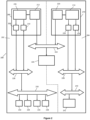
- FIG. 1 schematically shows an integrated circuit 100 according to a first embodiment of the present disclosure.
- the integrated circuit 100 comprises a first processing core 102 and a second processing core 104.
- Each processing core 102, 104 is operable to execute instructions to perform processing tasks for applications. It will be appreciated that the use of the designations "first” and “second” herein is only to improve legibility and does not imply any hierarchy, unless otherwise stated.
- the first processing core 102 comprises a first core controller 106 which is connected to a first memory resource 108 and to a first hardware accelerator module 110.
- the first memory resource 108 is not directly connected to the first hardware accelerator module 110; instead, the first hardware accelerator module 110 may only obtain data from the first memory resource 108 via the first core controller 106.
- the second processing core 104 comprises a second core controller 112 which is connected to a second memory resource 114 and to a second hardware accelerator module 116.
- the second memory resource 114 is not directly connected to the second hardware accelerator module 116; instead, the second hardware accelerator module 116 may only obtain data from the second memory resource 114 via the second core controller 112.
- the integrated circuit 100 further comprises a shared bus 118 configured to allow communication between the two processing cores 102, 104 (which are otherwise isolated from one another) via the hardware accelerator modules 110, 116.
- the shared bus 118 is connected to a shared memory resource 120 and to the first and the second hardware accelerator modules 110, 116.
- data retrieved from the first memory resource 108 may be shared with the second processing core 104; and data retrieved from the second memory resource 114 may be shared with the first processing core 102.
- data retrieved from the shared memory resource 120 may be shared with either of the processing cores 102, 104.
- the two processing cores 102, 104 are configured to process different applications, preferably simultaneously.
- the two processing cores 102, 104 are heterogeneous, that is to say the two processing cores 102, 104 are configured differently from one another.
- the first processing core 102 has a faster clock frequency than the second processing core 104.
- the second processing core 104 has a faster clock frequency that the first processing core 102.
- the core controller 106 is a different type of controller to the core controller 112.
- the first memory resource 108 is configured differently to the second memory resource 114. It will be appreciated, however, that in other embodiments, the two processing cores 102, 104 (and/or individual components thereof) may have the same configuration.
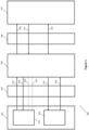
- FIG. 2 schematically shows an integrated circuit according to a second embodiment of the present disclosure.
- the integrated circuit 200 comprises a first subsystem 202 and a second subsystem 204.
- the first subsystem 202 comprises a processing core 260 comprising a core controller 206.
- the core controller 206 is connected to an instruction memory resource 208 and a data memory resource 210.
- the core controller 206 is also connected to a hardware accelerator module 212.
- the memory resources 208, 210 are not directly connected to the hardware accelerator module 212.
- the data memory resource is a tightly integrated data memory.
- the instruction memory resource is a tightly integrated instruction memory.
- the first subsystem 202 further comprises a dedicated system bus 226 which is connected between the processing core 260 and a peripherals bus 230.
- the system bus 226 may be connected to the processing core 260 and peripherals bus 230 by means of a crossbar connection; in other words, using a grid of connections. In this way, contention in the subsystem can be minimised since multiple alternative paths are provided on the system bus 226.
- the peripherals bus 230 is configured to be connected to one or more peripheral resources 232, 234, 236, 238.
- the peripheral resources may include interfaces to other systems or subsystems, e.g. within an avionics system.
- the peripheral resources 232, 234, 236, 238 may include a CAN bus, a Serial Peripheral Interface (SPI), an I2C interface or an ARINC 429 interface.
- the peripheral resources 232, 234, 236, 238 may include one or more external memory resources.
- the second subsystem 204 comprises a processing core 270 comprising a core controller 214.
- the core controller 214 is connected to an instruction memory resource 216 and a data memory resource 218.
- the core controller 214 is also connected to a hardware accelerator module 220.
- the memory resources 216, 218 are not directly connected to the hardware accelerator module 220.
- the second subsystem 204 further comprises a system bus 228 which is connected between the processing core 270 and a memory bus 240.
- the system bus 228 may be connected to the processing core 270 and memory bus 240 by means of a crossbar connection; in other words, using a grid of connections. In this way, contention in the subsystem can be minimised since multiple alternative paths are provided on the system bus 228.
- the memory bus 240 is configured to be connected to one or more memory resources 242.
- the one or more memory resources 242 may include one or more external memory resources.
- the one or more memory resources 242 may comprise a scratchpad memory.
- the integrated circuit 200 also comprises a shared bus 222 and a shared memory resource 224.
- the first and second subsystems 202, 204 are isolated from one another such that the only communication path between the two subsystems 202, 204 is via the hardware accelerator modules 212, 220 and the shared bus 222.
- dedicated resources e.g. dedicated memory resources, dedicated system bus
- FIG. 3 schematically shows communication between a processing core 302, a hardware accelerator module 306 and a shared bus 310 in an integrated circuit 300 according to the present disclosure.
- the communication between the processing core 302 and the hardware accelerator module 306 takes place via an interface 304.
- the interface 304 is a Custom Instructions Interface. Any suitable and desired Custom Instructions Interface may be used in accordance with the invention.
- the interface 304 may be an RoCC interface.
- any suitable and desired embedded processor that supports such a Custom Instructions Interface may be used in connection with the subject-matter disclosed herein.
- suitable embedded processors include Intel Nios II, Xilinx MicroBlaze, etc.
- the communication between the hardware accelerator module 306 and the shared bus 310 takes place via a further interface 308.
- the further interface 308 may be any suitable and desired interface.
- the further interface 308 illustrated in figure 3 is configured to operate using standard bus protocol. In an embodiment, the further interface 308 operates using the known TileLink bus.
- the hardware accelerator module 306 is configured to perform cryptographic operations for the processing core 302. In an embodiment, the hardware accelerator module 306 encrypts data provided by the processing core 302 before forwarding the encrypted data to the shared bus 310. In an embodiment, the hardware accelerator module 306 decrypts data provided via the shared bus 310 and forwards the decrypted data to the processing core 302. Secure sharing of data between processing cores can thus be ensured. It will of course be appreciated that the hardware accelerator module 306 may also forward encrypted data, for example in the event that data is to be sent to an external communication interface.
- the processing core 302 comprises a core controller 312 configured to send an instruction signal 316 to the hardware accelerator module 306 via interface 304.
- the instructions are instructions from the known RISC-V instruction set. Using an open instruction set such as RISC-V makes it possible to reduce the time spent developing, testing and verifying custom system-on-chip architectures. It also makes it possible to introduce custom instructions at the microarchitecture level.
- a further advantage of using known instructions sets such as RISC-V with known protocols such as the ROCC protocol is that this provides improved visibility over the system behaviour. Formal verification of the system operation can be facilitated as a result, and certification becomes less onerous than in systems to date. Confidence in the ability of the system to handle high criticality applications in a secure manner can be improved as a result of the intense verification process and relative ease of certification as a result of the improved oversight.
- the core controller 312 is also configured to send a verification signal 320 to the hardware accelerator module 306 to prove that the instruction signal 316 is a valid instructions signal. In this way, the hardware accelerator module 306 can determine whether or not the instructions received from the core controller 312 are from the intended application. In the event of an external attack on the processing core 302, the verification signal 320 would indicate that the instruction signal 316 is not to be trusted. By providing the hardware accelerator module 306 between the core controller 212 and the shared bus 310, an extra layer of security is therefore provided as the shared bus 310 cannot be accessed except through the hardware accelerator module 306.
- the hardware accelerator module 306 is configured to send a signal 322 to indicate when it is ready to receive instructions from the processing core 302. In other embodiments, the hardware accelerator module 306 may instead or additionally be configured to send a signal when it is unable to receive instructions from the processing core 302.
- the hardware accelerator module 306 may send a request for data 330 to the shared bus 310 via further interface 308.
- the shared bus 310 is connected to a shared memory resource. Data retrieved from the shared memory resource can be sent via the shared bus 310 and the further interface 308 to the hardware accelerator module 306. In particular, data may be sent via signal 332 from the shared bus 310.
- a verification signal may also be sent from the shared bus 310 to the hardware accelerator module 306 in order to verify the data being sent via signal 332. In this way, in the event of an external attack on the shared system resources (i.e. shared bus 308 and shared memory resource), access to the processing core 302 can be denied as the hardware accelerator module 306 will not pass the data through if the correct verification signal has not been received.
- the hardware accelerator module 306 When the correct verification signal is received by the hardware accelerator module 306 (e.g. when the hardware accelerator module 306 has determined that the verification signal received via the further interface 308 is correct), the hardware accelerator module 306 passes the data retrieved from the shared memory resource to the processing core 302 via the interface 304 using response signal 318. The provided data can then be used by the core controller 312 as required.
- the processing core 302 also comprises a memory resource 314. In some applications, it may be desirable for the processing core 302 to provide data to the shared memory resource for use by the other of the two processing cores of the integrated circuit 300.
- the processing core 312 sends an instruction signal 316 to the hardware accelerator module 306 to cause the hardware accelerator module 306 to send a data request signal 324 to the memory resource 314.
- the instruction signal 316 can be verified (validated) by the hardware accelerator module 306 using the verification signal 320 as described above.
- the memory resource 314 sends a data signal 328 containing the requested data to the hardware accelerator module 306.
- the hardware accelerator module 306 forwards the requested data to the shared bus 310 via the further interface 308 using a further data signal 334.
- the data can then be accessed by the other processing core of the integrated circuit 300 via the shared bus 310 and the corresponding hardware accelerator module of the other processing core.
- the hardware accelerator module 306 sends an interrupt via the shared bus 310 to the other processing core of the integrated circuit 300 to indicate that the data is available to access via the shared bus.
- figure 3 shows only the communication paths for one processing core of the two provided on an integrated circuit 300 according to the present disclosure.
- the communication paths for the other processing core are similar, preferably identical, to those depicted in figure 3 .
Landscapes
- Engineering & Computer Science (AREA)
- Theoretical Computer Science (AREA)
- General Engineering & Computer Science (AREA)
- Computer Hardware Design (AREA)
- Physics & Mathematics (AREA)
- General Physics & Mathematics (AREA)
- Computing Systems (AREA)
- Microelectronics & Electronic Packaging (AREA)
- Multi Processors (AREA)
Abstract
Description
- The present disclosure relates generally to integrated circuits and, in particular, to integrated circuits for high criticality applications.
- The need for improved performance and dependability is becoming a reality in all embedded computing systems. Autonomy, security, or enhanced data analytics for embedded Prognostics and Health Monitoring (PHM), among others, are imposing the use of new and a higher number of sensors and communication capabilities. Safety and/or security is often not a primary objective in the design of commercial general-purpose processors.
- The inventors have realised that there is a need for an improved integrated circuit for high-criticality applications.
- The present disclosure relates to an integrated circuit comprising: two processing cores, wherein each processing core comprises: a core controller operable to execute instructions to perform processing tasks; a memory resource connected to the core controller; and a hardware accelerator module connected to the core controller; wherein the integrated circuit further comprises: a shared bus connected to the respective hardware accelerator modules of the two processing cores; and a shared memory resource connected to the shared bus; and wherein the only communication path between the two processing cores is via the hardware accelerator modules and the shared bus.
- In an embodiment, the two processing cores may be heterogeneous.
- In an embodiment, the clock frequency of one of the two processing cores may be faster than the clock frequency of the other one of the two processing cores.
- In an embodiment, the integrated circuit may further comprise two isolated subsystems; wherein each processing core is associated with a respective subsystem; wherein each subsystem comprises a dedicated system bus configured to connect the respective associated processing core to components of the subsystem; and wherein the system bus of a respective subsystem is isolated from the system bus of the respective other subsystem.
- In an embodiment, each system bus may be connected to the respective associated processing core by means of a crossbar connection.
- In an embodiment, a first one of the two subsystems may further comprise an external memory bus configured to be connected to an external memory resource.
- In an embodiment, a second one of the two subsystems may further comprise a peripherals bus configured to be connected to one or more peripheral resources.
- In an embodiment, the memory resource of each processing core may comprise a data memory resource and an instruction memory resource.
- In an embodiment, the data memory resource may be a tightly integrated data memory.
- In an embodiment, the instruction memory resource may be a tightly integrated instruction memory.
- In an embodiment, the hardware accelerator module of each processing core may be configured to perform cryptographic operations.
- In an embodiment, the hardware accelerator module of each processing core may be configured to execute instructions from the RISC-V instruction set.
- In an embodiment, the hardware accelerator module of each processing core may be configured to communicate with its associated processing core using a custom instruction interface.
- In an embodiment, the hardware accelerator module is configured to provide data from the memory resource of one of the two processing cores to the shared memory resource via the shared bus.
- In an embodiment, the hardware accelerator module is further configured to send an interrupt to the other one of the two processing cores to indicate that new data is available in the shared memory resource.
- Features of any aspect or embodiment described herein may, wherever appropriate, be applied to any other aspect or embodiment described herein. Where reference is made to different embodiments or sets of embodiments, it should be understood that these are not necessarily distinct but may overlap.
- Certain embodiments of the present disclosure will now be described in greater detail by way of example only and with reference to the accompanying drawings, in which:
-
Figure 1 schematically shows an integrated circuit according to a first embodiment of the present disclosure; -
Figure 2 schematically shows an integrated circuit according to a second embodiment of the present disclosure; and -
Figure 3 schematically shows communication between a processing core and the shared bus of an integrated circuit according to a third embodiment of the present disclosure. - The technology described herein may be useful in avionics applications
- An integrated circuit as disclosed herein comprises: two processing cores, wherein each processing core comprises: a core controller operable to execute instructions to perform processing tasks; a memory resource connected to the core controller; and a hardware accelerator module connected to the core controller; wherein the integrated circuit further comprises: a shared bus connected to the respective hardware accelerator modules of the two processing cores; and a shared memory resource connected to the shared bus; and wherein the only communication path between the two processing cores is via the hardware accelerator modules and the shared bus.
- By providing two isolated subsystems where the only communication path between the respective processing cores of the isolated subsystems is via the hardware accelerator modules and the shared bus, it is possible to provide improved security. In particular, in the event of an external attack on one of the two cores, the isolation of the other core makes it possible for that core to continue to operate safely. In addition, the isolated nature of the two subsystems make it possible to ensure confidentiality of assets between the two subsystems.
- The duplication of resources (e.g. providing a respective memory resource for each subsystem) and the isolation of the two subsystems makes it possible to provide more robust systems. For example, in the event of a fault in one subsystem, the other subsystem may continue running since it has its own resources which are isolated from those of the subsystem which has experienced the fault. The separation of the two memory resources in the system (i.e. the respective memory resources for each of the subsystems) allows a fault in one memory resource to be contained in that memory resource in the one subsystem while the other subsystem continues to operate.
- A further advantage of the integrated circuits described herein is the reduction of contention in the system owing to the dedicated resources provided for each processing core or subsystem. By providing dedicated resources for each processing core or subsystem, it is possible to reduce the occurrence of, or entirely avoid, any situation in which two cores are competing for the same resource. As such, the time determinism within the system can be improved as it is not necessary to take contention into account. Processing time for particular tasks can therefore be more accurately predicted since each command can be expected to take a prescribed amount of time for that command and it can be determined when each command will be executed. This is in contrast to systems in which contention is present since in such systems it is not possible to determine when a command will be executed owing to contention causing possible delays in the system, e.g. in data retrieval.
-
Figure 1 schematically shows anintegrated circuit 100 according to a first embodiment of the present disclosure. Theintegrated circuit 100 comprises afirst processing core 102 and asecond processing core 104. Eachprocessing core - The
first processing core 102 comprises afirst core controller 106 which is connected to afirst memory resource 108 and to a firsthardware accelerator module 110. Thefirst memory resource 108 is not directly connected to the firsthardware accelerator module 110; instead, the firsthardware accelerator module 110 may only obtain data from thefirst memory resource 108 via thefirst core controller 106. - Similarly, the
second processing core 104 comprises asecond core controller 112 which is connected to asecond memory resource 114 and to a secondhardware accelerator module 116. Thesecond memory resource 114 is not directly connected to the secondhardware accelerator module 116; instead, the secondhardware accelerator module 116 may only obtain data from thesecond memory resource 114 via thesecond core controller 112. - The
integrated circuit 100 further comprises a sharedbus 118 configured to allow communication between the twoprocessing cores 102, 104 (which are otherwise isolated from one another) via thehardware accelerator modules bus 118 is connected to a sharedmemory resource 120 and to the first and the secondhardware accelerator modules bus 118, data retrieved from thefirst memory resource 108 may be shared with thesecond processing core 104; and data retrieved from thesecond memory resource 114 may be shared with thefirst processing core 102. In addition, data retrieved from the sharedmemory resource 120 may be shared with either of theprocessing cores - The two
processing cores processing cores processing cores first processing core 102 has a faster clock frequency than thesecond processing core 104. In another embodiment, thesecond processing core 104 has a faster clock frequency that thefirst processing core 102. In an embodiment, thecore controller 106 is a different type of controller to thecore controller 112. In an embodiment, thefirst memory resource 108 is configured differently to thesecond memory resource 114. It will be appreciated, however, that in other embodiments, the twoprocessing cores 102, 104 (and/or individual components thereof) may have the same configuration. -
Figure 2 schematically shows an integrated circuit according to a second embodiment of the present disclosure. Theintegrated circuit 200 comprises afirst subsystem 202 and asecond subsystem 204. - The
first subsystem 202 comprises aprocessing core 260 comprising acore controller 206. Thecore controller 206 is connected to aninstruction memory resource 208 and adata memory resource 210. Thecore controller 206 is also connected to ahardware accelerator module 212. Thememory resources hardware accelerator module 212. In an embodiment, the data memory resource is a tightly integrated data memory. In an embodiment, the instruction memory resource is a tightly integrated instruction memory. By providing one or more tightly integrated memory resources, time determinism in thesubsystems - The
first subsystem 202 further comprises adedicated system bus 226 which is connected between theprocessing core 260 and aperipherals bus 230. In an embodiment, thesystem bus 226 may be connected to theprocessing core 260 andperipherals bus 230 by means of a crossbar connection; in other words, using a grid of connections. In this way, contention in the subsystem can be minimised since multiple alternative paths are provided on thesystem bus 226. - The
peripherals bus 230 is configured to be connected to one or moreperipheral resources peripheral resources peripheral resources - The
second subsystem 204 comprises aprocessing core 270 comprising acore controller 214. Thecore controller 214 is connected to aninstruction memory resource 216 and adata memory resource 218. Thecore controller 214 is also connected to ahardware accelerator module 220. Thememory resources hardware accelerator module 220. - The
second subsystem 204 further comprises asystem bus 228 which is connected between theprocessing core 270 and amemory bus 240. In an embodiment, thesystem bus 228 may be connected to theprocessing core 270 andmemory bus 240 by means of a crossbar connection; in other words, using a grid of connections. In this way, contention in the subsystem can be minimised since multiple alternative paths are provided on thesystem bus 228. - The
memory bus 240 is configured to be connected to one ormore memory resources 242. The one ormore memory resources 242 may include one or more external memory resources. The one ormore memory resources 242 may comprise a scratchpad memory. - The
integrated circuit 200 also comprises a sharedbus 222 and a sharedmemory resource 224. The first andsecond subsystems subsystems hardware accelerator modules bus 222. By providing each of the subsystems with dedicated resources (e.g. dedicated memory resources, dedicated system bus), it is possible to reduce or avoid contention within the system since the two processing cores do not compete with one another for access to those resources. -
Figure 3 schematically shows communication between aprocessing core 302, ahardware accelerator module 306 and a sharedbus 310 in anintegrated circuit 300 according to the present disclosure. The communication between theprocessing core 302 and thehardware accelerator module 306 takes place via aninterface 304. In an embodiment, theinterface 304 is a Custom Instructions Interface. Any suitable and desired Custom Instructions Interface may be used in accordance with the invention. For example, theinterface 304 may be an RoCC interface. It will further be appreciated that any suitable and desired embedded processor that supports such a Custom Instructions Interface may be used in connection with the subject-matter disclosed herein. Some examples of suitable embedded processors include Intel Nios II, Xilinx MicroBlaze, etc. - The communication between the
hardware accelerator module 306 and the sharedbus 310 takes place via afurther interface 308. Thefurther interface 308 may be any suitable and desired interface. Thefurther interface 308 illustrated infigure 3 is configured to operate using standard bus protocol. In an embodiment, thefurther interface 308 operates using the known TileLink bus. - The
hardware accelerator module 306 is configured to perform cryptographic operations for theprocessing core 302. In an embodiment, thehardware accelerator module 306 encrypts data provided by theprocessing core 302 before forwarding the encrypted data to the sharedbus 310. In an embodiment, thehardware accelerator module 306 decrypts data provided via the sharedbus 310 and forwards the decrypted data to theprocessing core 302. Secure sharing of data between processing cores can thus be ensured. It will of course be appreciated that thehardware accelerator module 306 may also forward encrypted data, for example in the event that data is to be sent to an external communication interface. - The
processing core 302 comprises acore controller 312 configured to send aninstruction signal 316 to thehardware accelerator module 306 viainterface 304. In an embodiment, the instructions are instructions from the known RISC-V instruction set. Using an open instruction set such as RISC-V makes it possible to reduce the time spent developing, testing and verifying custom system-on-chip architectures. It also makes it possible to introduce custom instructions at the microarchitecture level. - A further advantage of using known instructions sets such as RISC-V with known protocols such as the ROCC protocol is that this provides improved visibility over the system behaviour. Formal verification of the system operation can be facilitated as a result, and certification becomes less onerous than in systems to date. Confidence in the ability of the system to handle high criticality applications in a secure manner can be improved as a result of the intense verification process and relative ease of certification as a result of the improved oversight.
- The
core controller 312 is also configured to send averification signal 320 to thehardware accelerator module 306 to prove that theinstruction signal 316 is a valid instructions signal. In this way, thehardware accelerator module 306 can determine whether or not the instructions received from thecore controller 312 are from the intended application. In the event of an external attack on theprocessing core 302, theverification signal 320 would indicate that theinstruction signal 316 is not to be trusted. By providing thehardware accelerator module 306 between thecore controller 212 and the sharedbus 310, an extra layer of security is therefore provided as the sharedbus 310 cannot be accessed except through thehardware accelerator module 306. - In the embodiment depicted in
figure 3 , thehardware accelerator module 306 is configured to send asignal 322 to indicate when it is ready to receive instructions from theprocessing core 302. In other embodiments, thehardware accelerator module 306 may instead or additionally be configured to send a signal when it is unable to receive instructions from theprocessing core 302. - When the
hardware accelerator module 306 receives theinstruction signal 316 and determines that it is valid based on theverification signal 320, thehardware accelerator module 306 may send a request fordata 330 to the sharedbus 310 viafurther interface 308. As illustrated infigures 1 and2 , the sharedbus 310 is connected to a shared memory resource. Data retrieved from the shared memory resource can be sent via the sharedbus 310 and thefurther interface 308 to thehardware accelerator module 306. In particular, data may be sent via signal 332 from the sharedbus 310. Although not illustrated, it will be appreciated that a verification signal may also be sent from the sharedbus 310 to thehardware accelerator module 306 in order to verify the data being sent via signal 332. In this way, in the event of an external attack on the shared system resources (i.e. sharedbus 308 and shared memory resource), access to theprocessing core 302 can be denied as thehardware accelerator module 306 will not pass the data through if the correct verification signal has not been received. - When the correct verification signal is received by the hardware accelerator module 306 (e.g. when the
hardware accelerator module 306 has determined that the verification signal received via thefurther interface 308 is correct), thehardware accelerator module 306 passes the data retrieved from the shared memory resource to theprocessing core 302 via theinterface 304 usingresponse signal 318. The provided data can then be used by thecore controller 312 as required. - The
processing core 302 also comprises amemory resource 314. In some applications, it may be desirable for theprocessing core 302 to provide data to the shared memory resource for use by the other of the two processing cores of theintegrated circuit 300. In an embodiment, theprocessing core 312 sends aninstruction signal 316 to thehardware accelerator module 306 to cause thehardware accelerator module 306 to send adata request signal 324 to thememory resource 314. Theinstruction signal 316 can be verified (validated) by thehardware accelerator module 306 using theverification signal 320 as described above. - In response to receiving the data request signal 324 from the
hardware accelerator module 306, thememory resource 314 sends adata signal 328 containing the requested data to thehardware accelerator module 306. In response to receiving the data signal 328 from thememory resource 314, thehardware accelerator module 306 forwards the requested data to the sharedbus 310 via thefurther interface 308 using afurther data signal 334. The data can then be accessed by the other processing core of theintegrated circuit 300 via the sharedbus 310 and the corresponding hardware accelerator module of the other processing core. In an embodiment, thehardware accelerator module 306 sends an interrupt via the sharedbus 310 to the other processing core of theintegrated circuit 300 to indicate that the data is available to access via the shared bus. - It will be appreciated that
figure 3 shows only the communication paths for one processing core of the two provided on anintegrated circuit 300 according to the present disclosure. In an embodiment, the communication paths for the other processing core are similar, preferably identical, to those depicted infigure 3 . - It will further be appreciated that although the
integrated circuits - It will further be appreciated by those skilled in the art that the invention has been illustrated by describing one or more specific embodiments thereof, but is not limited to these embodiments; many variations and modifications are possible, within the scope of the accompanying claims.
Claims (15)
- An integrated circuit comprising:
two processing cores, wherein each processing core comprises:a core controller operable to execute instructions to perform processing tasks;a memory resource connected to the core controller; anda hardware accelerator module connected to the core controller;wherein the integrated circuit further comprises:a shared bus connected to the respective hardware accelerator modules of the two processing cores; anda shared memory resource connected to the shared bus; andwherein the only communication path between the two processing cores is via the hardware accelerator modules and the shared bus. - The integrated circuit of claim 1, wherein the two processing cores are heterogeneous.
- The integrated circuit of claim 2, wherein the clock frequency of one of the two processing cores is faster than the clock frequency of the other one of the two processing cores.
- The integrated circuit of any preceding claim, further comprising two isolated subsystems;wherein each processing core is associated with a respective subsystem;wherein each subsystem comprises a dedicated system bus configured to connect the respective associated processing core to components of the subsystem; andwherein the system bus of a respective subsystem is isolated from the system bus of the respective other subsystem.
- The integrated circuit of claim 4, wherein each system bus is connected to the respective associated processing core by means of a crossbar connection.
- The integrated circuit of claim 4 or 5, wherein a first one of the two subsystems further comprises an external memory bus configured to be connected to an external memory resource.
- The integrated circuit of any of claims 4, 5 and 6, wherein a second one of the two subsystems further comprises a peripherals bus configured to be connected to one or more peripheral resources.
- The integrated circuit of any preceding claim, wherein the memory resource of each processing core comprises a data memory resource and an instruction memory resource.
- The integrated circuit of claim 8, wherein the data memory resource is a tightly integrated data memory.
- The integrated circuit of claim 8 or 9, wherein the instruction memory resource is a tightly integrated instruction memory.
- The integrated circuit of any preceding claim, wherein the hardware accelerator module of each processing core is configured to perform cryptographic operations.
- The integrated circuit of any preceding claim, wherein the hardware accelerator module of each processing core is configured to execute instructions from the RISC-V instruction set.
- The integrated circuit of claim 12, wherein the hardware accelerator module of each processing core is configured to communicate with its associated processing core using a custom instruction interface.
- The integrated circuit of any preceding claim, wherein the hardware accelerator module is configured to provide data from the memory resource of one of the two processing cores to the shared memory resource via the shared bus.
- The integrated circuit of claim 14, wherein the hardware accelerator module is further configured to send an interrupt to the other one of the two processing cores to indicate that new data is available in the shared memory resource.
Priority Applications (2)
| Application Number | Priority Date | Filing Date | Title |
|---|---|---|---|
| EP23176157.8A EP4471610A1 (en) | 2023-05-30 | 2023-05-30 | Integrated circuit |
| US18/672,994 US20240403252A1 (en) | 2023-05-30 | 2024-05-23 | Integrated circuit |
Applications Claiming Priority (1)
| Application Number | Priority Date | Filing Date | Title |
|---|---|---|---|
| EP23176157.8A EP4471610A1 (en) | 2023-05-30 | 2023-05-30 | Integrated circuit |
Publications (1)
| Publication Number | Publication Date |
|---|---|
| EP4471610A1 true EP4471610A1 (en) | 2024-12-04 |
Family
ID=86609735
Family Applications (1)
| Application Number | Title | Priority Date | Filing Date |
|---|---|---|---|
| EP23176157.8A Pending EP4471610A1 (en) | 2023-05-30 | 2023-05-30 | Integrated circuit |
Country Status (2)
| Country | Link |
|---|---|
| US (1) | US20240403252A1 (en) |
| EP (1) | EP4471610A1 (en) |
Citations (3)
| Publication number | Priority date | Publication date | Assignee | Title |
|---|---|---|---|---|
| US20080066074A1 (en) * | 2006-09-12 | 2008-03-13 | Mark Richard Nutter | System and Method for Securely Saving a Program Context to a Shared Memory |
| WO2008067918A1 (en) * | 2006-12-05 | 2008-06-12 | Telefonaktiebolaget Lm Ericsson (Publ) | Methods and devices for cache enhancing |
| US20200293667A1 (en) * | 2019-03-12 | 2020-09-17 | Samsung Electronics Co., Ltd. | Electronic device including secure integrated circuit |
Family Cites Families (5)
| Publication number | Priority date | Publication date | Assignee | Title |
|---|---|---|---|---|
| US8332653B2 (en) * | 2004-10-22 | 2012-12-11 | Broadcom Corporation | Secure processing environment |
| US9727388B2 (en) * | 2011-12-29 | 2017-08-08 | Intel Corporation | Migrating threads between asymmetric cores in a multiple core processor |
| WO2019067056A1 (en) * | 2017-09-28 | 2019-04-04 | Apple Inc. | Methods and architectures for secure ranging |
| US20240020150A1 (en) * | 2022-07-18 | 2024-01-18 | Nxp Usa, Inc. | System on Chip Isolation Control Architecture |
| US20240273334A1 (en) * | 2023-02-14 | 2024-08-15 | Efinix, Inc. | Neural network accelerator architecture based on custom instruction on fpga |
-
2023
- 2023-05-30 EP EP23176157.8A patent/EP4471610A1/en active Pending
-
2024
- 2024-05-23 US US18/672,994 patent/US20240403252A1/en active Pending
Patent Citations (3)
| Publication number | Priority date | Publication date | Assignee | Title |
|---|---|---|---|---|
| US20080066074A1 (en) * | 2006-09-12 | 2008-03-13 | Mark Richard Nutter | System and Method for Securely Saving a Program Context to a Shared Memory |
| WO2008067918A1 (en) * | 2006-12-05 | 2008-06-12 | Telefonaktiebolaget Lm Ericsson (Publ) | Methods and devices for cache enhancing |
| US20200293667A1 (en) * | 2019-03-12 | 2020-09-17 | Samsung Electronics Co., Ltd. | Electronic device including secure integrated circuit |
Non-Patent Citations (1)
| Title |
|---|
| BRONLEEWE DAVID ET AL: "Runtime Encryption of Memory with Intel Total Memory...", 25 March 2023 (2023-03-25), pages 1 - 9, XP093289195, Retrieved from the Internet <URL:https://web.archive.org/web/20230325112131/https://www.intel.com/content/www/us/en/developer/articles/news/runtime-encryption-of-memory-with-intel-tme-mk.html> [retrieved on 20250624] * |
Also Published As
| Publication number | Publication date |
|---|---|
| US20240403252A1 (en) | 2024-12-05 |
Similar Documents
| Publication | Publication Date | Title |
|---|---|---|
| CN114600108B (en) | System and method for remote authentication and information independent trusted computing by heterogeneous processor through open connector | |
| KR101010801B1 (en) | Method and apparatus for determining access permission | |
| US20140223052A1 (en) | System and method for slave-based memory protection | |
| CA1303226C (en) | Node for servicing interrupt request messages on a pended bus | |
| CN101874245B (en) | Method and apparatus for delegation of secure operating mode access privilege from processor to peripheral | |
| EP3241149B1 (en) | Method to isolate real-time or safety-critical software and operating system from non-critical software and operating system | |
| CN112948321A (en) | Method for managing the operation of a system-on-chip and corresponding system-on-chip | |
| WO2015081011A1 (en) | Hardware virtualization module for exclusive controlled access to cpu | |
| CN116340243B (en) | A secure chip architecture with dual-core trusted execution | |
| CN114035842A (en) | Firmware configuration method, computing system configuration method, computing device and equipment | |
| US9940480B2 (en) | Securing delegated remote management with digital signature | |
| US20250307384A1 (en) | Security Resource Access Method For Integrated Circuit, And Electronic Device | |
| US20240403252A1 (en) | Integrated circuit | |
| EP3646216B1 (en) | Methods and devices for executing trusted applications on processor with support for protected execution environments | |
| JP7012915B2 (en) | controller | |
| US20240176863A1 (en) | System-on-chip including a resource isolation system and method for managing the corresponding resource isolation | |
| US7676608B1 (en) | System for extending Multiple Independent Levels of Security (MILS) partitioning to input/output (I/O) devices | |
| EP4042303A1 (en) | Hypervisor secure event handling at a processor | |
| Majumder et al. | Reliable flight control system architecture for agile airborne platforms: an asymmetric multiprocessing approach | |
| Nojiri et al. | Domain partitioning technology for embedded multicore processors | |
| JP2010146117A (en) | Information processor, information processing method and information processing program | |
| EP3258371B1 (en) | Communication regulation in computing systems | |
| EP4492242A2 (en) | Integrated circuit having safe communication between its functional units, corresponding communication method, electronic device and storage medium | |
| CN117056982B (en) | Multi-machine data signing verification method, system and storage medium | |
| Salamini et al. | A Design Flow to Securely Isolate FPGA Bus Transactions in Heterogeneous SoCs |
Legal Events
| Date | Code | Title | Description |
|---|---|---|---|
| PUAI | Public reference made under article 153(3) epc to a published international application that has entered the european phase |
Free format text: ORIGINAL CODE: 0009012 |
|
| STAA | Information on the status of an ep patent application or granted ep patent |
Free format text: STATUS: THE APPLICATION HAS BEEN PUBLISHED |
|
| AK | Designated contracting states |
Kind code of ref document: A1 Designated state(s): AL AT BE BG CH CY CZ DE DK EE ES FI FR GB GR HR HU IE IS IT LI LT LU LV MC ME MK MT NL NO PL PT RO RS SE SI SK SM TR |
|
| STAA | Information on the status of an ep patent application or granted ep patent |
Free format text: STATUS: REQUEST FOR EXAMINATION WAS MADE |
|
| STAA | Information on the status of an ep patent application or granted ep patent |
Free format text: STATUS: EXAMINATION IS IN PROGRESS |
|
| 17P | Request for examination filed |
Effective date: 20250604 |
|
| 17Q | First examination report despatched |
Effective date: 20250702 |