EP4471551A1 - Touch-control display panel and display apparatus - Google Patents
Touch-control display panel and display apparatus Download PDFInfo
- Publication number
- EP4471551A1 EP4471551A1 EP22960048.1A EP22960048A EP4471551A1 EP 4471551 A1 EP4471551 A1 EP 4471551A1 EP 22960048 A EP22960048 A EP 22960048A EP 4471551 A1 EP4471551 A1 EP 4471551A1
- Authority
- EP
- European Patent Office
- Prior art keywords
- base substrate
- signal line
- display panel
- touch
- signal lines
- Prior art date
- Legal status (The legal status is an assumption and is not a legal conclusion. Google has not performed a legal analysis and makes no representation as to the accuracy of the status listed.)
- Pending
Links
Images





Classifications
-
- H—ELECTRICITY
- H10—SEMICONDUCTOR DEVICES; ELECTRIC SOLID-STATE DEVICES NOT OTHERWISE PROVIDED FOR
- H10K—ORGANIC ELECTRIC SOLID-STATE DEVICES
- H10K59/00—Integrated devices, or assemblies of multiple devices, comprising at least one organic light-emitting element covered by group H10K50/00
- H10K59/40—OLEDs integrated with touch screens
-
- G—PHYSICS
- G06—COMPUTING OR CALCULATING; COUNTING
- G06F—ELECTRIC DIGITAL DATA PROCESSING
- G06F3/00—Input arrangements for transferring data to be processed into a form capable of being handled by the computer; Output arrangements for transferring data from processing unit to output unit, e.g. interface arrangements
- G06F3/01—Input arrangements or combined input and output arrangements for interaction between user and computer
- G06F3/03—Arrangements for converting the position or the displacement of a member into a coded form
- G06F3/041—Digitisers, e.g. for touch screens or touch pads, characterised by the transducing means
- G06F3/0416—Control or interface arrangements specially adapted for digitisers
- G06F3/04164—Connections between sensors and controllers, e.g. routing lines between electrodes and connection pads
-
- G—PHYSICS
- G06—COMPUTING OR CALCULATING; COUNTING
- G06F—ELECTRIC DIGITAL DATA PROCESSING
- G06F3/00—Input arrangements for transferring data to be processed into a form capable of being handled by the computer; Output arrangements for transferring data from processing unit to output unit, e.g. interface arrangements
- G06F3/01—Input arrangements or combined input and output arrangements for interaction between user and computer
- G06F3/03—Arrangements for converting the position or the displacement of a member into a coded form
- G06F3/041—Digitisers, e.g. for touch screens or touch pads, characterised by the transducing means
- G06F3/0412—Digitisers structurally integrated in a display
-
- G—PHYSICS
- G06—COMPUTING OR CALCULATING; COUNTING
- G06F—ELECTRIC DIGITAL DATA PROCESSING
- G06F3/00—Input arrangements for transferring data to be processed into a form capable of being handled by the computer; Output arrangements for transferring data from processing unit to output unit, e.g. interface arrangements
- G06F3/01—Input arrangements or combined input and output arrangements for interaction between user and computer
- G06F3/03—Arrangements for converting the position or the displacement of a member into a coded form
- G06F3/041—Digitisers, e.g. for touch screens or touch pads, characterised by the transducing means
- G06F3/044—Digitisers, e.g. for touch screens or touch pads, characterised by the transducing means by capacitive means
- G06F3/0442—Digitisers, e.g. for touch screens or touch pads, characterised by the transducing means by capacitive means using active external devices, e.g. active pens, for transmitting changes in electrical potential to be received by the digitiser
-
- H—ELECTRICITY
- H10—SEMICONDUCTOR DEVICES; ELECTRIC SOLID-STATE DEVICES NOT OTHERWISE PROVIDED FOR
- H10K—ORGANIC ELECTRIC SOLID-STATE DEVICES
- H10K59/00—Integrated devices, or assemblies of multiple devices, comprising at least one organic light-emitting element covered by group H10K50/00
- H10K59/10—OLED displays
- H10K59/12—Active-matrix OLED [AMOLED] displays
- H10K59/126—Shielding, e.g. light-blocking means over the TFTs
-
- H—ELECTRICITY
- H10—SEMICONDUCTOR DEVICES; ELECTRIC SOLID-STATE DEVICES NOT OTHERWISE PROVIDED FOR
- H10K—ORGANIC ELECTRIC SOLID-STATE DEVICES
- H10K59/00—Integrated devices, or assemblies of multiple devices, comprising at least one organic light-emitting element covered by group H10K50/00
- H10K59/10—OLED displays
- H10K59/12—Active-matrix OLED [AMOLED] displays
- H10K59/131—Interconnections, e.g. wiring lines or terminals
-
- G—PHYSICS
- G06—COMPUTING OR CALCULATING; COUNTING
- G06F—ELECTRIC DIGITAL DATA PROCESSING
- G06F2203/00—Indexing scheme relating to G06F3/00 - G06F3/048
- G06F2203/041—Indexing scheme relating to G06F3/041 - G06F3/045
- G06F2203/04102—Flexible digitiser, i.e. constructional details for allowing the whole digitising part of a device to be flexed or rolled like a sheet of paper
-
- G—PHYSICS
- G06—COMPUTING OR CALCULATING; COUNTING
- G06F—ELECTRIC DIGITAL DATA PROCESSING
- G06F2203/00—Indexing scheme relating to G06F3/00 - G06F3/048
- G06F2203/041—Indexing scheme relating to G06F3/041 - G06F3/045
- G06F2203/04107—Shielding in digitiser, i.e. guard or shielding arrangements, mostly for capacitive touchscreens, e.g. driven shields, driven grounds
Definitions
- the present disclosure relates to the field of touch display technology, and in particular to a touch display panel and a display apparatus.
- an AMOLED Active Matrix Organic Light-Emitting Diode
- the technology of directly forming a touch structure (Flexible Multi-Layer On Cell, FMLOC) on an encapsulation layer of an OLED (Organic Light-Emitting Diode) touch display panel may form a lighter and thinner display apparatus, and may be applied to a folded and rollable OLED display apparatus.
- FMLOC Flexible Multi-Layer On Cell
- Embodiments of the present disclosure provide a touch display panel and a display apparatus, and the specific solutions are as follows.
- the embodiments of the present disclosure provide a touch display panel, including: a base substrate; a plurality of display signal lines on one side of the base substrate; a plurality of light-emitting devices in an array on a side of the plurality of display signal lines away from the base substrate; a touch structure on a side of the plurality of light-emitting devices away from the base substrate; and a shielding layer between the plurality of display signal lines and the plurality of light-emitting devices, an orthographic projection of the shielding layer on the base substrate covers at least a part of an orthographic projection of the plurality of display signal lines on the base substrate.
- an orthographic projection of the plurality of display signal lines on the base substrate is within the orthographic projection of the shielding layer on the base substrate.
- the shielding layer is made of a conductive material, and is loaded with a constant voltage signal or is grounded.
- the shielding layer is made of Ti/Al/Ti, Cu or ITO.
- the touch display panel includes a display region and a frame region around the display region; the touch display panel further includes: a high voltage power line in the display region and extending to the frame region, and a low voltage power line in the frame region; and the touch display panel further includes a first conductive connection part and a second conductive connection part independent from each other in the frame region and in the same layer as the shielding layer; the first conductive connection part is electrically connected to the high voltage power line, and the second conductive connection part is electrically connected to the low voltage power line.
- the shielding layer has a mesh structure.
- the plurality of display signal lines include at least one of a data signal line, a scanning signal line, a reset signal line, and a light-emitting control signal line.
- the touch display panel further includes a gate electrode in the same layer as the light-emitting control signal line, and the orthographic projection of the shielding layer on the base substrate further covers an orthographic projection of the gate electrode on the base substrate.
- the data signal line is between the base substrate and the shielding layer
- the scanning signal line and the reset signal line are in the same layer and located between the data signal line and the base substrate
- the light-emitting control signal line is between the scanning signal line and the base substrate.
- the touch display panel further includes: a first planarization layer between the data signal line and the scanning signal line, a second planarization layer between the data signal line and the shielding layer, and a third planarization layer between the shielding layer and the plurality of light-emitting devices; and a shape of the third planarization layer is the same as that of the second planarization layer.
- the touch display panel further includes: an encapsulation layer between the plurality of light-emitting devices and the touch structure, a polarizer on a side of the touch structure away from the base substrate, an optical adhesive on a side of the polarizer away from the base substrate, and a cover plate on a side of the optical adhesive away from the base substrate.
- embodiments of the present disclosure further provide a touch display panel, including: a base substrate; a plurality of display signal lines on one side of the base substrate; a plurality of light-emitting devices in an array on a side of the plurality of display signal lines away from the base substrate; an encapsulation layer on a side of the plurality of light-emitting devices away from the base substrate; a touch structure on a side of the encapsulation layer away from the base substrate; and a shielding layer between the plurality of display signal lines and the touch structure, and an orthographic projection of the shielding layer on the base substrate covers at least a part of an orthographic projection of the plurality of display signal lines on the base substrate;
- the plurality of display signal lines include a first signal line and a second signal line, the first signal line is configured to input an alternating current signal, and the second signal line is configured to input a direct current signal; and an overlapping area between the orthographic projection of the shielding layer on the base substrate and an orthographic projection of the first signal line
- the first signal line includes at least one of a data signal line, a scanning signal line, a reset signal line, and a light-emitting control signal line
- the second signal line includes at least one of a high voltage power line, a low voltage power line, and an initialization signal line.
- Embodiments of the present disclosure further provide a display apparatus, which includes the touch display panel provided by the embodiments of the present disclosure.
- the display apparatus further includes a flexible circuit board, the flexible circuit board includes at least one ground pad and at least one constant voltage pad, and the shield layer is at least electrically connected to two ground pads, or two constant voltage pads, or one ground pad and one constant voltage pad.
- the display apparatus further includes an active stylus.
- a capacitive touch screen on the market today has a touch function with a stylus, in addition to the common touch function with a finger.
- the stylus may include a passive stylus or an active stylus.
- the active stylus has a small and naked pen point and has the functions such as pen pressure, suspension touch, button and the like, and thus has a wider application scene and prospect than the passive stylus.
- more and more touch screens for example an electronic product with a touch screen, such as a mobile phone, a notebook computer, or a tablet computer, or the like, are equipped with the active stylus, which has higher requirements on various performances of the active stylus.
- the characteristics of the active stylus including accuracy, a signal-to-noise ratio (SNR), and a hover height, need to be improved.
- SNR signal-to-noise ratio
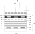
- the touch screen includes a display panel 1, an encapsulation layer 2, a touch structure 3, a polarizer 4, an optical adhesive 5 and a cover plate 6, which are sequentially stacked. That is, the touch structure 3 is directly formed on the encapsulation layer 2 on the display panel 1, and may adopt a metal mesh structure. That is, driving electrodes Tx and sensing electrodes Rx are located in the same layer, and are cooperated with a touch IC to realize the touch function.
- the display panel 1 includes a base substrate 11, an active layer 12, a gate insulating layer 13, a first gate layer 14, a first insulating layer 15, a second gate layer 16, an interlayer insulating layer 17, a first source-drain metal layer 18, a first planarization layer 19, a second source-drain metal layer 21 (provided with signal lines such as data signal lines therein), a second planarization layer 22, and a plurality of light-emitting devices, which are sequentially stacked.
- Each light-emitting device includes an anode 231, a luminescent layer 232, and a cathode 233, which are sequentially arranged, and the cathode 233 is closer to the encapsulation layer 2. As shown in FIG.
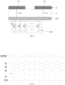
- FIG. 2 is a schematic diagram of a coupling noise model corresponding to a display module shown in FIG. 1 .
- FIG. 3 is a schematic diagram showing signal waveforms of data signal lines (S1, S2, S3 ?? Sn), a cathode 233 and the like. As may be seen from FIG. 3 , data signal jumps (including jumps from high to low, and from low to high) may be generated during the row refresh, and data signals in the data signal lines (S1, S2, S3 —
- the Data jump in FIG. 4 means that (a spike of) the coupling noise between the cathode 233 and the driving electrodes Tx and the sensing electrodes Rx is large due to the large voltage fluctuation generated at the data signal jumps.
- the active stylus point is small (about 1 mm)
- the coupling signal quantity between the active stylus point and the driving electrodes Tx and the sensing electrodes Rx is very small, and the active stylus has a synchronization function with the smaller signal quantity in a Hover state besides the conventional writing in a contact mode, so if the coupling noise is large, the active stylus function cannot be realized in the large-sized OLED.
- FIG. 5 is a schematic cross-sectional view of a touch display panel
- FIG. 6 is a schematic plan view of a touch display panel without a shielding layer
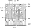
- FIG. 7 is a schematic plan view of a touch display panel with a shielding layer.
- FIG. 5 is a schematic cross-sectional view of the touch display panel along a CC' line in FIG. 7 .
- the touch display panel includes following components:
- the display signal lines 20 may include at least one of data signal lines 203 (Data), scanning signal lines 202 (Gate), reset signal lines 202' (Reset), and light-emitting control signal lines 201 (EM), where signals loaded on these signal lines are all alternating current signals (i.e., signals jumping from high to low and from low to high).
- the jumping signals may cause large voltage fluctuation, so that a voltage of the cathode (which will be described below) of the light-emitting device 30 is unstable.
- each data signal line 203 is configured to provide a display data signal for the touch display panel
- each scanning signal line 202 is configured to provide a display driving signal for the touch display panel
- each reset signal line 202' is configured to provide a reset signal for the touch display panel
- each light-emitting control signal line 201 is configured to provide a light-emitting control signal for the touch display panel.
- the light-emitting devices 30 may include a red (R) light-emitting device, a green (G) light-emitting device, and a blue (B) light-emitting device.
- Each light-emitting device 30 includes an anode 301, a luminescent layer 302, and a cathode 303, which are sequentially stacked.
- the anodes 301 of all the light-emitting devices 30 may be arranged independently of each other, and all the light-emitting devices 30 may share one cathode 303 (i.e., the cathode is arranged on an entire surface).
- the touch structure 40 may include driving electrodes Tx and sensing electrodes Rx, which are insulated from each other and arranged in a crossing manner and in the same layer.
- the shielding layer 50 may be made of a conductive material.
- the material of the shielding layer may be, but is not limited to, Ti/Al/Ti, Cu, ITO, or the like.
- a sheet resistance of the conductive material used to form the shielding layer should be as low as possible.
- the shielding layer 50 may be loaded with a constant voltage signal or be grounded.
- the shielding layer 50 is loaded with a constant voltage signal or is grounded, the interference of the signal jumps of the display signal lines 20 to the cathode 303 in the light-emitting devices 30 can be effectively shielded, and the stability of the voltage of the cathode 303 can be ensured, so that the coupling noise between the cathode 303 and the driving electrodes Tx and the sensing electrodes Rx in the touch structure 40 can be reduced.
- the shielding layer 50 covering the display signal lines 20 is provided between the display signal lines 20 and the light-emitting devices 30, so that the interference of the signal jumps of the display signal lines 20 to the cathode 303 in the light-emitting devices 30 can be effectively shielded, and the stability of the voltage of the cathode can be ensured, so that the coupling noise between the cathode and the driving electrodes Tx and the sensing electrodes Rx can be reduced and the signal-to-noise ratio of the touch display panel is improved.
- an orthographic projection of the shielding layer 50 on the base substrate 10 covers an orthographic projection of each of the data signal line 203, the scanning signal line 202, the reset signal line 202', and the light-emitting control signal line 201 on the base substrate 10, so that the interference of all signal lines loaded with the alternating current signals to the cathode can be effectively avoided, the stability of the voltage of the cathode can be further improved, and the coupling noise between the cathode and the driving electrodes and the sensing electrodes can be minimized.
- an orthographic projection of the plurality of display signal lines 20 (the data signal lines 203, the scanning signal lines 202, the reset signal lines 202', and the light-emitting control signal lines 201) on the base substrate 10 is located within the orthographic projection of the shielding layer 50 on the base substrate 10.
- the interference of the jumping signals (alternating current signals) on the data signal lines 203, the scanning signal lines 202, the reset signal lines 202', and the light-emitting control signal lines 201 to the cathode can be completely shielded by the shielding layer 50.
- the data signal lines 203 are located between the base substrate 10 and the shielding layer 50, the scanning signal lines 202 and the reset signal lines 202' are disposed in the same layer and located between the data signal lines 203 and the base substrate 10, and the light-emitting control signal lines 201 are located between the scanning signal lines 202 and the base substrate 10.
- a layer where the light-emitting control signal lines 201 are located is a first gate metal layer (Gatel)
- a layer where the scanning signal lines 202 and the reset signal lines 202' are located is a first source drain metal layer (SD1)
- a layer where the data signal lines 203 are located is a second source drain metal layer (SD2).
- the touch display panel provided in the embodiment of the present disclosure further includes: a first planarization layer 61 located between the data signal lines 203 and the scanning signal lines 202, a second planarization layer 62 located between the data signal lines 203 and the shield layer 50, and a third planarization layer 63 located between the shield layer 50 and the light-emitting devices 30.
- a shape of the third planarization layer 63 is the same as that of the second planarization layer 62.
- a material and a thickness of the third planarization layer 63 may or may not be the same as those of the second planarization layer 62.
- the touch display panel provided in the embodiment of the present disclosure further includes: a second gate metal layer 60 (Gate2) located between the light-emitting control signal lines 201 and the scanning signal lines 202.
- the second gate metal layer 60 is used for forming one plate of a storage capacitor in each pixel circuit of the display panel.
- the touch display panel provided in the embodiment of the present disclosure further includes: a fourth planarization layer 64 located between the light-emitting control signal lines 201 and the second gate metal layer 60, an interlayer insulating layer 65 located between the second gate metal layer 60 and the scanning signal lines 202, an active layer 70 located between the base substrate 10 and the light-emitting control signal lines 201, and a gate insulating layer 80 located between the active layer 70 and the light-emitting control signal lines 201.
- the touch display panel provided in the embodiment of the present disclosure further includes: an encapsulation layer 90 located between the light-emitting devices 30 and the touch structure 40, a polarizer 100 located on a side of the touch structure 40 away from the base substrate 10, an optical adhesive 101 located on a side of the polarizer 100 away from the base substrate 10, and a cover plate 102 located on a side of the optical adhesive 101 away from the base substrate 10.
- the encapsulation layer 90 may include a first inorganic layer, an organic layer, and a second inorganic layer stacked together, the optical adhesive 101 may be an OCA (Optically Clear Adhesive), and the cover plate may be a glass cover plate.
- OCA Optically Clear Adhesive
- the shielding layer 50 has a mesh structure.
- the shielding layer 50 only covers the display signal lines 20, without affecting an aperture ratio of the touch display panel.
- the scanning signal lines are generally electrically connected to gate driver circuits (gate driver on array, GOAs), and each signal output terminal of each GOA is configured to input a scanning driving signal to each scanning signal line.
- the scanning signal lines are electrically connected to gate electrodes of thin film transistors in the display panel, so that the stability of the voltage of the cathode is further affected by the signal jumps on the gate electrodes.
- the GOA jump refers to that the coupling noise (spike) between a cathode and the driving electrodes Tx and the sensing electrodes Rx is large due to the fluctuation of the voltage of the cathode caused by the jumping of the scanning driving signals.
- the touch display panel further includes gate electrodes 201' disposed in the same layer as the light-emitting control signal lines 201, and the orthographic projection of the shielding layer 50 on the base substrate 10 also covers an orthographic projection of the gate electrodes 201' on the base substrate 10. Therefore, the interference of the jumping signals on the gate electrodes 201' to the cathode in the light-emitting devices 30 can be shielded by the shielding layer 50, and the stability of the voltage of the cathode can be further ensured.
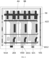
- the touch display panel has a display region AA and a frame region BB disposed around the display region AA.
- the touch display panel further includes: a high voltage power line VDD located in the display region AA and extending to the frame region BB, and a low voltage power line VSS located in the frame region BB.
- the low voltage power line VSS is generally disposed around the display region AA, and the low voltage power line VSS and the high voltage power line VDD are generally disposed in the same layer as the data signal line 203.
- the touch display panel further includes a first conductive connection part 1011 and a second conductive connection part 1012 located in the frame region BB independent from each other and in the same layer as the shielding layer 50.
- the first conductive connection part 1011 may be electrically connected to the high voltage power line VDD through a first via 621 penetrating through the second planarization layer 62 (not shown), and the second conductive connection part 1012 is electrically connected to the low voltage power line VSS through a second via 622 penetrating through the second planarization layer 62. Therefore, the display uniformity of the large-sized touch display panel can be improved by reducing the resistances of the high voltage power lines VDD or the low voltage power line VSS.
- FIG. 8 is only for schematically illustrating an electrical connection relationship between the first conductive connection part 1011 and the high voltage power lines VDD, and an electrical connection relationship between the second conductive connection part 1012 and the low voltage power line VSS.
- Patterns of the first conductive connection part 1011 electrically connected to the high voltage power lines VDD and the second conductive connection part 1012 electrically connected to the low voltage power line VSS are designed according to actual structures of the high voltage power line VDD and the low voltage power line VSS.
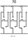
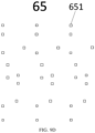
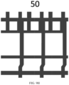
- FIGS. 9A to 9H are schematic diagrams of layout of layers in FIG. 7 .
- FIG. 9A is a schematic plan diagram of the active layer 70.
- FIG. 9B is a schematic plan diagram of the first gate metal layer (Gate1).
- the first gate metal layer (Gate1) includes the light-emitting control signal line 201, the gate electrodes 201', and the other plate 201" of the storage capacitor in each pixel circuit of the display panel and the like.
- FIG. 9C is a schematic plan diagram of the second gate metal layer (Gate2).
- FIG. 9D is a schematic plan diagram of third vias 651 in the interlayer insulating layer 65.
- FIG. 9E is a schematic plan diagram of the first source drain metal layer (SD1).
- SD1 first source drain metal layer
- the first source drain metal layer (SD1) includes the scanning signal lines 202, the reset signal lines 202', and the conductive connection parts 202" electrically connected to the high voltage power lines VDD located in the second source drain metal layer (SD2) for reducing the resistances of the high voltage power lines VDD.
- FIG. 9F is a schematic plan view of fourth vias 611 in the first planarization layer 61.
- FIG. 9G is a schematic plan view of the second source drain metal layer (SD2).
- the second source drain metal layer (SD2) includes the data signal lines 203, the high voltage power lines VDD, initialization signal lines Vinit, and the like.
- FIG. 9H is a schematic plan view of the shielding layer 50.
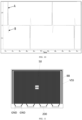
- FIG. 10 is a simulation of coupling noise between a cathode and a touch structure in each of a touch display panel shown in FIG. 1 and a touch display panel shown in FIG. 5 according to an embodiment of the present disclosure.
- a curve A represents the coupling noise between the cathode and the touch structure in the touch display panel shown in FIG. 1
- a curve B represents the coupling noise between the cathode and the touch structure in the touch display panel shown in FIG. 5 . It can be seen that in the embodiment of the present disclosure, as shown in FIG.
- the shielding layer 50 by providing the shielding layer 50, the fluctuation of the voltage of the cathode caused by jumping of the signals (such as Data) can be effectively shielded, 50% of the noise can be effectively reduced, the signal quantity of the touch signal can be relatively increased, the signal-to-noise ratio can be increased, and the touch performance of the touch screen with the active stylus can be improved.
- the signals such as Data
- an embodiment of the present disclosure further provides a touch display panel, as shown in FIG. 5 and 7 , including following components.
- the display signal lines 20 include a first signal line (201, 202, 203, 202') and a second signal line (VDD, VSS, Vinit), the first signal line (201, 202, 203, 202') is configured to input an alternating current signal, the second signal line (VDD, VSS, Vinit) is configured to input a direct current signal;
- An overlapping area between the orthographic projection of the shielding layer 50 on the base substrate 10 and an orthographic projection of the first signal line (201, 202, 203, 202') on the base substrate 10 is greater than an overlapping area between the orthographic projection of the shielding layer 50 on the base substrate 10 and an orthographic projection of the second signal line (VDD, VSS, Vinit) on the base substrate 10.
- the shielding layer covering at least part of the display signal lines is provided between the display signal lines and the touch structure, so that the interference of the signal jumps of the display signal lines (loaded with alternating current signals) to the cathode in the light-emitting devices can be effectively shielded, and the stability of the voltage of the cathode can be ensured, thereby reducing coupling noise between the cathode and the driving electrodes and the sensing electrodes, and improving the signal-to-noise ratio of the touch display panel.
- FIG. 5 shows that the shielding layer 50 is disposed between the display signal lines 20 and the light-emitting devices 30, which is not limited thereto.
- the shielding layer 50 is disposed between the light-emitting devices 30 and the touch structure 40, so that even if the voltage of the cathode is unstable, the driving electrodes and the sensing electrodes in the touch structure 30 are not affected.
- the first signal line may include at least one of the data signal lines 203, the scanning signal lines 202, the reset signal lines 202' and the light-emitting control signal lines 201
- the second signal line includes at least one of the high voltage power lines VDD, the low voltage power line VSS and the initialization signal line Vinit.
- the first signal line preferably includes the data signal lines 203, the scanning signal lines 202, the reset signal lines 202', and the light-emitting control signal lines 201, so that the interference of all the display signal lines loaded with the alternating current signals to the cathode can be effectively avoided, the stability of the voltage of the cathode can be further improved, and the coupling noise between the cathode and the driving electrodes and the sensing electrodes can be minimized.
- the embodiment of the present disclosure further provides a display apparatus, which includes the touch display panel provided by the embodiment of the present disclosure. Since the principle of the display apparatus for solving the problems is similar to that of the touch display panel, the implementation of the display apparatus may be referred to the implementation of the touch display panel, and repeated descriptions are omitted.
- the display apparatus may be: any product or component with a display function, such as a mobile phone, a tablet computer, a television, a display, a notebook computer, a digital photo frame, or a navigator or the like.
- the implementation of the display apparatus may be referred to the embodiments of the touch display panel, and repeated descriptions are omitted.
- the display apparatus provided by the embodiment of the present disclosure further includes a flexible circuit board 200, the flexible circuit board 20 includes a ground pad (GND) and a constant voltage pad (not shown), and the shield layer 50 may be electrically connected to at least two ground pads (GND) or at least two constant voltage pads, or at least one ground pad (GND) and at least one constant voltage pad.
- the shield layer 50 may be ensured to be electrically connected to at least one other ground pad or constant voltage pad in the event that one of the ground pads or constant voltage pads fails.
- the display apparatus provided in the embodiment of the present disclosure further includes an active stylus.
- the shielding layer is disposed between the display signal lines and the light-emitting devices in the embodiment of the present disclosure, so that the voltage fluctuation caused by the signal jumps of the data signal lines and the like can be effectively shielded, the stability of the voltage of the cathode can be ensured, the coupling noise between the cathode and the driving electrodes and the sensing electrodes in the touch structure can be reduced, the signal-to-noise ratio of the touch display panel can be improved, and a major problem in the large-sized OLED display panel can be solved that the active stylus cannot implement the touch function, thereby improving the core competitiveness of the large-sized OLED display product.
- the embodiment of the present disclosure provides a touch display panel and a display apparatus.
- the shielding layer covering the plurality of display signal lines is provided between the plurality of display signal lines and the plurality of light-emitting devices, so that the interference caused by the signal jumps of the display signal lines to the cathode in the light-emitting devices can be effectively shielded, the stability of the voltage of the cathode can be ensured, the coupling noise between the cathode and the driving electrodes and the sensing electrodes can be reduced, and the signal-to-noise ratio of the touch display panel can be improved.
Landscapes
- Engineering & Computer Science (AREA)
- General Engineering & Computer Science (AREA)
- Theoretical Computer Science (AREA)
- Human Computer Interaction (AREA)
- Physics & Mathematics (AREA)
- General Physics & Mathematics (AREA)
- Microelectronics & Electronic Packaging (AREA)
- Computer Networks & Wireless Communication (AREA)
- Electroluminescent Light Sources (AREA)
- Devices For Indicating Variable Information By Combining Individual Elements (AREA)
- Position Input By Displaying (AREA)
Abstract
Description
- The present disclosure relates to the field of touch display technology, and in particular to a touch display panel and a display apparatus.
- With the continuous development of electronic products, an AMOLED (Active Matrix Organic Light-Emitting Diode) display apparatus may realize a full screen, a narrow bezel, a high resolution, rollable wearing, folding, and the like, and therefore, is widely applied. The technology of directly forming a touch structure (Flexible Multi-Layer On Cell, FMLOC) on an encapsulation layer of an OLED (Organic Light-Emitting Diode) touch display panel may form a lighter and thinner display apparatus, and may be applied to a folded and rollable OLED display apparatus.
- Embodiments of the present disclosure provide a touch display panel and a display apparatus, and the specific solutions are as follows.
- The embodiments of the present disclosure provide a touch display panel, including: a base substrate; a plurality of display signal lines on one side of the base substrate; a plurality of light-emitting devices in an array on a side of the plurality of display signal lines away from the base substrate; a touch structure on a side of the plurality of light-emitting devices away from the base substrate; and a shielding layer between the plurality of display signal lines and the plurality of light-emitting devices, an orthographic projection of the shielding layer on the base substrate covers at least a part of an orthographic projection of the plurality of display signal lines on the base substrate.
- In some implementations, in the touch display panel provided by the embodiments of the present disclosure, an orthographic projection of the plurality of display signal lines on the base substrate is within the orthographic projection of the shielding layer on the base substrate.
- In some implementations, in the touch display panel provided by the embodiments of the present disclosure, the shielding layer is made of a conductive material, and is loaded with a constant voltage signal or is grounded.
- In some implementations, in the touch display panel provided by the embodiments of the present disclosure, the shielding layer is made of Ti/Al/Ti, Cu or ITO.
- In some implementations, in the touch display panel provided by the embodiment of the present disclosure, the touch display panel includes a display region and a frame region around the display region; the touch display panel further includes: a high voltage power line in the display region and extending to the frame region, and a low voltage power line in the frame region; and the touch display panel further includes a first conductive connection part and a second conductive connection part independent from each other in the frame region and in the same layer as the shielding layer; the first conductive connection part is electrically connected to the high voltage power line, and the second conductive connection part is electrically connected to the low voltage power line.
- In some implementations, in the touch display panel provided by the embodiments of the present disclosure, the shielding layer has a mesh structure.
- In some implementations, in the touch display panel provided by the embodiments of the present disclosure, the plurality of display signal lines include at least one of a data signal line, a scanning signal line, a reset signal line, and a light-emitting control signal line.
- In some implementations, in the touch display panel provided by the embodiments of the present disclosure, the touch display panel further includes a gate electrode in the same layer as the light-emitting control signal line, and the orthographic projection of the shielding layer on the base substrate further covers an orthographic projection of the gate electrode on the base substrate.
- In some implementations, in the touch display panel provided by the embodiments of the present disclosure, the data signal line is between the base substrate and the shielding layer, the scanning signal line and the reset signal line are in the same layer and located between the data signal line and the base substrate, and the light-emitting control signal line is between the scanning signal line and the base substrate.
- In some implementations, in the touch display panel provided by the embodiments of the present disclosure, the touch display panel further includes: a first planarization layer between the data signal line and the scanning signal line, a second planarization layer between the data signal line and the shielding layer, and a third planarization layer between the shielding layer and the plurality of light-emitting devices; and a shape of the third planarization layer is the same as that of the second planarization layer.
- In some implementations, in the touch display panel provided by the embodiments of the present disclosure, the touch display panel further includes: an encapsulation layer between the plurality of light-emitting devices and the touch structure, a polarizer on a side of the touch structure away from the base substrate, an optical adhesive on a side of the polarizer away from the base substrate, and a cover plate on a side of the optical adhesive away from the base substrate.
- Accordingly, embodiments of the present disclosure further provide a touch display panel, including: a base substrate; a plurality of display signal lines on one side of the base substrate; a plurality of light-emitting devices in an array on a side of the plurality of display signal lines away from the base substrate; an encapsulation layer on a side of the plurality of light-emitting devices away from the base substrate; a touch structure on a side of the encapsulation layer away from the base substrate; and a shielding layer between the plurality of display signal lines and the touch structure, and an orthographic projection of the shielding layer on the base substrate covers at least a part of an orthographic projection of the plurality of display signal lines on the base substrate; the plurality of display signal lines include a first signal line and a second signal line, the first signal line is configured to input an alternating current signal, and the second signal line is configured to input a direct current signal; and an overlapping area between the orthographic projection of the shielding layer on the base substrate and an orthographic projection of the first signal line on the base substrate is greater than an overlapping area between the orthographic projection of the shielding layer on the base substrate and an orthographic projection of the second signal line on the base substrate.
- In some implementations, in the touch display panel provided by the embodiment of the present disclosure, the first signal line includes at least one of a data signal line, a scanning signal line, a reset signal line, and a light-emitting control signal line, and the second signal line includes at least one of a high voltage power line, a low voltage power line, and an initialization signal line.
- Embodiments of the present disclosure further provide a display apparatus, which includes the touch display panel provided by the embodiments of the present disclosure.
- In some implementations, in the display apparatus provided by the embodiments of the present disclosure, the display apparatus further includes a flexible circuit board, the flexible circuit board includes at least one ground pad and at least one constant voltage pad, and the shield layer is at least electrically connected to two ground pads, or two constant voltage pads, or one ground pad and one constant voltage pad.
- In some implementations, in the display apparatus provided by the embodiments of the present disclosure, the display apparatus further includes an active stylus.
-
-
FIG. 1 is a schematic diagram of a structure of a touch screen in the related art; -
FIG. 2 is a schematic diagram of a coupling noise model corresponding to a display module shown inFIG. 1 ; -
FIG. 3 is a schematic diagram showing signal waveforms of data signal lines, a cathode and the like; -
FIG. 4 is a schematic diagram showing influence of a signal jump of a data signal line on a voltage of a cathode; -
FIG. 5 is a schematic cross-sectional view of a touch display panel according to an embodiment of the present disclosure; -
FIG. 6 is a schematic plan view of a touch display panel without a shielding layer according to an embodiment of the present disclosure; -
FIG. 7 is a schematic plan view of a touch display panel with a shielding layer according to an embodiment of the present disclosure; -
FIG. 8 is a schematic plan view of a touch display panel according to an embodiment of the present disclosure; -
FIGS. 9A to 9H are schematic plan views of layers shown inFIG. 7 ; -
FIG. 10 is a schematic diagram illustrating simulation of coupling noise between a cathode and a touch structure in each of a touch display panel shown inFIG. 1 and a touch display panel shown inFIG. 5 according to an embodiment of the present disclosure; and -
FIG. 11 is a schematic plan view of a display apparatus according to an embodiment of the present disclosure. - To make the objects, technical solutions and advantages of the embodiments of the present disclosure more apparent, the technical solutions of the embodiments of the present disclosure will be clearly and completely described below with reference to the drawings of the embodiments of the present disclosure. It is to be understood that the described embodiments are only a few, not all of, embodiments of the present disclosure. The embodiments and features of the embodiments in the present disclosure may be combined with each other without conflict. All other embodiments, which can be derived by a person skilled in the art from the embodiments of the present disclosure without any creative effort, are within the protection scope of the present disclosure.
- Unless defined otherwise, technical or scientific terms used herein shall have the ordinary meaning as understood by one of ordinary skill in the art to which the present disclosure belongs. The term "comprising", "including", or the like means that the element or item preceding the term contains the element or item listed after the term and its equivalent, but does not exclude other elements or items. The term "connected", "coupled", or the like is not limited to physical or mechanical connections, but may include electrical connections, whether direct or indirect connections. The terms "inner", "outer", "upper", "lower", and the like are used only for indicating relative positional relationships, and when the absolute position of an object being described is changed, the relative positional relationships may also be changed accordingly.
- It should be noted that the sizes and shapes of various elements shown in the drawings are not necessarily drawn to scale and are merely schematic representations of the present disclosure. Like or similar elements or elements having like or similar functions are denoted by like or similar reference signs throughout the various figures.
- A capacitive touch screen on the market today has a touch function with a stylus, in addition to the common touch function with a finger. The stylus may include a passive stylus or an active stylus. The active stylus has a small and exquisite pen point and has the functions such as pen pressure, suspension touch, button and the like, and thus has a wider application scene and prospect than the passive stylus. With the popularization of the active stylus, more and more touch screens, for example an electronic product with a touch screen, such as a mobile phone, a notebook computer, or a tablet computer, or the like, are equipped with the active stylus, which has higher requirements on various performances of the active stylus. Thus, the characteristics of the active stylus, including accuracy, a signal-to-noise ratio (SNR), and a hover height, need to be improved.
- With the demand of a terminal customer for the product to be light, thin, folded and rollable, the conventional external hanging touch screen cannot be matched with the OLED, so the FMLOC touch technology is emerged. As shown in
FIG. 1 , the touch screen includes adisplay panel 1, anencapsulation layer 2, atouch structure 3, a polarizer 4, an optical adhesive 5 and acover plate 6, which are sequentially stacked. That is, thetouch structure 3 is directly formed on theencapsulation layer 2 on thedisplay panel 1, and may adopt a metal mesh structure. That is, driving electrodes Tx and sensing electrodes Rx are located in the same layer, and are cooperated with a touch IC to realize the touch function. - As shown in
FIG. 1 , thedisplay panel 1 includes abase substrate 11, anactive layer 12, agate insulating layer 13, afirst gate layer 14, afirst insulating layer 15, asecond gate layer 16, aninterlayer insulating layer 17, a first source-drain metal layer 18, afirst planarization layer 19, a second source-drain metal layer 21 (provided with signal lines such as data signal lines therein), asecond planarization layer 22, and a plurality of light-emitting devices, which are sequentially stacked. Each light-emitting device includes ananode 231, aluminescent layer 232, and acathode 233, which are sequentially arranged, and thecathode 233 is closer to theencapsulation layer 2. As shown inFIG. 1 , compared to the external hanging touch screen, the FMLOC touch screen is integrated on theencapsulation layer 2 on thedisplay panel 1, Tx channels and Rx channels are closer to the cathode of thedisplay panel 1, as shown inFIGS. 2 and 3. FIG. 2 is a schematic diagram of a coupling noise model corresponding to a display module shown inFIG. 1 . A data driving chip (S-IC) is used to load the data signal lines (S1, S2, S3 ...... Sn) with data signals, a parasitic capacitor Cp exists between each of the data signal lines (S1, S2, S3 ...... Sn) and thecathode 233, and a coupling capacitor (Ctx or Crx) exists between thecathode 233 and each of the driving electrodes Tx and the sensing electrodes Rx.FIG. 3 is a schematic diagram showing signal waveforms of data signal lines (S1, S2, S3 ...... Sn), acathode 233 and the like. As may be seen fromFIG. 3 , data signal jumps (including jumps from high to low, and from low to high) may be generated during the row refresh, and data signals in the data signal lines (S1, S2, S3 ...... Sn) generate a large voltage fluctuation (ripple) at the data signal jumps, which disturbs the stability of the voltage of thecathode 233, so that the coupling noise of thecathode 233 to the driving electrodes Tx and the sensing electrodes Rx of thetouch structure 3 inFIG. 2 has a large fluctuation. As shown inFIG. 4 , the Data jump inFIG. 4 means that (a spike of) the coupling noise between thecathode 233 and the driving electrodes Tx and the sensing electrodes Rx is large due to the large voltage fluctuation generated at the data signal jumps. When a magnitude of the coupling noise reaches a certain degree, the SNR of the touch screen is seriously low, the touch chip (T-IC) cannot distinguish the coupling noise from the touch signal quantity, and thus the touch function cannot be realized. Especially in the aspect of the active stylus function, the active stylus point is small (about 1 mm), the coupling signal quantity between the active stylus point and the driving electrodes Tx and the sensing electrodes Rx is very small, and the active stylus has a synchronization function with the smaller signal quantity in a Hover state besides the conventional writing in a contact mode, so if the coupling noise is large, the active stylus function cannot be realized in the large-sized OLED. - Therefore, how to reduce the coupling noise between the cathode and the driving electrodes Tx and the sensing electrodes Rx caused by the data signal jumps becomes a key for solving the problem of the active stylus in the large-sized OLED.
- In view of the above, in order to reduce coupling noise between the cathode and the driving electrodes Tx and the sensing electrodes Rx caused by the data signal jumps, an embodiment of the present disclosure provides a touch display panel, as shown in
FIGS. 5 to 7 .FIG. 5 is a schematic cross-sectional view of a touch display panel;FIG. 6 is a schematic plan view of a touch display panel without a shielding layer;FIG. 7 is a schematic plan view of a touch display panel with a shielding layer.FIG. 5 is a schematic cross-sectional view of the touch display panel along a CC' line inFIG. 7 . The touch display panel includes following components: - A
base substrate 10; - A plurality of
display signal lines 20 disposed on one side of thebase substrate 10; - A plurality of light-emitting
devices 30 arranged in an array on a side of the plurality ofdisplay signal lines 20 away from thebase substrate 10; - A
touch structure 40 disposed on a side of the plurality of light-emittingdevices 30 away from thebase substrate 10; - A
shielding layer 50 disposed between the plurality ofdisplay signal lines 20 and the plurality of light-emittingdevices 30, wherein an orthographic projection of theshielding layer 50 on thebase substrate 10 covers at least a part of an orthographic projection of the plurality ofdisplay signal lines 20 on thebase substrate 10. - Optionally, as shown in
FIG. 5 to FIG. 7 , thedisplay signal lines 20 may include at least one of data signal lines 203 (Data), scanning signal lines 202 (Gate), reset signal lines 202' (Reset), and light-emitting control signal lines 201 (EM), where signals loaded on these signal lines are all alternating current signals (i.e., signals jumping from high to low and from low to high). The jumping signals may cause large voltage fluctuation, so that a voltage of the cathode (which will be described below) of the light-emittingdevice 30 is unstable. Specifically, each data signalline 203 is configured to provide a display data signal for the touch display panel, eachscanning signal line 202 is configured to provide a display driving signal for the touch display panel, each reset signal line 202' is configured to provide a reset signal for the touch display panel, and each light-emittingcontrol signal line 201 is configured to provide a light-emitting control signal for the touch display panel. - In particular, as shown in
FIG. 5 , the light-emittingdevices 30 may include a red (R) light-emitting device, a green (G) light-emitting device, and a blue (B) light-emitting device. Each light-emittingdevice 30 includes ananode 301, aluminescent layer 302, and acathode 303, which are sequentially stacked. Theanodes 301 of all the light-emittingdevices 30 may be arranged independently of each other, and all the light-emittingdevices 30 may share one cathode 303 (i.e., the cathode is arranged on an entire surface). Thetouch structure 40 may include driving electrodes Tx and sensing electrodes Rx, which are insulated from each other and arranged in a crossing manner and in the same layer. - In specific implementation, in the touch display panel provided in the embodiment of the present disclosure, as shown in
FIG. 5 andFIG. 7 , theshielding layer 50 may be made of a conductive material. For example, the material of the shielding layer may be, but is not limited to, Ti/Al/Ti, Cu, ITO, or the like. Alternatively, a sheet resistance of the conductive material used to form the shielding layer should be as low as possible. - In some embodiments, as shown in
FIGS. 5 and7 , theshielding layer 50 may be loaded with a constant voltage signal or be grounded. When theshielding layer 50 is loaded with a constant voltage signal or is grounded, the interference of the signal jumps of thedisplay signal lines 20 to thecathode 303 in the light-emittingdevices 30 can be effectively shielded, and the stability of the voltage of thecathode 303 can be ensured, so that the coupling noise between thecathode 303 and the driving electrodes Tx and the sensing electrodes Rx in thetouch structure 40 can be reduced. - According to the touch display panel provided by the embodiment of the present disclosure, the
shielding layer 50 covering thedisplay signal lines 20 is provided between thedisplay signal lines 20 and the light-emittingdevices 30, so that the interference of the signal jumps of thedisplay signal lines 20 to thecathode 303 in the light-emittingdevices 30 can be effectively shielded, and the stability of the voltage of the cathode can be ensured, so that the coupling noise between the cathode and the driving electrodes Tx and the sensing electrodes Rx can be reduced and the signal-to-noise ratio of the touch display panel is improved. - Specifically, as shown in
FIG. 5 andFIG. 7 , in the embodiment of the present disclosure, preferably, an orthographic projection of theshielding layer 50 on thebase substrate 10 covers an orthographic projection of each of the data signalline 203, thescanning signal line 202, the reset signal line 202', and the light-emittingcontrol signal line 201 on thebase substrate 10, so that the interference of all signal lines loaded with the alternating current signals to the cathode can be effectively avoided, the stability of the voltage of the cathode can be further improved, and the coupling noise between the cathode and the driving electrodes and the sensing electrodes can be minimized. - In specific implementation, in the touch display panel provided by the embodiment of the present disclosure, as shown in
FIG. 5 andFIG. 7 , an orthographic projection of the plurality of display signal lines 20 (the data signallines 203, thescanning signal lines 202, the reset signal lines 202', and the light-emitting control signal lines 201) on thebase substrate 10 is located within the orthographic projection of theshielding layer 50 on thebase substrate 10. Thus, the interference of the jumping signals (alternating current signals) on the data signallines 203, thescanning signal lines 202, the reset signal lines 202', and the light-emittingcontrol signal lines 201 to the cathode can be completely shielded by theshielding layer 50. - In specific implementation, as shown in
FIGS. 5 to 7 , in the touch display panel provided in the embodiment of the present disclosure, the data signallines 203 are located between thebase substrate 10 and theshielding layer 50, thescanning signal lines 202 and the reset signal lines 202' are disposed in the same layer and located between the data signallines 203 and thebase substrate 10, and the light-emittingcontrol signal lines 201 are located between thescanning signal lines 202 and thebase substrate 10. Specifically, a layer where the light-emittingcontrol signal lines 201 are located is a first gate metal layer (Gatel), a layer where thescanning signal lines 202 and the reset signal lines 202' are located is a first source drain metal layer (SD1), and a layer where the data signallines 203 are located is a second source drain metal layer (SD2). - In specific implementation, as shown in
FIGS. 5 to 7 , the touch display panel provided in the embodiment of the present disclosure further includes: afirst planarization layer 61 located between the data signallines 203 and thescanning signal lines 202, asecond planarization layer 62 located between the data signallines 203 and theshield layer 50, and athird planarization layer 63 located between theshield layer 50 and the light-emittingdevices 30. A shape of thethird planarization layer 63 is the same as that of thesecond planarization layer 62. Optionally, a material and a thickness of thethird planarization layer 63 may or may not be the same as those of thesecond planarization layer 62. - In specific implementation, as shown in
FIGS. 5 to 7 , the touch display panel provided in the embodiment of the present disclosure further includes: a second gate metal layer 60 (Gate2) located between the light-emittingcontrol signal lines 201 and the scanning signal lines 202. The secondgate metal layer 60 is used for forming one plate of a storage capacitor in each pixel circuit of the display panel. - In specific implementation, as shown in
FIGS. 5 to 7 , the touch display panel provided in the embodiment of the present disclosure further includes: afourth planarization layer 64 located between the light-emittingcontrol signal lines 201 and the secondgate metal layer 60, aninterlayer insulating layer 65 located between the secondgate metal layer 60 and thescanning signal lines 202, anactive layer 70 located between thebase substrate 10 and the light-emittingcontrol signal lines 201, and agate insulating layer 80 located between theactive layer 70 and the light-emitting control signal lines 201. - In specific implementation, as shown in
FIG. 5 , the touch display panel provided in the embodiment of the present disclosure further includes: anencapsulation layer 90 located between the light-emittingdevices 30 and thetouch structure 40, apolarizer 100 located on a side of thetouch structure 40 away from thebase substrate 10, anoptical adhesive 101 located on a side of thepolarizer 100 away from thebase substrate 10, and acover plate 102 located on a side of theoptical adhesive 101 away from thebase substrate 10. - Specifically, the
encapsulation layer 90 may include a first inorganic layer, an organic layer, and a second inorganic layer stacked together, theoptical adhesive 101 may be an OCA (Optically Clear Adhesive), and the cover plate may be a glass cover plate. - In specific implementation, in the touch display panel provided in the embodiment of the present disclosure, as shown in
FIG. 7 , theshielding layer 50 has a mesh structure. Thus, theshielding layer 50 only covers thedisplay signal lines 20, without affecting an aperture ratio of the touch display panel. - In specific implementation, the scanning signal lines are generally electrically connected to gate driver circuits (gate driver on array, GOAs), and each signal output terminal of each GOA is configured to input a scanning driving signal to each scanning signal line. The scanning signal lines are electrically connected to gate electrodes of thin film transistors in the display panel, so that the stability of the voltage of the cathode is further affected by the signal jumps on the gate electrodes. As shown in
FIG. 4 , the GOA jump refers to that the coupling noise (spike) between a cathode and the driving electrodes Tx and the sensing electrodes Rx is large due to the fluctuation of the voltage of the cathode caused by the jumping of the scanning driving signals. Therefore, in the touch display panel provided in the embodiment of the present disclosure, as shown inFIG. 7 , the touch display panel further includes gate electrodes 201' disposed in the same layer as the light-emittingcontrol signal lines 201, and the orthographic projection of theshielding layer 50 on thebase substrate 10 also covers an orthographic projection of the gate electrodes 201' on thebase substrate 10. Therefore, the interference of the jumping signals on the gate electrodes 201' to the cathode in the light-emittingdevices 30 can be shielded by theshielding layer 50, and the stability of the voltage of the cathode can be further ensured. - In a specific implementation, as shown in
FIG. 8 , in the touch display panel provided in the embodiment of the present disclosure, the touch display panel has a display region AA and a frame region BB disposed around the display region AA. The touch display panel further includes: a high voltage power line VDD located in the display region AA and extending to the frame region BB, and a low voltage power line VSS located in the frame region BB. The low voltage power line VSS is generally disposed around the display region AA, and the low voltage power line VSS and the high voltage power line VDD are generally disposed in the same layer as the data signalline 203. In order to reduce resistances of the low voltage power line VSS and the high voltage power line VDD, the touch display panel further includes a firstconductive connection part 1011 and a secondconductive connection part 1012 located in the frame region BB independent from each other and in the same layer as theshielding layer 50. The firstconductive connection part 1011 may be electrically connected to the high voltage power line VDD through a first via 621 penetrating through the second planarization layer 62 (not shown), and the secondconductive connection part 1012 is electrically connected to the low voltage power line VSS through a second via 622 penetrating through thesecond planarization layer 62. Therefore, the display uniformity of the large-sized touch display panel can be improved by reducing the resistances of the high voltage power lines VDD or the low voltage power line VSS. - It should be noted that in the embodiment of the present disclosure,
FIG. 8 is only for schematically illustrating an electrical connection relationship between the firstconductive connection part 1011 and the high voltage power lines VDD, and an electrical connection relationship between the secondconductive connection part 1012 and the low voltage power line VSS. Patterns of the firstconductive connection part 1011 electrically connected to the high voltage power lines VDD and the secondconductive connection part 1012 electrically connected to the low voltage power line VSS are designed according to actual structures of the high voltage power line VDD and the low voltage power line VSS. - As shown in
FIGS. 9A to 9H, FIGS. 9A to 9H are schematic diagrams of layout of layers inFIG. 7 .FIG. 9A is a schematic plan diagram of theactive layer 70.FIG. 9B is a schematic plan diagram of the first gate metal layer (Gate1). The first gate metal layer (Gate1) includes the light-emittingcontrol signal line 201, the gate electrodes 201', and theother plate 201" of the storage capacitor in each pixel circuit of the display panel and the like.FIG. 9C is a schematic plan diagram of the second gate metal layer (Gate2).FIG. 9D is a schematic plan diagram ofthird vias 651 in theinterlayer insulating layer 65.FIG. 9E is a schematic plan diagram of the first source drain metal layer (SD1). The first source drain metal layer (SD1) includes thescanning signal lines 202, the reset signal lines 202', and theconductive connection parts 202" electrically connected to the high voltage power lines VDD located in the second source drain metal layer (SD2) for reducing the resistances of the high voltage power lines VDD.FIG. 9F is a schematic plan view offourth vias 611 in thefirst planarization layer 61.FIG. 9G is a schematic plan view of the second source drain metal layer (SD2). The second source drain metal layer (SD2) includes the data signallines 203, the high voltage power lines VDD, initialization signal lines Vinit, and the like.FIG. 9H is a schematic plan view of theshielding layer 50. - As shown in
FIG. 10, FIG. 10 is a simulation of coupling noise between a cathode and a touch structure in each of a touch display panel shown inFIG. 1 and a touch display panel shown inFIG. 5 according to an embodiment of the present disclosure. A curve A represents the coupling noise between the cathode and the touch structure in the touch display panel shown inFIG. 1 , and a curve B represents the coupling noise between the cathode and the touch structure in the touch display panel shown inFIG. 5 . It can be seen that in the embodiment of the present disclosure, as shown inFIG. 5 , by providing theshielding layer 50, the fluctuation of the voltage of the cathode caused by jumping of the signals (such as Data) can be effectively shielded, 50% of the noise can be effectively reduced, the signal quantity of the touch signal can be relatively increased, the signal-to-noise ratio can be increased, and the touch performance of the touch screen with the active stylus can be improved. - Based on the same inventive concept, an embodiment of the present disclosure further provides a touch display panel, as shown in
FIG. 5 and7 , including following components. - A
base substrate 10; - A plurality of
display signal lines 20 disposed on one side of thebase substrate 10; - A plurality of light-emitting
devices 30 arranged in an array on a side of the plurality ofdisplay signal lines 20 away from thebase substrate 10; - An
encapsulation layer 90 disposed on a side of the plurality of light-emittingdevices 30 away from thebase substrate 10; - A
touch structure 40 disposed on a side of theencapsulation layer 90 away from thebase substrate 10; - A
shielding layer 50 disposed between the plurality ofdisplay signal lines 20 and thetouch structure 40, wherein an orthographic projection of theshielding layer 50 on thebase substrate 10 covers at least a part of an orthographic projection of the plurality ofdisplay signal lines 20 on thebase substrate 10. - The
display signal lines 20 include a first signal line (201, 202, 203, 202') and a second signal line (VDD, VSS, Vinit), the first signal line (201, 202, 203, 202') is configured to input an alternating current signal, the second signal line (VDD, VSS, Vinit) is configured to input a direct current signal;
An overlapping area between the orthographic projection of theshielding layer 50 on thebase substrate 10 and an orthographic projection of the first signal line (201, 202, 203, 202') on thebase substrate 10 is greater than an overlapping area between the orthographic projection of theshielding layer 50 on thebase substrate 10 and an orthographic projection of the second signal line (VDD, VSS, Vinit) on thebase substrate 10. - According to the touch display panel provided by the embodiment of the present disclosure, the shielding layer covering at least part of the display signal lines is provided between the display signal lines and the touch structure, so that the interference of the signal jumps of the display signal lines (loaded with alternating current signals) to the cathode in the light-emitting devices can be effectively shielded, and the stability of the voltage of the cathode can be ensured, thereby reducing coupling noise between the cathode and the driving electrodes and the sensing electrodes, and improving the signal-to-noise ratio of the touch display panel.
- It should be noted that in the embodiment of the present disclosure,
FIG. 5 shows that theshielding layer 50 is disposed between thedisplay signal lines 20 and the light-emittingdevices 30, which is not limited thereto. For example, theshielding layer 50 is disposed between the light-emittingdevices 30 and thetouch structure 40, so that even if the voltage of the cathode is unstable, the driving electrodes and the sensing electrodes in thetouch structure 30 are not affected. - In an implementation, in the touch display panel provided by the embodiment of the present disclosure, the first signal line may include at least one of the data signal
lines 203, thescanning signal lines 202, the reset signal lines 202' and the light-emittingcontrol signal lines 201, and the second signal line includes at least one of the high voltage power lines VDD, the low voltage power line VSS and the initialization signal line Vinit. Specifically, in the embodiment of the present disclosure, the first signal line preferably includes the data signallines 203, thescanning signal lines 202, the reset signal lines 202', and the light-emittingcontrol signal lines 201, so that the interference of all the display signal lines loaded with the alternating current signals to the cathode can be effectively avoided, the stability of the voltage of the cathode can be further improved, and the coupling noise between the cathode and the driving electrodes and the sensing electrodes can be minimized. - Based on the same inventive concept, the embodiment of the present disclosure further provides a display apparatus, which includes the touch display panel provided by the embodiment of the present disclosure. Since the principle of the display apparatus for solving the problems is similar to that of the touch display panel, the implementation of the display apparatus may be referred to the implementation of the touch display panel, and repeated descriptions are omitted. The display apparatus may be: any product or component with a display function, such as a mobile phone, a tablet computer, a television, a display, a notebook computer, a digital photo frame, or a navigator or the like. The implementation of the display apparatus may be referred to the embodiments of the touch display panel, and repeated descriptions are omitted.
- In specific implementation, as shown in
FIG. 11 , the display apparatus provided by the embodiment of the present disclosure further includes a flexible circuit board 200, theflexible circuit board 20 includes a ground pad (GND) and a constant voltage pad (not shown), and theshield layer 50 may be electrically connected to at least two ground pads (GND) or at least two constant voltage pads, or at least one ground pad (GND) and at least one constant voltage pad. In this way, theshield layer 50 may be ensured to be electrically connected to at least one other ground pad or constant voltage pad in the event that one of the ground pads or constant voltage pads fails. - In specific implementation, the display apparatus provided in the embodiment of the present disclosure further includes an active stylus. The shielding layer is disposed between the display signal lines and the light-emitting devices in the embodiment of the present disclosure, so that the voltage fluctuation caused by the signal jumps of the data signal lines and the like can be effectively shielded, the stability of the voltage of the cathode can be ensured, the coupling noise between the cathode and the driving electrodes and the sensing electrodes in the touch structure can be reduced, the signal-to-noise ratio of the touch display panel can be improved, and a major problem in the large-sized OLED display panel can be solved that the active stylus cannot implement the touch function, thereby improving the core competitiveness of the large-sized OLED display product.
- The embodiment of the present disclosure provides a touch display panel and a display apparatus. The shielding layer covering the plurality of display signal lines is provided between the plurality of display signal lines and the plurality of light-emitting devices, so that the interference caused by the signal jumps of the display signal lines to the cathode in the light-emitting devices can be effectively shielded, the stability of the voltage of the cathode can be ensured, the coupling noise between the cathode and the driving electrodes and the sensing electrodes can be reduced, and the signal-to-noise ratio of the touch display panel can be improved.
- While preferred embodiments of the present disclosure have been described, additional variations and modifications in these embodiments may occur to one of ordinary skill in the art once they learn of the basic inventive concepts. Therefore, it is intended that the appended claims are interpreted as including the preferred embodiments and all variations and modifications that fall within the scope of the present disclosure.
- It will be apparent to one of ordinary skill in the art that various changes and modifications may be made in the embodiments of the present disclosure without departing from the spirit and scope of the present disclosure. Thus, if these modifications and variations of the embodiments of the present disclosure fall within the scope of the claims of the present disclosure and their equivalents, the present disclosure is also intended to include such modifications and variations.
Claims (16)
- A touch display panel, comprising:a base substrate;a plurality of display signal lines on one side of the base substrate;a plurality of light-emitting devices arranged in an array on a side of the plurality of display signal lines away from the base substrate;a touch structure on a side of the plurality of light-emitting devices away from the base substrate; anda shielding layer between the plurality of display signal lines and the plurality of light-emitting devices, wherein an orthographic projection of the shielding layer on the base substrate covers at least a part of an orthographic projection of the plurality of display signal lines on the base substrate.
- The touch display panel of claim 1, wherein an orthographic projection of the plurality of display signal lines on the base substrate is within the orthographic projection of the shielding layer on the base substrate.
- The touch display panel of claim 1, wherein the shielding layer is made of a conductive material, and is loaded with a constant voltage signal or is grounded.
- The touch display panel of claim 3, wherein the shielding layer is made of Ti/Al/Ti, Cu or ITO.
- The touch display panel of any one of claims 1 to 4, wherein the touch display panel comprises a display region and a frame region around the display region; the touch display panel further comprises: a high voltage power line in the display region and extending to the frame region, and a low voltage power line in the frame region; and
the touch display panel further comprises a first conductive connection part and a second conductive connection part arranged independent from each other in the frame region and in a same layer as the shielding layer; the first conductive connection part is electrically connected to the high voltage power line, and the second conductive connection part is electrically connected to the low voltage power line. - The touch display panel of any one of claims 1 to 4, wherein the shielding layer has a mesh structure.
- The touch display panel of any one of claims 1 to 6, wherein the plurality of display signal lines comprise at least one of a data signal line, a scanning signal line, a reset signal line, and a light-emitting control signal line.
- The touch display panel of claim 7, further comprising a gate electrode in a same layer as the light-emitting control signal line,
wherein the orthographic projection of the shielding layer on the base substrate further covers an orthographic projection of the gate electrode on the base substrate. - The touch display panel of claim 7, wherein the data signal line is between the base substrate and the shielding layer, the scanning signal line and the reset signal line are in a same layer and located between the data signal line and the base substrate, and the light-emitting control signal line is between the scanning signal line and the base substrate.
- The touch display panel of claim 9, further comprising: a first planarization layer between the data signal line and the scanning signal line, a second planarization layer between the data signal line and the shielding layer, and a third planarization layer between the shielding layer and the plurality of light-emitting devices.
- The touch display panel of claim 10, further comprising: an encapsulation layer between the plurality of light-emitting devices and the touch structure, a polarizer on a side of the touch structure away from the base substrate, an optical adhesive on a side of the polarizer away from the base substrate, and a cover plate on a side of the optical adhesive away from the base substrate.
- A touch display panel, comprising:a base substrate;a plurality of display signal lines on one side of the base substrate;a plurality of light-emitting devices arranged in an array on a side of the plurality of display signal lines away from the base substrate;an encapsulation layer on a side of the plurality of light-emitting devices away from the base substrate;a touch structure on a side of the encapsulation layer away from the base substrate; anda shielding layer between the plurality of display signal lines and the touch structure, wherein an orthographic projection of the shielding layer on the base substrate covers at least a part of an orthographic projection of the plurality of display signal lines on the base substrate; whereinthe plurality of display signal lines comprise a first signal line and a second signal line, the first signal line is configured to input an alternating current signal, and the second signal line is configured to input a direct current signal; andan overlapping area between the orthographic projection of the shielding layer on the base substrate and an orthographic projection of the first signal line on the base substrate is greater than an overlapping area between the orthographic projection of the shielding layer on the base substrate and an orthographic projection of the second signal line on the base substrate.
- The touch display panel of claim 12, wherein the first signal line comprises at least one of a data signal line, a scanning signal line, a reset signal line, and a light-emitting control signal line, and the second signal line comprises at least one of a high voltage power line, a low voltage power line, and an initialization signal line.
- A display apparatus, comprising the touch display panel of any one of claims 1 to 13.
- The display apparatus of claim 14, further comprising a flexible circuit board, wherein the flexible circuit board comprises at least one ground pad and at least one constant voltage pad, and the shield layer is at least electrically connected to two ground pads, or two constant voltage pads, or one ground pad and one constant voltage pad.
- The display apparatus of claim 14, further comprising an active stylus.
Applications Claiming Priority (1)
| Application Number | Priority Date | Filing Date | Title |
|---|---|---|---|
| PCT/CN2022/122675 WO2024065411A1 (en) | 2022-09-29 | 2022-09-29 | Touch-control display panel and display apparatus |
Publications (2)
| Publication Number | Publication Date |
|---|---|
| EP4471551A1 true EP4471551A1 (en) | 2024-12-04 |
| EP4471551A4 EP4471551A4 (en) | 2025-04-16 |
Family
ID=90475294
Family Applications (1)
| Application Number | Title | Priority Date | Filing Date |
|---|---|---|---|
| EP22960048.1A Pending EP4471551A4 (en) | 2022-09-29 | 2022-09-29 | TOUCH CONTROLLED DISPLAY SCREEN AND DISPLAY APPARATUS |
Country Status (4)
| Country | Link |
|---|---|
| US (2) | US12474799B2 (en) |
| EP (1) | EP4471551A4 (en) |
| CN (1) | CN118303150A (en) |
| WO (1) | WO2024065411A1 (en) |
Family Cites Families (12)
| Publication number | Priority date | Publication date | Assignee | Title |
|---|---|---|---|---|
| CN118244925A (en) * | 2017-11-01 | 2024-06-25 | 株式会社和冠 | Integrated circuit |
| CN109976056B (en) * | 2019-04-08 | 2023-04-14 | 京东方科技集团股份有限公司 | Array substrate, manufacturing method thereof, display panel and display device |
| EP3992705B1 (en) | 2020-05-29 | 2024-11-06 | BOE Technology Group Co., Ltd. | Display substrate and display device |
| CN114115574A (en) | 2020-08-26 | 2022-03-01 | 深圳市柔宇科技股份有限公司 | Touch display panel and electronic equipment |
| WO2022041237A1 (en) | 2020-08-31 | 2022-03-03 | 京东方科技集团股份有限公司 | Display substrate and production method therefor, and display device |
| JP2022047037A (en) * | 2020-09-11 | 2022-03-24 | 株式会社ジャパンディスプレイ | Display device |
| CN112420799B (en) | 2020-11-20 | 2024-03-05 | 京东方科技集团股份有限公司 | Display substrate, display panel and display device |
| CN113555399B (en) | 2021-07-19 | 2024-03-05 | 京东方科技集团股份有限公司 | Display panel and display device |
| CN113964109B (en) * | 2021-10-19 | 2026-05-29 | 成都京东方光电科技有限公司 | Display substrate, preparation method thereof and display device |
| CN114185454B (en) | 2021-12-13 | 2023-06-27 | 武汉华星光电半导体显示技术有限公司 | Display panel and electronic equipment |
| JP2023165450A (en) * | 2022-05-06 | 2023-11-16 | シャープディスプレイテクノロジー株式会社 | Display device and display device manufacturing method |
| GB2620013B (en) * | 2022-05-23 | 2024-09-04 | Lg Display Co Ltd | Touch display device |
-
2022
- 2022-09-29 CN CN202280003382.6A patent/CN118303150A/en active Pending
- 2022-09-29 EP EP22960048.1A patent/EP4471551A4/en active Pending
- 2022-09-29 WO PCT/CN2022/122675 patent/WO2024065411A1/en not_active Ceased
- 2022-09-29 US US18/688,002 patent/US12474799B2/en active Active
-
2025
- 2025-09-19 US US19/334,613 patent/US20260016914A1/en active Pending
Also Published As
| Publication number | Publication date |
|---|---|
| WO2024065411A1 (en) | 2024-04-04 |
| CN118303150A (en) | 2024-07-05 |
| EP4471551A4 (en) | 2025-04-16 |
| US20260016914A1 (en) | 2026-01-15 |
| US12474799B2 (en) | 2025-11-18 |
| US20250123703A1 (en) | 2025-04-17 |
Similar Documents
| Publication | Publication Date | Title |
|---|---|---|
| US11615719B2 (en) | Display panel and display device | |
| US20250081797A1 (en) | Array substrate and display device | |
| US20250028406A1 (en) | Display panel, methods for driving and manufacturing the same, and display apparatus | |
| KR102917479B1 (en) | Display device | |
| US12041814B2 (en) | Display substrate and display device | |
| KR102709634B1 (en) | Display device | |
| US11839018B2 (en) | Flexible printed circuit board and display touch apparatus | |
| US12111992B2 (en) | Touch panel with chip region having display pins and touch pins, preparation method therefor, and display apparatus | |
| US12175048B2 (en) | Self-capacitance touch panel and touch display panel | |
| EP4206877B1 (en) | Transparent touch display device | |
| US12086352B2 (en) | Transparent touch display device | |
| KR20220152469A (en) | Display device | |
| CN116414248A (en) | Transparent touch display device | |
| US20220066588A1 (en) | Touch display panel and electronic device | |
| US20260016922A1 (en) | Touch substrate, touch display panel and touch display apparatus | |
| US12455647B2 (en) | Touch display device and display panel | |
| US12474799B2 (en) | Touch display panel and display apparatus | |
| KR20150070665A (en) | Circuit Board For Touch Sensor Integrated Circuit | |
| CN117501220B (en) | Touch display panel and touch display device | |
| US11797140B2 (en) | Touch sensing unit and display device including the same | |
| CN117438435A (en) | Display panels and display devices | |
| CN116382503A (en) | Transparent touch display device | |
| GB2620013A (en) | Touch display device | |
| US20250060853A1 (en) | Touch sensor including an insulating layer and display device including the same | |
| US20250271967A1 (en) | Display device and method for driving the same |
Legal Events
| Date | Code | Title | Description |
|---|---|---|---|
| STAA | Information on the status of an ep patent application or granted ep patent |
Free format text: STATUS: THE INTERNATIONAL PUBLICATION HAS BEEN MADE |
|
| PUAI | Public reference made under article 153(3) epc to a published international application that has entered the european phase |
Free format text: ORIGINAL CODE: 0009012 |
|
| STAA | Information on the status of an ep patent application or granted ep patent |
Free format text: STATUS: REQUEST FOR EXAMINATION WAS MADE |
|
| 17P | Request for examination filed |
Effective date: 20240827 |
|
| AK | Designated contracting states |
Kind code of ref document: A1 Designated state(s): AL AT BE BG CH CY CZ DE DK EE ES FI FR GB GR HR HU IE IS IT LI LT LU LV MC MK MT NL NO PL PT RO RS SE SI SK SM TR |
|
| A4 | Supplementary search report drawn up and despatched |
Effective date: 20250314 |
|
| RIC1 | Information provided on ipc code assigned before grant |
Ipc: H10K 59/126 20230101ALI20250310BHEP Ipc: H10K 59/131 20230101ALI20250310BHEP Ipc: H10K 59/40 20230101ALI20250310BHEP Ipc: G06F 3/041 20060101AFI20250310BHEP |
|
| DAV | Request for validation of the european patent (deleted) | ||
| DAX | Request for extension of the european patent (deleted) |