EP4468743A1 - Ultrasonic probe and ultrasonic probe manufacturing method - Google Patents
Ultrasonic probe and ultrasonic probe manufacturing method Download PDFInfo
- Publication number
- EP4468743A1 EP4468743A1 EP23743161.4A EP23743161A EP4468743A1 EP 4468743 A1 EP4468743 A1 EP 4468743A1 EP 23743161 A EP23743161 A EP 23743161A EP 4468743 A1 EP4468743 A1 EP 4468743A1
- Authority
- EP
- European Patent Office
- Prior art keywords
- ultrasonic probe
- piezoelectric
- piezoelectric material
- electrode
- piezoelectric element
- Prior art date
- Legal status (The legal status is an assumption and is not a legal conclusion. Google has not performed a legal analysis and makes no representation as to the accuracy of the status listed.)
- Pending
Links
Images


Classifications
-
- H—ELECTRICITY
- H10—SEMICONDUCTOR DEVICES; ELECTRIC SOLID-STATE DEVICES NOT OTHERWISE PROVIDED FOR
- H10N—ELECTRIC SOLID-STATE DEVICES NOT OTHERWISE PROVIDED FOR
- H10N30/00—Piezoelectric or electrostrictive devices
- H10N30/80—Constructional details
- H10N30/87—Electrodes or interconnections, e.g. leads or terminals
- H10N30/877—Conductive materials
- H10N30/878—Conductive materials the principal material being non-metallic, e.g. oxide or carbon based
-
- A—HUMAN NECESSITIES
- A61—MEDICAL OR VETERINARY SCIENCE; HYGIENE
- A61B—DIAGNOSIS; SURGERY; IDENTIFICATION
- A61B8/00—Diagnosis using ultrasonic, sonic or infrasonic waves
- A61B8/42—Details of probe positioning or probe attachment to the patient
- A61B8/4272—Details of probe positioning or probe attachment to the patient involving the acoustic interface between the transducer and the tissue
- A61B8/4281—Details of probe positioning or probe attachment to the patient involving the acoustic interface between the transducer and the tissue characterised by sound-transmitting media or devices for coupling the transducer to the tissue
-
- A—HUMAN NECESSITIES
- A61—MEDICAL OR VETERINARY SCIENCE; HYGIENE
- A61B—DIAGNOSIS; SURGERY; IDENTIFICATION
- A61B8/00—Diagnosis using ultrasonic, sonic or infrasonic waves
- A61B8/44—Constructional features of the ultrasonic, sonic or infrasonic diagnostic device
- A61B8/4483—Constructional features of the ultrasonic, sonic or infrasonic diagnostic device characterised by features of the ultrasound transducer
-
- B—PERFORMING OPERATIONS; TRANSPORTING
- B06—GENERATING OR TRANSMITTING MECHANICAL VIBRATIONS IN GENERAL
- B06B—METHODS OR APPARATUS FOR GENERATING OR TRANSMITTING MECHANICAL VIBRATIONS OF INFRASONIC, SONIC, OR ULTRASONIC FREQUENCY, e.g. FOR PERFORMING MECHANICAL WORK IN GENERAL
- B06B1/00—Methods or apparatus for generating mechanical vibrations of infrasonic, sonic, or ultrasonic frequency
- B06B1/02—Methods or apparatus for generating mechanical vibrations of infrasonic, sonic, or ultrasonic frequency making use of electrical energy
- B06B1/06—Methods or apparatus for generating mechanical vibrations of infrasonic, sonic, or ultrasonic frequency making use of electrical energy operating with piezoelectric effect or with electrostriction
- B06B1/0607—Methods or apparatus for generating mechanical vibrations of infrasonic, sonic, or ultrasonic frequency making use of electrical energy operating with piezoelectric effect or with electrostriction using multiple elements
-
- B—PERFORMING OPERATIONS; TRANSPORTING
- B06—GENERATING OR TRANSMITTING MECHANICAL VIBRATIONS IN GENERAL
- B06B—METHODS OR APPARATUS FOR GENERATING OR TRANSMITTING MECHANICAL VIBRATIONS OF INFRASONIC, SONIC, OR ULTRASONIC FREQUENCY, e.g. FOR PERFORMING MECHANICAL WORK IN GENERAL
- B06B1/00—Methods or apparatus for generating mechanical vibrations of infrasonic, sonic, or ultrasonic frequency
- B06B1/02—Methods or apparatus for generating mechanical vibrations of infrasonic, sonic, or ultrasonic frequency making use of electrical energy
- B06B1/06—Methods or apparatus for generating mechanical vibrations of infrasonic, sonic, or ultrasonic frequency making use of electrical energy operating with piezoelectric effect or with electrostriction
- B06B1/0607—Methods or apparatus for generating mechanical vibrations of infrasonic, sonic, or ultrasonic frequency making use of electrical energy operating with piezoelectric effect or with electrostriction using multiple elements
- B06B1/0622—Methods or apparatus for generating mechanical vibrations of infrasonic, sonic, or ultrasonic frequency making use of electrical energy operating with piezoelectric effect or with electrostriction using multiple elements on one surface
-
- B—PERFORMING OPERATIONS; TRANSPORTING
- B06—GENERATING OR TRANSMITTING MECHANICAL VIBRATIONS IN GENERAL
- B06B—METHODS OR APPARATUS FOR GENERATING OR TRANSMITTING MECHANICAL VIBRATIONS OF INFRASONIC, SONIC, OR ULTRASONIC FREQUENCY, e.g. FOR PERFORMING MECHANICAL WORK IN GENERAL
- B06B1/00—Methods or apparatus for generating mechanical vibrations of infrasonic, sonic, or ultrasonic frequency
- B06B1/02—Methods or apparatus for generating mechanical vibrations of infrasonic, sonic, or ultrasonic frequency making use of electrical energy
- B06B1/06—Methods or apparatus for generating mechanical vibrations of infrasonic, sonic, or ultrasonic frequency making use of electrical energy operating with piezoelectric effect or with electrostriction
- B06B1/0644—Methods or apparatus for generating mechanical vibrations of infrasonic, sonic, or ultrasonic frequency making use of electrical energy operating with piezoelectric effect or with electrostriction using a single piezoelectric element
- B06B1/0662—Methods or apparatus for generating mechanical vibrations of infrasonic, sonic, or ultrasonic frequency making use of electrical energy operating with piezoelectric effect or with electrostriction using a single piezoelectric element with an electrode on the sensitive surface
-
- G—PHYSICS
- G01—MEASURING; TESTING
- G01N—INVESTIGATING OR ANALYSING MATERIALS BY DETERMINING THEIR CHEMICAL OR PHYSICAL PROPERTIES
- G01N29/00—Investigating or analysing materials by the use of ultrasonic, sonic or infrasonic waves; Visualisation of the interior of objects by transmitting ultrasonic or sonic waves through the object
- G01N29/04—Analysing solids
-
- G—PHYSICS
- G01—MEASURING; TESTING
- G01N—INVESTIGATING OR ANALYSING MATERIALS BY DETERMINING THEIR CHEMICAL OR PHYSICAL PROPERTIES
- G01N29/00—Investigating or analysing materials by the use of ultrasonic, sonic or infrasonic waves; Visualisation of the interior of objects by transmitting ultrasonic or sonic waves through the object
- G01N29/22—Details, e.g. general constructional or apparatus details
- G01N29/228—Details, e.g. general constructional or apparatus details related to high temperature conditions
-
- G—PHYSICS
- G01—MEASURING; TESTING
- G01N—INVESTIGATING OR ANALYSING MATERIALS BY DETERMINING THEIR CHEMICAL OR PHYSICAL PROPERTIES
- G01N29/00—Investigating or analysing materials by the use of ultrasonic, sonic or infrasonic waves; Visualisation of the interior of objects by transmitting ultrasonic or sonic waves through the object
- G01N29/22—Details, e.g. general constructional or apparatus details
- G01N29/24—Probes
- G01N29/2437—Piezoelectric probes
- G01N29/245—Ceramic probes, e.g. lead zirconate titanate [PZT] probes
-
- H—ELECTRICITY
- H10—SEMICONDUCTOR DEVICES; ELECTRIC SOLID-STATE DEVICES NOT OTHERWISE PROVIDED FOR
- H10N—ELECTRIC SOLID-STATE DEVICES NOT OTHERWISE PROVIDED FOR
- H10N30/00—Piezoelectric or electrostrictive devices
- H10N30/01—Manufacture or treatment
- H10N30/06—Forming electrodes or interconnections, e.g. leads or terminals
-
- H—ELECTRICITY
- H10—SEMICONDUCTOR DEVICES; ELECTRIC SOLID-STATE DEVICES NOT OTHERWISE PROVIDED FOR
- H10N—ELECTRIC SOLID-STATE DEVICES NOT OTHERWISE PROVIDED FOR
- H10N30/00—Piezoelectric or electrostrictive devices
- H10N30/01—Manufacture or treatment
- H10N30/07—Forming of piezoelectric or electrostrictive parts or bodies on an electrical element or another base
- H10N30/074—Forming of piezoelectric or electrostrictive parts or bodies on an electrical element or another base by depositing piezoelectric or electrostrictive layers, e.g. aerosol or screen printing
- H10N30/077—Forming of piezoelectric or electrostrictive parts or bodies on an electrical element or another base by depositing piezoelectric or electrostrictive layers, e.g. aerosol or screen printing by liquid phase deposition
- H10N30/078—Forming of piezoelectric or electrostrictive parts or bodies on an electrical element or another base by depositing piezoelectric or electrostrictive layers, e.g. aerosol or screen printing by liquid phase deposition by sol-gel deposition
-
- H—ELECTRICITY
- H10—SEMICONDUCTOR DEVICES; ELECTRIC SOLID-STATE DEVICES NOT OTHERWISE PROVIDED FOR
- H10N—ELECTRIC SOLID-STATE DEVICES NOT OTHERWISE PROVIDED FOR
- H10N30/00—Piezoelectric or electrostrictive devices
- H10N30/80—Constructional details
- H10N30/87—Electrodes or interconnections, e.g. leads or terminals
-
- H—ELECTRICITY
- H10—SEMICONDUCTOR DEVICES; ELECTRIC SOLID-STATE DEVICES NOT OTHERWISE PROVIDED FOR
- H10N—ELECTRIC SOLID-STATE DEVICES NOT OTHERWISE PROVIDED FOR
- H10N30/00—Piezoelectric or electrostrictive devices
- H10N30/80—Constructional details
- H10N30/88—Mounts; Supports; Enclosures; Casings
-
- B—PERFORMING OPERATIONS; TRANSPORTING
- B06—GENERATING OR TRANSMITTING MECHANICAL VIBRATIONS IN GENERAL
- B06B—METHODS OR APPARATUS FOR GENERATING OR TRANSMITTING MECHANICAL VIBRATIONS OF INFRASONIC, SONIC, OR ULTRASONIC FREQUENCY, e.g. FOR PERFORMING MECHANICAL WORK IN GENERAL
- B06B1/00—Methods or apparatus for generating mechanical vibrations of infrasonic, sonic, or ultrasonic frequency
- B06B1/02—Methods or apparatus for generating mechanical vibrations of infrasonic, sonic, or ultrasonic frequency making use of electrical energy
- B06B1/06—Methods or apparatus for generating mechanical vibrations of infrasonic, sonic, or ultrasonic frequency making use of electrical energy operating with piezoelectric effect or with electrostriction
- B06B1/0644—Methods or apparatus for generating mechanical vibrations of infrasonic, sonic, or ultrasonic frequency making use of electrical energy operating with piezoelectric effect or with electrostriction using a single piezoelectric element
- B06B1/0662—Methods or apparatus for generating mechanical vibrations of infrasonic, sonic, or ultrasonic frequency making use of electrical energy operating with piezoelectric effect or with electrostriction using a single piezoelectric element with an electrode on the sensitive surface
- B06B1/0674—Methods or apparatus for generating mechanical vibrations of infrasonic, sonic, or ultrasonic frequency making use of electrical energy operating with piezoelectric effect or with electrostriction using a single piezoelectric element with an electrode on the sensitive surface and a low impedance backing, e.g. air
Definitions
- a flexible ultrasonic probe is desired to enable accurate measurement of a curved part of an object, which means that a flexible piezoelectric element is desired to be included in the ultrasonic probe.
- Patent Document 1 WO2013/063676
- a method according to another aspect of the present disclosure is a method for manufacturing an ultrasonic probe including a piezoelectric element configured to transmit and receive ultrasonic waves.
- the method includes manufacturing the piezoelectric element, in which the manufacturing includes forming a piezoelectric material by a sol-gel process, and forming an electrode by applying a conductive elastomer onto the piezoelectric material and curing the conductive elastomer.
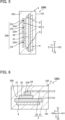
- FIG. 1 is a plan view illustrating an ultrasonic probe 100 according to a first embodiment.
- FIG. 2 is a sectional view of the ultrasonic probe 100 illustrated in FIG. 1 .
- the dimension and the scale of each part of the ultrasonic probe 100 illustrated in FIG. 2 are different from actual ones as appropriate and are schematically illustrated to facilitate understanding. In practice, the thickness of the ultrasonic probe 100 is considerably smaller than that illustrated in FIG. 2.
- FIG. 2 corresponds to a cross-sectional surface taken along line A-A in FIG. 1 .
- an X-axis, a Y-axis, and a Z-axis orthogonal to each other are used as required for the sake of explanations.
- One direction along the X-axis is represented as an X1 direction and the direction opposite to the X1 direction is represented as an X2 direction.
- one direction along the Y-axis is represented as a Y1 direction and the direction opposite to the Y1 direction is represented as a Y2 direction.
- One direction along the Z-axis is represented as a Z1 direction, and the direction opposite to the Z1 direction is represented as a Z2 direction.
- viewing in the Z1 direction or the Z2 direction is referred to as "plan view.” It is envisaged that the Z1 direction represents an upward direction and the Z2 direction represents a downward direction.
- the ultrasonic probe 100 is flexible.
- the flexible ultrasonic probe 100 makes good contact with a curved surface of the neck, the chest, the abdomen, the arms, and the fingers, for example.
- the ultrasonic probe 100 has good contact characteristics not only to a flat surface of a subject, but also with a curved surface.
- the use of the ultrasonic probe 100 can broaden the measurable ranges of a subject.
- the ultrasonic probe 100 includes a piezoelectric element 2, a flexible wiring substrate 3, a backing material 4, and a housing 5. As illustrated in FIG. 2 , the ultrasonic probe 100 has a lower surface 101 and an upper surface 102. The upper surface 102 comes into contact with a subject. The ultrasonic probe 100 transmits and receives ultrasonic waves from the upper surface 102.
- the piezoelectric element 2 illustrated in FIGS. 1 and 2 transmits and receives ultrasonic waves.
- the piezoelectric element 2 mutually converts an electrical signal based on voltage changes to mechanical vibrations of ultrasonic waves, and vice versa.
- the piezoelectric element 2 includes a lower electrode 21, a piezoelectric material 22, and an upper electrode 23.
- the piezoelectric material 22 is between the lower electrode 21 and the upper electrode 23 and is in contact with these electrodes.
- the lower electrode 21 is at a location farther from the subject than the upper electrode 23.
- the lower electrode 21 corresponds to "another electrode” that is in contact with the opposite surface of the piezoelectric material 22 to the upper electrode 23.
- the lower electrode 21 has a lower surface 211 and an upper surface 212.
- the piezoelectric material 22 is in contact with the upper surface 212.
- the thickness of the lower electrode 21 is, for example, preferably not less than 10 ⁇ m and not greater than 200 ⁇ m. The thickness is more preferably not less than 50 ⁇ m and not greater than 100 ⁇ m. A thickness within these ranges maintains flexibility of the ultrasonic probe 100 and practical hardness thereof in contrast to when the thickness is out of these ranges.
- the piezoelectric material 22 has a lower surface 221 and an upper surface 222.
- the lower surface 221 is in contact with the lower electrode 21 and the upper surface 222 is in contact with the upper electrode 23.
- the thickness of the piezoelectric material 22 is preferably not less than 10 ⁇ m and not greater than 200 ⁇ m.
- the thickness is more preferably not less than 50 ⁇ m and not greater than 100 ⁇ m. The thickness within a such range provides easy deformation of the piezoelectric material 22 and easy formation thereof by a sol-gel process, in contrast to when the thickness is out of the range.
- the shape of the upper electrode 23 in plan view is substantially circular.
- the shape may be other than circular, such as polygonal (e.g., rectangular).
- the upper electrode 23 in plan smaller than the lower electrode 21 and the piezoelectric material 22.
- the upper electrode 23 overlaps with the lower electrode 21 and the piezoelectric material 22 in plan view.
- the upper electrode 23 contains a conductive elastomer.
- the conductive elastomer includes a binder and a conductive filler.
- the binder include rubber, such as silicone rubber and urethane rubber, and a thermoplastic elastomer.
- the conductive filler include metallic particles, such as silver powder, conductive carbon, and a plated filler, such as a silver-plated filler.
- the conductive filler may be powder, particles, or fibers.
- the upper electrode 23 with the conductive elastomer enables provision of a thin film and provides high flexibility. This increases the capability of the upper electrode 23 to follow deformation of the piezoelectric material 22.
- the use of the conductive elastomer enables the upper electrode 23 having a sufficient thickness to be formed on the upper surface 222 of the piezoelectric material 22. As a result, a flexible and highly conductive ultrasonic probe 100 is provided.
- the backing material 4 is disposed under the lower electrode 21.
- the backing material 4 is in contact with the lower surface 211 of the lower electrode 21, which is the opposite surface to the piezoelectric material 22.
- the backing material 4 is flexible.
- the backing material 4 attenuates ultrasonic waves emitted downward from the piezoelectric element 2 and suppresses undesired vibrations.
- the provision of the backing material 4 suppresses undesired vibrations and enhances the resolution in contrast when no backing material 4 is provided.
- the provision of the backing material 4 reduces multiple reflections between the lower surface 101 of the ultrasonic probe 100 and the lower surface 211 of the piezoelectric element 2.
- the material of the housing 5 be an elastomer.
- the use of an elastomer as the material for the housing 5 provides a high flexibility, a shock absorbing property, and a water-proof property to protect the piezoelectric element 2.
- an elastomer low in the ultrasonic-wave attenuating property be used as the material of the housing 5, which protects the piezoelectric element 2 and other elements, and acts as an acoustic matching layer.
- Such a housing 5, which contains an elastomer low in the ultrasonic-wave attenuating property protects the piezoelectric element 2 and other elements, and acts as an acoustic matching layer.
- the acoustic matching layer is used to reduce reflection of ultrasonic waves resulting from a difference in acoustic impedance between the piezoelectric element 2 and a subject.
- the acoustic impedance greatly differs between a piezoelectric element 2 and a living body.
- the provision of the housing 5, which acts as the acoustic matching layer reduces reflection of ultrasonic waves resulting from the difference in the acoustic impedance between the piezoelectric element 2 and a living body.
- the housing 5, which acts as the acoustic matching layer improves matching of the acoustic impedance and increases the amount of ultrasonic waves transmitted to the subject.
- the upper electrode 23 is formed, for example, by applying a conductive elastomer onto the piezoelectric material 22 by a screen method and curing the conductive elastomer. Specifically, first, the following are combined to form a conductive elastomer: (i) 100 phr of a binder "KE-106" manufactured by Shin-Etsu Chemical Co., Ltd., (ii) 150 phr of silver filler "FA-2-3" manufactured by DOWA ELECTRONICS MATERIALS CO., Ltd., (iii) 150 phr of silver filler "G-35” manufactured by DOWA ELECTRONICS MATERIALS CO., Ltd., (iv) 10 phr of a curing agent "CAT-RG” manufactured by Shin-Etsu Chemical Co., Ltd., (v) 10 phr of "KF-6015” manufactured by Shin-Etsu Chemical Co., Ltd., and (vi) 10
- the conductive elastomer is applied onto the piezoelectric material 22 with a thickness not less than 50 ⁇ m and not greater than 100 ⁇ m and is cured at 150 °C for 30 minutes. If the conductive elastomer is applied in a substantially circular manner in plan view, the diameter thereof is about not less than 6 mm and not greater than 9 mm.
- the conductive elastomer can be applied onto the piezoelectric material 22 without the material of the upper electrode 23 permeating into the piezoelectric material 22. Furthermore, using the conductive elastomer, the upper electrode 23 with a sufficient thickness can be formed on the piezoelectric material 22, which leads to the ultrasonic probe 100 with a satisfactory conductivity.
- the conductive elastomer contains a binder and a conductive filler.
- the binder is a rubber, such as silicone rubber or urethane rubber or a thermoplastic elastomer. Curing of the binder prevents movement of the conductive filler.
- the use of the conductive elastomer makes it possible to form the upper electrode 23, in which damage (e.g., cracks) is less likely to be produced even when the upper electrode 23 is deformed, and in which decrease in conductivity is suppressed.
- the piezoelectric element 2 is formed by the foregoing processes. As described above, the piezoelectric element 2 includes the piezoelectric material 22 formed by a sol-gel process, and the upper electrode 23 made of the conductive elastomer. As a result, the piezoelectric element 2 is flexible. The flexible piezoelectric element 2 ensures a flexible ultrasonic probe 100. This enables the ultrasonic probe 100 to be applied not only to a flat surface of a subject but also to a curved surface. The applicable range of the ultrasonic probe 100 can be broadened. Furthermore, since the ultrasonic probe 100 is highly flexible, damage, such as cracks, are less likely to occur, and the durability of the ultrasonic probe 100 is improved.
- the wiring 32 of the flexible wiring substrate 3 and the upper electrode 23 are thermocompression-bonded to each other.
- the thermocompression bonding be performed after ultraviolet light is emitted on the surface of the upper electrode 23 to reform the surface. Specifically, vacuum ultraviolet light is applied for 30 seconds using an excimer lamp to reform the surface of the upper electrode 23.
- the wiring 32 and the upper electrode 23 are thermocompression-bonded to each other at 140 °C for 10 seconds using an FPC alignment thermocompression bonding device.
- the wiring 31 of the flexible wiring substrate 3 and the lower electrode 21 are also thermocompression-bonded to each other. Specifically, the wiring 31 and the lower electrode 21 are thermocompression-bonded to each other at 140 °C for 10 seconds using the FPC alignment thermocompression bonding device.
- the housing 5 is formed.
- the housing 5 is formed by sticking a sheet that contains a self-adhesive elastomer with an adhesive to the upper surface 232 of the upper electrode 23 and the lower surface 401 of the backing material 4.
- a self-adhesive silicone rubber sheet is stuck to each of the upper surface 232 and the lower surface 401 with an adhesive.
- the thickness of the sheet that is in contact with the upper surface 232 of the upper electrode 23 is less than that of the thickness of the sheet that is in contact with the lower surface 401 of the backing material 4.
- a self-adhesive silicone rubber sheet with a thickness of 0.4 mm is stuck onto the upper surface 232.
- Another self-adhesive silicone rubber sheet with a thickness of 0.6 mm is stuck onto the lower surface 401.
- the adhesion temperature of the sheet on the upper surface 232 and the sheet of the lower surface 401 is an ordinary temperature, the pressure is 1.2 MPa, and the adhesion time is 30 minutes.
- pressurization may be performed through a foam sheet. For example, after the sheets are stuck to each other, the sheets are left for about 24 hours to obtain a practical strength.
- the ultrasonic probe 100 is manufactured in the forementioned manner. By the foregoing method, a flexible ultrasonic probe 100 with a satisfactory resolution is easily manufactured.
- FIG. 4 is a plan view illustrating an ultrasonic probe 100A according to the second embodiment.
- FIG. 5 is a view of the ultrasonic probe 100A of FIG. 4 as viewed in the X2 direction.
- FIG. 6 is a view of the ultrasonic probe 100A of FIG. 4 as viewed in the Y1 direction.
- the dimensions and the scales of each part of the ultrasonic probe 100A illustrated in FIGS. 4 , 5, and 6 are different from actual ones as appropriate and are schematically illustrated to facilitate understanding.
- FIG. 5 corresponds to a cross-sectional surface taken along line B-B in FIG. 4 .
- FIG. 6 corresponds to a cross-sectional surface taken along line C-C in FIG. 4 .
- the ultrasonic probe 100A of the second embodiment is different from the ultrasonic probe 100 of the first embodiment in having a plurality of piezoelectric elements 2A.
- the ultrasonic probe 100A includes a piezoelectric structure 200, the flexible wiring substrate 3, the backing material 4, and the housing 5.
- the piezoelectric structure 200 includes the piezoelectric elements 2A.
- the ultrasonic probe 100A includes seven piezoelectric elements 2A.
- the number of the piezoelectric elements 2A is not limited thereto. The number may be not less than two and not more than six, or it may be equal to or more than eight.
- the ultrasonic probe 100A may include piezoelectric elements 2A, such as 128 piezoelectric elements 2A.
- the piezoelectric structure 200 includes the lower electrode 21, the piezoelectric material 22, and upper electrodes 23A.
- the lower electrode 21 is provided as one unit in common with the piezoelectric elements 2A.
- the piezoelectric material 22 is provided as one unit in common with the piezoelectric elements 2A.
- the upper electrodes 23A correspond to "electrodes.”
- the upper electrodes 23A are provided one-to-one for the piezoelectric elements 2A.
- the shape of each of the upper electrodes 23A in plan view is rectangular. The shape may be that of a polygon other than a rectangle, or it may be circular.
- the upper electrodes 23A are arranged in a line along the Y-axis spaced apart from each other in plan view.
- the center distance, that is, the pitch of the upper electrodes 23A is, for example, about 0.5 mm although it is not particularly limited thereto.
- the upper electrodes 23A be arranged in a line as illustrated in FIG. 4 .
- the upper electrodes 23A may be arranged in lines or may be arranged in a random manner.
- the wiring 31 is connected to the lower electrode 21 and the wiring 32 is connected to the upper electrodes 23.
- the present embodiment includes piezoelectric elements 2A.
- the upper electrodes 23A are provided one-to-one for the piezoelectric elements 2.
- the piezoelectric material 22 is provided as one unit in common with the piezoelectric elements 2A. As a result, only a portion of the piezoelectric material 22 to which a voltage is applied is vibrated.
- the piezoelectric material 22 is formed by a sol-gel process, and it is porous and thin. Only a portion of the piezoelectric material 22 to which a voltage is applied is adequately vibrated, as long as the upper electrodes 23A are provided for the respective piezoelectric elements 2A without provision of the piezoelectric materials 22 for the respective piezoelectric elements 2A.
- the piezoelectric material 22 is flexible because it is formed by the sol-gel process, and the piezoelectric material 22 is provided as one unit in common with the piezoelectric elements 2A. Therefore, the piezoelectric material 22 has a satisfactory capacity to follow bending of a subject with a curved surface.
- a method for manufacturing the ultrasonic probe 100A includes the processes illustrated in FIG. 3 similarly to the first embodiment.
- the piezoelectric material 22 is formed on the lower electrode 21 by a sol-gel process. Specifically, a sol-gel film with a plan area of 15 mm ⁇ 80 mm and a thickness of about 100 ⁇ m is formed on the lower electrode 21. This sol-gel film is the piezoelectric material 22.
- the upper electrodes 23 are formed, for example, by applying a conductive elastomer onto the piezoelectric material 22 by a screen method and curing the conductive elastomer.
- a conductive elastomer is applied onto the piezoelectric material 22 and is cured at 150 °C for 30 minutes.
- a conductive elastomer is applied in a rectangular pattern having a plan area of 4.5 mm ⁇ 0.25 mm and a thickness of about 50 ⁇ m.
- 128 rectangular patterns are formed. The 128 rectangular patterns are formed with a pitch of 0.5 mm, for example.
- the flexible ultrasonic probe 100A with a satisfactory resolution can be easily manufactured.
- the ultrasonic probe 100 may be an array probe.
Landscapes
- Health & Medical Sciences (AREA)
- Engineering & Computer Science (AREA)
- Life Sciences & Earth Sciences (AREA)
- Physics & Mathematics (AREA)
- Chemical & Material Sciences (AREA)
- General Health & Medical Sciences (AREA)
- Pathology (AREA)
- Manufacturing & Machinery (AREA)
- Mechanical Engineering (AREA)
- General Physics & Mathematics (AREA)
- Biochemistry (AREA)
- Immunology (AREA)
- Analytical Chemistry (AREA)
- Dispersion Chemistry (AREA)
- Heart & Thoracic Surgery (AREA)
- Veterinary Medicine (AREA)
- Molecular Biology (AREA)
- Surgery (AREA)
- Animal Behavior & Ethology (AREA)
- Biomedical Technology (AREA)
- Public Health (AREA)
- Medical Informatics (AREA)
- Acoustics & Sound (AREA)
- Radiology & Medical Imaging (AREA)
- Nuclear Medicine, Radiotherapy & Molecular Imaging (AREA)
- Biophysics (AREA)
- Gynecology & Obstetrics (AREA)
- Ceramic Engineering (AREA)
- Transducers For Ultrasonic Waves (AREA)
Abstract
Description
- The present disclosure relates to ultrasonic probes and to a method for manufacturing ultrasonic probes.
- In medical diagnosis of living bodies and non-destructive testing of structural objects, ultrasonic measurement using an ultrasonic probe is utilized to test an internal structure non-invasively and non-destructively. A general ultrasonic probe has a piezoelectric element that mutually converts an electrical signal based on voltage changes to mechanical vibrations of ultrasonic waves, and vice versa. A general piezoelectric element has a piezoelectric material, an upper electrode disposed on the upper surface of the piezoelectric material, and a lower electrode disposed on the lower surface thereof.
- A flexible ultrasonic probe is desired to enable accurate measurement of a curved part of an object, which means that a flexible piezoelectric element is desired to be included in the ultrasonic probe.
- A piezoelectric material included in a piezoelectric element described in
Patent Document 1 is formed by a sol-gel process to provide flexibility of an ultrasonic probe. An upper electrode included in the piezoelectric element is made of a conductive paste or by a metal deposition method. - Patent Document 1:
WO2013/063676 - A piezoelectric material has large irregularities on its surface because the piezoelectric material formed by the sol-gel process is porous. In forming a metallic film on the piezoelectric material by the deposition method, it is difficult to form a sufficiently thick electrode and the surface of the piezoelectric material cannot be sufficiently covered. As a result, the conductivity of the electrode is deteriorated, resulting in unstable operations of the ultrasonic probe.
- In order to solve the above problems, an ultrasonic probe according to one aspect of the present disclosure includes a piezoelectric element configured to transmit and receive ultrasonic waves. The piezoelectric element includes a piezoelectric material formed by a sol-gel process, and an electrode being in contact with the piezoelectric material and containing a conductive elastomer.
- A method according to another aspect of the present disclosure is a method for manufacturing an ultrasonic probe including a piezoelectric element configured to transmit and receive ultrasonic waves. The method includes manufacturing the piezoelectric element, in which the manufacturing includes forming a piezoelectric material by a sol-gel process, and forming an electrode by applying a conductive elastomer onto the piezoelectric material and curing the conductive elastomer.
- According to the present disclosure, it is possible to provide a flexible ultrasonic probe.
-
-
FIG. 1 is a plan view illustrating an ultrasonic probe according to a first embodiment. -
FIG. 2 is a sectional view of the ultrasonic probe illustrated inFIG. 1 . -
FIG. 3 is a diagram illustrating a flow of a method for manufacturing the ultrasonic probe according to the first embodiment. -
FIG. 4 is a plan view illustrating an ultrasonic probe according to a second embodiment. -
FIG. 5 is a view of the ultrasonic probe ofFIG. 4 as viewed in an X2 direction. -
FIG. 6 is a view of the ultrasonic probe ofFIG. 4 as viewed in a Y1 direction. - Preferred embodiments of the present disclosure are described below with reference to the accompanying drawings. The scope of the present disclosure is not limited to the embodiments unless there are descriptions particularly limiting the present disclosure in the following explanations.
-
FIG. 1 is a plan view illustrating anultrasonic probe 100 according to a first embodiment.FIG. 2 is a sectional view of theultrasonic probe 100 illustrated inFIG. 1 . The dimension and the scale of each part of theultrasonic probe 100 illustrated inFIG. 2 are different from actual ones as appropriate and are schematically illustrated to facilitate understanding. In practice, the thickness of theultrasonic probe 100 is considerably smaller than that illustrated inFIG. 2. FIG. 2 corresponds to a cross-sectional surface taken along line A-A inFIG. 1 . - In the following descriptions, an X-axis, a Y-axis, and a Z-axis orthogonal to each other are used as required for the sake of explanations. One direction along the X-axis is represented as an X1 direction and the direction opposite to the X1 direction is represented as an X2 direction. Similarly, one direction along the Y-axis is represented as a Y1 direction and the direction opposite to the Y1 direction is represented as a Y2 direction. One direction along the Z-axis is represented as a Z1 direction, and the direction opposite to the Z1 direction is represented as a Z2 direction. In the following descriptions, viewing in the Z1 direction or the Z2 direction is referred to as "plan view." It is envisaged that the Z1 direction represents an upward direction and the Z2 direction represents a downward direction.
- The
ultrasonic probe 100 illustrated inFIGS. 1 and 2 are used in ultrasonic measurement, such as medical diagnosis of living bodies and non-destructive testing of structural objects. The ultrasonic measurement is a method for measuring the presence or absence of a subject or the location of the subject by transmitting an ultrasonic signal to the subject from theultrasonic probe 100 and receiving the ultrasonic signal reflected from the subject with theultrasonic probe 100. Ultrasonic waves have a property of reflecting on an interface between different objects. As a difference in acoustic impedance between objects is greater, the reflectance of ultrasonic waves is greater. The presence or absence of a subject or the location of the subject is measured based on the reflectance. With this ultrasonic measurement, an internal structure can be tested non-invasively and non-destructively. - The
ultrasonic probe 100 is flexible. The flexibleultrasonic probe 100 makes good contact with a curved surface of the neck, the chest, the abdomen, the arms, and the fingers, for example. Thus, theultrasonic probe 100 has good contact characteristics not only to a flat surface of a subject, but also with a curved surface. The use of theultrasonic probe 100 can broaden the measurable ranges of a subject. - The
ultrasonic probe 100 includes apiezoelectric element 2, aflexible wiring substrate 3, abacking material 4, and ahousing 5. As illustrated inFIG. 2 , theultrasonic probe 100 has alower surface 101 and anupper surface 102. Theupper surface 102 comes into contact with a subject. Theultrasonic probe 100 transmits and receives ultrasonic waves from theupper surface 102. - The
piezoelectric element 2 illustrated inFIGS. 1 and 2 transmits and receives ultrasonic waves. Thepiezoelectric element 2 mutually converts an electrical signal based on voltage changes to mechanical vibrations of ultrasonic waves, and vice versa. - The
piezoelectric element 2 includes alower electrode 21, apiezoelectric material 22, and anupper electrode 23. Thepiezoelectric material 22 is between thelower electrode 21 and theupper electrode 23 and is in contact with these electrodes. In a state in which theultrasonic probe 100 is in contact with a subject, thelower electrode 21 is at a location farther from the subject than theupper electrode 23. Thelower electrode 21 corresponds to "another electrode" that is in contact with the opposite surface of thepiezoelectric material 22 to theupper electrode 23. - In an example illustrated in
FIG. 1 , the shape of thelower electrode 21 in plan view is rectangular. Thelower electrode 21 is flexible. The material of thelower electrode 21 is, for example, a metal, such as stainless steel. The use of a metallower electrode 21 enables thelower electrode 21 to be a thinner film than an elastomeric one, and to provide hardness of theultrasonic probe 100 to be as low as practical. The material of thelower electrode 21 may be a metal other than stainless steel, or it may be a non-metallic material, such as carbon. - As illustrated in
FIG. 2 , thelower electrode 21 has alower surface 211 and anupper surface 212. Thepiezoelectric material 22 is in contact with theupper surface 212. The thickness of thelower electrode 21 is, for example, preferably not less than 10 µm and not greater than 200 µm. The thickness is more preferably not less than 50 µm and not greater than 100 µm. A thickness within these ranges maintains flexibility of theultrasonic probe 100 and practical hardness thereof in contrast to when the thickness is out of these ranges. - As illustrated in
FIG. 1 , the shape of thepiezoelectric material 22 in plan view is substantially circular. The shape may be other than circular, such as polygonal (e.g., rectangular). In the illustrated example, thepiezoelectric material 22 has its plan area smaller than thelower electrode 21. Thepiezoelectric material 22 overlaps with thelower electrode 21 in plan view. - The
piezoelectric material 22 is a sol-gel film formed by a sol-gel process and is porous. A sol-gel process for forming thepiezoelectric material 22 provides a highly flexiblepiezoelectric material 22. The material of thepiezoelectric material 22 is piezoelectric ceramics, such as lead zirconate titanate (PZT). - As illustrated in
FIG. 2 , thepiezoelectric material 22 has alower surface 221 and anupper surface 222. Thelower surface 221 is in contact with thelower electrode 21 and theupper surface 222 is in contact with theupper electrode 23. The thickness of thepiezoelectric material 22 is preferably not less than 10 µm and not greater than 200 µm. The thickness is more preferably not less than 50 µm and not greater than 100 µm. The thickness within a such range provides easy deformation of thepiezoelectric material 22 and easy formation thereof by a sol-gel process, in contrast to when the thickness is out of the range. - As illustrated in
FIG. 1 , the shape of theupper electrode 23 in plan view is substantially circular. The shape may be other than circular, such as polygonal (e.g., rectangular). In the illustrated example, theupper electrode 23 in plan smaller than thelower electrode 21 and thepiezoelectric material 22. Theupper electrode 23 overlaps with thelower electrode 21 and thepiezoelectric material 22 in plan view. - The
upper electrode 23 contains a conductive elastomer. Preferably, the conductive elastomer includes a binder and a conductive filler. Examples of the binder include rubber, such as silicone rubber and urethane rubber, and a thermoplastic elastomer. Examples of the conductive filler include metallic particles, such as silver powder, conductive carbon, and a plated filler, such as a silver-plated filler. The conductive filler may be powder, particles, or fibers. - The
upper electrode 23 with the conductive elastomer enables provision of a thin film and provides high flexibility. This increases the capability of theupper electrode 23 to follow deformation of thepiezoelectric material 22. The use of the conductive elastomer enables theupper electrode 23 having a sufficient thickness to be formed on theupper surface 222 of thepiezoelectric material 22. As a result, a flexible and highly conductiveultrasonic probe 100 is provided. - Even when the
upper electrode 23 is bent, the flexibleupper electrode 23 suppresses the conductivity thereof from decreasing. If theupper electrode 23 is a metallic film, the flexibility of the material itself is low. When the curvature of theupper electrode 23 is small or when theupper electrode 23 is repeatedly bent, theupper electrode 23 may be damaged. However, the risk of damage (e.g., cracks) to theupper electrode 23 can be reduced even when the curvature of theupper electrode 23 is small or when theupper electrode 23 is repeatedly bent. This is because theupper electrode 23 according to this embodiment is not a metallic film and is highly flexible. As a result, decrease in the conductivity due to minute cracks on theupper electrode 23 is suppressed. Theupper electrode 23 with the conductive elastomer enhances the durability of theultrasonic probe 100. - It is preferable that silicone rubber among the forementioned conductive elastomers be included as the conductive elastomer. Silicone rubber is low in the attenuating property for ultrasonic waves. The use of silicone rubber in the
upper electrode 23 provides a higher-precisionultrasonic probe 100, as compared to use of urethane rubber. - From among the conductive fillers, a silver filler is preferable as the conductive filler. Specifically, a silica core with a silica core material is an example of the silver-plated filler. Silver is highly conductive. A silver filler as the conductive filler provides the highly conductive
upper electrode 23. Furthermore, the conductive filler may include two or more types of fillers differing in average particle diameter. In particular, such anupper electrode 23, which includes two or more types of silver fillers differing in average particle diameter, enhances the performance of theupper electrode 23. - The compound ratio of the conductive filler to 100 phr of the binder is preferably not less than 50 phr and not greater than 600 phr, although it is not particularly limited thereto. The compound ratio is more preferably not less than 100 phr and not greater than 400 phr. The compound ratios within these ranges provide high conductivity and easy formation of the
upper electrode 23 that are less likely to be damaged, in contrast to when the compound ratio is out of these ranges. - For two or more types of conductive fillers differing in the average particle diameter, the average diameter of each of the two types is not particularly limited thereto. The average diameter of one of the two types is preferably not less than 4 µm and not greater than 8 µm. The other average diameter is preferably not less than 5 µm and not greater than 15 µm. With the average diameters equal to or greater than the lower limits, the conductive filler are less likely to aggregate, in contrast to when the average diameters are less than the lower limits. With the average diameters equal to or less than the upper limits, the
upper electrode 23 is less likely to be damaged by bending with a small curvature as compared to a case in which the average diameters are greater than the upper limits. - The conductive elastomer may include a curing agent and a dispersing agent in addition to the binder and the conductive filler described above. Materials other than the forementioned materials may be included without significantly changing the characteristics of the
upper electrode 23. The compound ratio of the curing agent to 100 phr of the binder is, for example, equal to or less than 10 phr. The compound ratio of the dispersing agent to 100 phr of the binder is, for example, equal to or less than 20 phr. Two or more types of each of the curing agent and the dispersing agent may be used. - As illustrated in
FIG. 2 , theupper electrode 23 has alower surface 231 and anupper surface 232. Thelower surface 231 is in contact with thepiezoelectric material 22. Theupper surface 232 is in contact with thehousing 5. The thickness of theupper electrode 23 is preferably not less than 5 µm and not greater than 200 µm. The thickness is more preferably not less than 10 µm and not greater than 100 µm. The thickness within the range allows easier deformation of theupper electrode 23, suppresses attenuation of ultrasonic waves, and makes the thickness of theupper electrode 23 uniform, in contrast to when the thickness is out of the range. - As described above, the
piezoelectric element 2 includes the flexiblelower electrode 21, thepiezoelectric material 22 formed by a sol-gel process, and theupper electrode 23 with the conductive elastomer. As a result, thepiezoelectric element 2 is flexible, which ensures flexibility of theultrasonic probe 100. Theultrasonic probe 100 can be applied not only to a flat surface of a subject but also to a curved surface, which provides wider applicable range of theultrasonic probe 100. Furthermore, the highly flexiblepiezoelectric element 2 enhances the durability of theultrasonic probe 100 because damage (e.g., cracks) is less likely to occur. - The
flexible wiring substrate 3 is connected to thepiezoelectric element 2. Theflexible wiring substrate 3 includes a film insulating substrate, awiring 31 disposed in the insulating substrate, and awiring 32 disposed in the insulating substrate. InFIG. 2 , thewiring 31 and thewiring 32 are schematically illustrated. The insulating substrate is made of a resin such as polyimide. Thewirings wiring 31 is connected to thelower electrode 21. Thewiring 32 is connected to theupper electrode 23. - The
backing material 4 is disposed under thelower electrode 21. Thebacking material 4 is in contact with thelower surface 211 of thelower electrode 21, which is the opposite surface to thepiezoelectric material 22. Thebacking material 4 is flexible. Thebacking material 4 attenuates ultrasonic waves emitted downward from thepiezoelectric element 2 and suppresses undesired vibrations. The provision of thebacking material 4 suppresses undesired vibrations and enhances the resolution in contrast when nobacking material 4 is provided. In addition, the provision of thebacking material 4 reduces multiple reflections between thelower surface 101 of theultrasonic probe 100 and thelower surface 211 of thepiezoelectric element 2. - The shape of the
backing material 4 in plan view is rectangular in the illustrated example. The shape of thebacking material 4 in plan view may be other than rectangular, for example, circular. Thebacking material 4 has its plan area greater than thepiezoelectric material 22 and overlaps with thepiezoelectric material 22 in plan view. Such abacking material 4, which has its plan area greater than thepiezoelectric material 22, more effectively achieves the function to attenuate ultrasonic waves emitted downward from thepiezoelectric material 22, in contrast to abacking material 4 with its small plan area. - It is preferable that the material of the
backing material 4 be an elastomer. The use of an elastomer as the material provides aflexible backing material 4. Specifically, the material of thebacking material 4 is preferably butyl rubber. Butyl rubber has a greater attenuating property for ultrasonic waves than, for example, silicone rubber. The use of butyl rubber as the material of thebacking material 4 attenuates ultrasonic waves sufficiently even when the thickness is small. It is preferable that thebacking material 4 contain no inorganic particles, which increases the flexibility of thebacking material 4 in contrast to use of the inorganic particles. - As illustrated in
FIG. 2 , thebacking material 4 has alower surface 401 and anupper surface 402. Thelower surface 401 is in contact with thehousing 5. Theupper surface 402 is in contact with thepiezoelectric element 2. The thickness of thebacking material 4 is preferably not less than 0.1 mm and not greater than 1.0 mm. The thickness is more preferably not less than 0.2 mm and not greater than 0.8 mm. The thickness within this range provides a highlyflexible backing material 4, and in particular, is more effective in attenuating ultrasonic waves, in contrast to when the thickness is outside of this range. - The
housing 5 illustrated inFIG. 1 covers thepiezoelectric element 2 and thebacking material 4. A part of theflexible wiring substrate 3 is positioned in thehousing 5 and the remaining part is exposed from thehousing 5. Thehousing 5 is flexible. Thehousing 5 protects thepiezoelectric element 2 and other elements. - It is preferable that the material of the
housing 5 be an elastomer. The use of an elastomer as the material for thehousing 5 provides a high flexibility, a shock absorbing property, and a water-proof property to protect thepiezoelectric element 2. It is preferable that an elastomer low in the ultrasonic-wave attenuating property be used as the material of thehousing 5, which protects thepiezoelectric element 2 and other elements, and acts as an acoustic matching layer. Such ahousing 5, which contains an elastomer low in the ultrasonic-wave attenuating property, protects thepiezoelectric element 2 and other elements, and acts as an acoustic matching layer. - The acoustic matching layer is used to reduce reflection of ultrasonic waves resulting from a difference in acoustic impedance between the
piezoelectric element 2 and a subject. For a living body, the acoustic impedance greatly differs between apiezoelectric element 2 and a living body. The provision of thehousing 5, which acts as the acoustic matching layer, reduces reflection of ultrasonic waves resulting from the difference in the acoustic impedance between thepiezoelectric element 2 and a living body. Thehousing 5, which acts as the acoustic matching layer, improves matching of the acoustic impedance and increases the amount of ultrasonic waves transmitted to the subject. - The material of the
housing 5 is preferably silicone rubber. Silicone rubber is lower in ultrasonic-wave attenuating property than urethane rubber and other similar rubbers. Ahousing 5 with silicone rubber is suitably used as the acoustic matching layer and acts as an acoustic lens with an appropriate shape. An acoustic lens is used to focus ultrasonic waves to increase resolution. As a result, the provision of thehousing 5, which acts as an acoustic lens, enhances resolution, in contrast to when ahousing 5 is not provided. Furthermore, silicone rubber is highly biocompatible and is easily use in medical diagnoses of living bodies. Silicone rubber has an acoustic impedance that is similar to that of living bodies. For a living body as the subject, the use of silicone rubber increases the amount of ultrasonic waves transmitted to the subject and enhances resolution. For theupper electrode 23 with silicone rubber, thehousing 5 with silicone rubber also enhances contact therebetween. - It is preferable that inorganic particles not be contained in the
housing 5. If inorganic particles are not used, this increases the flexibility of thehousing 5, in contrast to when inorganic particles are used. The use of elastomers without inorganic particles as materials of thehousing 5 and thebacking material 4 prevents theultrasonic probe 100 from degrading flexibility. As a result, contact with parts of a living body is particularly increased, and a wider range of a living body can be diagnosed. - The shape of the
housing 5 in plan view is rectangular in the illustrated example. The shape of thehousing 5 in plan view may be other than rectangular (e.g., circular). The plan area of thehousing 5, that is, the plan area of theultrasonic probe 100 is not less than 50 mm2 and not greater than 10000 mm2, although this is not particularly limited thereto. - As illustrated in
FIG. 2 , thelower surface 101 of theultrasonic probe 100 corresponds to the lower surface of thehousing 5. Theupper surface 102 corresponds to the upper surface of thehousing 5. The thickness of theultrasonic probe 100 is preferably not less than 0.1 mm and not greater than 10 mm. The thickness is more preferably not less than 0.5 mm and not greater than 2 mm. The thickness within this range provides anultrasonic probe 100 that is highly flexible and is easier to handle, in contrast to when the thickness is outside this range. -
FIG. 3 is a diagram illustrating a flow of a method for manufacturing theultrasonic probe 100 according to the first embodiment. As illustrated inFIG. 3 , the method for manufacturing theultrasonic probe 100 includes a piezoelectric element forming process S10, a wiring forming process S20, a backing material forming process S30, and a housing forming process S40. The piezoelectric element forming process S10 includes a lower electrode preparing process S11, a piezoelectric material forming process S12, and an upper electrode forming process S13. - At the piezoelectric element forming process S10, the
piezoelectric element 2 is formed. Specifically, first, at the lower electrode preparing process S11, thelower electrode 21 is prepared. For example, a stainless steel substrate with a thickness of 50 µm is prepared. - At the piezoelectric material forming process S12, the
piezoelectric material 22 is formed on thelower electrode 21 by a sol-gel process. With the formation of thepiezoelectric material 22 by a sol-gel process, a flexible and thinpiezoelectric material 22 can be easily formed. Specifically, a sol-gel film with a thickness of about 100 µm is formed on thelower electrode 21. - At the upper electrode forming process S13, the
upper electrode 23 is formed, for example, by applying a conductive elastomer onto thepiezoelectric material 22 by a screen method and curing the conductive elastomer. Specifically, first, the following are combined to form a conductive elastomer: (i) 100 phr of a binder "KE-106" manufactured by Shin-Etsu Chemical Co., Ltd., (ii) 150 phr of silver filler "FA-2-3" manufactured by DOWA ELECTRONICS MATERIALS CO., Ltd., (iii) 150 phr of silver filler "G-35" manufactured by DOWA ELECTRONICS MATERIALS CO., Ltd., (iv) 10 phr of a curing agent "CAT-RG" manufactured by Shin-Etsu Chemical Co., Ltd., (v) 10 phr of "KF-6015" manufactured by Shin-Etsu Chemical Co., Ltd., and (vi) 10 phr of "KF-6106" manufactured by Shin-Etsu Chemical Co., Ltd. Next, the conductive elastomer is applied onto thepiezoelectric material 22 with a thickness not less than 50 µm and not greater than 100 µm and is cured at 150 °C for 30 minutes. If the conductive elastomer is applied in a substantially circular manner in plan view, the diameter thereof is about not less than 6 mm and not greater than 9 mm. - Using the conductive elastomer, the conductive elastomer can be applied onto the
piezoelectric material 22 without the material of theupper electrode 23 permeating into thepiezoelectric material 22. Furthermore, using the conductive elastomer, theupper electrode 23 with a sufficient thickness can be formed on thepiezoelectric material 22, which leads to theultrasonic probe 100 with a satisfactory conductivity. - The conductive elastomer contains a binder and a conductive filler. The binder is a rubber, such as silicone rubber or urethane rubber or a thermoplastic elastomer. Curing of the binder prevents movement of the conductive filler. The use of the conductive elastomer makes it possible to form the
upper electrode 23, in which damage (e.g., cracks) is less likely to be produced even when theupper electrode 23 is deformed, and in which decrease in conductivity is suppressed. - The
piezoelectric element 2 is formed by the foregoing processes. As described above, thepiezoelectric element 2 includes thepiezoelectric material 22 formed by a sol-gel process, and theupper electrode 23 made of the conductive elastomer. As a result, thepiezoelectric element 2 is flexible. The flexiblepiezoelectric element 2 ensures a flexibleultrasonic probe 100. This enables theultrasonic probe 100 to be applied not only to a flat surface of a subject but also to a curved surface. The applicable range of theultrasonic probe 100 can be broadened. Furthermore, since theultrasonic probe 100 is highly flexible, damage, such as cracks, are less likely to occur, and the durability of theultrasonic probe 100 is improved. - At the wiring forming process S20, the
flexible wiring substrate 3 connected to thepiezoelectric element 2 is formed. Specifically, theflexible wiring substrate 3 has a part in which a conductive member, such as copper, is exposed. In this case, first, an anisotropic conductive film, which acts as an adhesive member, is temporarily pressure-joined to this part. More specifically, an anisotropic conductive film "MF-331" manufactured by Hitachi Chemical Company, Ltd., is temporarily pressure-joined to a 1.5-millimeter-square exposed part of copper at 80 °C for 3 seconds. - Subsequently, the
wiring 32 of theflexible wiring substrate 3 and theupper electrode 23 are thermocompression-bonded to each other. For theupper electrode 23 made of silicone rubber, it is preferable that the thermocompression bonding be performed after ultraviolet light is emitted on the surface of theupper electrode 23 to reform the surface. Specifically, vacuum ultraviolet light is applied for 30 seconds using an excimer lamp to reform the surface of theupper electrode 23. Subsequently, thewiring 32 and theupper electrode 23 are thermocompression-bonded to each other at 140 °C for 10 seconds using an FPC alignment thermocompression bonding device. Thewiring 31 of theflexible wiring substrate 3 and thelower electrode 21 are also thermocompression-bonded to each other. Specifically, thewiring 31 and thelower electrode 21 are thermocompression-bonded to each other at 140 °C for 10 seconds using the FPC alignment thermocompression bonding device. - In the backing material forming process S30, the
backing material 4 is formed. Specifically, thebacking material 4 is bonded to thelower surface 211 of thelower electrode 21 by applying pressure to form thebacking material 4 on thelower surface 211. If thebacking material 4 contains butyl rubber and thehousing 5 contains silicone rubber, it is preferable that an adhesive butyl rubber tape be used as thebacking material 4. Specifically, a butyl rubber tape "No. 5938" manufactured by Maxell Sliontec Ltd., is bonded as thebacking material 4. - At the housing forming process S40, the
housing 5 is formed. For example, thehousing 5 is formed by sticking a sheet that contains a self-adhesive elastomer with an adhesive to theupper surface 232 of theupper electrode 23 and thelower surface 401 of thebacking material 4. Specifically, a self-adhesive silicone rubber sheet is stuck to each of theupper surface 232 and thelower surface 401 with an adhesive. Given the amount of ultrasonic waves transmitted to a subject, the thickness of the sheet that is in contact with theupper surface 232 of theupper electrode 23 is less than that of the thickness of the sheet that is in contact with thelower surface 401 of thebacking material 4. For example, a self-adhesive silicone rubber sheet with a thickness of 0.4 mm is stuck onto theupper surface 232. Another self-adhesive silicone rubber sheet with a thickness of 0.6 mm is stuck onto thelower surface 401. - For example, if the
housing 5 is made of sheets with silicone rubber, it is preferable that these sheets be stuck to each other after applying ultraviolet light to the surfaces of the sheets to reform the surfaces because silicone rubber is poor in adhesive property. Specifically, the surfaces of the sheets are reformed by applying vacuum ultraviolet light for 30 seconds using an excimer lamp. - The adhesion temperature of the sheet on the
upper surface 232 and the sheet of thelower surface 401 is an ordinary temperature, the pressure is 1.2 MPa, and the adhesion time is 30 minutes. At the time of sticking of the sheets to each other, pressurization may be performed through a foam sheet. For example, after the sheets are stuck to each other, the sheets are left for about 24 hours to obtain a practical strength. - The
ultrasonic probe 100 is manufactured in the forementioned manner. By the foregoing method, a flexibleultrasonic probe 100 with a satisfactory resolution is easily manufactured. - A second embodiment of the present disclosure is explained below. In the embodiment exemplified below, elements having operations and functions identical to those of the first embodiment are denoted by signs used in the explanations of the first embodiment and detailed explanations of such elements are omitted as appropriate.
-
FIG. 4 is a plan view illustrating anultrasonic probe 100A according to the second embodiment.FIG. 5 is a view of theultrasonic probe 100A ofFIG. 4 as viewed in the X2 direction.FIG. 6 is a view of theultrasonic probe 100A ofFIG. 4 as viewed in the Y1 direction. The dimensions and the scales of each part of theultrasonic probe 100A illustrated inFIGS. 4 ,5, and 6 are different from actual ones as appropriate and are schematically illustrated to facilitate understanding.FIG. 5 corresponds to a cross-sectional surface taken along line B-B inFIG. 4 .FIG. 6 corresponds to a cross-sectional surface taken along line C-C inFIG. 4 . - As illustrated in
FIG. 4 ,5, or 6 , theultrasonic probe 100A of the second embodiment is different from theultrasonic probe 100 of the first embodiment in having a plurality ofpiezoelectric elements 2A. - The
ultrasonic probe 100A includes apiezoelectric structure 200, theflexible wiring substrate 3, thebacking material 4, and thehousing 5. Thepiezoelectric structure 200 includes thepiezoelectric elements 2A. In an example illustrated inFIG. 4 , theultrasonic probe 100A includes sevenpiezoelectric elements 2A. However, the number of thepiezoelectric elements 2A is not limited thereto. The number may be not less than two and not more than six, or it may be equal to or more than eight. Specifically, theultrasonic probe 100A may includepiezoelectric elements 2A, such as 128piezoelectric elements 2A. - As illustrated in
FIG. 4 ,5, or 6 , thepiezoelectric structure 200 includes thelower electrode 21, thepiezoelectric material 22, andupper electrodes 23A. Thelower electrode 21 is provided as one unit in common with thepiezoelectric elements 2A. Thepiezoelectric material 22 is provided as one unit in common with thepiezoelectric elements 2A. - The
upper electrodes 23A correspond to "electrodes." Theupper electrodes 23A are provided one-to-one for thepiezoelectric elements 2A. The shape of each of theupper electrodes 23A in plan view is rectangular. The shape may be that of a polygon other than a rectangle, or it may be circular. Theupper electrodes 23A are arranged in a line along the Y-axis spaced apart from each other in plan view. The center distance, that is, the pitch of theupper electrodes 23A is, for example, about 0.5 mm although it is not particularly limited thereto. - It is unnecessary that the
upper electrodes 23A be arranged in a line as illustrated inFIG. 4 . For example, theupper electrodes 23A may be arranged in lines or may be arranged in a random manner. - The
wiring 31 is connected to thelower electrode 21 and thewiring 32 is connected to theupper electrodes 23. - The present embodiment includes
piezoelectric elements 2A. Theupper electrodes 23A are provided one-to-one for thepiezoelectric elements 2. Thepiezoelectric material 22 is provided as one unit in common with thepiezoelectric elements 2A. As a result, only a portion of thepiezoelectric material 22 to which a voltage is applied is vibrated. In particular, thepiezoelectric material 22 is formed by a sol-gel process, and it is porous and thin. Only a portion of thepiezoelectric material 22 to which a voltage is applied is adequately vibrated, as long as theupper electrodes 23A are provided for the respectivepiezoelectric elements 2A without provision of thepiezoelectric materials 22 for the respectivepiezoelectric elements 2A. This results in utilizing thepiezoelectric material 22 for eachupper electrode 23A, even when thepiezoelectric material 22 is not divided. Furthermore, thepiezoelectric material 22 is flexible because it is formed by the sol-gel process, and thepiezoelectric material 22 is provided as one unit in common with thepiezoelectric elements 2A. Therefore, thepiezoelectric material 22 has a satisfactory capacity to follow bending of a subject with a curved surface. - For example, to display images of the
ultrasonic probe 100 for medical use, thepiezoelectric elements 2A are required. By providing thepiezoelectric elements 2A, theultrasonic probe 100 can be used as a phased array probe. - In the present embodiment, a method for manufacturing the
ultrasonic probe 100A includes the processes illustrated inFIG. 3 similarly to the first embodiment. - First, at the lower electrode preparing process S11, the
lower electrode 21 is prepared. Specifically, a stainless steel substrate is prepared with a plan area of 25 mm × 84 mm and a thickness of 50 µm. - At the piezoelectric material forming process S12, the
piezoelectric material 22 is formed on thelower electrode 21 by a sol-gel process. Specifically, a sol-gel film with a plan area of 15 mm × 80 mm and a thickness of about 100 µm is formed on thelower electrode 21. This sol-gel film is thepiezoelectric material 22. - At the upper electrode forming process S13, the
upper electrodes 23 are formed, for example, by applying a conductive elastomer onto thepiezoelectric material 22 by a screen method and curing the conductive elastomer. For example, a conductive elastomer is applied onto thepiezoelectric material 22 and is cured at 150 °C for 30 minutes. Specifically, a conductive elastomer is applied in a rectangular pattern having a plan area of 4.5 mm × 0.25 mm and a thickness of about 50 µm. For example, 128 rectangular patterns are formed. The 128 rectangular patterns are formed with a pitch of 0.5 mm, for example. - In the present embodiment, similarly to the first embodiment, the flexible
ultrasonic probe 100A with a satisfactory resolution can be easily manufactured. - The present disclosure has been described based on the preferred embodiments, but it is not limited to the foregoing embodiments. The configuration of each part in the present disclosure may be replaced with any configuration that provides functions substantially identical to those of the embodiments, or any configuration may be added thereto.
- In the foregoing embodiments, there is one
piezoelectric element 2, but there may be more than onepiezoelectric element 2. That is, theultrasonic probe 100 may be an array probe. - 2... piezoelectric element, 3... flexible wiring substrate, 4... backing material, 5... housing, 21... lower electrode, 22... piezoelectric material, 23... upper electrode, 31... wiring, 32... wiring, 100... ultrasonic probe, 101... lower surface, 102... upper surface, 211... lower surface, 212... upper surface, 221... lower surface, 222... upper surface, 231... lower surface, 232... upper surface, 401... lower surface, 402... upper surface.
Claims (13)
- An ultrasonic probe comprising:at least one piezoelectric element configured to transmit and receive ultrasonic waves,wherein the at least one piezoelectric element comprises:a piezoelectric material formed by a sol-gel process, andat least one electrode being in contact with the piezoelectric material and containing a conductive elastomer.
- The ultrasonic probe according to claim 1, wherein the conductive elastomer contains silicone rubber.
- The ultrasonic probe according to claim 1 or 2, wherein the conductive elastomer contains a conductive filler.
- The ultrasonic probe according to claim 3, wherein the conductive filler is a silver filler.
- The ultrasonic probe according to claim 1, further comprising:another electrode being in contact with a surface of the piezoelectric material opposite to the at least one electrode; anda backing material being in contact with a surface of the another electrode opposite to the piezoelectric material,wherein the backing material contains an elastomer.
- The ultrasonic probe according to claim 5, wherein the backing material contains butyl rubber.
- The ultrasonic probe according to claim 5 or 6, wherein the backing material contains no inorganic particles.
- The ultrasonic probe according to claim 1, further comprising: a housing configured to protect the piezoelectric element,
wherein the housing contains an elastomer. - The ultrasonic probe according to claim 8, wherein the housing contains silicone rubber.
- The ultrasonic probe according to claim 8 or 9, wherein the housing contains no inorganic particles.
- The ultrasonic probe according to claim 1, wherein the piezoelectric material is porous.
- The ultrasonic probe according to claim 1, wherein:the at least one piezoelectric element comprises a plurality of piezoelectric elements,the at least one electrode comprises a plurality of electrodes,the plurality of electrodes are provided corresponding to one-to-one for the plurality of piezoelectric elements, andthe piezoelectric material is provided as one unit for the plurality of piezoelectric elements.
- A method for manufacturing an ultrasonic probe including at least one piezoelectric element configured to transmit and receive ultrasonic waves, the method comprising:manufacturing the at least one piezoelectric element,wherein the manufacturing comprises:forming a piezoelectric material by a sol-gel process; andforming at least one electrode by applying a conductive elastomer onto the piezoelectric material and curing the conductive elastomer.
Applications Claiming Priority (3)
| Application Number | Priority Date | Filing Date | Title |
|---|---|---|---|
| JP2022006067 | 2022-01-19 | ||
| JP2022151759 | 2022-09-22 | ||
| PCT/JP2023/000563 WO2023140166A1 (en) | 2022-01-19 | 2023-01-12 | Ultrasonic probe and ultrasonic probe manufacturing method |
Publications (2)
| Publication Number | Publication Date |
|---|---|
| EP4468743A1 true EP4468743A1 (en) | 2024-11-27 |
| EP4468743A4 EP4468743A4 (en) | 2026-01-07 |
Family
ID=87348787
Family Applications (1)
| Application Number | Title | Priority Date | Filing Date |
|---|---|---|---|
| EP23743161.4A Pending EP4468743A4 (en) | 2022-01-19 | 2023-01-12 | ULTRASOUND PROBE AND METHOD FOR MANUFACTURING AN ULTRASOUND PROBE |
Country Status (4)
| Country | Link |
|---|---|
| US (1) | US20250169367A1 (en) |
| EP (1) | EP4468743A4 (en) |
| JP (1) | JPWO2023140166A1 (en) |
| WO (1) | WO2023140166A1 (en) |
Family Cites Families (20)
| Publication number | Priority date | Publication date | Assignee | Title |
|---|---|---|---|---|
| JPH02196600A (en) * | 1989-01-26 | 1990-08-03 | Ngk Spark Plug Co Ltd | Method of forming split electrode in ultrasonic wave probe |
| JPH067678Y2 (en) * | 1989-02-03 | 1994-02-23 | 日本特殊陶業株式会社 | Piezo rubber ultrasonic probe |
| JP3560998B2 (en) * | 1993-01-27 | 2004-09-02 | 株式会社東芝 | Piezoelectric materials and ultrasonic probes |
| JPH08126090A (en) * | 1994-10-27 | 1996-05-17 | Kanebo Ltd | Forming method for waterproof protective film in manufacture of underwater ultrasonic receiving element |
| JP2009210440A (en) * | 2008-03-04 | 2009-09-17 | Toin Gakuen | Cylindrical cavitation sensor and manufacturing method thereof |
| JP2010136807A (en) * | 2008-12-10 | 2010-06-24 | Konica Minolta Medical & Graphic Inc | Method of manufacturing ultrasonic probe and ultrasonic probe |
| JP2011067485A (en) * | 2009-09-28 | 2011-04-07 | Fujifilm Corp | Ultrasonic transducer and probe |
| EP2540227A1 (en) * | 2010-02-26 | 2013-01-02 | Hitachi Medical Corporation | Ultrasonic probe and ultrasonic image pickup device using same |
| JP5905192B2 (en) * | 2010-07-30 | 2016-04-20 | コニカミノルタ株式会社 | Manufacturing method of ultrasonic probe |
| CA2816935C (en) * | 2010-11-05 | 2020-05-05 | National Research Council Of Canada | Ultrasonic transducer assembly and system for monitoring structural integrity |
| JP5802448B2 (en) * | 2011-06-21 | 2015-10-28 | オリンパス株式会社 | Ultrasonic unit, ultrasonic endoscope, and method of manufacturing ultrasonic unit |
| EP2770510A4 (en) * | 2011-10-17 | 2015-09-16 | Sumitomo Riko Co Ltd | Dielectric film and transducer using same |
| KR101594827B1 (en) * | 2012-04-05 | 2016-02-17 | 엔이씨 도낀 가부시끼가이샤 | Piezoelectric element, piezoelectric vibration module, and manufacturing method of these |
| WO2014119166A1 (en) * | 2013-01-30 | 2014-08-07 | 東海ゴム工業株式会社 | Soft transducer |
| JP6122066B2 (en) * | 2015-06-24 | 2017-04-26 | 国立大学法人 熊本大学 | High frequency ultrasonic piezoelectric element, method for manufacturing the same, and high frequency ultrasonic probe including the same |
| CN107924986B (en) * | 2015-07-16 | 2021-02-23 | 住友理工株式会社 | Piezoelectric sensor |
| JP2018159708A (en) * | 2017-03-23 | 2018-10-11 | 積水化学工業株式会社 | Load detection device |
| WO2018225415A1 (en) * | 2017-06-09 | 2018-12-13 | 国立大学法人熊本大学 | Substrate and method for producing film substrate |
| WO2020075212A1 (en) * | 2018-10-08 | 2020-04-16 | 住友理工株式会社 | Sternal compression training dummy |
| JP7610202B2 (en) * | 2020-11-10 | 2025-01-08 | 天草池田電機株式会社 | Ultrasonic transducer array and manufacturing method thereof |
-
2023
- 2023-01-12 JP JP2023575215A patent/JPWO2023140166A1/ja active Pending
- 2023-01-12 US US18/728,973 patent/US20250169367A1/en active Pending
- 2023-01-12 WO PCT/JP2023/000563 patent/WO2023140166A1/en not_active Ceased
- 2023-01-12 EP EP23743161.4A patent/EP4468743A4/en active Pending
Also Published As
| Publication number | Publication date |
|---|---|
| EP4468743A4 (en) | 2026-01-07 |
| JPWO2023140166A1 (en) | 2023-07-27 |
| WO2023140166A1 (en) | 2023-07-27 |
| US20250169367A1 (en) | 2025-05-22 |
Similar Documents
| Publication | Publication Date | Title |
|---|---|---|
| JP4990272B2 (en) | Ultrasonic probe | |
| US20100198077A1 (en) | Ultrasonic probe | |
| US8758253B2 (en) | Ultrasonic probe and ultrasonic diagnostic apparatus using the same | |
| CN103027711B (en) | Ultrasonic probe and ultrasonovision | |
| EP2227037A1 (en) | Ultrasonic probe, and ultrasonic diagnosis device using the probe | |
| EP2908553A1 (en) | Ultrasonic transducer and method for manufacturing ultrasonic transducer | |
| CN102346022A (en) | Device and system for measuring material thickness | |
| JPWO2004091255A1 (en) | Ultrasonic vibrator and manufacturing method thereof | |
| CN104545994A (en) | Ultrasonic device, ultrasonic probe head, detector, electronic apparatus, and ultrasonic imaging apparatus | |
| JP5406374B2 (en) | Ultrasonic probe and ultrasonic diagnostic apparatus using the same | |
| CN212083324U (en) | A flexible ultrasonic probe and ultrasonic imaging detection system | |
| JP7856323B2 (en) | Ultrasound probe head, ultrasound probe, and ultrasound diagnostic device | |
| CN104545993A (en) | Ultrasonic device, ultrasonic probe, ultrasonic detector and electronic apparatus | |
| CN102105784B (en) | An inspection device | |
| US20250169367A1 (en) | Ultrasonic probe and method for manufacturing ultrasonic probe | |
| CN109387562B (en) | Ultrasonic device | |
| US20250164449A1 (en) | Ultrasonic transducer and method for preparing the same | |
| CN118661431A (en) | Ultrasonic probe and method for manufacturing an ultrasonic probe | |
| US20180161005A1 (en) | Ultrasonic probe | |
| JP3530580B2 (en) | Ultrasonic probe manufacturing method | |
| US11397118B2 (en) | Contact force measuring device and process for measuring a contact force using the contact force measuring device | |
| CN118594896A (en) | Flexible array ultrasonic transducer array with row and column addressing and preparation method thereof | |
| JP6264220B2 (en) | Ultrasonic transducer, ultrasonic probe, and ultrasonic imaging device | |
| JP2012257058A (en) | Ultrasonic vibrator and ultrasonic diagnostic device | |
| JP2012244273A (en) | Ultrasonic probe |
Legal Events
| Date | Code | Title | Description |
|---|---|---|---|
| STAA | Information on the status of an ep patent application or granted ep patent |
Free format text: STATUS: THE INTERNATIONAL PUBLICATION HAS BEEN MADE |
|
| PUAI | Public reference made under article 153(3) epc to a published international application that has entered the european phase |
Free format text: ORIGINAL CODE: 0009012 |
|
| STAA | Information on the status of an ep patent application or granted ep patent |
Free format text: STATUS: REQUEST FOR EXAMINATION WAS MADE |
|
| 17P | Request for examination filed |
Effective date: 20240718 |
|
| AK | Designated contracting states |
Kind code of ref document: A1 Designated state(s): AL AT BE BG CH CY CZ DE DK EE ES FI FR GB GR HR HU IE IS IT LI LT LU LV MC ME MK MT NL NO PL PT RO RS SE SI SK SM TR |
|
| DAV | Request for validation of the european patent (deleted) | ||
| DAX | Request for extension of the european patent (deleted) | ||
| A4 | Supplementary search report drawn up and despatched |
Effective date: 20251208 |
|
| RIC1 | Information provided on ipc code assigned before grant |
Ipc: H04R 17/00 20060101AFI20251202BHEP Ipc: H04R 31/00 20060101ALI20251202BHEP Ipc: A61B 8/00 20060101ALI20251202BHEP Ipc: H10N 30/06 20230101ALI20251202BHEP Ipc: H10N 30/078 20230101ALI20251202BHEP Ipc: H10N 30/30 20230101ALI20251202BHEP Ipc: H10N 30/87 20230101ALI20251202BHEP Ipc: H10N 30/88 20230101ALI20251202BHEP Ipc: B06B 1/06 20060101ALI20251202BHEP |