EP4468723A1 - Imaging device, imaging method, and method for manufacturing imaging device - Google Patents
Imaging device, imaging method, and method for manufacturing imaging device Download PDFInfo
- Publication number
- EP4468723A1 EP4468723A1 EP22847394.8A EP22847394A EP4468723A1 EP 4468723 A1 EP4468723 A1 EP 4468723A1 EP 22847394 A EP22847394 A EP 22847394A EP 4468723 A1 EP4468723 A1 EP 4468723A1
- Authority
- EP
- European Patent Office
- Prior art keywords
- optical
- electric
- electric signal
- computing
- signal
- Prior art date
- Legal status (The legal status is an assumption and is not a legal conclusion. Google has not performed a legal analysis and makes no representation as to the accuracy of the status listed.)
- Pending
Links
- 238000003384 imaging method Methods 0.000 title claims abstract description 98
- 238000004519 manufacturing process Methods 0.000 title claims description 12
- 238000000034 method Methods 0.000 title claims description 9
- 230000003287 optical effect Effects 0.000 claims abstract description 241
- 238000010801 machine learning Methods 0.000 claims description 11
- 230000005415 magnetization Effects 0.000 description 32
- 238000009826 distribution Methods 0.000 description 14
- 238000006243 chemical reaction Methods 0.000 description 5
- 239000011159 matrix material Substances 0.000 description 5
- 230000000694 effects Effects 0.000 description 3
- CIWBSHSKHKDKBQ-JLAZNSOCSA-N Ascorbic acid Chemical compound OC[C@H](O)[C@H]1OC(=O)C(O)=C1O CIWBSHSKHKDKBQ-JLAZNSOCSA-N 0.000 description 2
- 230000000295 complement effect Effects 0.000 description 2
- 230000007423 decrease Effects 0.000 description 2
- 230000006870 function Effects 0.000 description 2
- 239000000696 magnetic material Substances 0.000 description 2
- 229910044991 metal oxide Inorganic materials 0.000 description 2
- 150000004706 metal oxides Chemical class 0.000 description 2
- 230000010287 polarization Effects 0.000 description 2
- 239000004065 semiconductor Substances 0.000 description 2
- 238000003860 storage Methods 0.000 description 2
- 229910019236 CoFeB Inorganic materials 0.000 description 1
- 230000005374 Kerr effect Effects 0.000 description 1
- 230000005540 biological transmission Effects 0.000 description 1
- 230000003111 delayed effect Effects 0.000 description 1
- 239000004973 liquid crystal related substance Substances 0.000 description 1
- 229910000889 permalloy Inorganic materials 0.000 description 1
- 230000001105 regulatory effect Effects 0.000 description 1
- 230000004044 response Effects 0.000 description 1
Images



Classifications
-
- H—ELECTRICITY
- H04—ELECTRIC COMMUNICATION TECHNIQUE
- H04N—PICTORIAL COMMUNICATION, e.g. TELEVISION
- H04N23/00—Cameras or camera modules comprising electronic image sensors; Control thereof
- H04N23/95—Computational photography systems, e.g. light-field imaging systems
-
- H—ELECTRICITY
- H04—ELECTRIC COMMUNICATION TECHNIQUE
- H04N—PICTORIAL COMMUNICATION, e.g. TELEVISION
- H04N23/00—Cameras or camera modules comprising electronic image sensors; Control thereof
- H04N23/50—Constructional details
- H04N23/55—Optical parts specially adapted for electronic image sensors; Mounting thereof
-
- H—ELECTRICITY
- H04—ELECTRIC COMMUNICATION TECHNIQUE
- H04N—PICTORIAL COMMUNICATION, e.g. TELEVISION
- H04N23/00—Cameras or camera modules comprising electronic image sensors; Control thereof
- H04N23/80—Camera processing pipelines; Components thereof
-
- H—ELECTRICITY
- H04—ELECTRIC COMMUNICATION TECHNIQUE
- H04N—PICTORIAL COMMUNICATION, e.g. TELEVISION
- H04N23/00—Cameras or camera modules comprising electronic image sensors; Control thereof
- H04N23/80—Camera processing pipelines; Components thereof
- H04N23/815—Camera processing pipelines; Components thereof for controlling the resolution by using a single image
-
- H—ELECTRICITY
- H04—ELECTRIC COMMUNICATION TECHNIQUE
- H04N—PICTORIAL COMMUNICATION, e.g. TELEVISION
- H04N25/00—Circuitry of solid-state image sensors [SSIS]; Control thereof
- H04N25/40—Extracting pixel data from image sensors by controlling scanning circuits, e.g. by modifying the number of pixels sampled or to be sampled
- H04N25/41—Extracting pixel data from a plurality of image sensors simultaneously picking up an image, e.g. for increasing the field of view by combining the outputs of a plurality of sensors
Definitions
- the present invention relates to an imaging device and an imaging method for generating an electric signal indicative of an image with use of optical computing, and a method for producing the imaging device.
- An imaging device including an optical system constituted by a plurality of lenses (see, for example, Patent Literature 1) and an image sensor typified by, for example, a charge coupled device (CCD) and a complementary metal oxide semiconductor (CMOS) is widely used.
- Examples of such an imaging device include a digital still camera and a digital video camera.
- imaging devices Most of these imaging devices that are commercially available are of the type called camcorders in which an image sensor and a storage section are integrated with each other. However, some of the imaging devices are of the type, such as endoscopes used in medical practice, in which the image sensor and the storage section are separated from each other.
- the optical system of such an imaging device is configured to form an image of a subject on a light receiving surface of an image sensor.
- Such a configuration of the optical system allows the image sensor to generate an electric signal indicative of an image that focuses on the subject.
- Patent Literature 1 Japanese Patent Application Publication Tokukai No. 2020-086357
- an imaging device that forms an image of a subject on a light receiving surface with use of an optical system captures a new image of the subject every time the imaging device generates an electric signal indicative of a different image.
- the imaging device it is difficult for the imaging device to generate electric signals indicative of different images fast or frequently.
- the different images include images captured at different angles of view, images having different resolutions, and images having different focal depths (images differing in point of focus).
- An aspect of the present invention has been accomplished in view of the foregoing problem. It is an object of the present invention to achieve an imaging device and an imaging method that are able to generate, from an electric signal including one and the same piece of image information, an electric signal including different image information, and a method for producing the imaging device.
- an imaging device in accordance with an aspect of the present invention includes: an optical computing section configured to perform optical computing with respect to a first optical signal to generate a second optical signal including a feature amount extracted from the first optical signal; an image sensor configured to convert the second optical signal into a first electric signal; and an electric computing section configured to perform electric computing with respect to the first electric signal to generate a second electric signal.
- the present imaging device employs a configuration such that the electric computing section has a plurality of models for each generating the second electric signal from the first electric signal, and the second electric signal generated through the electric computing performed with respect to the first electric signal including one and the same piece of image information with use of each of the models includes different image information.
- an imaging method in accordance with an aspect of the present invention includes: an optical computing step of performing optical computing with respect to a first optical signal to generate a second optical signal including a feature amount extracted from the first optical signal; a converting step of converting the second optical signal into a first electric signal; and an electric computing step of performing electric computing with respect to the first electric signal to generate a second electric signal.
- the present imaging method employs a configuration such that the electric computing step is achieved with use of a plurality of models for each generating the second electric signal from the first electric signal, and the second electric signal generated through the electric computing performed with respect to the first electric signal with use of each of the models includes different image information.
- a method for producing an imaging device in accordance with an aspect of the present invention is a method for producing an imaging device in accordance with the above-described aspect of the present invention, the method including a step of designing the optical computing section and the plurality of models by machine learning so that, in a case where electric computing has been performed with respect to the first electric signal with use of each of the models, the second electric signal including different image information is generated.
- an imaging device and an imaging method that are able to generate, from an electric signal including one and the same piece of image information, an electric signal including different image information, and a method for producing the imaging device.
- FIG. 1 is a schematic view illustrating a configuration of an imaging device 1.
- (a) of Fig. 2 is an elevation view illustrating a tree that is an example of a subject.
- (b) is a view illustrating an example of an optical signal L2 that an optical computing section 11 of the imaging device 1 generates.
- Each of (a) to (c) of Fig. 3 is a view illustrating an example of an image indicated by each of electric signals E2 that an electric computing section 13 of the imaging device 1 generates.
- the imaging device 1 includes the optical computing section 11, an image sensor 12, the electric computing section 13, and a display 14.
- the imaging device 1 may further include an optical system that is provided so as to be followed by the optical computing section 11.
- the optical system includes a plurality of lenses.
- the optical system causes light transmitted toward the optical computing section 11 to enter, as an optical signal L1, the optical computing section 11.
- Examples of light transmitted toward the optical computing section 11 include an image of a subject and an image displayed by a display device which is called a display or a monitor.
- the image of the subject is constituted by object light, which is light reflected and/or scattered by the subject.
- this optical system is preferably configured such that the image of the subject is not formed on a light receiving surface of an image sensor 12 that will be described later.
- the image sensor 12 is preferably disposed such that the image of the subject is not formed on the light receiving surface of the image sensor 12.
- the optical computing section 11 includes a plurality of optical modulation elements stacked in order on top of each other.
- optical modulation elements 111 to 114 are used as the plurality of optical modulation elements.
- Each optical modulation element 11i is an example of a transmissive optical modulation element.
- i is any natural number of not less than 1 and not more than n.
- i 4.
- a specific example of each optical modulation element 11i will be described later with reference to Figs. 4 and 5 .
- a specific optical path on which the optical signal L1 travels is a linear optical path through each optical modulation element 11i.
- the optical system may or may not be provided so as to be followed by the optical computing section 11, but in either case, the optical signal L1 (see (a) of Fig. 2 ) indicative of the image of the subject enters the light receiving surface of the optical computing section 11.
- the optical signal L1 is an example of a first optical signal.
- the optical computing section 11 performs optical computing with respect to the optical signal L1 to generate the optical signal L2 including a feature amount extracted from the optical signal L1.
- an image indicated by the optical signal L2 has a two-dimensional intensity distribution (that is, a two-dimensional optical pattern).
- An image illustrated in (b) of Fig. 2 is an example of the optical signal L2.
- the image sensor 12 converts the optical signal L2 entering a light receiving surface of the image sensor 12 into the electric signal E1.
- the electric signal E1 is an example of a first electric signal.
- the image sensor 12 includes a plurality of pixels arranged in a matrix manner. The image sensor 12 detects the intensity of light entering each pixel and generates an electric signal corresponding to the intensity of the light.
- the image sensor 12 may be a charge coupled device (CCD) or may be a complementary metal oxide semiconductor (CMOS).
- CMOS complementary metal oxide semiconductor
- a form of the image sensor 12 is not particularly limited, but can be selected as appropriate.
- a monochrome image sensor is employed as the image sensor 12.
- a color image sensor may be employed as the image sensor 12.
- the electric computing section 13 performs electric computing with respect to the electric signal E1 to generate the electric signal E2.
- the electric computing section 13 has a plurality of models for each generating, from the electric signal E1, the electric signal E2.
- the description of the present embodiment assumes that the electric computing section 13 has first to third models as the plurality of models.
- the number of the models included in the electric computing section 13 is not limited to three, but can be determined as appropriate.
- the electric computing section 13 may have 10 models or may have 100 models.
- the electric computing section 13 performs, with use of the first to third models, electric computing with respect to the electric signal E1 having one and the same piece of image information to generate the electric signals E2 having respectively different pieces of image information, the electric signals E2 being different from each other as illustrated in (a) to (c) of Fig. 3 .
- the electric signal E1 may include one and the same piece of image information
- the electric signals E2 may include respectively different pieces of image information. That is, the expression "the electric signal having image information” may be construed as indicating "the electric signal including image information" or "the electric signal indicative of an image".
- the invention of the present application also encompasses an imaging method performed in the imaging device 1, the method including: an optical computing step of performing optical computing with respect to the optical signal L1 to generate the optical signal L2; a converting step of converting the optical signal L2 into the electric signal E1; and an electric computing step of performing electric computing with respect to the electric signal E1 to generate the electric signal E2.
- the electric computing step can be performed with use of a plurality of models (in the present embodiment, first to third models) for generating, from the electric signal E1, the electric signals E2, and the electric signal E2 generated through the electric computing performed with respect to the electric signal E1 with use of each of the models has different image information.
- An image illustrated in (a) of Fig. 3 is an example of an image corresponding to a case where an angle of view of a zoom lens is narrow.
- An image illustrated in (c) of Fig. 3 is an example of an image corresponding to a case where the angle of view of the zoom lens is wide.
- An image illustrated in (b) of Fig. 3 is an example of an image corresponding to a case where the angle of view of the zoom lens is intermediate between the angle of view corresponding to the image illustrated in (a) of Fig. 3 and the angle of view corresponding to the image illustrated in (c) of Fig. 3 .
- the electric computing section 13 changes, in this way, a parameter corresponding to the angle of view of the zoom lens to generate, from the electric signal E1 indicative of one and the same image, the electric signals E2 indicative of a plurality of images having different angles of view.
- the plurality of images indicated by the electric signals E2 may have respectively different angles of view as illustrated in (a) to (c) of Fig. 3 , may have respectively different resolutions, or may have respectively different focal depths. Furthermore, the plurality of images indicated by the electric signals E2 may have respectively different combinations of an angle of view, a resolution, and a focal depth.
- the optical computing section 11 and the first to third models are designed by machine learning so that the electric signals E2 indicative of different images are generated in a case where the electric computing has been performed with respect to the electric signal E1 with use of the first to third models.
- the present invention encompasses a method for producing the imaging device 1, the method including the step of designing the optical computing section 11 and the first to third models by machine learning so that the electric signals E2 having different pieces of image information are generated in a case where the electric computing has been performed on the electric signal E1 with use of the first to third models.
- the imaging device 1 is configured to be capable of receiving input from a user with use of a user interface that is not illustrated in Fig. 1 .
- This user interface may be a keyboard, may be a mouse, or may be a touch panel which is provided on a display panel of a display 14 (described later).
- a user can use the user interface to input, to the imaging device 1, user selection information indicating which of the first to third models is to be selected.
- the electric computing section 13 also can generate the electric signal E2 from the electric signal E1 with use of a model which has been selected by the user from among the first to third models according to the content of the user selection information.
- Fig. 1 schematically illustrates a case where the user selects the first model from among the first to third models, the electric computing section 13, in response to the user selection information, generates the electric signal E2 from the electric signal E1 with use of the first model, and the image illustrated in (a) of Fig. 3 (image indicated by the electric signal E2) is displayed on the display 14.
- the imaging device 1 performs electric computing with respect to the electric signal E1 indicative of one and the same image to generate, without performing a new image capture, the electric signals E2 indicative of images which differ in at least one of the angle of view, resolution, and focal depth.
- the imaging device 1 is suitably used in a case where an image of a certain subject is captured from a predetermined angle, and zoomed-in images of a plurality of predetermined areas in the subject are checked. Examples of the imaging device used in such a way include an endoscope used in medical practice.
- the display 14 acquires the electric signal E2 generated by the electric computing section 13 and then displays the image indicated by the electric signal E2.
- the display 14 may be a liquid crystal display, may be an organic LED display, or may be a plasma display.
- the touch panel which is an example of the above-described user interface, may be provided on the display panel of the display 14.
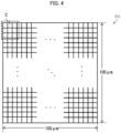
- Fig. 4 is a plan view of the optical modulation element 11i in accordance with the present specific example.
- Fig. 5 is a partial enlarged perspective view illustrating the optical modulation element 11i in accordance with the present specific example (illustrating a portion enclosed by a dotted line in Fig. 4 ) in an enlarged manner.
- the optical modulation element 11i is an example of a transmissive optical modulation element.
- the optical modulation element 11i is constituted by a plurality of microcells C having phase modulation amounts set independently of each other.
- the optical signal L1 enters the optical modulation element 11i, resulting optical signals L1 phase-modulated by the microcells C interfere with each other.
- This achieves a predetermined optical computing (conversion of a two-dimensional intensity distribution in accordance with a predetermined conversion rule).
- the phase modulation amounts of the microcells C may be variable or may be fixed. In the present specific example, the phase modulation amounts are fixed.
- the "microcell” refers to, for example, a cell having a cell size of less than 10 ⁇ m
- the "cell size” refers to a square root of an area of a cell.
- the cell size of the microcell C is a length of a side of the microcell C.
- the lower limit of the cell size of the microcell C is, for example, 1 nm.
- the optical modulation element 11i exemplified in Fig. 4 is constituted by 200 ⁇ 200 microcells C arranged in a matrix manner.
- Each microcell C has a square shape with a size of 500 nm ⁇ 500 nm in a plan view
- the optical modulation element 11i has a square shape with a size of 100 ⁇ m ⁇ 100 ⁇ m in a plan view.
- the phase modulation amount of signal light transmitted through each microcell C can be set for each cell independently by (1) a method in which a thickness of the microcell C is set for each cell independently or (2) a method in which a refractive index of the microcell C is selected for each cell independently.
- the method (1) which can be achieved by nanoimprinting, is employed.
- each microcell C is constituted by a quadratic prism-shaped pillar having a square bottom surface with four sides that are all equal to the cell size.
- the phase modulation amount of the signal light transmitted through each microcell C is determined depending on a height of the pillar constituting the corresponding microcell C.
- the phase modulation amount of the signal light transmitted through the microcell C increases, and as the height of the pillar constituting the microcell C decreases, the phase modulation amount of the signal light transmitted through the microcell C decreases.
- the setting of the phase modulation amount of each microcell C can be achieved by machine learning.
- a model used in the machine learning is, for example, a model to which a two-dimensional intensity distribution of the optical signal L1 input to the optical modulation element 11i is input, and from which the two-dimensional intensity distribution of the optical signal L2 output from the optical modulation element 11i is output, the model including the phase modulation amount of each microcell C as a parameter.
- the two-dimensional intensity distribution of the optical signal L1 input to the optical modulation element 11i refers to a set of intensities of signal light beams input to microcells C that constitute the optical modulation element 11i.
- the two-dimensional intensity distribution of the optical signal L2 output from the optical modulation element 11i refers to a set of intensities of signal light beams input to microcells C that constitute an optical modulation element 11i+1 which is disposed so as to follow the optical modulation element 11i or a set of intensities of signal light beams input to pixels that constitute the image sensor 12 which is disposed so as to follow the optical modulation element 11i.
- FIG. 6 is a schematic view illustrating a configuration of an optical computing section 11A included in the imaging device according to the present variation.
- the imaging device according to the present variation can be obtained by replacing the optical computing section 11 included in the imaging device 1 illustrated in Fig. 1 with an optical computing section 11A.
- the optical computing section 11A will be described, but the image sensor 12, the electric computing section 13, and the display 14 will not be described.
- each optical modulation element included in the optical computing section 11 may be a reflective optical modulation element.
- the optical computing section 11A includes a plurality of optical modulation element 11Ai (in the present specific example, optical modulation elements 11A1 to 11A4).
- the optical modulation element 11Ai like the optical modulation element 11i, has an optical computing function, that is, a function of converting the two-dimensional intensity distribution of the optical signal L1 in accordance with a predetermined conversion rule. This allows the two-dimensional intensity distribution of the optical signal L1 reflected by the optical modulation element 11Ai to be converted into the two-dimensional intensity distribution of the optical signal L2.
- an optical computing function that is, a function of converting the two-dimensional intensity distribution of the optical signal L1 in accordance with a predetermined conversion rule.
- an optical modulation element 11A1 at a first stage is disposed such that the optical signal L1 enters a reflective surface of the optical modulation element 11A1 at an incident angle of 45 degrees.
- An optical modulation element 11A2 at a second stage is disposed such that a portion of a reflective surface of the optical modulation element 11A2 faces a portion of the reflective surface of the optical modulation element 11A1, and such that the respective reflective surfaces of the optical modulation elements 11A1 and 11A2 are parallel to each other.
- An optical signal on which the optical modulation element 11A1 has performed optical computing is emitted from the reflective surface of the optical modulation element 11A1 at an emission angle of 45 degrees.
- an optical modulation element 11A3 at a third stage is disposed such that a portion of a reflective surface of the optical modulation element 11A3 faces another portion of the reflective surface of the optical modulation element 11A2, and the respective reflective surfaces of the optical modulation elements 11A2 and 11A3 are parallel to each other.
- An optical modulation element 11A4 at a fourth stage is disposed such that a portion of a reflective surface of the optical modulation element 11A4 faces another portion of the reflective surface of the optical modulation element 11A3, and the respective reflective surfaces of the optical modulation elements 11A3 and 11A4 are parallel to each other.
- a specific optical path on which the optical signal L1 travels is a zigzag optical path passing each optical modulation element 11Ai.
- FIG. 7 is a cross-sectional view of a microcell C constituting the optical modulation element 11Ai in accordance with the present specific example.
- the optical modulation element 11Ai is an example of a reflective optical modulation element.
- the optical modulation element 11Ai like the optical modulation element 11i illustrated in Fig. 4 , includes a plurality of microcells C.
- the phase modulation amounts are set for the microcells C independently of each other.
- the phase modulation amounts of the microcells C may be variable or may be fixed. In the present specific example, the phase modulation amounts are variable.
- the optical modulation element 11Ai is, as with the optical modulation element 11i illustrated in Fig. 4 , constituted by 200 ⁇ 200 microcells arranged in a matrix manner. Each microcell has a square shape with a size of 500 nm ⁇ 500 nm in a plan view.
- the optical modulation element 11Ai has a square shape with a size of 100 ⁇ m ⁇ 100 ⁇ m in a plan view.
- each microcell C constituting the optical modulation element 11Ai may include a polarizing plate C11, a reflecting plate C12, a first electrode C13, a magnetization free layer C14, an insulating layer C15, a magnetization fixed layer C16, and a second electrode C17.
- the polarizing plate C11 and the reflecting plate C12 are disposed opposite to each other.
- the first electrode C13, the magnetization free layer C14, the insulating layer C15, the magnetization fixed layer C16, and the second electrode C17 are stacked in this order, and are sandwiched between the polarizing plate 11 and the reflecting plate 12.
- a direction in which the first electrode C13, the magnetization free layer C14, the insulating layer C15, the magnetization fixed layer C16, and the second electrode C17 are stacked is orthogonal to a direction in which the polarizing plate C11 and the reflecting plate C12 are stacked.
- a first side surface of the magnetization free layer C14 is in surface contact with one main surface of the polarizing plate C11, and a second side surface of the magnetization free layer C14 which is located opposite the first side surface of the magnetization free layer C14 is in surface contact with one main surface of the reflecting plate C12.
- Signal light L (1) enters an inside of the magnetization free layer C14 through the polarizing plate C11, (2) is reflected by the reflecting plate C12 and (3) is emitted through the polarizing plate C11 to an outside of the magnetization free layer C14.
- the magnetization free layer C14 is made of, for example, an electrically conductive, light-transmissive, soft magnetic material (for example, CoFeB).
- the magnetization fixed layer C16 is made of, for example, an electrically conductive hard magnetic material (for example, permalloy).
- Selected as the polarizing plate C11 is a polarizing plate that selectively transmits a polarized light component having a polarization direction P parallel to a magnetization direction M of the magnetization fixed layer C16.
- Fig. 6 exemplifies a case that the magnetization direction M and the polarization direction P are parallel to both a main surface of the polarizing plate C11 and a main surface of the magnetization fixed layer C16.
- a tunnel effect occurs and injects a spin flow (a flow of spin-polarized electrons) from the magnetization fixed layer C16 through the insulating layer C15 into the magnetization free layer C14 to magnetize the magnetization free layer C14.
- the magnetization occurring in the magnetization free layer C14 is parallel to the magnetized direction M of the magnetization fixed layer C16, that is, a magnetization parallel to the polarized direction P of the signal light entering the magnetization free layer C14 through the polarizing plate 11. This causes a phase of the signal light to be delayed by a transverse Kerr effect during a process of transmission in the magnetization free layer C14.
- a phase modulation amount of the cell C is determined depending on a magnitude of the magnetization in the magnetization free layer C14.
- the magnitude of the magnetization in the magnetization free layer C14 is determined depending on a magnitude of the spin flow injected into the magnetization free layer C14.
- the magnitude of the spin flow injected into the magnetization free layer C14 is determined depending on the potential difference provided between the first electrode C13 and the second electrode C17.
- the setting of the phase modulation amount of each microcell C can be achieved by, for example, machine learning.
- a model used in the machine learning is, for example, a model to which a two-dimensional intensity distribution of the signal light input to the optical modulation element 11Ai is input, and from which the two-dimensional intensity distribution of the signal light output from the optical modulation element 11Ai is output, the model including the phase modulation amount of each microcell C as a parameter.
- the two-dimensional intensity distribution of the signal light input to the optical modulation element 11Ai refers to a set of intensities of signal light beams input to microcells C that constitute the optical modulation element 11Ai.
- the two-dimensional intensity distribution of the signal light output from the optical modulation element 11Ai refers to a set of intensities of signal light beams input to microcells C that constitute an optical modulation element 11Ai+1 which is disposed so as to follow the optical modulation element 11Ai or a set of intensities of signal light beams input to cells that constitute the two-dimensional image sensor which is disposed so as to follow the optical modulation element 11Ai.
- An imaging device in accordance with Aspect 1 of the present invention includes: an optical computing section configured to perform optical computing with respect to a first optical signal to generate a second optical signal including a feature amount extracted from the first optical signal; an image sensor configured to convert the second optical signal into a first electric signal; and an electric computing section configured to perform electric computing with respect to the first electric signal to generate a second electric signal.
- the present imaging device employs a configuration such that the electric computing section has a plurality of models for each generating the second electric signal from the first electric signal, and the second electric signal generated through the electric computing performed with respect to the first electric signal including one and the same piece of image information with use of each of the models includes different image information.
- the present imaging device enables, through electric computing performed with respect to the first electric signal having one and the same piece of image information, the generation of second electric signals including respectively different pieces of image information.
- An imaging device in accordance with Aspect 2 of the present invention employs, in addition to the configuration of the imaging device in accordance with Aspect 1 described above, a configuration such that the optical computing section and the plurality of models are designed by machine leaning so that, in a case where electric computing has been performed with respect to the first electric signal with use of each of the models, the second electric signal indicative of a different image is generated.
- An imaging device in accordance with an aspect of the present invention employs, in addition to the configuration of the imaging device in accordance with Aspect 1 or 2 described above, a configuration such that the electric computing section generates, from the first electric signal, the second electric signal with use of a model selected by a user from among the plurality of models.
- An imaging device in accordance with Aspect 3 of the present invention employs, in addition to the configuration of the imaging device in accordance with Aspect 1 described above, a configuration such that the second electric signal generated through the electric computing performed with respect to the first electric signal with use of each of the models indicates an image differing in angle of view.
- the conventional imaging device In order to generate an electric signal including image information differing in angle of view, the conventional imaging device would need to, for the change of the angle of view, mechanically change a position of the lens included in the optical system, and capture an image of a subject again. According to the above configuration, it is possible to generate the second electric signal including image information differing in angle of view, without mechanically changing the position of the lens or capturing the image of the subject again. This makes it possible to accelerate the generation of the second electric signal.
- An imaging device in accordance with Aspect 4 of the present invention employs, in addition to the configuration of the imaging device in accordance with Aspect 1 or 2 described above, a configuration such that the second electric signal generated through the electric computing performed with respect to the first electric signal with use of each of the models includes image information differing in resolution.
- the conventional imaging device would change a resolution, which is one of image capture conditions set in advance before an image capture, and then capture an image of a subject again.
- a resolution which is one of image capture conditions set in advance before an image capture
- the second electric signal including image information differing in resolution. This makes it possible to accelerate the generation of the second electric signal.
- An imaging device in accordance with Aspect 5 of the present invention employs, in addition to the configuration of the imaging device in accordance with Aspect 1 or 2 described above, a configuration such that the second electric signal generated through the electric computing performed with respect to the first electric signal with use of each of the models includes image information differing in focal depth.
- the conventional imaging device In order to generate an electric signal including image information differing in focal depth, the conventional imaging device would need to, for the change of the focal depth, mechanically change a position of the lens included in the optical system and capture an image of a subject again. According to the above configuration, it is possible to generate, without mechanically changing the position of the lens or capturing the image of the object again, the second electric signal including image information differing in focal depth. This makes it possible to accelerate the generation of the second electric signal.
- An imaging device in accordance with Aspect 6 of the present invention employs, in addition to the configuration of the imaging device in accordance with any one of Aspects 1 to 5 described above, a configuration such that the image sensor is disposed such that an image of a subject is not formed on a light receiving surface of the image sensor.
- one of directions included in an angle of view of the image sensor corresponds, on a one-to-one basis, to one of a plurality of pixels included in the image sensor and arranged in a matrix manner.
- the image of the subject is not formed on the light receiving surface of the image sensor. Therefore, one of the directions included in the angle of view of the image sensor corresponds, on a one-to-multiple basis to the plurality of pixels included in the image sensor and arranged in a matrix manner.
- the first electric signal generated in the condition where the one of the directions corresponds to the plurality of pixels on the one-to-multiple basis is preferable to use. This is because the first electric signal generated in such a condition includes various types of information.
- An imaging device in accordance with Aspect 7 of the present invention employs, in addition to the configuration of the imaging device in accordance with any one of Aspects 1 to 7 described above, a configuration such that the optical computing section includes at least one transmissive optical modulation element that is constituted by a plurality of microcells having respective thicknesses or respective refractive indexes which are set independently of each other, and a specific optical path on which the first optical signal travels passes the at least one transmissive optical modulation element included in the optical computing section.
- a plurality of microcells having respective thicknesses or respective refractive indexes which are set independently of each other are suitably used as the transmissive optical modulation element.
- An imaging device in accordance with Aspect 8 of the present invention employs, in addition to the configuration of the imaging device in accordance with any one of Aspects 1 to 7 described above, a configuration such that the optical computing section includes at least one reflective optical modulation element and, a specific optical path on which the first optical signal travels is a zigzag optical path passing the at least one reflective optical modulation element included in the optical computing section.
- An imaging method in accordance with Aspect 9 of the present invention includes: an optical computing step of performing optical computing with respect to a first optical signal to generate a second optical signal including a feature amount extracted from the first optical signal; a converting step of converting the second optical signal into a first electric signal; and an electric computing step of performing electric computing with respect to the first electric signal to generate a second electric signal.
- the present imaging method employs a configuration such that the electric computing step is achieved with use of a plurality of models for each generating the second electric signal from the first electric signal, and the second electric signal generated through the electric computing performed with respect to the first electric signal with use of each of the models includes different image information.
- the present imaging method enables, through electric computing performed with respect to the first electric signal having the same image information, the generation of second electric signals including respectively different pieces of image information.
- a method for producing the imaging device in accordance with Aspect 10 of the present invention is a method for producing the imaging device in accordance with any one of Aspect 1 to Aspect 8 described above, and includes a step of designing the optical computing section and the plurality of models by machine learning so that, in a case where electric computing has been performed with respect to the first electric signal with use of each of the models, the second electric signal including different image information is generated.
- the present method for producing an imaging device brings about an effect similar to that of the imaging device in accordance with an aspect of the present invention.
- the present method for producing an imaging device also achieves an optical computing section and a plurality of models with use of machine learning.
- the present invention is not limited to the embodiments, but can be altered by a skilled person in the art within the scope of the claims.
- the present invention also encompasses, in its technical scope, any embodiment derived by combining technical means disclosed in differing embodiments.
Landscapes
- Engineering & Computer Science (AREA)
- Multimedia (AREA)
- Signal Processing (AREA)
- Computing Systems (AREA)
- Theoretical Computer Science (AREA)
- Studio Devices (AREA)
- Diffracting Gratings Or Hologram Optical Elements (AREA)
Abstract
Description
- The present invention relates to an imaging device and an imaging method for generating an electric signal indicative of an image with use of optical computing, and a method for producing the imaging device.
- An imaging device including an optical system constituted by a plurality of lenses (see, for example, Patent Literature 1) and an image sensor typified by, for example, a charge coupled device (CCD) and a complementary metal oxide semiconductor (CMOS) is widely used. Examples of such an imaging device include a digital still camera and a digital video camera.
- Most of these imaging devices that are commercially available are of the type called camcorders in which an image sensor and a storage section are integrated with each other. However, some of the imaging devices are of the type, such as endoscopes used in medical practice, in which the image sensor and the storage section are separated from each other.
- The optical system of such an imaging device is configured to form an image of a subject on a light receiving surface of an image sensor. Such a configuration of the optical system allows the image sensor to generate an electric signal indicative of an image that focuses on the subject.
- [Patent Literature 1]
Japanese Patent Application Publication Tokukai No. 2020-086357 - However, an imaging device that forms an image of a subject on a light receiving surface with use of an optical system captures a new image of the subject every time the imaging device generates an electric signal indicative of a different image. Thus, it is difficult for the imaging device to generate electric signals indicative of different images fast or frequently. Examples of the different images include images captured at different angles of view, images having different resolutions, and images having different focal depths (images differing in point of focus).
- An aspect of the present invention has been accomplished in view of the foregoing problem. It is an object of the present invention to achieve an imaging device and an imaging method that are able to generate, from an electric signal including one and the same piece of image information, an electric signal including different image information, and a method for producing the imaging device.
- To solve the foregoing problem, an imaging device in accordance with an aspect of the present invention includes: an optical computing section configured to perform optical computing with respect to a first optical signal to generate a second optical signal including a feature amount extracted from the first optical signal; an image sensor configured to convert the second optical signal into a first electric signal; and an electric computing section configured to perform electric computing with respect to the first electric signal to generate a second electric signal. The present imaging device employs a configuration such that the electric computing section has a plurality of models for each generating the second electric signal from the first electric signal, and the second electric signal generated through the electric computing performed with respect to the first electric signal including one and the same piece of image information with use of each of the models includes different image information.
- To solve the foregoing problem, an imaging method in accordance with an aspect of the present invention includes: an optical computing step of performing optical computing with respect to a first optical signal to generate a second optical signal including a feature amount extracted from the first optical signal; a converting step of converting the second optical signal into a first electric signal; and an electric computing step of performing electric computing with respect to the first electric signal to generate a second electric signal. The present imaging method employs a configuration such that the electric computing step is achieved with use of a plurality of models for each generating the second electric signal from the first electric signal, and the second electric signal generated through the electric computing performed with respect to the first electric signal with use of each of the models includes different image information.
- To solve the foregoing problem, a method for producing an imaging device in accordance with an aspect of the present invention is a method for producing an imaging device in accordance with the above-described aspect of the present invention, the method including a step of designing the optical computing section and the plurality of models by machine learning so that, in a case where electric computing has been performed with respect to the first electric signal with use of each of the models, the second electric signal including different image information is generated.
- According to an aspect of the present invention, it is possible to achieve an imaging device and an imaging method that are able to generate, from an electric signal including one and the same piece of image information, an electric signal including different image information, and a method for producing the imaging device.
-
-
Fig. 1 is a schematic view illustrating a configuration of an imaging device in accordance with an embodiment of the present invention. - (a) of
Fig. 2 is an elevation view illustrating a tree that is an example of a subject. (b) ofFig. 2 is a view illustrating an example of a second optical signal that an optical computing section of an imaging device illustrated inFig. 1 generates. - Each of (a) to (c) of
Fig. 3 is a view illustrating an example of an image indicated by each of second electric signals that an electric computing section of an imaging device illustrated inFig. 1 generates. -
Fig. 4 is a plan view illustrating a specific example of an optical modulation element included in an optical computing section of an imaging device illustrated inFig. 1 . -
Fig. 5 is a partial enlarged perspective view illustrating an optical modulation element illustrated inFig. 4 . -
Fig. 6 is a schematic view illustrating a configuration of an optical computing section included in one variation of an imaging device illustrated inFig. 1 . -
Fig. 7 is a cross-sectional view of a microcell of an optical modulation element included in a specific example of an optical modulation element included in an optical computing section illustrated inFig. 6 . - The following will describe an imaging device 1 in accordance with an embodiment of the present invention with reference to
Figs 1 to 3. Fig. 1 is a schematic view illustrating a configuration of an imaging device 1. (a) ofFig. 2 is an elevation view illustrating a tree that is an example of a subject. In (b) ofFig. 2, (b) is a view illustrating an example of an optical signal L2 that anoptical computing section 11 of the imaging device 1 generates. Each of (a) to (c) ofFig. 3 is a view illustrating an example of an image indicated by each of electric signals E2 that anelectric computing section 13 of the imaging device 1 generates. - As illustrated in
Fig. 1 , the imaging device 1 includes theoptical computing section 11, animage sensor 12, theelectric computing section 13, and adisplay 14. - Although not illustrated in
Fig. 1 , the imaging device 1 may further include an optical system that is provided so as to be followed by theoptical computing section 11. The optical system includes a plurality of lenses. The optical system causes light transmitted toward theoptical computing section 11 to enter, as an optical signal L1, theoptical computing section 11. Examples of light transmitted toward theoptical computing section 11 include an image of a subject and an image displayed by a display device which is called a display or a monitor. The image of the subject is constituted by object light, which is light reflected and/or scattered by the subject. Note that this optical system is preferably configured such that the image of the subject is not formed on a light receiving surface of animage sensor 12 that will be described later. In other words, theimage sensor 12 is preferably disposed such that the image of the subject is not formed on the light receiving surface of theimage sensor 12. - In the present embodiment, the
optical computing section 11 includes a plurality of optical modulation elements stacked in order on top of each other. In the present embodiment,optical modulation elements 111 to 114 are used as the plurality of optical modulation elements. Eachoptical modulation element 11i is an example of a transmissive optical modulation element. Here, i is any natural number of not less than 1 and not more than n. In the present embodiment, i = 4. A specific example of eachoptical modulation element 11i will be described later with reference toFigs. 4 and5 . As illustrated inFig. 1 , a specific optical path on which the optical signal L1 travels is a linear optical path through eachoptical modulation element 11i. - As described above, the optical system may or may not be provided so as to be followed by the
optical computing section 11, but in either case, the optical signal L1 (see (a) ofFig. 2 ) indicative of the image of the subject enters the light receiving surface of theoptical computing section 11. The optical signal L1 is an example of a first optical signal. - The
optical computing section 11 performs optical computing with respect to the optical signal L1 to generate the optical signal L2 including a feature amount extracted from the optical signal L1. As illustrated in (b) ofFig. 2 , an image indicated by the optical signal L2 has a two-dimensional intensity distribution (that is, a two-dimensional optical pattern). An image illustrated in (b) ofFig. 2 is an example of the optical signal L2. - The
image sensor 12 converts the optical signal L2 entering a light receiving surface of theimage sensor 12 into the electric signal E1. The electric signal E1 is an example of a first electric signal. Theimage sensor 12 includes a plurality of pixels arranged in a matrix manner. Theimage sensor 12 detects the intensity of light entering each pixel and generates an electric signal corresponding to the intensity of the light. Theimage sensor 12 may be a charge coupled device (CCD) or may be a complementary metal oxide semiconductor (CMOS). A form of theimage sensor 12 is not particularly limited, but can be selected as appropriate. - In the present embodiment, a monochrome image sensor is employed as the
image sensor 12. Alternatively, a color image sensor may be employed as theimage sensor 12. - The
electric computing section 13 performs electric computing with respect to the electric signal E1 to generate the electric signal E2. Theelectric computing section 13 has a plurality of models for each generating, from the electric signal E1, the electric signal E2. The description of the present embodiment assumes that theelectric computing section 13 has first to third models as the plurality of models. However, the number of the models included in theelectric computing section 13 is not limited to three, but can be determined as appropriate. Theelectric computing section 13 may have 10 models or may have 100 models. - The
electric computing section 13 performs, with use of the first to third models, electric computing with respect to the electric signal E1 having one and the same piece of image information to generate the electric signals E2 having respectively different pieces of image information, the electric signals E2 being different from each other as illustrated in (a) to (c) ofFig. 3 . However, in an aspect of the present invention, the electric signal E1 may include one and the same piece of image information, and the electric signals E2 may include respectively different pieces of image information. That is, the expression "the electric signal having image information" may be construed as indicating "the electric signal including image information" or "the electric signal indicative of an image". - Note that the invention of the present application also encompasses an imaging method performed in the imaging device 1, the method including: an optical computing step of performing optical computing with respect to the optical signal L1 to generate the optical signal L2; a converting step of converting the optical signal L2 into the electric signal E1; and an electric computing step of performing electric computing with respect to the electric signal E1 to generate the electric signal E2. In this imaging method, the electric computing step can be performed with use of a plurality of models (in the present embodiment, first to third models) for generating, from the electric signal E1, the electric signals E2, and the electric signal E2 generated through the electric computing performed with respect to the electric signal E1 with use of each of the models has different image information.
- An image illustrated in (a) of
Fig. 3 is an example of an image corresponding to a case where an angle of view of a zoom lens is narrow. An image illustrated in (c) ofFig. 3 is an example of an image corresponding to a case where the angle of view of the zoom lens is wide. An image illustrated in (b) ofFig. 3 is an example of an image corresponding to a case where the angle of view of the zoom lens is intermediate between the angle of view corresponding to the image illustrated in (a) ofFig. 3 and the angle of view corresponding to the image illustrated in (c) ofFig. 3 . As illustrated in (a) to (c) ofFig. 3 , theelectric computing section 13 changes, in this way, a parameter corresponding to the angle of view of the zoom lens to generate, from the electric signal E1 indicative of one and the same image, the electric signals E2 indicative of a plurality of images having different angles of view. - Note that the plurality of images indicated by the electric signals E2 may have respectively different angles of view as illustrated in (a) to (c) of
Fig. 3 , may have respectively different resolutions, or may have respectively different focal depths. Furthermore, the plurality of images indicated by the electric signals E2 may have respectively different combinations of an angle of view, a resolution, and a focal depth. - In the imaging device 1, the
optical computing section 11 and the first to third models are designed by machine learning so that the electric signals E2 indicative of different images are generated in a case where the electric computing has been performed with respect to the electric signal E1 with use of the first to third models. - Note that the present invention encompasses a method for producing the imaging device 1, the method including the step of designing the
optical computing section 11 and the first to third models by machine learning so that the electric signals E2 having different pieces of image information are generated in a case where the electric computing has been performed on the electric signal E1 with use of the first to third models. - The imaging device 1 is configured to be capable of receiving input from a user with use of a user interface that is not illustrated in
Fig. 1 . This user interface may be a keyboard, may be a mouse, or may be a touch panel which is provided on a display panel of a display 14 (described later). - A user can use the user interface to input, to the imaging device 1, user selection information indicating which of the first to third models is to be selected.
- The
electric computing section 13 also can generate the electric signal E2 from the electric signal E1 with use of a model which has been selected by the user from among the first to third models according to the content of the user selection information.Fig. 1 schematically illustrates a case where the user selects the first model from among the first to third models, theelectric computing section 13, in response to the user selection information, generates the electric signal E2 from the electric signal E1 with use of the first model, and the image illustrated in (a) ofFig. 3 (image indicated by the electric signal E2) is displayed on thedisplay 14. - In this way, the imaging device 1 performs electric computing with respect to the electric signal E1 indicative of one and the same image to generate, without performing a new image capture, the electric signals E2 indicative of images which differ in at least one of the angle of view, resolution, and focal depth. Thus, the imaging device 1 is suitably used in a case where an image of a certain subject is captured from a predetermined angle, and zoomed-in images of a plurality of predetermined areas in the subject are checked. Examples of the imaging device used in such a way include an endoscope used in medical practice.
- The
display 14 acquires the electric signal E2 generated by theelectric computing section 13 and then displays the image indicated by the electric signal E2. Thedisplay 14 may be a liquid crystal display, may be an organic LED display, or may be a plasma display. In addition, the touch panel, which is an example of the above-described user interface, may be provided on the display panel of thedisplay 14. - The following will describe a specific example of an
optical modulation element 11i constituting theoptical computing section 11, with reference toFigs. 4 and5 .Fig. 4 is a plan view of theoptical modulation element 11i in accordance with the present specific example.Fig. 5 is a partial enlarged perspective view illustrating theoptical modulation element 11i in accordance with the present specific example (illustrating a portion enclosed by a dotted line inFig. 4 ) in an enlarged manner. Theoptical modulation element 11i is an example of a transmissive optical modulation element. - As shown in
Fig. 2 , theoptical modulation element 11i is constituted by a plurality of microcells C having phase modulation amounts set independently of each other. When the optical signal L1 enters theoptical modulation element 11i, resulting optical signals L1 phase-modulated by the microcells C interfere with each other. This achieves a predetermined optical computing (conversion of a two-dimensional intensity distribution in accordance with a predetermined conversion rule). The phase modulation amounts of the microcells C may be variable or may be fixed. In the present specific example, the phase modulation amounts are fixed. - Note that, in the present specification, the "microcell" refers to, for example, a cell having a cell size of less than 10 µm, and the "cell size" refers to a square root of an area of a cell. For example, in a case where the microcell C has a square shape in a plan view, the cell size of the microcell C is a length of a side of the microcell C. The lower limit of the cell size of the microcell C is, for example, 1 nm.
- The
optical modulation element 11i exemplified inFig. 4 is constituted by 200 × 200 microcells C arranged in a matrix manner. Each microcell C has a square shape with a size of 500 nm × 500 nm in a plan view, and theoptical modulation element 11i has a square shape with a size of 100 µm × 100 µm in a plan view. - The phase modulation amount of signal light transmitted through each microcell C can be set for each cell independently by (1) a method in which a thickness of the microcell C is set for each cell independently or (2) a method in which a refractive index of the microcell C is selected for each cell independently. In the present embodiment, the method (1), which can be achieved by nanoimprinting, is employed. In this case, as illustrated in
Fig. 5 , each microcell C is constituted by a quadratic prism-shaped pillar having a square bottom surface with four sides that are all equal to the cell size. Furthermore, in this case, the phase modulation amount of the signal light transmitted through each microcell C is determined depending on a height of the pillar constituting the corresponding microcell C. That is, as the height of the pillar constituting the microcell C increases, the phase modulation amount of the signal light transmitted through the microcell C increases, and as the height of the pillar constituting the microcell C decreases, the phase modulation amount of the signal light transmitted through the microcell C decreases. - The setting of the phase modulation amount of each microcell C can be achieved by machine learning. A model used in the machine learning is, for example, a model to which a two-dimensional intensity distribution of the optical signal L1 input to the
optical modulation element 11i is input, and from which the two-dimensional intensity distribution of the optical signal L2 output from theoptical modulation element 11i is output, the model including the phase modulation amount of each microcell C as a parameter. Here, the two-dimensional intensity distribution of the optical signal L1 input to theoptical modulation element 11i refers to a set of intensities of signal light beams input to microcells C that constitute theoptical modulation element 11i. Further, the two-dimensional intensity distribution of the optical signal L2 output from theoptical modulation element 11i refers to a set of intensities of signal light beams input to microcells C that constitute anoptical modulation element 11i+1 which is disposed so as to follow theoptical modulation element 11i or a set of intensities of signal light beams input to pixels that constitute theimage sensor 12 which is disposed so as to follow theoptical modulation element 11i. - An imaging device according to a variation of the imaging device 1 will be described with reference to
Fig. 6. Fig. 6 is a schematic view illustrating a configuration of anoptical computing section 11A included in the imaging device according to the present variation. - The imaging device according to the present variation can be obtained by replacing the
optical computing section 11 included in the imaging device 1 illustrated inFig. 1 with anoptical computing section 11A. Thus, in the present variation, theoptical computing section 11A will be described, but theimage sensor 12, theelectric computing section 13, and thedisplay 14 will not be described. - In the above-described specific example of the optical modulation element, the transmissive optical modulation element has been described. However, in an aspect of the present invention, each optical modulation element included in the
optical computing section 11 may be a reflective optical modulation element. - The
optical computing section 11A includes a plurality of optical modulation element 11Ai (in the present specific example, optical modulation elements 11A1 to 11A4). Here, i is any natural number of not less than 1 and not more than n. In the present embodiment, i = 4. - The optical modulation element 11Ai, like the
optical modulation element 11i, has an optical computing function, that is, a function of converting the two-dimensional intensity distribution of the optical signal L1 in accordance with a predetermined conversion rule. This allows the two-dimensional intensity distribution of the optical signal L1 reflected by the optical modulation element 11Ai to be converted into the two-dimensional intensity distribution of the optical signal L2. A specific example of the optical modulation element 11Ai will be described later. - In the
optical computing section 11A, an optical modulation element 11A1 at a first stage is disposed such that the optical signal L1 enters a reflective surface of the optical modulation element 11A1 at an incident angle of 45 degrees. An optical modulation element 11A2 at a second stage is disposed such that a portion of a reflective surface of the optical modulation element 11A2 faces a portion of the reflective surface of the optical modulation element 11A1, and such that the respective reflective surfaces of the optical modulation elements 11A1 and 11A2 are parallel to each other. An optical signal on which the optical modulation element 11A1 has performed optical computing is emitted from the reflective surface of the optical modulation element 11A1 at an emission angle of 45 degrees. In a similar manner, an optical modulation element 11A3 at a third stage is disposed such that a portion of a reflective surface of the optical modulation element 11A3 faces another portion of the reflective surface of the optical modulation element 11A2, and the respective reflective surfaces of the optical modulation elements 11A2 and 11A3 are parallel to each other. An optical modulation element 11A4 at a fourth stage is disposed such that a portion of a reflective surface of the optical modulation element 11A4 faces another portion of the reflective surface of the optical modulation element 11A3, and the respective reflective surfaces of the optical modulation elements 11A3 and 11A4 are parallel to each other. As illustrated inFig. 6 , a specific optical path on which the optical signal L1 travels is a zigzag optical path passing each optical modulation element 11Ai. - A specific example of the optical modulation element 11Ai will be described with reference to
Fig. 7. Fig. 7 is a cross-sectional view of a microcell C constituting the optical modulation element 11Ai in accordance with the present specific example. The optical modulation element 11Ai is an example of a reflective optical modulation element. - The optical modulation element 11Ai, like the
optical modulation element 11i illustrated inFig. 4 , includes a plurality of microcells C. In the present specific example, the phase modulation amounts are set for the microcells C independently of each other. When the optical signal L1 enters the optical modulation element 11Ai, resulting signal light beams phase-modulated by the microcells C interfere with each other. This achieves a predetermined optical computing (conversion of the two-dimensional intensity distribution in accordance with a predetermined conversion rule). The phase modulation amounts of the microcells C may be variable or may be fixed. In the present specific example, the phase modulation amounts are variable. - The optical modulation element 11Ai is, as with the
optical modulation element 11i illustrated inFig. 4 , constituted by 200 × 200 microcells arranged in a matrix manner. Each microcell has a square shape with a size of 500 nm × 500 nm in a plan view. The optical modulation element 11Ai has a square shape with a size of 100 µm × 100 µm in a plan view. - For example, as illustrated in
Fig. 7 , each microcell C constituting the optical modulation element 11Ai may include a polarizing plate C11, a reflecting plate C12, a first electrode C13, a magnetization free layer C14, an insulating layer C15, a magnetization fixed layer C16, and a second electrode C17. - The polarizing plate C11 and the reflecting plate C12 are disposed opposite to each other. The first electrode C13, the magnetization free layer C14, the insulating layer C15, the magnetization fixed layer C16, and the second electrode C17 are stacked in this order, and are sandwiched between the
polarizing plate 11 and the reflectingplate 12. Here, a direction in which the first electrode C13, the magnetization free layer C14, the insulating layer C15, the magnetization fixed layer C16, and the second electrode C17 are stacked is orthogonal to a direction in which the polarizing plate C11 and the reflecting plate C12 are stacked. Thus, a first side surface of the magnetization free layer C14 is in surface contact with one main surface of the polarizing plate C11, and a second side surface of the magnetization free layer C14 which is located opposite the first side surface of the magnetization free layer C14 is in surface contact with one main surface of the reflecting plate C12. Signal light L (1) enters an inside of the magnetization free layer C14 through the polarizing plate C11, (2) is reflected by the reflecting plate C12 and (3) is emitted through the polarizing plate C11 to an outside of the magnetization free layer C14. - The magnetization free layer C14 is made of, for example, an electrically conductive, light-transmissive, soft magnetic material (for example, CoFeB). The magnetization fixed layer C16 is made of, for example, an electrically conductive hard magnetic material (for example, permalloy). Selected as the polarizing plate C11 is a polarizing plate that selectively transmits a polarized light component having a polarization direction P parallel to a magnetization direction M of the magnetization fixed layer C16.
Fig. 6 exemplifies a case that the magnetization direction M and the polarization direction P are parallel to both a main surface of the polarizing plate C11 and a main surface of the magnetization fixed layer C16. - When a potential difference is provided between the first electrode C13 and the second electrode C17, a tunnel effect occurs and injects a spin flow (a flow of spin-polarized electrons) from the magnetization fixed layer C16 through the insulating layer C15 into the magnetization free layer C14 to magnetize the magnetization free layer C14. Here, the magnetization occurring in the magnetization free layer C14 is parallel to the magnetized direction M of the magnetization fixed layer C16, that is, a magnetization parallel to the polarized direction P of the signal light entering the magnetization free layer C14 through the
polarizing plate 11. This causes a phase of the signal light to be delayed by a transverse Kerr effect during a process of transmission in the magnetization free layer C14. - Here, a phase modulation amount of the cell C is determined depending on a magnitude of the magnetization in the magnetization free layer C14. The magnitude of the magnetization in the magnetization free layer C14 is determined depending on a magnitude of the spin flow injected into the magnetization free layer C14. The magnitude of the spin flow injected into the magnetization free layer C14 is determined depending on the potential difference provided between the first electrode C13 and the second electrode C17. Thus, regulating the potential difference provided between the first electrode C13 and the second electrode C17 can regulate phase modulating of the cell C.
- The setting of the phase modulation amount of each microcell C can be achieved by, for example, machine learning. A model used in the machine learning is, for example, a model to which a two-dimensional intensity distribution of the signal light input to the optical modulation element 11Ai is input, and from which the two-dimensional intensity distribution of the signal light output from the optical modulation element 11Ai is output, the model including the phase modulation amount of each microcell C as a parameter. Here, the two-dimensional intensity distribution of the signal light input to the optical modulation element 11Ai refers to a set of intensities of signal light beams input to microcells C that constitute the optical modulation element 11Ai. Further, the two-dimensional intensity distribution of the signal light output from the optical modulation element 11Ai refers to a set of intensities of signal light beams input to microcells C that constitute an optical modulation element 11Ai+1 which is disposed so as to follow the optical modulation element 11Ai or a set of intensities of signal light beams input to cells that constitute the two-dimensional image sensor which is disposed so as to follow the optical modulation element 11Ai.
- Aspects of the present invention can also be summarized as follows:
- An imaging device in accordance with Aspect 1 of the present invention includes: an optical computing section configured to perform optical computing with respect to a first optical signal to generate a second optical signal including a feature amount extracted from the first optical signal; an image sensor configured to convert the second optical signal into a first electric signal; and an electric computing section configured to perform electric computing with respect to the first electric signal to generate a second electric signal. The present imaging device employs a configuration such that the electric computing section has a plurality of models for each generating the second electric signal from the first electric signal, and the second electric signal generated through the electric computing performed with respect to the first electric signal including one and the same piece of image information with use of each of the models includes different image information.
- According to the above configuration, the present imaging device enables, through electric computing performed with respect to the first electric signal having one and the same piece of image information, the generation of second electric signals including respectively different pieces of image information.
- An imaging device in accordance with Aspect 2 of the present invention employs, in addition to the configuration of the imaging device in accordance with Aspect 1 described above, a configuration such that the optical computing section and the plurality of models are designed by machine leaning so that, in a case where electric computing has been performed with respect to the first electric signal with use of each of the models, the second electric signal indicative of a different image is generated.
- According to the above configuration, it is possible to achieve the optical computing section and the plurality of models with use of machine learning.
- An imaging device in accordance with an aspect of the present invention employs, in addition to the configuration of the imaging device in accordance with Aspect 1 or 2 described above, a configuration such that the electric computing section generates, from the first electric signal, the second electric signal with use of a model selected by a user from among the plurality of models.
- According to the above configuration, it is possible to generate a second electric signal including image information which reflects an intension of the user.
- An imaging device in accordance with Aspect 3 of the present invention employs, in addition to the configuration of the imaging device in accordance with Aspect 1 described above, a configuration such that the second electric signal generated through the electric computing performed with respect to the first electric signal with use of each of the models indicates an image differing in angle of view.
- In order to generate an electric signal including image information differing in angle of view, the conventional imaging device would need to, for the change of the angle of view, mechanically change a position of the lens included in the optical system, and capture an image of a subject again. According to the above configuration, it is possible to generate the second electric signal including image information differing in angle of view, without mechanically changing the position of the lens or capturing the image of the subject again. This makes it possible to accelerate the generation of the second electric signal.
- An imaging device in accordance with Aspect 4 of the present invention employs, in addition to the configuration of the imaging device in accordance with Aspect 1 or 2 described above, a configuration such that the second electric signal generated through the electric computing performed with respect to the first electric signal with use of each of the models includes image information differing in resolution.
- In order to generate an electric signal including image information differing in resolution, the conventional imaging device would change a resolution, which is one of image capture conditions set in advance before an image capture, and then capture an image of a subject again. According to the above configuration, it is possible to generate, without changing the image capture condition or capturing an image of the subject again, the second electric signal including image information differing in resolution. This makes it possible to accelerate the generation of the second electric signal.
- An imaging device in accordance with Aspect 5 of the present invention employs, in addition to the configuration of the imaging device in accordance with Aspect 1 or 2 described above, a configuration such that the second electric signal generated through the electric computing performed with respect to the first electric signal with use of each of the models includes image information differing in focal depth.
- In order to generate an electric signal including image information differing in focal depth, the conventional imaging device would need to, for the change of the focal depth, mechanically change a position of the lens included in the optical system and capture an image of a subject again. According to the above configuration, it is possible to generate, without mechanically changing the position of the lens or capturing the image of the object again, the second electric signal including image information differing in focal depth. This makes it possible to accelerate the generation of the second electric signal.
- An imaging device in accordance with Aspect 6 of the present invention employs, in addition to the configuration of the imaging device in accordance with any one of Aspects 1 to 5 described above, a configuration such that the image sensor is disposed such that an image of a subject is not formed on a light receiving surface of the image sensor.
- In a case where the image sensor is disposed so that an image of a subject is formed on a light receiving surface of the image sensor, one of directions included in an angle of view of the image sensor corresponds, on a one-to-one basis, to one of a plurality of pixels included in the image sensor and arranged in a matrix manner.
- In contrast, according to the above configuration, the image of the subject is not formed on the light receiving surface of the image sensor. Therefore, one of the directions included in the angle of view of the image sensor corresponds, on a one-to-multiple basis to the plurality of pixels included in the image sensor and arranged in a matrix manner.
- In a case where electric computing is performed with respect to the first electric signal to generate the second electric signal, it is preferable to use the first electric signal generated in the condition where the one of the directions corresponds to the plurality of pixels on the one-to-multiple basis. This is because the first electric signal generated in such a condition includes various types of information.
- An imaging device in accordance with Aspect 7 of the present invention employs, in addition to the configuration of the imaging device in accordance with any one of Aspects 1 to 7 described above, a configuration such that the optical computing section includes at least one transmissive optical modulation element that is constituted by a plurality of microcells having respective thicknesses or respective refractive indexes which are set independently of each other, and a specific optical path on which the first optical signal travels passes the at least one transmissive optical modulation element included in the optical computing section.
- According to the above configuration, it is possible to achieve the optical computing section of the imaging device with use of the transmissive optical modulation element. A plurality of microcells having respective thicknesses or respective refractive indexes which are set independently of each other are suitably used as the transmissive optical modulation element.
- An imaging device in accordance with Aspect 8 of the present invention employs, in addition to the configuration of the imaging device in accordance with any one of Aspects 1 to 7 described above, a configuration such that the optical computing section includes at least one reflective optical modulation element and, a specific optical path on which the first optical signal travels is a zigzag optical path passing the at least one reflective optical modulation element included in the optical computing section.
- According to the above configuration, it is possible to achieve the optical computing section of the imaging device with use of the reflective optical modulation element.
- An imaging method in accordance with Aspect 9 of the present invention includes: an optical computing step of performing optical computing with respect to a first optical signal to generate a second optical signal including a feature amount extracted from the first optical signal; a converting step of converting the second optical signal into a first electric signal; and an electric computing step of performing electric computing with respect to the first electric signal to generate a second electric signal. The present imaging method employs a configuration such that the electric computing step is achieved with use of a plurality of models for each generating the second electric signal from the first electric signal, and the second electric signal generated through the electric computing performed with respect to the first electric signal with use of each of the models includes different image information.
- According to the above configuration, the present imaging method enables, through electric computing performed with respect to the first electric signal having the same image information, the generation of second electric signals including respectively different pieces of image information.
- A method for producing the imaging device in accordance with Aspect 10 of the present invention is a method for producing the imaging device in accordance with any one of Aspect 1 to Aspect 8 described above, and includes a step of designing the optical computing section and the plurality of models by machine learning so that, in a case where electric computing has been performed with respect to the first electric signal with use of each of the models, the second electric signal including different image information is generated.
- According to the above configuration, the present method for producing an imaging device brings about an effect similar to that of the imaging device in accordance with an aspect of the present invention. The present method for producing an imaging device also achieves an optical computing section and a plurality of models with use of machine learning.
- The present invention is not limited to the embodiments, but can be altered by a skilled person in the art within the scope of the claims. The present invention also encompasses, in its technical scope, any embodiment derived by combining technical means disclosed in differing embodiments.
-
- 1 Imaging device
- 11, 11A Optical computing section
- 111, 112, 113, 114 Optical modulation element
- 11A1, 11A2, 11A3, 11A4 Optical modulation element
- C Microcell
- 12 Image sensor
- 13 Electric computing section
- L1 Optical signal (first optical signal)
- L2 Optical signal (second optical signal)
- E1 Electric signal (first electric signal)
- E2 Electric signal (second electric signal)
Claims (10)
- An imaging device comprising:an optical computing section configured to perform optical computing with respect to a first optical signal to generate a second optical signal including a feature amount extracted from the first optical signal;an image sensor configured to convert the second optical signal into a first electric signal; andan electric computing section configured to perform electric computing with respect to the first electric signal to generate a second electric signal, wherein:the electric computing section has a plurality of models for each generating the second electric signal from the first electric signal; andthe second electric signal generated through the electric computing performed with respect to the first electric signal including one and the same piece of image information with use of each of the models includes different image information.
- The imaging device according to claim 1, wherein the optical computing section and the plurality of models are designed by machine leaning so that, in a case where electric computing has been performed with respect to the first electric signal with use of each of the models, the second electric signal indicative of a different image is generated.
- The imaging device according to claim 1 or 2, wherein the second electric signal generated through the electric computing performed with respect to the first electric signal with use of each of the models includes image information differing in angle of view.
- The imaging device according to claim 1 or 2, wherein the second electric signal generated through the electric computing performed with respect to the first electric signal with use of each of the models includes image information differing in resolution.
- The imaging device according to claim 1 or 2, wherein the second electric signal generated through the electric computing performed with respect to the first electric signal with use of each of the models includes image information differing in focal depth.
- The imaging device according to any one of claims 1 to 5, wherein the image sensor is disposed such that an image of a subject is not formed on a light receiving surface of the image sensor.
- The imaging device according to any one of claims 1 to 6, wherein:the optical computing section comprises at least one transmissive optical modulation element; anda specific optical path on which the first optical signal travels passes the at least one transmissive optical modulation element included in the optical computing section.
- The imaging device according to any one of claims 1 to 6, wherein:the optical computing section comprises at least one reflective optical modulation element; anda specific optical path on which the first optical signal travels is a zigzag optical path passing the at least one reflective optical modulation element included in the optical computing section.
- An imaging method comprising:an optical computing step of performing optical computing with respect to a first optical signal to generate a second optical signal including a feature amount extracted from the first optical signal;a converting step of converting the second optical signal into a first electric signal; andan electric computing step of performing electric computing with respect to the first electric signal to generate a second electric signal, wherein:the electric computing step is achieved with use of a plurality of models for each generating the second electric signal from the first electric signal; andthe second electric signal generated through the electric computing performed with respect to the first electric signal with use of each of the models includes different image information.
- A method for producing the imaging device according to any one of claims 1 to 8, the method comprising:
a step of designing the optical computing section and the plurality of models by machine learning so that, in a case where electric computing has been performed with respect to the first electric signal with use of each of the models, the second electric signal including different image information is generated.
Applications Claiming Priority (1)
| Application Number | Priority Date | Filing Date | Title |
|---|---|---|---|
| PCT/JP2022/001527 WO2023139629A1 (en) | 2022-01-18 | 2022-01-18 | Imaging device, imaging method, and method for manufacturing imaging device |
Publications (2)
| Publication Number | Publication Date |
|---|---|
| EP4468723A1 true EP4468723A1 (en) | 2024-11-27 |
| EP4468723A4 EP4468723A4 (en) | 2025-02-19 |
Family
ID=87347962
Family Applications (1)
| Application Number | Title | Priority Date | Filing Date |
|---|---|---|---|
| EP22847394.8A Pending EP4468723A4 (en) | 2022-01-18 | 2022-01-18 | IMAGING DEVICE, IMAGING METHOD, AND METHOD FOR MANUFACTURING IMAGING DEVICE |
Country Status (5)
| Country | Link |
|---|---|
| US (1) | US12256160B2 (en) |
| EP (1) | EP4468723A4 (en) |
| JP (1) | JP7515621B2 (en) |
| CN (1) | CN116965045A (en) |
| WO (1) | WO2023139629A1 (en) |
Family Cites Families (14)
| Publication number | Priority date | Publication date | Assignee | Title |
|---|---|---|---|---|
| JPS5557809A (en) * | 1978-10-24 | 1980-04-30 | Olympus Optical Co Ltd | Focusing detection system |
| JP2002287017A (en) * | 2001-03-28 | 2002-10-03 | Fuji Photo Optical Co Ltd | Focusing state detecting device for photographic lens |
| CN100352264C (en) | 2003-02-25 | 2007-11-28 | 松下电器产业株式会社 | Optical sensor |
| US9110240B2 (en) | 2013-03-05 | 2015-08-18 | Rambus Inc. | Phase gratings with odd symmetry for high-resolution lensed and lensless optical sensing |
| JP6286546B2 (en) * | 2013-07-30 | 2018-02-28 | ドルビー ラボラトリーズ ライセンシング コーポレイション | Projector display system with non-mechanical mirror beam steering |
| CN111201780B (en) * | 2017-10-19 | 2022-09-16 | 索尼公司 | Imaging apparatus and method, and image processing apparatus and method |
| US10295850B1 (en) * | 2017-11-13 | 2019-05-21 | Black Sesame International Holdings Limited | Electrically tunable polarization independent liquid crystal micro-lens array comprising top and bottom liquid crystal layers |
| US10616536B2 (en) * | 2018-01-12 | 2020-04-07 | Semiconductor Components Industries, Llc | Imaging systems having broadband monochromatic and chromatic image sensors |
| JP6924163B2 (en) | 2018-03-27 | 2021-08-25 | 株式会社日立製作所 | Imaging device, imaging module and imaging method |
| JP7380569B2 (en) * | 2018-08-09 | 2023-11-15 | ソニーグループ株式会社 | Optical microscope equipment and optical microscope system |
| JP7147515B2 (en) | 2018-11-30 | 2022-10-05 | 株式会社リコー | Zoom lens system and photographing device provided with the same |
| EP3985961A4 (en) * | 2019-06-13 | 2023-05-03 | LG Innotek Co., Ltd. | CAMERA DEVICE AND METHOD FOR GENERATING CAMERA DEVICE IMAGES |
| US11605171B1 (en) * | 2020-10-13 | 2023-03-14 | Unity Technologies Sf | Method and apparatus for processing reference inputs for video compositing with replacement |
| CN112039625B (en) * | 2020-11-05 | 2021-02-26 | 南京芯视元电子有限公司 | Spatial light modulation device, spatial light modulation method, and optical switch |
-
2022
- 2022-01-18 EP EP22847394.8A patent/EP4468723A4/en active Pending
- 2022-01-18 JP JP2022568718A patent/JP7515621B2/en active Active
- 2022-01-18 US US18/001,265 patent/US12256160B2/en active Active
- 2022-01-18 WO PCT/JP2022/001527 patent/WO2023139629A1/en not_active Ceased
- 2022-01-18 CN CN202280004928.XA patent/CN116965045A/en active Pending
Also Published As
| Publication number | Publication date |
|---|---|
| CN116965045A (en) | 2023-10-27 |
| JP7515621B2 (en) | 2024-07-12 |
| US20240236513A1 (en) | 2024-07-11 |
| JPWO2023139629A1 (en) | 2023-07-27 |
| WO2023139629A1 (en) | 2023-07-27 |
| US12256160B2 (en) | 2025-03-18 |
| EP4468723A4 (en) | 2025-02-19 |
Similar Documents
| Publication | Publication Date | Title |
|---|---|---|
| CN112051675B (en) | Near-to-eye display device | |
| US9100639B2 (en) | Light field imaging device and image processing device | |
| JP5764747B2 (en) | Polarization imaging device and endoscope | |
| US12529820B2 (en) | System and method for generating a sub-hogel light field | |
| US8514319B2 (en) | Solid-state image pickup element and image pickup apparatus | |
| JP2019184986A (en) | Color imaging device and imaging device | |
| CN110008885A (en) | Display panel and display device | |
| CN115516283A (en) | Polarization Imaging Camera | |
| Forman et al. | Continuous parallax in discrete pixelated integral three-dimensional displays | |
| EP3977725B1 (en) | Optoelectronic device with optical systems movable over different pixels and control method | |
| US20220343471A1 (en) | Electronic apparatus | |
| CN117908250A (en) | Method for realizing fine high-resolution gray scale display based on-chip super-surface and application | |
| Hua et al. | Time-multiplexed vector light field display with intertwined views via metagrating matrix | |
| Majorel et al. | Bio-inspired flat optics for directional 3D light detection and ranging | |
| EP4468723A1 (en) | Imaging device, imaging method, and method for manufacturing imaging device | |
| JP2009251236A (en) | Diffraction grating, image display device, laser projector, zone plate, zoom lens, and stereoscopic image display device | |
| CN108051936A (en) | Display panel and its driving method, display device and its driving method | |
| Li et al. | Mid-infrared nonlinear pinhole imaging | |
| US20210217381A1 (en) | Display device and display method thereof | |
| Chen et al. | Deep learning enhanced color super-resolution imaging in metalens-integrated camera | |
| TWI442132B (en) | Phase modulator element, 2d/3d switchable display device, micro-lens array, 3d display device and backlight module | |
| Xu et al. | End-to-end optimization of single-shot monocular metasurface camera for RGBD imaging | |
| CN112305778A (en) | Method and system for expanding field angle of integrated imaging three-dimensional display system | |
| KR100747799B1 (en) | Image display and projector | |
| Lin et al. | VAE enhanced Tandem Neural Network for reverse design of metasurface structural-colors with high efficiency and accuracy |
Legal Events
| Date | Code | Title | Description |
|---|---|---|---|
| STAA | Information on the status of an ep patent application or granted ep patent |
Free format text: STATUS: UNKNOWN |
|
| STAA | Information on the status of an ep patent application or granted ep patent |
Free format text: STATUS: THE INTERNATIONAL PUBLICATION HAS BEEN MADE |
|
| PUAI | Public reference made under article 153(3) epc to a published international application that has entered the european phase |
Free format text: ORIGINAL CODE: 0009012 |
|
| STAA | Information on the status of an ep patent application or granted ep patent |
Free format text: STATUS: REQUEST FOR EXAMINATION WAS MADE |
|
| 17P | Request for examination filed |
Effective date: 20230202 |
|
| AK | Designated contracting states |
Kind code of ref document: A1 Designated state(s): AL AT BE BG CH CY CZ DE DK EE ES FI FR GB GR HR HU IE IS IT LI LT LU LV MC MK MT NL NO PL PT RO RS SE SI SK SM TR |
|
| REG | Reference to a national code |
Ref country code: DE Ref legal event code: R079 Free format text: PREVIOUS MAIN CLASS: H04N0023000000 Ipc: H04N0023550000 |
|
| A4 | Supplementary search report drawn up and despatched |
Effective date: 20250122 |
|
| RIC1 | Information provided on ipc code assigned before grant |
Ipc: H04N 23/95 20230101ALI20250116BHEP Ipc: H04N 23/80 20230101ALI20250116BHEP Ipc: H04N 23/55 20230101AFI20250116BHEP |
|
| DAV | Request for validation of the european patent (deleted) | ||
| DAX | Request for extension of the european patent (deleted) |