EP4468587A1 - Power conversion device and aircraft - Google Patents
Power conversion device and aircraft Download PDFInfo
- Publication number
- EP4468587A1 EP4468587A1 EP22921857.3A EP22921857A EP4468587A1 EP 4468587 A1 EP4468587 A1 EP 4468587A1 EP 22921857 A EP22921857 A EP 22921857A EP 4468587 A1 EP4468587 A1 EP 4468587A1
- Authority
- EP
- European Patent Office
- Prior art keywords
- power
- converter
- voltage
- fit
- input voltage
- Prior art date
- Legal status (The legal status is an assumption and is not a legal conclusion. Google has not performed a legal analysis and makes no representation as to the accuracy of the status listed.)
- Pending
Links
Images















Classifications
-
- H—ELECTRICITY
- H02—GENERATION; CONVERSION OR DISTRIBUTION OF ELECTRIC POWER
- H02M—APPARATUS FOR CONVERSION BETWEEN AC AND AC, BETWEEN AC AND DC, OR BETWEEN DC AND DC, AND FOR USE WITH MAINS OR SIMILAR POWER SUPPLY SYSTEMS; CONVERSION OF DC OR AC INPUT POWER INTO SURGE OUTPUT POWER; CONTROL OR REGULATION THEREOF
- H02M5/00—Conversion of AC power input into AC power output, e.g. for change of voltage, for change of frequency, for change of number of phases
- H02M5/40—Conversion of AC power input into AC power output, e.g. for change of voltage, for change of frequency, for change of number of phases with intermediate conversion into DC
- H02M5/42—Conversion of AC power input into AC power output, e.g. for change of voltage, for change of frequency, for change of number of phases with intermediate conversion into DC by static converters
- H02M5/44—Conversion of AC power input into AC power output, e.g. for change of voltage, for change of frequency, for change of number of phases with intermediate conversion into DC by static converters using discharge tubes or semiconductor devices to convert the intermediate DC into AC
- H02M5/453—Conversion of AC power input into AC power output, e.g. for change of voltage, for change of frequency, for change of number of phases with intermediate conversion into DC by static converters using discharge tubes or semiconductor devices to convert the intermediate DC into AC using devices of a triode or transistor type requiring continuous application of a control signal
- H02M5/458—Conversion of AC power input into AC power output, e.g. for change of voltage, for change of frequency, for change of number of phases with intermediate conversion into DC by static converters using discharge tubes or semiconductor devices to convert the intermediate DC into AC using devices of a triode or transistor type requiring continuous application of a control signal using semiconductor devices only
-
- H—ELECTRICITY
- H02—GENERATION; CONVERSION OR DISTRIBUTION OF ELECTRIC POWER
- H02M—APPARATUS FOR CONVERSION BETWEEN AC AND AC, BETWEEN AC AND DC, OR BETWEEN DC AND DC, AND FOR USE WITH MAINS OR SIMILAR POWER SUPPLY SYSTEMS; CONVERSION OF DC OR AC INPUT POWER INTO SURGE OUTPUT POWER; CONTROL OR REGULATION THEREOF
- H02M1/00—Details of apparatus for conversion
- H02M1/32—Means for protecting converters other than automatic disconnection
-
- H—ELECTRICITY
- H02—GENERATION; CONVERSION OR DISTRIBUTION OF ELECTRIC POWER
- H02M—APPARATUS FOR CONVERSION BETWEEN AC AND AC, BETWEEN AC AND DC, OR BETWEEN DC AND DC, AND FOR USE WITH MAINS OR SIMILAR POWER SUPPLY SYSTEMS; CONVERSION OF DC OR AC INPUT POWER INTO SURGE OUTPUT POWER; CONTROL OR REGULATION THEREOF
- H02M3/00—Conversion of DC power input into DC power output
- H02M3/02—Conversion of DC power input into DC power output without intermediate conversion into AC
- H02M3/04—Conversion of DC power input into DC power output without intermediate conversion into AC by static converters
- H02M3/10—Conversion of DC power input into DC power output without intermediate conversion into AC by static converters using discharge tubes with control electrode or semiconductor devices with control electrode
- H02M3/145—Conversion of DC power input into DC power output without intermediate conversion into AC by static converters using discharge tubes with control electrode or semiconductor devices with control electrode using devices of a triode or transistor type requiring continuous application of a control signal
- H02M3/155—Conversion of DC power input into DC power output without intermediate conversion into AC by static converters using discharge tubes with control electrode or semiconductor devices with control electrode using devices of a triode or transistor type requiring continuous application of a control signal using semiconductor devices only
- H02M3/156—Conversion of DC power input into DC power output without intermediate conversion into AC by static converters using discharge tubes with control electrode or semiconductor devices with control electrode using devices of a triode or transistor type requiring continuous application of a control signal using semiconductor devices only with automatic control of output voltage or current, e.g. switching regulators
- H02M3/158—Conversion of DC power input into DC power output without intermediate conversion into AC by static converters using discharge tubes with control electrode or semiconductor devices with control electrode using devices of a triode or transistor type requiring continuous application of a control signal using semiconductor devices only with automatic control of output voltage or current, e.g. switching regulators including plural semiconductor devices as final control devices for a single load
-
- H—ELECTRICITY
- H02—GENERATION; CONVERSION OR DISTRIBUTION OF ELECTRIC POWER
- H02M—APPARATUS FOR CONVERSION BETWEEN AC AND AC, BETWEEN AC AND DC, OR BETWEEN DC AND DC, AND FOR USE WITH MAINS OR SIMILAR POWER SUPPLY SYSTEMS; CONVERSION OF DC OR AC INPUT POWER INTO SURGE OUTPUT POWER; CONTROL OR REGULATION THEREOF
- H02M7/00—Conversion of AC power input into DC power output; Conversion of DC power input into AC power output
- H02M7/42—Conversion of DC power input into AC power output without possibility of reversal
- H02M7/44—Conversion of DC power input into AC power output without possibility of reversal by static converters
- H02M7/48—Conversion of DC power input into AC power output without possibility of reversal by static converters using discharge tubes with control electrode or semiconductor devices with control electrode
- H02M7/53—Conversion of DC power input into AC power output without possibility of reversal by static converters using discharge tubes with control electrode or semiconductor devices with control electrode using devices of a triode or transistor type requiring continuous application of a control signal
- H02M7/537—Conversion of DC power input into AC power output without possibility of reversal by static converters using discharge tubes with control electrode or semiconductor devices with control electrode using devices of a triode or transistor type requiring continuous application of a control signal using semiconductor devices only, e.g. single switched pulse inverters
- H02M7/5387—Conversion of DC power input into AC power output without possibility of reversal by static converters using discharge tubes with control electrode or semiconductor devices with control electrode using devices of a triode or transistor type requiring continuous application of a control signal using semiconductor devices only, e.g. single switched pulse inverters in a bridge configuration
-
- H—ELECTRICITY
- H02—GENERATION; CONVERSION OR DISTRIBUTION OF ELECTRIC POWER
- H02M—APPARATUS FOR CONVERSION BETWEEN AC AND AC, BETWEEN AC AND DC, OR BETWEEN DC AND DC, AND FOR USE WITH MAINS OR SIMILAR POWER SUPPLY SYSTEMS; CONVERSION OF DC OR AC INPUT POWER INTO SURGE OUTPUT POWER; CONTROL OR REGULATION THEREOF
- H02M1/00—Details of apparatus for conversion
- H02M1/32—Means for protecting converters other than automatic disconnection
- H02M1/325—Means for protecting converters other than automatic disconnection with means for allowing continuous operation despite a fault, i.e. fault tolerant converters
Definitions
- the present disclosure relates to a power conversion device and an aircraft.
- Patent No. 6877660 disclose an aircraft that obtains a propulsive force by rotation of a propeller connected to an electric motor. Such aircraft is equipped with a power conversion device that supplies power to the electric motor in order to drive the electric motor.
- the present disclosure has been made to solve such problem, and the present disclosure aims to provide a power conversion device capable of improving reliability against the failure attributable to the neutrons.
- a power conversion device connected between a power source and a load includes a first power converter, a second power converter, and a control device.
- the first power converter receives an input of a DC voltage and generates a voltage to be supplied to the load.
- the second power converter generates an input voltage of the first power converter from the DC voltage of the power source.
- the control device controls the second power converter.
- the control device determines the input voltage of the first power converter based on position data indicating the height, the latitude, and the longitude of the power conversion device and data relative to a failure rate of the first power converter attributable to neutrons.
- the control device controls the second power converter to generate the determined input voltage.
- the power conversion device capable of improving the reliability against the failure attributable to the neutrons.
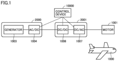
- Fig. 1 is a schematic configuration diagram illustrating a first configuration example of a power system of an aircraft.
- the aircraft is, for example, a manned or unmanned airplane, a helicopter, a drone, or the like.
- the airplane is exemplified as an aircraft 1000.
- the first configuration example of the power system includes a power source 2000, a propulsion system 2001, a propulsion system motor 1001, and a control device 10000.
- Power source 2000 generates a DC voltage.
- power source 2000 includes a generator 1003 and an AC/DC converter 1004.
- Generator 1003 generates an AC voltage.
- AC/DC converter 1004 converts the AC voltage generated by generator 1003 into a DC voltage.
- AC/DC converter 1004 supplies the generated DC voltage to propulsion system 2001.
- Propulsion system 2001 supplies a power generated by power source 2000 to propulsion system motor 1001.
- propulsion system 2001 includes a DC/DC converter 1008 and a DC/AC converter 1007.
- DC/DC converter 1008 performs voltage transformation on the DC voltage to be supplied from power source 2000.
- DC/DC converter 1008 is configured to control an input voltage to DC/AC converter 1007.
- DC/AC converter 1007 converts the transformed DC voltage into an AC voltage, and supplies the converted AC voltage to propulsion system motor 1001.
- DC/AC converter 1007 corresponds to an example of the "first power converter”.
- DC/DC converter 1008 corresponds to an example of the "second power converter”.
- Control device 10000 controls AC/DC converter 1004, DC/DC converter 1008, and DC/AC converter 1007.
- Control device 10000 is input with sensor information indicating detection values of various sensors disposed in AC/DC converter 1004, DC/DC converter 1008, and DC/AC converter 1007.
- the sensor information includes detection values of a current, a voltage, and a temperature of the each of the power converters, abnormality detection signals, and the like.
- control device 10000 may further control generator 1003 and propulsion system motor 1001.
- a plurality of control devices 10000 may be disposed in the power system, and the plurality of control devices 10000 may be configured to control power source 2000, propulsion system 2001, and propulsion system motor 1001, respectively, by exchanging the signals with each other.
- Fig. 2 is a schematic configuration diagram illustrating a second configuration example of the power system of the aircraft.
- the second configuration example of the power system has the same basic configuration as the first configuration example illustrated in Fig. 1 , but a configuration of power source 2000 is different.
- power source 2000 further includes a battery 1005 and a DC/DC converter 1006 in addition to generator 1003 and AC/DC converter 1004.
- DC/DC converter 1006 performs the voltage transformation on a DC voltage of battery 1005 and supplies the transformed voltage to propulsion system 2001.
- power source 2000 is configured to generate a DC voltage from a power generated by generator 1003 and a power of battery 1005. Note that illustration of battery 1005 and DC/DC converter 1006 is omitted in configuration examples of Fig. 3 and subsequent drawings.
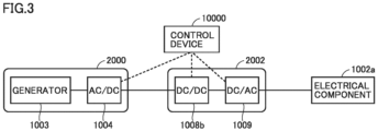
- Fig. 3 is a schematic configuration diagram illustrating a third configuration example of the power system of the aircraft.
- the third configuration example of the power system is different from the first configuration example illustrated in Fig. 1 in including an electrical component system 2002 and an electrical component 1002a instead of propulsion system 2001 and propulsion system motor 1001.
- electrical component system 2002 supplies the power generated by power source 2000 to electrical component 1002a.
- Electrical component 1002a is, for example, an electrical component driven by the AC voltage among electrical components such as a pump, an actuator, a lighting equipment, a display, and a control panel.
- electrical component system 2002 includes a DC/DC converter 1008b and a DC/AC converter 1009.
- DC/DC converter 1008b performs the voltage transformation on the DC voltage to be supplied from power source 2000.
- DC/DC converter 1008b is configured to control an input voltage to DC/AC converter 1009.
- DC/AC converter 1009 converts the transformed DC voltage into an AC voltage, and supplies the converted AC voltage to electrical component 1002a.
- Electrical component 1002a is driven by an AC voltage to be supplied from electrical component system 2002.
- DC/AC converter 1009 corresponds to an example of the "first power converter”.
- DC/DC converter 1008b corresponds to an example of the "second power converter”.
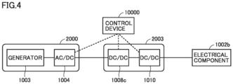
- Fig. 4 is a schematic configuration diagram illustrating a fourth configuration example of the power system of the aircraft.
- the fourth configuration example of the power system is different from the first configuration example illustrated in Fig. 1 in including an electrical component system 2003 and an electrical component 1002b instead of propulsion system 2001 and motor 1001.
- electrical component system 2003 supplies the power generated by power source 2000 to electrical component 1002b.
- Electrical component 1002b is an electrical component driven by the DC voltage among the electrical components.
- electrical component system 2003 includes a DC/DC converter 1008c and a DC/DC converter 1010.
- DC/DC converter 1008c performs the voltage transformation on the DC voltage to be supplied from power source 2000.
- DC/DC converter 1008c is configured to control an input voltage to DC/DC converter 1010.
- DC/DC converter 1010 performs the voltage transformation on the transformed DC voltage and supplies the transformed voltage to electrical component 1002b.
- Electrical component 1002b is driven by a DC voltage to be supplied from electrical component system 2003.
- DC/AC converter 1010 corresponds to an example of the "first power converter”.
- DC/DC converter 1008c corresponds to an example of the "second power converter”.
- Fig. 5 is a schematic configuration diagram illustrating a fifth configuration example of the power system of the aircraft.
- the fifth configuration example of the power system further includes electrical component systems 2002 and 2003, and electrical components 1002a and 1002b added to the first configuration example illustrated in Fig. 1 . Since electrical component systems 2002 and 2003, and electrical components 1002a and 1002b are the same as those illustrated in Figs. 3 and 4 , the description thereof will be omitted.
- power source 2000 is shared as a power supply source to propulsion system 2001 and electrical component systems 2002 and 2003.
- Propulsion system 2001, and electrical component systems 2002 and 2003 convert the DC voltage to be supplied from power source 2000 into a voltage for driving a corresponding load (propulsion system motor 1001, or electrical components 1002a and 1002b), and supply the voltage to the load.
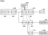
- Fig. 6 is a schematic configuration diagram illustrating a sixth configuration example of the power system of the aircraft.
- the sixth configuration example of the power system further includes DC/DC converters 1008b and 1010, DC/AC converter 1009, and electrical components 1002a and 1002b added to the configuration example illustrated in Fig. 1 . Since DC/DC converters 1008b and 1010, DC/AC converter 1009, and electrical components 1002a and 1002b are the same as those illustrated in Figs. 3 and 4 , the description thereof will be omitted.
- a DC/DC converter is shared for adjusting the input voltages of DC/AC converter 1009 and DC/DC converter 1010 in the electrical component system.
- aircraft 1000 does not include all systems 2001 to 2003, and at least one of systems 2001 to 2003 can be appropriately selected depending on the load carried by aircraft 1000.
- a battery may be further connected to a DC bus that connects the power converters.
- a circuit breaker (CB) not illustrated is arranged in each of the systems and between the systems.
- DC/DC converter 1008 of propulsion system 2001 will be described as an example.
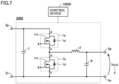
- Fig. 7 is a diagram illustrating a first circuit configuration example of DC/DC converter 1008.
- DC/DC converter 1008 includes a non-insulated step-down chopper circuit 5000.
- Non-insulated step-down chopper circuit 5000 steps down a DC voltage input from an input positive bus 3p and an input negative bus 3n, and outputs the stepped-down DC voltage as an output voltage Vout to an output positive bus 5p and an output negative bus 5n.
- Non-insulated step-down chopper circuit 5000 includes first semiconductor elements 1a and 1b as switching elements, a reactor 2, and smoothing capacitors 7 and 8.
- First semiconductor elements 1a and 1b are connected in series between input positive bus 3p and input negative bus 3n.
- First semiconductor element 1a constitutes an upper arm
- first semiconductor element 1b constitutes a lower arm.
- First semiconductor elements 1a and 1b are collectively referred to as "first semiconductor element 1".
- Reactor 2 is connected between a connection node of first semiconductor element 1a with first semiconductor element 1b and output positive bus 5p.
- Smoothing capacitor 7 is connected between input positive bus 3p and input negative bus 3n.
- Smoothing capacitor 8 is connected between output positive bus 5p and output positive bus 5n.
- step-down control on the input voltage is ideally executed by adjusting an impedance of reactor 2 and a switching duty ratio (a ratio between an on-period and an off-period) of first semiconductor element 1a (the upper arm).
- output voltage Vout may fluctuate due to influences of impedances of a wire, first semiconductor element 1, and the like, and a power converter, a load, or the like connected between output positive bus 5p and output negative bus 5n. Therefore, output voltage Vout, a current flowing through reactor 2, an inter-terminal voltage and a temperature of first semiconductor element 1, and the like are detected by a sensor (not illustrated), and detection values thereof are provided to control device 10000 as sensor information. Control device 10000 causes the sensor information to be fed back to control of a switching operation of first semiconductor element 1a.
- Fig. 8 is a diagram illustrating a configuration example of first semiconductor element 1 included in DC/DC converter 1008 illustrated in Fig. 7 .
- first semiconductor element 1 includes a metal oxide semiconductor field effect transistor (MOSFET) 1m as the switching element and a diode 1d.
- Diode 1d is a freewheeling diode (FWD), and is connected in anti-parallel with the switching element.
- diode 1d can include a parasitic diode (a body diode) of the MOSFET.
- a diode 1s may be connected to first semiconductor element 1 in anti-parallel.
- diode 1s may be one or more.
- first semiconductor element 1b (the lower arm) performs only rectification, and thus a switching function becomes unnecessary. Therefore, first semiconductor element 1b may include only the diode.
- non-insulated step-down chopper circuit 5000 may be configured by using a power semiconductor module on which the plurality of first semiconductor elements 1 are mounted in one package.
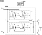
- Fig. 9 is a diagram illustrating a second circuit configuration example of DC/DC converter 1008.
- DC/DC converter 1008 includes a non-insulated step-down chopper circuit 5000b.
- Non-insulated step-down chopper circuit 5000b is different from non-insulated step-down chopper circuit 5000 illustrated in Fig. 7 in that each of the upper arm and the lower arm includes the plurality of first semiconductor elements 1 connected in parallel.
- each of the upper arm and the lower arm includes a first power semiconductor module 6 having two first semiconductor elements 1 connected in parallel. Note that the number of first semiconductor elements 1 included in first power semiconductor module 6 may be greater than or equal to three.
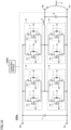
- Fig. 10 is a diagram illustrating a third circuit configuration example of DC/DC converter 1008.
- DC/DC converter 1008 includes a non-insulated step-down chopper circuit 5000c.
- Non-insulated step-down chopper circuit 5000c is different from non-insulated step-down chopper circuit 5000 illustrated in Fig. 7 in that the each of the upper arm and the lower arm includes a plurality of first power semiconductor modules 6 connected in parallel.
- the each of the upper arm and the lower arm includes two first power semiconductor modules 6 connected in parallel.
- Each of first power semiconductor modules 6 includes the two first semiconductor elements 1 connected in parallel. Note that both the number of first power semiconductor modules 6 included in the each of the arms and the number of first semiconductor elements 1 included in the each of first power semiconductor modules 6 may be greater than or equal to three.
- DC/DC conversion circuit 1008 may include a non-insulated chopper circuit having a full bridge circuit.
- an isolated step-down chopper circuit using a transformer or a capacitor may be adopted.
- the non-insulated step-down chopper circuit is exemplified as DC/DC conversion circuit 1008 being a step-down circuit.
- DC/DC conversion circuit 1008 is a step-up circuit
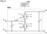
- a non-insulated step-up chopper circuit as illustrated in Fig. 11 can be adopted.
- Fig. 11 is a diagram illustrating a fourth circuit configuration example of DC/DC converter 1008.
- DC/DC converter 1008 includes a non-insulated step-up chopper circuit 5000d.
- Non-insulated step-up chopper circuit 5000d is different from non-insulated step-down chopper circuit 5000 illustrated in Fig. 7 in that reactor 2 is connected between input positive bus 3p and the connection node of first semiconductor element 1a with first semiconductor element 1b.
- step-up control on the input voltage is ideally executed by adjusting the impedance of reactor 2 and a switching duty ratio of first semiconductor element 1b (the lower arm).
- control device 10000 causes the sensor information to be fed back to control of a switching operation of first semiconductor element 1b.
- DC/AC converter 1007 of propulsion system 2001 will be described as an example.
- Fig. 12 is a diagram illustrating a first circuit configuration example of DC/AC converter 1007.
- DC/AC converter 1007 includes a three-phase two-level inverter circuit 5001.
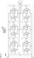
- Three-phase two-level inverter circuit 5001 converts DC voltages input from an input positive bus 9p and an input negative bus 9n into three-phase (U-phase, V-phase, W-phase) AC voltages, and outputs the three-phase AC voltages to AC output terminals 1 1u, 1 1v, and 1 1w.
- Three-phase two-level inverter circuit 5001 includes second semiconductor elements 10a to 10f as switching elements and a smoothing capacitor 13.
- Second semiconductor elements 10a and 10b are connected in series between input positive bus 9p and input negative bus 9n.
- a connection node of second semiconductor element 10a with second semiconductor element 10b is connected to U-phase output terminal 1 1u.
- Second semiconductor elements 10c and 10d are connected in series between input positive bus 9p and input negative bus 9n.
- a connection node of second semiconductor element 10c with second semiconductor element 10d is connected to V-phase output terminal 11v.
- Second semiconductor elements 10e and 10f are connected in series between input positive bus 9p and input negative bus 9n.
- a connection node of second semiconductor element 10e with second semiconductor element 10f is connected to W-phase output terminal 11w.
- Second semiconductor elements 10a and 10b constitute a U-phase leg
- second semiconductor elements 10c and 10d constitute a V-phase leg
- second semiconductor elements 10e and 10f constitute a W-phase leg.
- Second semiconductor elements 10a to 10f are collectively referred to as "second semiconductor elements 10".
- Smoothing capacitor 13 is connected between input positive bus 9p and input negative bus 9n, and smooths the DC voltage including the ripple voltage.
- Three-phase two-level inverter circuit 5001 is equipped with a sensor (not illustrated) for detecting a current flowing through U-phase output terminal 11u, V-phase output terminal 1 1v, and W-phase output terminal 11w, a voltage across U-phase output terminal 11u, V-phase output terminal 1 1v, and W-phase output terminal 11w, and an inter-terminal voltage and a temperature of each of second semiconductor elements 10. Detection values thereof from the sensor are given to control device 10000 as the sensor information. Control device 10000 causes the sensor information to be fed back to control of a switching operation of the each of second semiconductor elements 10.
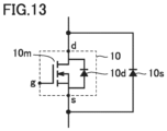
- Fig. 13 is a diagram illustrating a configuration example of second semiconductor element 10 included in DC/AC converter 1007 illustrated in Fig. 12 .
- second semiconductor element 10 includes a MOSFET 10m as the switching element and a diode 10d.
- Diode 10d is the freewheeling diode and is connected in anti-parallel with the switching element.
- diode 10d can include the parasitic diode of the MOSFET.
- a diode 10s may be connected to second semiconductor element 10 in anti-parallel.
- diode 10s may be one or more.
- three-phase two-level inverter circuit 5001 may be configured by using the power semiconductor module on which the plurality of second semiconductor elements 10 are mounted in one package.
- Fig. 14 is a diagram illustrating a second circuit configuration example of DC/AC converter 1007.
- DC/AC converter 1007 includes a three-phase two-level inverter circuit 5001b.
- Three-phase two-level inverter circuit 5001b is different from three-phase two-level inverter circuit 5001 illustrated in Fig. 12 in that the each of the upper arm and the lower arm includes the plurality of second semiconductor elements 10 connected in parallel.
- each of the upper arm and the lower arm includes a second power semiconductor module 14 having two second semiconductor elements 10 connected in parallel.
- the number of second semiconductor elements 10 included in second power semiconductor module 14 may be greater than or equal to three.
- Fig. 15 is a diagram illustrating a third circuit configuration example of DC/AC converter 1007.
- DC/AC converter 1007 includes a three-phase two-level inverter circuit 5001c.
- Three-phase two-level inverter circuit 5001c is different from three-phase two-level inverter circuit 5001 illustrated in Fig. 12 in that the each of the upper arm and the lower arm includes the plurality of second power semiconductor modules 14 connected in parallel.
- each of the upper arm and the lower arm includes two second power semiconductor modules 14 connected in parallel.
- each of second power semiconductor modules 14 includes the plurality of second semiconductor elements 10 connected in parallel. Note that the number of second power semiconductor modules 14 included in the each of the arms may greater than or equal to 3.
- three-phase two-level inverter circuits 5001, 5001b, and 5001c may be configured by using discrete semiconductor elements.
- DC/AC converter 1007 is only required to have a DC/AC conversion function, and is not limited to the three-phase two-level inverter circuit.
- DC/AC converter 1007 may be a multi-level circuit, for example, a three-phase three-level inverter circuit, a three-phase five-level inverter circuit, a three-phase gradation inverter circuit, or the like.
- DC/DC converters 1008b, 1008c, and 1010 can have a circuit configuration similar to that of DC/DC converter 1008.
- DC/AC converter 1009 can have a circuit configuration similar to that of DC/AC converter 1007.
- a rated voltage, a rated current, and the like of the each of the semiconductor elements constituting a respective power converter are different depending on a capacity of the load.
- each of semiconductor elements 1 and 10 a configuration example in which the MOSFET is adopted as the switching element, the parasitic diode of the MOSFET is used as the freewheeling diode, or the freewheeling diode is connected in anti-parallel to the switching element has been described.
- a silicon (Si)-MOSFET, a silicon carbide (SiC)-MOSFET, a Si-insulated gate bipolar transistor (Si-IGBT), a SiC-IGBT, a GaN-high electron mobility transistor (GaN-HEMT), or the like can be used as the switching element.
- a Si-diode, a SiC-diode, a SiC-Schottky barrier diode (SiC-SBD), or the like can be used as the freewheeling diode.
- the IGBT is used as the switching element, it is always necessary to connect the freewheeling diode in anti-parallel to the switching element.
- the RC-IGBT is used as the switching element, it is not necessary to connect the freewheeling diode to the switching element.
- first power semiconductor module 6 will be described as an example.
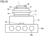
- Fig. 16 is a schematic configuration diagram of first power semiconductor module 6. As illustrated in Fig. 16 , first power semiconductor module 6 includes first semiconductor element 1, bonding materials 17 and 21, a front electrode 20, an insulating material 19, a back electrode 18, a base plate 16, and a water-cooling device 23a.
- First semiconductor element 1 is bonded to front electrode 20 with bonding material 21.
- Bonding materials 17 and 21 are, for example, a paste made of silver (Ag) or copper (Cu), a solder, or the like.
- Front electrode 20 and back electrode 18 are made of Cu, aluminum (Al), or the like.
- Front electrode 20 and back electrode 18 are attached to insulating material 19 with a brazing material or the like.
- Insulating material 19 is made of silicon nitride (Si 3 N 4 ), alumina (Al 2 O 3 ), aluminum nitride (AlN), a resin material, or the like.
- Base plate 16 is made of aluminum-silicon carbide (Al-SiC), magnesium-silicon carbide Mg-SiC), Al, Cu, an Al alloy, a Cu alloy, or the like.
- Base plate 16 is bonded to water-cooling device 23a by a screw, caulking, or the like. Water-cooling device 23a is formed with a cooling pipe 23b.
- water-cooling device 23a is exemplified as a cooling device, but an air-cooling device including fins may be used.
- grease or a heat spreader for diffusing heat radiation may be interposed between base plate 16 and water-cooling device 23a.
- the configuration of the power semiconductor module is not limited to the example of Fig. 16 , and a configuration in which base plate 16 is directly bonded to water-cooling device 23a, a configuration in which cooling is performed from both surfaces of first semiconductor element 1, or the like can be adopted.
- Fig. 17 is a diagram illustrating a mechanism for generating neutrons that may cause the accidental failure of the semiconductor element.
- cosmic rays 30 exist in a space 27 and constantly falls on the earth.
- cosmic rays 30 collide with the atmosphere to generate neutrons 31.
- Neutrons 31 may collide with second semiconductor element 10 mounted on the aircraft operating on a ground surface 29 or flying in the sky.
- second semiconductor element 10 may fail due to the collision with neutrons 31.
- SEB single event burnout
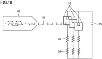
- FIG. 18 is a diagram illustrating an experimental example of the failure rate of the semiconductor element.
- the plurality of (for example, three) second semiconductor elements 10 are connected in parallel between a positive electrode and a negative electrode of a DC power source 33.
- a voltage-dividing resistor 35 and a leakage-measuring resistor 36 are connected in series with the each of second semiconductor elements 10 between the positive electrode and the negative electrode of DC power source 33.
- DC power source 33 is electrically connected between a drain and a source of the MOSFET.
- a DC voltage of DC power source 33 is divided by second semiconductor elements 10, voltage-dividing resistor 35, and resistor 36.
- a drain-source resistance of the each of second semiconductor element 10, voltage-dividing resistor 35, and resistor 36 has a relationship in which a resistance value of resistor 36 is sufficiently smaller than a resistance value of voltage-dividing resistor 35, and the resistance value of voltage-dividing resistor 35 is sufficiently smaller than a resistance value of the drain-source resistance of the each of second semiconductor elements 10. Therefore, most of the DC voltage of DC power source 33 is applied to second semiconductor element 10.
- the most of the DC voltage of DC power source 33 is applied to voltage-dividing resistor 35.
- An inter-terminal voltage of resistor 36 is detected by a data logger (not illustrated).
- a leakage current can be calculated from a detection value of the inter-terminal voltage of resistor 36 and the resistance value of resistor 36. In a case where second semiconductor elements 10 are normal, the leakage current is small, and the leakage current increases due to the failures of second semiconductor elements 10.
- second semiconductor elements 10 are irradiated with neutrons 31 from an accelerator 32 in a state where the DC voltage is applied to second semiconductor elements 10 from DC power source 33.
- the SEB stochastically occurs, and second semiconductor elements 10 fail.
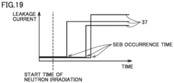
- Fig. 19 is a diagram illustrating variation of leakage current during irradiation with neutrons 31.
- Fig. 19 illustrates waveforms 37 of three leakage currents.
- Three waveforms 37 represent the leakage current flowing through each of three second semiconductor elements 10 illustrated in Fig. 18 .
- a failure rate of the each of second semiconductor elements 10 can be calculated from a total number of second semiconductor elements 10 used in the experiment, a time at which the each of second semiconductor elements 10 fails, and the number of second semiconductor elements 10 failed. Note that the failure rate is generally calculated by using an index called the "Failure-in-Time (FIT)".
- the FIT is a unit representing the failure rate, and represents the number of the second semiconductor elements failing within the ninth power of ten hours. For example, "1 FIT" means a probability that one failure occurs within the ninth power of ten hours. A lower FIT indicates a lower failure rate.
- the number of the neutrons with which the irradiation is performed per unit time and per unit area is larger than the number of the neutrons actually falling on the natural world per unit time and per unit area. Therefore, the experiment is substantially an accelerated test. Accordingly, the FIT under an environment in which second semiconductor elements 10 are placed is corrected by using the number of the neutrons per unit time and per unit area under the environment.
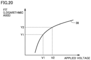
- Fig. 20 is a diagram illustrating a relationship between a voltage applied to second semiconductor element 10 and a FIT of one second semiconductor element 10.
- a horizontal axis represents an applied voltage
- a vertical axis represents the FIT.
- Fig. 20 illustrates a FIT curve 38 of second semiconductor element 10.
- the FIT when a voltage V1 is applied is Y1
- the FIT when a voltage V2 is applied is Y2. If V1 ⁇ V2, then Y1 ⁇ Y2. Accordingly, it can be seen that the FIT of second semiconductor element 10 can be controlled by adjusting the voltage applied to second semiconductor element 10.
- FIT is correlated with the withstand voltage of the semiconductor element, and it is known that the FIT decreases as the withstand voltage of the semiconductor element increases.
- Fig. 21 is a diagram illustrating the correlation between a withstand voltage and the FIT of the semiconductor element.
- Fig. 21 illustrates first FIT curve 38 indicating the relationship between the applied voltage and the FIT of second semiconductor element 10, and a second FIT curve 40 indicating a relationship between an applied voltage and a FIT of a high withstand-voltage semiconductor element 39 having a higher withstand voltage than second semiconductor element 10.
- first FIT curve 38 Comparing first FIT curve 38 with second FIT curve 40, the FIT of second semiconductor element 10 becomes Y1 when voltage V1 is applied, whereas the FIT of high withstand-voltage semiconductor element 39 becomes W1 lower than Y1. Note that the correlation between the withstand voltage and the FIT of the semiconductor element illustrated in Fig. 21 remains unchanged regardless of a height at which the semiconductor element is placed.
- second semiconductor element 10 and high withstand-voltage semiconductor element 39 in Fig. 21 are both the MOSFETs and have an equal element area.
- a difference between second semiconductor element 10 and high withstand-voltage semiconductor element 39 is only a thickness or a concentration of a drift layer that holds the withstand voltage of the MOSFET.
- first FIT curve 38 and second FIT curve 40 may intersect or a vertical relationship may be reversed.
- first FIT curve 38 and second FIT curve 40 may intersect or the vertical relationship may be reversed. Assuming these cases, the relationship between the applied voltage and the FIT of the semiconductor element should be confirmed by acquiring the FIT curves by performing the experiment described above (see Fig. 19 ) for the each of the semiconductor elements.
- FIT is also correlated with the temperature (the junction temperature) of the semiconductor element, and the FIT tends to decrease as the junction temperature increases.
- Fig. 22 is a diagram illustrating a correlation between a junction temperature and the FIT of second semiconductor element 10.
- Fig. 22 illustrates FIT curves 41 to 43 indicating a relationship between the junction temperature and the FIT of second semiconductor element 10.
- a third FIT curve 41 is a FIT curve when the junction temperature is A [°C].
- a fourth FIT curve 42 is a FIT curve when the junction temperature is B [°C].
- a fifth FIT curve 43 is a FIT curve when the junction temperature is C [°C]. Note that A [°C] ⁇ B [°C] ⁇ C [°C].
- the FIT in a case where voltage V1 is applied to second semiconductor element 10, the FIT is YA when the junction temperature is A [°C], the FIT is YB when the junction temperature is B [°C], and the FIT is YC when the junction temperature is C [°C]. Note that YC ⁇ YB ⁇ YA.
- the withstand voltage increases as the junction temperature of the semiconductor element increases, and the withstand voltage decreases as the junction temperature decreases. Therefore, in Fig. 22 , the withstand voltage increases as the junction temperature increases, and thus the FIT decreases. On the contrary, the withstand voltage decreases as the junction temperature decreases, and thus the FIT increases.
- the correlation between the junction temperature and the FIT of the semiconductor element remains unchanged regardless of a height of a place where the semiconductor element is located.
- the correlation between the junction temperature and the FIT is not necessarily proportional, the relationship between the applied voltage and the FIT of the each of the semiconductor elements should be confirmed by changing the junction temperature and acquiring the FIT curve depending on the junction temperature for the each of the semiconductor elements in the experiment described above (see Fig. 19 ).
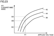
- Fig. 23 is a diagram illustrating a FIT of each of second semiconductor element 10, second power semiconductor module 14, and three-phase two-level inverter circuit 5001.
- first FIT curve 38 is a FIT curve of one second semiconductor element 10.
- a sixth FIT curve 44 is a FIT curve of one second power semiconductor module 14.
- a seventh FIT curve 45 is a FIT curve of one three-phase two-level inverter circuit 5001.
- the FIT of second power semiconductor module 14 on which the plurality of second semiconductor elements 10 are mounted increases in proportion to the number of second semiconductor elements 10 mounted.
- sixth FIT curve 44 of one second power semiconductor module 14 is calculated by the following expression (1) with first FIT curve 38 of one second semiconductor element 10.
- Sixth FIT curve 44 first FIT curve 38 ⁇ number of second semiconductor elements 10 mounted
- both seventh FIT curve 45 and sixth FIT curve 44 are the FIT curves at the height of 0 m above sea level.
- first FIT curve 38, sixth FIT curve 44, and seventh FIT curve 45 have a relationship as illustrated in Fig. 23 .
- the FIT of second semiconductor element 10 of XC, the FIT of second power semiconductor module 14 of XB, and the FIT of three-phase two-level inverter circuit 5001 of XA has a relationship of XC ⁇ XB ⁇ XA.
- seventh FIT curve 45 of three-phase two-level inverter circuit 5001 is calculated on the basis of first FIT curve 38 of one second semiconductor element 10.
- the FIT of each of DC/DC converters 1008, 1008b, 1008c and 1010, and DC/AC converters 1007 and 1009 can be calculated by using the FIT curves of the semiconductor elements mounted on the power converter.
- the number of the neutrons per unit time and unit area [number/(time or area)] varies depending on the height, the latitude, and the longitude of the place where the neutrons are located. In the following description, the number of the neutrons per unit time and unit area is also simply referred to as "number of the neutrons". The number of the neutrons corresponds to the amount of the neutrons.
- Spectra of the neutrons depending on the height, the latitude, and the longitude can be calculated by using, for example, an EXPACS (excel-based program for calculating atomic cosmic-ray spectrum).
- the EXPACS refers to a program capable of calculating a cosmic ray flux and energy thereof at any place and time in the atmosphere.
- the spectra of the neutrons refer to data representing the number of the neutrons present for a wide energy band of the neutrons per unit time and unit area. From the spectra of the neutrons obtained by the EXPACS, it is possible to acquire data indicating the dependency of the number of the neutrons having any energy on the height, the latitude, and the longitude.
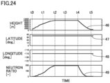
- Fig. 24 is a diagram illustrating a first example of a neutron ratio 49 calculated on the basis of height data 46, latitude data 47, and longitude data 48 when the aircraft flies on an optional date.
- the "neutron ratio” means a ratio of the number of the neutrons per unit time and unit area calculated from the height, the latitude, and the longitude to the number of the neutrons per unit time and unit area at the place of 0 m above sea level on arbitrary coordinates.
- a time t0 indicates a time before takeoff of the aircraft
- a time t1 indicates a time when the height increases
- a time t2 indicates a time when the height reaches a maximum height
- a time t3 indicates a time when the aircraft is flying at the maximum height
- a time t4 indicates a time before the height decreases
- a time t5 indicates a time after landing.
- height data 46 indicating a height of the aircraft varies in a range of 0 to 12000 [m].
- each of latitude data 47 indicating a latitude of the aircraft and longitude data 48 indicating a longitude of the aircraft is constant.
- Neutron ratio 49 is calculated on the basis of the number of the neutrons calculated from height data 46, latitude data 47, and longitude data 48 at each of the times. It can be seen from Fig. 24 that neutron ratio 49 varies within a range of 0 to 200 following the variation of height data 46. Note that as the number of the neutrons increases, neutron ratio 49 increases. Accordingly, neutron ratio 49 varies greatly depending on the height of the aircraft.
- Fig. 25 is a diagram illustrating a second example of neutron ratio 49 calculated on the basis of height data 46, latitude data 47, and longitude data 48 when the aircraft flies on the optional date.
- the second example illustrated in Fig. 25 is different from the first example illustrated in Fig. 24 in that latitude data 47 and longitude data 48 vary in addition to height data 46.
- neutron ratio 49 varies within a range of 0 to 200 following not only the variation of height data 46, but also the variations of latitude data 47 and longitude data 48. Accordingly, neutron ratio 49 greatly varies depending on the height, the latitude, and the longitude of the aircraft.
- Neutron ratio 49 is directly linked to the failure rate of the each of the semiconductor elements.
- a relationship between neutron ratio 49 and the failure rate will be described by taking three-phase two-level inverter circuit 5001 as an example.
- Expression (2) indicating seventh FIT curve 45 of three-phase two-level inverter circuit 5001 can be transformed as in Expression (3) in consideration of neutron ratio 49.
- Seventh FIT curve 45 sixth FIT curve 44 ⁇ number of second power semiconductor modules 14 mounted x neutron ratio 49
- sixth FIT curve 44 is the FIT curve at the height of 0 m above sea level.
- Fig. 26 is a diagram illustrating a correlation between the FIT of three-phase two-level inverter circuit 5001 and neutron ratio 49.
- an eighth FIT curve 51 is a FIT curve of one three-phase two-level inverter circuit 5001 when neutron ratio 49 is a first value.
- a ninth FIT curve 52 is a FIT curve of one three-phase two-level inverter circuit 5001 when neutron ratio 49 is a second value larger than the first value.
- the FIT in a case where an input voltage 50 to three-phase two-level inverter circuit 5001 is Va, the FIT is ZA when neutron ratio 49 is the second value, and the FIT is ZB when neutron ratio 49 is the first value. Note that ZB ⁇ ZA. In other words, in case where the input voltages are equal, the FIT of three-phase two-level inverter circuit 5001 increases as neutron ratio 49 increases.
- Fig. 27 is a diagram illustrating a first example of neutron ratio 49 when the aircraft flies on the optional date, and first FIT data 53 and input voltage 50 of three-phase two-level inverter circuit 5001. Note that neutron ratio 49 illustrated in Fig. 27 is calculated on the basis of height data 46, latitude data 47, and longitude data 48 illustrated in Fig. 25 . First FIT data 53 is calculated by using neutron ratio 49 and expression (3).
- input voltage 50 to three-phase two-level inverter circuit 5001 indicates a voltage applied between input positive bus 9p and input negative bus 9n of three-phase two-level inverter circuit 5001, and is maintained at a constant voltage Va.
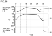
- Fig. 28 is a diagram illustrating a second example of neutron ratio 49 when the aircraft flies on the optional date, and second FIT data 54 and input voltage 50 of three-phase two-level inverter circuit 5001. Note that neutron ratio 49 illustrated in Fig. 28 is calculated on the basis of height data 46, latitude data 47, and longitude data 48 illustrated in Fig. 26 . Second FIT data 54 is calculated by using neutron ratio 49 and expression (3).
- input voltage 50 to three-phase two-level inverter circuit 5001 indicates a voltage applied between input positive bus 9p and input negative bus 9n of three-phase two-level inverter circuit 5001, and is maintained at the constant voltage Va.
- first FIT data 53 and second FIT data 54 also vary following the variation of neutron ratio 49.
- the FIT increases as neutron ratio 49 increases, and the FIT decreases as neutron ratio 49 decreases.
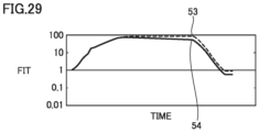
- Fig. 29 is a diagram illustrating comparison between first FIT data 53 and second FIT data 54. As illustrated in Fig. 29 , the variation of the FIT of three-phase two-level inverter circuit 5001 can be obtained more accurately in a case where height data 46, latitude data 47, and longitude data 48 are considered, as opposed to a case where only height data 46 is considered.
- neutron ratio 49 is calculated by using height data 46, latitude data 47, and longitude data 48 of the route, and input voltage 50 of three-phase two-level inverter circuit 5001 is adjusted on the basis of the calculated neutron ratio 49.
- Fig. 30 is a diagram illustrating an example of adjustment of the input voltage of three-phase two-level inverter circuit 5001.
- Fig. 30 is similar to Fig. 28 with third FIT data 56 and an input voltage 55 added.
- third FIT data 56 indicates a variation of the FIT when neutron ratio 49 varies under input voltage 55 being a constant voltage Vb.
- third FIT data 56 is suppressed to less than or equal to1 FIT while the aircraft is in flight. Accordingly, the reliability of three-phase two-level inverter circuit 5001 against the SEB is ensured while the aircraft is in flight.
- the input voltage of DC/AC converter 1007 included in propulsion system 2001 is adjusted depending on neutron ratio 49 calculated from height data 46, latitude data 47, and longitude data 48 of the route. In other words, an output voltage of DC/DC converter 1008 is adjusted.
- the input voltage of DC/AC converter 1009 included in electrical component system 2002 is adjusted depending on neutron ratio 49. In other words, an output voltage of DC/DC converter 1008b is adjusted.
- the input voltage of DC/DC converter 1010 included in the electrical component system 2003 is adjusted depending on neutron ratio 49. In other words, an output voltage of DC/DC converter 1008c is adjusted.
- the input voltage of the each of the power converters can be determined in advance from height data 46, latitude data 47, and longitude data 48 of the route as illustrated in Fig. 28 .
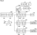
- Fig. 31 is a diagram illustrating a configuration example of the power system having a function of adjusting the input voltages of the power converters.
- the configuration example of the power system illustrated in Fig. 31 is similar to the fifth configuration example of the power system illustrated in Fig. 5 with a global positioning system (GPS) 61 and an altimeter 62 added.
- GPS global positioning system
- GPS 61 measures a latitude and a longitude of a current position of aircraft 1000 while aircraft 1000 is in flight, and outputs measured values thereof to control device 10000.
- Altimeter 62 measures a height of the current position of aircraft 1000, and outputs a measured value thereof to control device 10000. Note that in a case where the height of aircraft 1000 can be calculated from the measured values of GPS 61, altimeter 62 is unnecessary.
- Fig. 32 is a diagram illustrating a hardware configuration of control device 10000.
- control device 10000 includes a central processing unit (CPU) 70, a random access memory (RAM) 71, a read only memory (ROM) 72, an interface (I/F) device 73, and a storage device 74.
- CPU 70, RAM 71, ROM 72, I/F device 73, and storage device 74 exchange various data through a communication bus 75.
- CPU 70 develops a program stored in ROM 72 in RAM 71, and executes the program. A process executed by control device 10000 is described in the program stored in ROM 72.
- I/F device 73 receives measurement data of various measured values including those of GPS 61 and altimeter 62. In addition, I/F device 73 transmits a control signal for controlling the each of the power converters to the each of the power converters.
- Storage device 74 is a storage that stores various types of information, and stores information on the each of the power converters.
- the information on the each of the power converters includes information on the power semiconductor modules and the semiconductor elements constituting the each of the power converters.
- storage device 74 stores information relative to the failure rates of the power converters, the power semiconductor modules, and the semiconductor elements.
- the information relative to the failure rates includes information relative to the FIT curves illustrated in Figs. 20 to 23 .
- Storage device 74 is, for example, a hard disk drive (HDD) or a solid state drive (SSD).
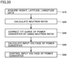
- Fig. 33 is a flowchart illustrating an example of a procedure of a process of determining the input voltage of each of the power converters of the power system. A series of processes illustrated in this flowchart is executed by control device 10000 at each predetermined cycle while aircraft 1000 is in flight.
- control device 10000 acquires measurement data of the height of aircraft 1000 measured by altimeter 62, and acquires measurement data of the latitude and the longitude of the current position of aircraft 1000 measured by GPS 61 (step S10).
- control device 10000 calculates the neutron ratio at the current position of aircraft 1000 by using the measurement data of the height, the latitude, and the longitude of aircraft 1000 (step S20).
- control device 10000 calculates the number of the neutrons at the current position of aircraft 1000 based on the acquired measurement data of the height, the latitude, and the longitude.
- computer 63 calculates a ratio of the number of the neutrons at the current position of aircraft 1000 to the number of the neutrons at the place of 0 m above sea level as the neutron ratio.
- control device 10000 corrects a FIT curve acquired in advance by using the calculated neutron ratio for the each of the power converters (step S30).
- control device 10000 corrects the FIT curve by substituting the neutron ratio calculated in S20 into expression (3) described above for the each of the power converters.
- control device 10000 calculates the input voltage by using the corrected FIT curve for the each of the power converters (step S40). In S40, control device 10000 calculates the input voltage at which the FIT can satisfy the safety design value (for example, less than or equal to 1 FIT) from the corrected FIT curve.
- the safety design value for example, less than or equal to 1 FIT
- control device 10000 sets the calculated input voltage as a target value, and adjusts the input voltage of the each of the power converters to be the target value (step S50). For example, control device 10000 controls the output voltage of DC/DC converter 1008 to make the input voltage of DC/AC converter 1007 included in propulsion system 2001 be the target value.
- Fig. 34 is a flowchart illustrating another example of the procedure of the process of determining the input voltage of the each of the power converters of the power system. The series of processes illustrated in this flowchart is executed by control device 10000 at the each predetermined cycle while aircraft 1000 is in flight.
- control device 10000 Upon acquiring the measurement data of the height, the latitude, and the longitude of aircraft 1000 in S 10, control device 10000 calculates the input voltage based on the measurement data by referring to a map created in advance for the each of the power converters (step S60).
- the map defines a relationship among the height, the longitude, the latitude and the input voltage of the each of the power converters.
- the map can be created by correcting the FIT curve by using the neutron ratio calculated from the height, the longitude, and the latitude, and obtaining the input voltage at which the FIT satisfies the safety design value in the corrected FIT curve.
- the map is created in advance, and stored in storage device 74 (see Fig. 32 ) of control device 10000.
- Control device 10000 sets the calculated input voltage as a target value, and adjusts the input voltage of the each of the power converters to be the target value (step S50).
- Fig. 35 is a diagram illustrating an example of transition of the FIT when an input voltage of DC/AC converter 1007 of propulsion system 2001 is adjusted.
- the adjustment of the input voltage of DC/AC converter 1007 illustrated in Fig. 35 is implemented by controlling the output voltage of DC/DC converter 1008.
- Fig. 35 illustrates neutron ratio 49 calculated on the basis of height data 46, latitude data 47, and longitude data 48 illustrated in Fig. 25 , and second FIT data 54 calculated by using neutron ratio 49 and input voltage 50 (the constant voltage Va).
- Fig. 35 further illustrates third FIT data 56 calculated by using neutron ratio 49 and input voltage 55 (the constant voltage Vb).
- control device 10000 calculates the neutron ratio by using the measurement data of the height, the latitude, and the longitude of aircraft 1000 for each predetermined control cycle. Then, computer 63 corrects the FIT curve of DC/AC converter 1007 acquired in advance by using the calculated neutron ratio in S30 of Fig. 33 . In S30, control device 10000 corrects the FIT curve of DC/AC converter 1007 by substituting the neutron ratio calculated in S20 into expression (3) described above. Accordingly, a correlation between the input voltage and the FIT of DC/AC converter 1007 is obtained.
- control device 10000 calculates the input voltage when the FIT becomes the safety design value (less than or equal to 1 FIT) by using the corrected FIT curve.
- Control device 10000 controls the output voltage of DC/DC converter 1008 to be matched with the calculated input voltage in S50 of Fig. 33 .
- Fig. 35 illustrates an input voltage 57 of DC/AC converter 1007 fluctuating in response to control of DC/DC converter 1008 and fourth FIT data 58 of DC/AC converter 1007 corresponding to input voltage 57.
- Input voltage 57 of DC/AC converter 1007 varies depending on fluctuation of neutron ratio 49. Specifically, as neutron ratio 49 increases, input voltage 57 decreases.
- fourth FIT data 58 transitions around an upper limit value of the safety design value (less than or equal to 1 FIT) while aircraft 1000 is in flight.
- the input voltage of DC/AC converter 10007 is adjusted by using the FIT curve based on the neutron ratio calculated from the height, the latitude, and the longitude of aircraft 1000, whereby reliability of DC/AC converter 1007 against the SEB can be secured while aircraft 1000 is in flight.
- Propulsion system motor 1001 of aircraft 1000 generally require a high output when aircraft 1000 ascends the height from the takeoff, and descends the height to land.
- an output of propulsion system motor 1001 may be lower than that when the aircraft ascends the height and when the aircraft descends the height. Since there is a correlation between the output of the motor and an input voltage of the motor, the output of propulsion system motor 1001 decreases when the input voltage of propulsion system motor 1001 is low. Accordingly, when aircraft 1000 ascends the height from the takeoff and when aircraft 1000 descends the height to land, the input voltage of propulsion system motor 1001 is desirably higher than that after the aircraft ascends the height.
- Transition of input voltage 57 illustrated in Fig. 35 also corresponds to such load condition of aircraft 1000. Accordingly, during a period when the neutron ratio decreases, that is, when aircraft 1000 ascends the height and descends the height, input voltage 57 of DC/AC converter 1007 can be set to a high voltage to ensure a necessary motor output.
- the input voltages of corresponding DC/AC converter 1009 and DC/DC converter 1010 may be determined in advance before aircraft 1000 is in flight, and the input voltage may be maintained at the determined voltage during the flight.
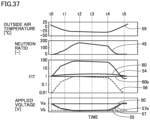
- Fig. 36 is a diagram illustrating an example of transition of the FIT according to transition of an outside air temperature 59 while aircraft 1000 is in flight.
- Fig. 36 assumes a case where a temperature of second semiconductor element 10 constituting DC/AC converter 1007 transitions at the same temperature as outside air temperature 59 during adjustment of input voltage 57 illustrated in Fig. 35 .
- Fig. 36 further illustrates fifth FIT data 60 of DC/AC converter 1007.
- FIT data 60 it can be seen that the FIT of DC/AC converter 1007 increases as outside air temperature 59 decreases while aircraft 1000 is in flight and the temperature of second semiconductor element 10 decreases. This is because, as illustrated in Fig. 22 , the withstand voltage of the semiconductor element decreases as the temperature of the semiconductor element decreases, and thus the FIT increases.
- the safety design value is set to less than or equal to 1 FIT, the FIT exceeds the safety design value depending on the decrease in outside air temperature 59, and thus the reliability against the SEB of DC/AC converter 1007 cannot be secured.
- Fig. 37 is a diagram illustrating an example of transition of the FIT when the input voltage of DC/AC converter 1007 is adjusted depending on outside air temperature 59 in propulsion system 2001.
- Fig. 37 illustrates an input voltage 57b of DC/AC converter 1007 adjusted depending on transition of outside air temperature 59 and fifth FIT data 60b of DC/AC converter 1007 with respect to transition of input voltage 57b.
- the fifth FIT data 60b transitions around the upper limit value of the safety design value (less than or equal to 1 FIT) while aircraft 1000 is in flight similarly to fourth FIT data 58. Accordingly, it possible to ensure the reliability of DC/AC converter 1007 against the SEB while aircraft 1000 is in flight.
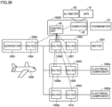
- Fig. 38 is a diagram illustrating a configuration example of a power system according to a second embodiment.
- the configuration example of the power system illustrated in Fig. 38 is similar to the configuration example of the power system illustrated in Fig. 31 with a thermometer 67 added.
- Thermometer 67 measures the temperature of the each of the power converters while aircraft 1000 is in flight, and outputs a measured value thereof to control device 10000.
- Control device 10000 determines the input voltage of the each of the power converters based on the measured values input from GPS 61, altimeter 62, and thermometer 67.
- Fig. 39 is a flowchart illustrating an example of the procedure of the process of determining the input voltage of the each of the power converters of the power system. A series of processes illustrated in this flowchart is executed by control device 10000 at each predetermined control cycle while aircraft 1000 is in flight.
- S30 is replaced with S70
- S40 is replaced with S80, which are in the flowchart illustrated in Fig. 33 .
- control device 10000 acquires the measurement data of the height of aircraft 1000 measured by altimeter 62, and acquires the measurement data of the latitude and the longitude of the current position of aircraft 1000 measured by GPS 61 (step S10).
- control device 10000 calculates the neutron ratio by using the measurement data of the height, the latitude, and the longitude of aircraft 1000 (step S20).
- control device 10000 calculates the number of the neutrons at the current position of aircraft 1000 based on the acquired measurement data of the height, the latitude, and the longitude. Then, control device 10000 calculates the ratio of the number of the neutrons at the current position of aircraft 1000 to the number of the neutrons at the place of 0 m above sea level as the neutron ratio.
- control device 10000 acquires temperature information on the each of the power converters measured by thermometer 67 (step S70).
- Control device 10000 corrects the FIT curve acquired in advance for the each of the power converters by using the neutron ratio calculated in S20 and the temperature information acquired in S30 (step S80). In S80, control device 10000 corrects the FIT curve by substituting the neutron ratio calculated in S20 into expression (3) described above. Further, control device 10000 corrects the FIT curve by using the temperature information acquired in S70.
- control device 10000 calculates the input voltage by using the corrected FIT curve for the each of the power converters (step S40). In S40, control device 10000 calculates the input voltage at which the FIT can satisfy the safety design value (for example, less than or equal to 1 FIT) from the corrected FIT curve.
- the safety design value for example, less than or equal to 1 FIT
- control device 10000 sets the input voltage calculated in S40 as a target value, and adjusts the input voltage of the each of the power converters to be the target value. For example, control device 10000 controls the output voltage of DC/DC converter 1008 to make the input voltage of DC/AC converter 1007 included in propulsion system 2001 be the target value.
- the input voltage of the DC/AC converter 10007 is adjusted by using the FIT curve corrected on the basis of the neutron ratio calculated from the height, the latitude and the longitude of aircraft 1000, and the temperature of DC/AC converter 1007, whereby the reliability of DC/AC converter 1007 against SEB can be secured while aircraft 1000 is in flight.
- junction temperature of second semiconductor element 10 constituting DC/AC converter 1007 is not necessarily synchronized with the outside air temperature, and also fluctuates depending on power loss occurring in second semiconductor element 10 and cooling performance of the cooling device. Therefore, in the third embodiment, a method of acquiring the junction temperature of second semiconductor element 10 will be described.
- thermocouple 24 in order to monitor heat generation of second semiconductor element 10, a thermocouple 24 can be installed between base plate 16 and water-cooling device 23a, and a case temperature Tc can be detected by using thermocouple 24.
- the junction temperature of second semiconductor element 10 can be estimated from a detection value of case temperature Tc, power supplied to second semiconductor element 10, and thermal resistance from second semiconductor element 10 to base plate 16.
- the junction temperature can be estimated by installing a thermistor 25 near second semiconductor element 10 on front electrode 20 and detecting variation of a resistance value of thermistor 25.
- the junction temperature can be estimated by installing a temperature sensor 26 including a diode inside second semiconductor element 10 and detecting variation of electrical characteristics of temperature sensor 26.
- the junction temperature can be estimated by applying a weak current to second semiconductor element 10 and detecting variation of electrical characteristics due to variation of the temperature.
- the junction temperature can be estimated by detecting variation of electrical characteristics of gate resistance of second semiconductor element 10 due to the variation of the temperature.
- the temperature of second semiconductor element 10 can be estimated on the basis of a detection value of a temperature of a housing of DC/AC converter 1007.
- the neutrons are taken as the cosmic rays and the SEB occurs due to the collision of the neutrons.
- the SEB can also occur in a case where heavy particles with high energy, protons, or the like collide.
- muons, pions, or the like collide is also discussed in a field of fine semiconductors such as memories or the like.
- the FIT curve can be acquired in an experiment by simulating the cosmic rays falling on the natural world such as the heavy particles, the protons, the muons, the pions, or the like, the same effect can be obtained by applying the first to fifth embodiments to the SEB due to these cosmic rays.
- 1, 1a, 1b first semiconductor elements, 1d, 1s, 10d, 10s: diodes, 2: reactor, 3p, 9p: input positive buses, 3n, 9n: input negative buses, 5p: output positive bus, 5n: output negative bus, 6: first power semiconductor module, 7, 8, 13: smoothing capacitors, 10, 10a to 10f: second semiconductor elements, 10m: MOSFET, 11u, 11v, 11w: AC output terminals, 14: second power semiconductor module, 16: base plate, 17, 21: bonding agents, 18: back electrode, 19: insulating material, 20: front electrode, 23a: water-cooling device, 23b: cooling pipe, 24: thermocouple, 25: thermistor, 26: temperature sensor, 27: space, 28: atmosphere, 29: ground surface, 30: cosmic ray, 31: neutron, 32: accelerator, 33: DC power source, 35: voltage-dividing resistor, 36: leakage-measuring resistor, 38, 40 to 45, 51, 52: FIT curves, 39: high
Landscapes
- Engineering & Computer Science (AREA)
- Power Engineering (AREA)
- Inverter Devices (AREA)
Abstract
Description
- The present disclosure relates to a power conversion device and an aircraft.
-
US 2019/152617 A (PTL 1) and Patent No.6877660 (PTL 2) disclose an aircraft that obtains a propulsive force by rotation of a propeller connected to an electric motor. Such aircraft is equipped with a power conversion device that supplies power to the electric motor in order to drive the electric motor. - As one of causes of a failure of the power conversion device mounted on the aircraft, there is an accidental failure of a semiconductor element attributable to neutrons derived from cosmic rays. Since a height of the aircraft increases with an amount of the neutrons, a failure rate of the semiconductor element also increases as the height increases.
- It is known that the failure rate of the semiconductor element attributable to the neutrons is correlated with a voltage applied to the semiconductor element. Therefore, in
PTLs -
- PTL 1:
US 2019/152617 A - PTL 2: Patent No.
6877660 - The amount of the neutrons fluctuates not only depends on the height, but also on a latitude and a longitude. Therefore, in order to reliably suppress the failure of the power conversion device attributable to the neutrons, it is necessary to consider the height, the latitude, and the longitude of an environment in which the power conversion device is placed, during control of the input voltage of the power conversion device described above.
- The present disclosure has been made to solve such problem, and the present disclosure aims to provide a power conversion device capable of improving reliability against the failure attributable to the neutrons.
- According to one aspect of the present disclosure, a power conversion device connected between a power source and a load includes a first power converter, a second power converter, and a control device. The first power converter receives an input of a DC voltage and generates a voltage to be supplied to the load. The second power converter generates an input voltage of the first power converter from the DC voltage of the power source. The control device controls the second power converter. The control device determines the input voltage of the first power converter based on position data indicating the height, the latitude, and the longitude of the power conversion device and data relative to a failure rate of the first power converter attributable to neutrons. The control device controls the second power converter to generate the determined input voltage.
- According to the present disclosure, it is possible to provide the power conversion device capable of improving the reliability against the failure attributable to the neutrons.
-
-
Fig. 1 is a schematic configuration diagram illustrating a first configuration example of a power system of an aircraft. -
Fig. 2 is a schematic configuration diagram illustrating a second configuration example of the power system of the aircraft. -
Fig. 3 is a schematic configuration diagram illustrating a third configuration example of the power system of the aircraft. -
Fig. 4 is a schematic configuration diagram illustrating a fourth configuration example of the power system of the aircraft. -
Fig. 5 is a schematic configuration diagram illustrating a fifth configuration example of the power system of the aircraft. -
Fig. 6 is a schematic configuration diagram illustrating a sixth configuration example of the power system of the aircraft. -
Fig. 7 is a diagram illustrating a first circuit configuration example of a DC/DC converter. -
Fig. 8 is a diagram illustrating a configuration example of a first semiconductor element. -
Fig. 9 is a diagram illustrating a second circuit configuration example of the DC/DC converter. -
Fig. 10 is a diagram illustrating a third circuit configuration example of the DC/DC converter. -
Fig. 11 is a diagram illustrating a fourth circuit configuration example of the DC/DC converter. -
Fig. 12 is a diagram illustrating a first circuit configuration example of a DC/AC converter. -
Fig. 13 is a diagram illustrating a configuration example of a second semiconductor element. -
Fig. 14 is a diagram illustrating a second circuit configuration example of the DC/AC converter. -
Fig. 15 is a diagram illustrating a third circuit configuration example of the DC/AC converter. -
Fig. 16 is a schematic configuration diagram of a first power semiconductor module. -
Fig. 17 is a diagram illustrating a mechanism for generating neutrons that may cause the accidental failure of the semiconductor element. -
Fig. 18 is a diagram illustrating an experimental example of the failure rate of the semiconductor element. -
Fig. 19 is a diagram illustrating variation of leakage current during irradiation with the neutrons. -
Fig. 20 is a diagram illustrating a relationship between a voltage applied to the second semiconductor element and a FIT of one second semiconductor element. -
Fig. 21 is a diagram illustrating a correlation between a withstand voltage and the FIT of the semiconductor element. -
Fig. 22 is a diagram illustrating a correlation between a junction temperature and the FIT of the second semiconductor element. -
Fig. 23 is a diagram illustrating a FIT of each of the second semiconductor element, a second power semiconductor module, and a three-phase two-level inverter circuit. -
Fig. 24 is a diagram illustrating a first example of a neutron ratio calculated on the basis of height, latitude, and longitude data when the aircraft flies on an optional date. -
Fig. 25 is a diagram illustrating a second example of the neutron ratio calculated on the basis of the height, the latitude, and the longitude data when the aircraft flies on the optional date. -
Fig. 26 is a diagram illustrating a correlation between the FIT of the three-phase two-level inverter circuit and the neutron ratio. -
Fig. 27 is a diagram illustrating a first example of the neutron ratio when the aircraft flies on the optional date, and first FIT data and the input voltage of the three-phase two-level inverter circuit. -
Fig. 28 is a diagram illustrating a second example of the neutron ratio when the aircraft flies on the optional date, and second FIT data and the input voltage of the three-phase two-level inverter circuit. -
Fig. 29 is a diagram illustrating comparison between the first FIT data and the second FIT data. -
Fig. 30 is a diagram illustrating an example of adjustment of the input voltage of the three-phase two-level inverter circuit. -
Fig. 31 is a diagram illustrating a configuration example of the power system having a function of adjusting the input voltages of the power converters. -
Fig. 32 is a diagram illustrating a hardware configuration of the control device. -
Fig. 33 is a flowchart illustrating an example of a procedure of a process of determining the input voltage of each of the power converters of the power system. -
Fig. 34 is a flowchart illustrating another example of the procedure of the process of determining the input voltage of the each of the power converters of the power system. -
Fig. 35 is a diagram illustrating an example of transition of the FIT when an input voltage of a DC/AC converter of a propulsion system is adjusted. -
Fig. 36 is a diagram illustrating an example of transition of the FIT according to transition of an outside air temperature while the aircraft is in flight. -
Fig. 37 is a diagram illustrating an example of the transition of the FIT when the input voltage of the DC/AC converter of the propulsion system is adjusted depending on the outside air temperature. -
Fig. 38 is a diagram illustrating a configuration example of a power system according to a second embodiment. -
Fig. 39 is a flowchart illustrating an example of the procedure of the process of determining the input voltage of the each of the power converters of the power system. - Hereinafter, embodiments of the present disclosure will be described in detail with reference to the drawings. Note that the same or corresponding parts in the drawings are denoted by the same reference signs, and the description thereof will not be repeated.
- First, the configuration example of the power system of the aircraft to which the power conversion device according to the first embodiment of the present disclosure is applied will be described with reference to
Figs. 1 to 6 . -
Fig. 1 is a schematic configuration diagram illustrating a first configuration example of a power system of an aircraft. The aircraft is, for example, a manned or unmanned airplane, a helicopter, a drone, or the like. In the following description, the airplane is exemplified as anaircraft 1000. - As illustrated in
Fig. 1 , the first configuration example of the power system includes apower source 2000, apropulsion system 2001, apropulsion system motor 1001, and acontrol device 10000. -
Power source 2000 generates a DC voltage. Specifically,power source 2000 includes agenerator 1003 and an AC/DC converter 1004.Generator 1003 generates an AC voltage. AC/DC converter 1004 converts the AC voltage generated bygenerator 1003 into a DC voltage. AC/DC converter 1004 supplies the generated DC voltage topropulsion system 2001. -
Propulsion system 2001 supplies a power generated bypower source 2000 topropulsion system motor 1001. Specifically,propulsion system 2001 includes a DC/DC converter 1008 and a DC/AC converter 1007. DC/DC converter 1008 performs voltage transformation on the DC voltage to be supplied frompower source 2000. DC/DC converter 1008 is configured to control an input voltage to DC/AC converter 1007. DC/AC converter 1007 converts the transformed DC voltage into an AC voltage, and supplies the converted AC voltage topropulsion system motor 1001. DC/AC converter 1007 corresponds to an example of the "first power converter". DC/DC converter 1008 corresponds to an example of the "second power converter". -
Control device 10000 controls AC/DC converter 1004, DC/DC converter 1008, and DC/AC converter 1007.Control device 10000 is input with sensor information indicating detection values of various sensors disposed in AC/DC converter 1004, DC/DC converter 1008, and DC/AC converter 1007. The sensor information includes detection values of a current, a voltage, and a temperature of the each of the power converters, abnormality detection signals, and the like. - Note that although not illustrated,
control device 10000 may further controlgenerator 1003 andpropulsion system motor 1001. In addition, a plurality ofcontrol devices 10000 may be disposed in the power system, and the plurality ofcontrol devices 10000 may be configured to controlpower source 2000,propulsion system 2001, andpropulsion system motor 1001, respectively, by exchanging the signals with each other. -
Fig. 2 is a schematic configuration diagram illustrating a second configuration example of the power system of the aircraft. The second configuration example of the power system has the same basic configuration as the first configuration example illustrated inFig. 1 , but a configuration ofpower source 2000 is different. - As illustrated in
Fig. 2 , in the second configuration example,power source 2000 further includes abattery 1005 and a DC/DC converter 1006 in addition togenerator 1003 and AC/DC converter 1004. DC/DC converter 1006 performs the voltage transformation on a DC voltage ofbattery 1005 and supplies the transformed voltage topropulsion system 2001. In other words,power source 2000 is configured to generate a DC voltage from a power generated bygenerator 1003 and a power ofbattery 1005. Note that illustration ofbattery 1005 and DC/DC converter 1006 is omitted in configuration examples ofFig. 3 and subsequent drawings. -
Fig. 3 is a schematic configuration diagram illustrating a third configuration example of the power system of the aircraft. The third configuration example of the power system is different from the first configuration example illustrated inFig. 1 in including anelectrical component system 2002 and anelectrical component 1002a instead ofpropulsion system 2001 andpropulsion system motor 1001. - As illustrated in
Fig. 3 ,electrical component system 2002 supplies the power generated bypower source 2000 toelectrical component 1002a.Electrical component 1002a is, for example, an electrical component driven by the AC voltage among electrical components such as a pump, an actuator, a lighting equipment, a display, and a control panel. - Specifically,
electrical component system 2002 includes a DC/DC converter 1008b and a DC/AC converter 1009. DC/DC converter 1008b performs the voltage transformation on the DC voltage to be supplied frompower source 2000. DC/DC converter 1008b is configured to control an input voltage to DC/AC converter 1009. DC/AC converter 1009 converts the transformed DC voltage into an AC voltage, and supplies the converted AC voltage toelectrical component 1002a.Electrical component 1002a is driven by an AC voltage to be supplied fromelectrical component system 2002. DC/AC converter 1009 corresponds to an example of the "first power converter". DC/DC converter 1008b corresponds to an example of the "second power converter". -
Fig. 4 is a schematic configuration diagram illustrating a fourth configuration example of the power system of the aircraft. The fourth configuration example of the power system is different from the first configuration example illustrated inFig. 1 in including anelectrical component system 2003 and anelectrical component 1002b instead ofpropulsion system 2001 andmotor 1001. - As illustrated in
Fig. 4 ,electrical component system 2003 supplies the power generated bypower source 2000 toelectrical component 1002b.Electrical component 1002b is an electrical component driven by the DC voltage among the electrical components. - Specifically,
electrical component system 2003 includes a DC/DC converter 1008c and a DC/DC converter 1010. DC/DC converter 1008c performs the voltage transformation on the DC voltage to be supplied frompower source 2000. DC/DC converter 1008c is configured to control an input voltage to DC/DC converter 1010. DC/DC converter 1010 performs the voltage transformation on the transformed DC voltage and supplies the transformed voltage toelectrical component 1002b.Electrical component 1002b is driven by a DC voltage to be supplied fromelectrical component system 2003. DC/AC converter 1010 corresponds to an example of the "first power converter". DC/DC converter 1008c corresponds to an example of the "second power converter". -
Fig. 5 is a schematic configuration diagram illustrating a fifth configuration example of the power system of the aircraft. The fifth configuration example of the power system further includeselectrical component systems electrical components Fig. 1 . Sinceelectrical component systems electrical components Figs. 3 and4 , the description thereof will be omitted. - In a combined system illustrated in
Fig. 5 ,power source 2000 is shared as a power supply source topropulsion system 2001 andelectrical component systems Propulsion system 2001, andelectrical component systems power source 2000 into a voltage for driving a corresponding load (propulsion system motor 1001, orelectrical components -
Fig. 6 is a schematic configuration diagram illustrating a sixth configuration example of the power system of the aircraft. The sixth configuration example of the power system further includes DC/DC converters AC converter 1009, andelectrical components Fig. 1 . Since DC/DC converters AC converter 1009, andelectrical components Figs. 3 and4 , the description thereof will be omitted. - In a combined system illustrated in
Fig. 6 , a DC/DC converter is shared for adjusting the input voltages of DC/AC converter 1009 and DC/DC converter 1010 in the electrical component system. - Note that
aircraft 1000 does not include allsystems 2001 to 2003, and at least one ofsystems 2001 to 2003 can be appropriately selected depending on the load carried byaircraft 1000. In addition, a battery may be further connected to a DC bus that connects the power converters. In addition, a circuit breaker (CB) not illustrated is arranged in each of the systems and between the systems. - Next, a circuit configuration example of a DC/DC converter included in the power system described above will be described with reference to
Figs. 7 to 11 . Hereinafter, DC/DC converter 1008 ofpropulsion system 2001 will be described as an example. -
Fig. 7 is a diagram illustrating a first circuit configuration example of DC/DC converter 1008. As illustrated inFig. 7 , DC/DC converter 1008 includes a non-insulated step-downchopper circuit 5000. Non-insulated step-downchopper circuit 5000 steps down a DC voltage input from an inputpositive bus 3p and an inputnegative bus 3n, and outputs the stepped-down DC voltage as an output voltage Vout to an outputpositive bus 5p and an outputnegative bus 5n. - Non-insulated step-down
chopper circuit 5000 includesfirst semiconductor elements reactor 2, and smoothingcapacitors 7 and 8. -
First semiconductor elements positive bus 3p and inputnegative bus 3n.First semiconductor element 1a constitutes an upper arm, andfirst semiconductor element 1b constitutes a lower arm.First semiconductor elements first semiconductor element 1". -
Reactor 2 is connected between a connection node offirst semiconductor element 1a withfirst semiconductor element 1b and outputpositive bus 5p. Smoothing capacitor 7 is connected between inputpositive bus 3p and inputnegative bus 3n.Smoothing capacitor 8 is connected between outputpositive bus 5p and outputpositive bus 5n. Each of smoothingcapacitors 7 and 8 smooths the DC voltage including a ripple voltage. - In non-insulated step-down
chopper circuit 5000, step-down control on the input voltage is ideally executed by adjusting an impedance ofreactor 2 and a switching duty ratio (a ratio between an on-period and an off-period) offirst semiconductor element 1a (the upper arm). However, output voltage Vout may fluctuate due to influences of impedances of a wire,first semiconductor element 1, and the like, and a power converter, a load, or the like connected between outputpositive bus 5p and outputnegative bus 5n. Therefore, output voltage Vout, a current flowing throughreactor 2, an inter-terminal voltage and a temperature offirst semiconductor element 1, and the like are detected by a sensor (not illustrated), and detection values thereof are provided to controldevice 10000 as sensor information.Control device 10000 causes the sensor information to be fed back to control of a switching operation offirst semiconductor element 1a. -
Fig. 8 is a diagram illustrating a configuration example offirst semiconductor element 1 included in DC/DC converter 1008 illustrated inFig. 7 . As illustrated inFig. 8 ,first semiconductor element 1 includes a metal oxide semiconductor field effect transistor (MOSFET) 1m as the switching element and adiode 1d.Diode 1d is a freewheeling diode (FWD), and is connected in anti-parallel with the switching element. In a case where the switching element is the MOSFET,diode 1d can include a parasitic diode (a body diode) of the MOSFET. - In a case where a large current flows through each of the arms of non-insulated step-down
chopper circuit 5000, it is common to connect the plurality offirst semiconductor elements 1 in parallel to configure the each of the arms and divide the current. In addition, even in a case where the large current does not flow through the each of the arms, the plurality offirst semiconductor elements 1 may be connected in parallel to reduce conduction loss offirst semiconductor elements 1. - Note that since the MOSFET has the parasitic diode, it is not necessary to separately connect the freewheeling diode to the MOFET in anti-parallel. However, as illustrated in
Fig. 8 , adiode 1s may be connected tofirst semiconductor element 1 in anti-parallel. In addition,diode 1s may be one or more. - In a case where non-insulated step-down
chopper circuit 5000 does not perform a bidirectional voltage conversion operation,first semiconductor element 1b (the lower arm) performs only rectification, and thus a switching function becomes unnecessary. Therefore,first semiconductor element 1b may include only the diode. - As described above, in a case where the plurality of
first semiconductor elements 1 are connected in parallel to constitute the each of the arms, non-insulated step-downchopper circuit 5000 may be configured by using a power semiconductor module on which the plurality offirst semiconductor elements 1 are mounted in one package. -
Fig. 9 is a diagram illustrating a second circuit configuration example of DC/DC converter 1008. As illustrated inFig. 9 , DC/DC converter 1008 includes a non-insulated step-downchopper circuit 5000b. Non-insulated step-downchopper circuit 5000b is different from non-insulated step-downchopper circuit 5000 illustrated inFig. 7 in that each of the upper arm and the lower arm includes the plurality offirst semiconductor elements 1 connected in parallel. - In the example of
Fig. 9 , the each of the upper arm and the lower arm includes a firstpower semiconductor module 6 having twofirst semiconductor elements 1 connected in parallel. Note that the number offirst semiconductor elements 1 included in firstpower semiconductor module 6 may be greater than or equal to three. -
Fig. 10 is a diagram illustrating a third circuit configuration example of DC/DC converter 1008. As illustrated inFig. 10 , DC/DC converter 1008 includes a non-insulated step-downchopper circuit 5000c. Non-insulated step-downchopper circuit 5000c is different from non-insulated step-downchopper circuit 5000 illustrated inFig. 7 in that the each of the upper arm and the lower arm includes a plurality of firstpower semiconductor modules 6 connected in parallel. - In the example of
Fig. 10 , the each of the upper arm and the lower arm includes two firstpower semiconductor modules 6 connected in parallel. Each of firstpower semiconductor modules 6 includes the twofirst semiconductor elements 1 connected in parallel. Note that both the number of firstpower semiconductor modules 6 included in the each of the arms and the number offirst semiconductor elements 1 included in the each of firstpower semiconductor modules 6 may be greater than or equal to three. - Note that although
Figs. 7 ,9 , and10 illustrate a circuit configuration example of a non-insulated step-down chopper circuit having a half bridge circuit, DC/DC conversion circuit 1008 may include a non-insulated chopper circuit having a full bridge circuit. In addition, in place of the non-insulated step-down chopper circuit, an isolated step-down chopper circuit using a transformer or a capacitor may be adopted. - In addition, in
Figs. 7 ,9 , and10 , the non-insulated step-down chopper circuit is exemplified as DC/DC conversion circuit 1008 being a step-down circuit. However, in a case where DC/DC conversion circuit 1008 is a step-up circuit, a non-insulated step-up chopper circuit as illustrated inFig. 11 can be adopted. -
Fig. 11 is a diagram illustrating a fourth circuit configuration example of DC/DC converter 1008. As illustrated inFig. 11 , DC/DC converter 1008 includes a non-insulated step-upchopper circuit 5000d. Non-insulated step-upchopper circuit 5000d is different from non-insulated step-downchopper circuit 5000 illustrated inFig. 7 in thatreactor 2 is connected between inputpositive bus 3p and the connection node offirst semiconductor element 1a withfirst semiconductor element 1b. - In non-insulated step-up
chopper circuit 5000d, step-up control on the input voltage is ideally executed by adjusting the impedance ofreactor 2 and a switching duty ratio offirst semiconductor element 1b (the lower arm). However, since the output voltage fluctuates similarly to non-insulated step-downchopper circuit 5000,control device 10000 causes the sensor information to be fed back to control of a switching operation offirst semiconductor element 1b. - Next, a circuit configuration example of a DC/AC converter included in the power system described above will be described with reference to
Figs. 12 to 15 . Hereinafter, DC/AC converter 1007 ofpropulsion system 2001 will be described as an example. -
Fig. 12 is a diagram illustrating a first circuit configuration example of DC/AC converter 1007. As illustrated inFig. 12 , DC/AC converter 1007 includes a three-phase two-level inverter circuit 5001. Three-phase two-level inverter circuit 5001 converts DC voltages input from an inputpositive bus 9p and an inputnegative bus 9n into three-phase (U-phase, V-phase, W-phase) AC voltages, and outputs the three-phase AC voltages toAC output terminals 1 1u, 1 1v, and 1 1w. - Three-phase two-
level inverter circuit 5001 includessecond semiconductor elements 10a to 10f as switching elements and a smoothingcapacitor 13. -
Second semiconductor elements positive bus 9p and inputnegative bus 9n. A connection node ofsecond semiconductor element 10a withsecond semiconductor element 10b is connected toU-phase output terminal 1 1u.Second semiconductor elements positive bus 9p and inputnegative bus 9n. A connection node ofsecond semiconductor element 10c withsecond semiconductor element 10d is connected to V-phase output terminal 11v.Second semiconductor elements positive bus 9p and inputnegative bus 9n. A connection node ofsecond semiconductor element 10e withsecond semiconductor element 10f is connected to W-phase output terminal 11w.Second semiconductor elements second semiconductor elements second semiconductor elements Second semiconductor elements 10a to 10f are collectively referred to as "second semiconductor elements 10". - Smoothing
capacitor 13 is connected between inputpositive bus 9p and inputnegative bus 9n, and smooths the DC voltage including the ripple voltage. - Three-phase two-
level inverter circuit 5001 is equipped with a sensor (not illustrated) for detecting a current flowing throughU-phase output terminal 11u, V-phase output terminal 1 1v, and W-phase output terminal 11w, a voltage acrossU-phase output terminal 11u, V-phase output terminal 1 1v, and W-phase output terminal 11w, and an inter-terminal voltage and a temperature of each ofsecond semiconductor elements 10. Detection values thereof from the sensor are given to controldevice 10000 as the sensor information.Control device 10000 causes the sensor information to be fed back to control of a switching operation of the each ofsecond semiconductor elements 10. -
Fig. 13 is a diagram illustrating a configuration example ofsecond semiconductor element 10 included in DC/AC converter 1007 illustrated inFig. 12 . As illustrated inFig. 13 ,second semiconductor element 10 includes aMOSFET 10m as the switching element and adiode 10d.Diode 10d is the freewheeling diode and is connected in anti-parallel with the switching element. In the case where the switching element is the MOSFET,diode 10d can include the parasitic diode of the MOSFET. - In a case where a large current flows through the each of the arms of a respective leg of three-phase two-
level inverter circuit 5001, it is common to connect a plurality ofsecond semiconductor elements 10 in parallel to configure the each of the arms, and divide the current. In addition, even in the case where the large current does not flow through the each of the arms, the plurality ofsecond semiconductor elements 10 may be connected in parallel to reduce conduction loss ofsecond semiconductor elements 10. - Note that since the MOSFET has the parasitic diode, it is not necessary to separately connect the freewheeling diode to the MOFET in anti-parallel. However, as illustrated in
Fig. 13 , adiode 10s may be connected tosecond semiconductor element 10 in anti-parallel. In addition,diode 10s may be one or more. - Similarly to non-insulated step-down
chopper circuit 5000 described above, in a case where the plurality ofsecond semiconductor elements 10 are connected in parallel to configure the each of the arms, three-phase two-level inverter circuit 5001 may be configured by using the power semiconductor module on which the plurality ofsecond semiconductor elements 10 are mounted in one package. -
Fig. 14 is a diagram illustrating a second circuit configuration example of DC/AC converter 1007. As illustrated inFig. 14 , DC/AC converter 1007 includes a three-phase two-level inverter circuit 5001b. Three-phase two-level inverter circuit 5001b is different from three-phase two-level inverter circuit 5001 illustrated inFig. 12 in that the each of the upper arm and the lower arm includes the plurality ofsecond semiconductor elements 10 connected in parallel. - In the example of
Fig. 14 , the each of the upper arm and the lower arm includes a secondpower semiconductor module 14 having twosecond semiconductor elements 10 connected in parallel. Note that the number ofsecond semiconductor elements 10 included in secondpower semiconductor module 14 may be greater than or equal to three. -
Fig. 15 is a diagram illustrating a third circuit configuration example of DC/AC converter 1007. As illustrated inFig. 15 , DC/AC converter 1007 includes a three-phase two-level inverter circuit 5001c. Three-phase two-level inverter circuit 5001c is different from three-phase two-level inverter circuit 5001 illustrated inFig. 12 in that the each of the upper arm and the lower arm includes the plurality of secondpower semiconductor modules 14 connected in parallel. - In the example of
Fig. 15 , the each of the upper arm and the lower arm includes two secondpower semiconductor modules 14 connected in parallel. Although not illustrated, each of secondpower semiconductor modules 14 includes the plurality ofsecond semiconductor elements 10 connected in parallel. Note that the number of secondpower semiconductor modules 14 included in the each of the arms may greater than or equal to 3. - Note that three-phase two-
level inverter circuits AC converter 1007 is only required to have a DC/AC conversion function, and is not limited to the three-phase two-level inverter circuit. DC/AC converter 1007 may be a multi-level circuit, for example, a three-phase three-level inverter circuit, a three-phase five-level inverter circuit, a three-phase gradation inverter circuit, or the like. - Here, although the circuit configuration examples of the power converters included in the power system has been described above with DC/
DC converter 1008 and DC/AC converter 1007 as examples, DC/DC converters DC converter 1008. In addition, DC/AC converter 1009 can have a circuit configuration similar to that of DC/AC converter 1007. However, a rated voltage, a rated current, and the like of the each of the semiconductor elements constituting a respective power converter are different depending on a capacity of the load. - In addition, in each of
semiconductor elements - Next, a configuration example of
power semiconductor modules Fig. 16 . Hereinafter, firstpower semiconductor module 6 will be described as an example. -
Fig. 16 is a schematic configuration diagram of firstpower semiconductor module 6. As illustrated inFig. 16 , firstpower semiconductor module 6 includesfirst semiconductor element 1,bonding materials front electrode 20, an insulatingmaterial 19, aback electrode 18, abase plate 16, and a water-coolingdevice 23a. -
First semiconductor element 1 is bonded tofront electrode 20 withbonding material 21.Bonding materials Front electrode 20 and backelectrode 18 are made of Cu, aluminum (Al), or the like.Front electrode 20 and backelectrode 18 are attached to insulatingmaterial 19 with a brazing material or the like. Insulatingmaterial 19 is made of silicon nitride (Si3N4), alumina (Al2O3), aluminum nitride (AlN), a resin material, or the like. -
Back electrode 18 is bonded tobase plate 16 withbonding material 21.Base plate 16 is made of aluminum-silicon carbide (Al-SiC), magnesium-silicon carbide Mg-SiC), Al, Cu, an Al alloy, a Cu alloy, or the like.Base plate 16 is bonded to water-coolingdevice 23a by a screw, caulking, or the like. Water-coolingdevice 23a is formed with acooling pipe 23b. - Note that in the example of
Fig. 16 , water-coolingdevice 23a is exemplified as a cooling device, but an air-cooling device including fins may be used. In addition, grease or a heat spreader for diffusing heat radiation may be interposed betweenbase plate 16 and water-coolingdevice 23a. - In addition, the configuration of the power semiconductor module is not limited to the example of
Fig. 16 , and a configuration in whichbase plate 16 is directly bonded to water-coolingdevice 23a, a configuration in which cooling is performed from both surfaces offirst semiconductor element 1, or the like can be adopted. - Next, the accidental failure of the semiconductor element will be described with reference to
Fig. 17 . Hereinafter, an accidental failure ofsecond semiconductor element 10 will be representatively described. -
Fig. 17 is a diagram illustrating a mechanism for generating neutrons that may cause the accidental failure of the semiconductor element. - As illustrated in
Fig. 17 ,cosmic rays 30 exist in aspace 27 and constantly falls on the earth. When entering anatmosphere 28 of the earth,cosmic rays 30 collide with the atmosphere to generateneutrons 31.Neutrons 31 may collide withsecond semiconductor element 10 mounted on the aircraft operating on aground surface 29 or flying in the sky. In a case where a high voltage is applied tosecond semiconductor element 10,second semiconductor element 10 may fail due to the collision withneutrons 31. Such phenomenon is called single event burnout (SEB). - A failure rate of the semiconductor element due to the SEB can be experimentally obtained.
Fig. 18 is a diagram illustrating an experimental example of the failure rate of the semiconductor element. As illustrated inFig. 18 , the plurality of (for example, three)second semiconductor elements 10 are connected in parallel between a positive electrode and a negative electrode of aDC power source 33. A voltage-dividingresistor 35 and a leakage-measuringresistor 36 are connected in series with the each ofsecond semiconductor elements 10 between the positive electrode and the negative electrode ofDC power source 33. - In a case where the each of
second semiconductor elements 10 includes the MOSFET,DC power source 33 is electrically connected between a drain and a source of the MOSFET. By short-circuiting a gate and the source of the MOSFET or applying a negative bias between the gate and the source, the drain and the source of the MOSFET are kept in a high resistance state. - At this time, a DC voltage of
DC power source 33 is divided bysecond semiconductor elements 10, voltage-dividingresistor 35, andresistor 36. A drain-source resistance of the each ofsecond semiconductor element 10, voltage-dividingresistor 35, andresistor 36 has a relationship in which a resistance value ofresistor 36 is sufficiently smaller than a resistance value of voltage-dividingresistor 35, and the resistance value of voltage-dividingresistor 35 is sufficiently smaller than a resistance value of the drain-source resistance of the each ofsecond semiconductor elements 10. Therefore, most of the DC voltage ofDC power source 33 is applied tosecond semiconductor element 10. On the other hand, in a case where the each ofsecond semiconductor elements 10 fails and the resistance value of the drain-source resistance decreases, the most of the DC voltage ofDC power source 33 is applied to voltage-dividingresistor 35. - An inter-terminal voltage of
resistor 36 is detected by a data logger (not illustrated). A leakage current can be calculated from a detection value of the inter-terminal voltage ofresistor 36 and the resistance value ofresistor 36. In a case wheresecond semiconductor elements 10 are normal, the leakage current is small, and the leakage current increases due to the failures ofsecond semiconductor elements 10. - In an experiment,
second semiconductor elements 10 are irradiated withneutrons 31 from anaccelerator 32 in a state where the DC voltage is applied tosecond semiconductor elements 10 fromDC power source 33. Whenneutrons 31 collide withsecond semiconductor elements 10, the SEB stochastically occurs, andsecond semiconductor elements 10 fail. -
Fig. 19 is a diagram illustrating variation of leakage current during irradiation withneutrons 31.Fig. 19 illustrateswaveforms 37 of three leakage currents. Threewaveforms 37 represent the leakage current flowing through each of threesecond semiconductor elements 10 illustrated inFig. 18 . - As illustrated in
Fig. 19 , in a state where the DC voltage is applied to the each ofsecond semiconductor elements 10, a leakage current at a start time of neutron irradiation is small. If the each ofsecond semiconductor element 10 is continuously irradiated with the neutrons, the SEB occurs in the each ofsecond semiconductor elements 10. Since the SEB occurs accidentally, SEB occurrence times are different among the threesecond semiconductor elements 10. - A failure rate of the each of
second semiconductor elements 10 can be calculated from a total number ofsecond semiconductor elements 10 used in the experiment, a time at which the each ofsecond semiconductor elements 10 fails, and the number ofsecond semiconductor elements 10 failed. Note that the failure rate is generally calculated by using an index called the "Failure-in-Time (FIT)". The FIT is a unit representing the failure rate, and represents the number of the second semiconductor elements failing within the ninth power of ten hours. For example, "1 FIT" means a probability that one failure occurs within the ninth power of ten hours. A lower FIT indicates a lower failure rate. - In the experiment illustrated in
Fig. 18 , the number of the neutrons with which the irradiation is performed per unit time and per unit area is larger than the number of the neutrons actually falling on the natural world per unit time and per unit area. Therefore, the experiment is substantially an accelerated test. Accordingly, the FIT under an environment in whichsecond semiconductor elements 10 are placed is corrected by using the number of the neutrons per unit time and per unit area under the environment. - The FIT of one
second semiconductor element 10 increases as the voltage applied tosecond semiconductor element 10 increases.Fig. 20 is a diagram illustrating a relationship between a voltage applied tosecond semiconductor element 10 and a FIT of onesecond semiconductor element 10. InFig. 20 , a horizontal axis represents an applied voltage, and a vertical axis represents the FIT. -
Fig. 20 illustrates aFIT curve 38 ofsecond semiconductor element 10. According toFIT curve 38, the FIT when a voltage V1 is applied is Y1, and the FIT when a voltage V2 is applied is Y2. If V1 < V2, then Y1 < Y2. Accordingly, it can be seen that the FIT ofsecond semiconductor element 10 can be controlled by adjusting the voltage applied tosecond semiconductor element 10. - Note that the FIT is correlated with the withstand voltage of the semiconductor element, and it is known that the FIT decreases as the withstand voltage of the semiconductor element increases.
Fig. 21 is a diagram illustrating the correlation between a withstand voltage and the FIT of the semiconductor element.Fig. 21 illustratesfirst FIT curve 38 indicating the relationship between the applied voltage and the FIT ofsecond semiconductor element 10, and asecond FIT curve 40 indicating a relationship between an applied voltage and a FIT of a high withstand-voltage semiconductor element 39 having a higher withstand voltage thansecond semiconductor element 10. - Comparing
first FIT curve 38 withsecond FIT curve 40, the FIT ofsecond semiconductor element 10 becomes Y1 when voltage V1 is applied, whereas the FIT of high withstand-voltage semiconductor element 39 becomes W1 lower than Y1. Note that the correlation between the withstand voltage and the FIT of the semiconductor element illustrated inFig. 21 remains unchanged regardless of a height at which the semiconductor element is placed. - Note that it is assumed that
second semiconductor element 10 and high withstand-voltage semiconductor element 39 inFig. 21 are both the MOSFETs and have an equal element area. A difference betweensecond semiconductor element 10 and high withstand-voltage semiconductor element 39 is only a thickness or a concentration of a drift layer that holds the withstand voltage of the MOSFET. - In a case where an element structure is greatly different among a plurality of MOSFETs having different withstand voltages, electric field distribution inside the MOSFETs may be greatly different. As a result,
first FIT curve 38 andsecond FIT curve 40 may intersect or a vertical relationship may be reversed. For example, in a case where semiconductor materials are different betweensecond semiconductor element 10 and high withstand-voltage semiconductor element 39,first FIT curve 38 andsecond FIT curve 40 may intersect or the vertical relationship may be reversed. Assuming these cases, the relationship between the applied voltage and the FIT of the semiconductor element should be confirmed by acquiring the FIT curves by performing the experiment described above (seeFig. 19 ) for the each of the semiconductor elements. - In addition, the FIT is also correlated with the temperature (the junction temperature) of the semiconductor element, and the FIT tends to decrease as the junction temperature increases.
Fig. 22 is a diagram illustrating a correlation between a junction temperature and the FIT ofsecond semiconductor element 10.Fig. 22 illustrates FIT curves 41 to 43 indicating a relationship between the junction temperature and the FIT ofsecond semiconductor element 10. Athird FIT curve 41 is a FIT curve when the junction temperature is A [°C]. Afourth FIT curve 42 is a FIT curve when the junction temperature is B [°C]. Afifth FIT curve 43 is a FIT curve when the junction temperature is C [°C]. Note that A [°C] < B [°C] < C [°C]. - According to
Fig. 21 , in a case where voltage V1 is applied tosecond semiconductor element 10, the FIT is YA when the junction temperature is A [°C], the FIT is YB when the junction temperature is B [°C], and the FIT is YC when the junction temperature is C [°C]. Note that YC < YB < YA. - In general, the withstand voltage increases as the junction temperature of the semiconductor element increases, and the withstand voltage decreases as the junction temperature decreases. Therefore, in
Fig. 22 , the withstand voltage increases as the junction temperature increases, and thus the FIT decreases. On the contrary, the withstand voltage decreases as the junction temperature decreases, and thus the FIT increases. - The correlation between the junction temperature and the FIT of the semiconductor element remains unchanged regardless of a height of a place where the semiconductor element is located. However, since the correlation between the junction temperature and the FIT is not necessarily proportional, the relationship between the applied voltage and the FIT of the each of the semiconductor elements should be confirmed by changing the junction temperature and acquiring the FIT curve depending on the junction temperature for the each of the semiconductor elements in the experiment described above (see
Fig. 19 ). - Next, FITs of second
power semiconductor module 14 and three-phase two-level inverter circuit 5001 on which the abovesecond semiconductor element 10 is mounted will be described. -
Fig. 23 is a diagram illustrating a FIT of each ofsecond semiconductor element 10, secondpower semiconductor module 14, and three-phase two-level inverter circuit 5001. InFig. 23 ,first FIT curve 38 is a FIT curve of onesecond semiconductor element 10. Asixth FIT curve 44 is a FIT curve of one secondpower semiconductor module 14. Aseventh FIT curve 45 is a FIT curve of one three-phase two-level inverter circuit 5001. - The FIT of second
power semiconductor module 14 on which the plurality ofsecond semiconductor elements 10 are mounted increases in proportion to the number ofsecond semiconductor elements 10 mounted. Specifically,sixth FIT curve 44 of one secondpower semiconductor module 14 is calculated by the following expression (1) withfirst FIT curve 38 of onesecond semiconductor element 10.Sixth FIT curve 44 =first FIT curve 38 × number ofsecond semiconductor elements 10 mounted - However, in expression (1), both
sixth FIT curve 44 andfirst FIT curve 38 are FIT curves at the height of 0 m above sea level. - The FIT of three-phase two-
level inverter circuit 5001 including the plurality of secondpower semiconductor modules 14 increases in proportion to the number of secondpower semiconductor modules 14 mounted. Specifically,seventh FIT curve 45 of one three-phase two-level inverter circuit 5001 is calculated by the following expression (2) withsixth FIT curve 44 of one secondpower semiconductor module 14.Seventh FIT curve 45 =sixth FIT curve 44 × number of secondpower semiconductor modules 14 mounted - However, in expression (2), both
seventh FIT curve 45 andsixth FIT curve 44 are the FIT curves at the height of 0 m above sea level. - According to the above expressions (1) and (2),
first FIT curve 38,sixth FIT curve 44, andseventh FIT curve 45 have a relationship as illustrated inFig. 23 . For example, in a case where voltage V1 is applied to each of buses ofsecond semiconductor element 10, secondpower semiconductor module 14, and three-phase two-level inverter circuit 5001, the FIT ofsecond semiconductor element 10 of XC, the FIT of secondpower semiconductor module 14 of XB, and the FIT of three-phase two-level inverter circuit 5001 of XA has a relationship of XC < XB < XA. - Note that the correlation between the number and the FIT of
second semiconductor elements 10 mounted on secondpower semiconductor module 14, and the correlation between the number and the FIT of secondpower semiconductor modules 14 mounted on three-phase two-level inverter circuit 5001 both remain unchanged regardless of the height. - In the calculation of the FIT described above, an example has been shown in which
seventh FIT curve 45 of three-phase two-level inverter circuit 5001 is calculated on the basis offirst FIT curve 38 of onesecond semiconductor element 10. However, the FIT of each of DC/DC converters AC converters - Next, dependency of the neutrons on the height, the latitude, and the longitude will be described.
- The number of the neutrons per unit time and unit area [number/(time or area)] varies depending on the height, the latitude, and the longitude of the place where the neutrons are located. In the following description, the number of the neutrons per unit time and unit area is also simply referred to as "number of the neutrons". The number of the neutrons corresponds to the amount of the neutrons.
- Spectra of the neutrons depending on the height, the latitude, and the longitude can be calculated by using, for example, an EXPACS (excel-based program for calculating atomic cosmic-ray spectrum). The EXPACS refers to a program capable of calculating a cosmic ray flux and energy thereof at any place and time in the atmosphere. The spectra of the neutrons refer to data representing the number of the neutrons present for a wide energy band of the neutrons per unit time and unit area. From the spectra of the neutrons obtained by the EXPACS, it is possible to acquire data indicating the dependency of the number of the neutrons having any energy on the height, the latitude, and the longitude.
-
Fig. 24 is a diagram illustrating a first example of aneutron ratio 49 calculated on the basis ofheight data 46,latitude data 47, andlongitude data 48 when the aircraft flies on an optional date. In the present description, the "neutron ratio" means a ratio of the number of the neutrons per unit time and unit area calculated from the height, the latitude, and the longitude to the number of the neutrons per unit time and unit area at the place of 0 m above sea level on arbitrary coordinates. - In
Fig. 24 , a time t0 indicates a time before takeoff of the aircraft, a time t1 indicates a time when the height increases, a time t2 indicates a time when the height reaches a maximum height, a time t3 indicates a time when the aircraft is flying at the maximum height, a time t4 indicates a time before the height decreases, and a time t5 indicates a time after landing. During a period from before the takeoff (the time t0) to after the landing (the time t5) of the aircraft,height data 46 indicating a height of the aircraft varies in a range of 0 to 12000 [m]. On the other hand, each oflatitude data 47 indicating a latitude of the aircraft andlongitude data 48 indicating a longitude of the aircraft is constant. -
Neutron ratio 49 is calculated on the basis of the number of the neutrons calculated fromheight data 46,latitude data 47, andlongitude data 48 at each of the times. It can be seen fromFig. 24 thatneutron ratio 49 varies within a range of 0 to 200 following the variation ofheight data 46. Note that as the number of the neutrons increases,neutron ratio 49 increases. Accordingly,neutron ratio 49 varies greatly depending on the height of the aircraft. -
Fig. 25 is a diagram illustrating a second example ofneutron ratio 49 calculated on the basis ofheight data 46,latitude data 47, andlongitude data 48 when the aircraft flies on the optional date. The second example illustrated inFig. 25 is different from the first example illustrated inFig. 24 in thatlatitude data 47 andlongitude data 48 vary in addition toheight data 46. - It can be seen that
neutron ratio 49 varies within a range of 0 to 200 following not only the variation ofheight data 46, but also the variations oflatitude data 47 andlongitude data 48. Accordingly,neutron ratio 49 greatly varies depending on the height, the latitude, and the longitude of the aircraft. -
Neutron ratio 49 is directly linked to the failure rate of the each of the semiconductor elements. Hereinafter, a relationship betweenneutron ratio 49 and the failure rate will be described by taking three-phase two-level inverter circuit 5001 as an example. - Expression (2) indicating
seventh FIT curve 45 of three-phase two-level inverter circuit 5001 can be transformed as in Expression (3) in consideration ofneutron ratio 49.Seventh FIT curve 45 =sixth FIT curve 44 × number of secondpower semiconductor modules 14 mounted xneutron ratio 49 - However, in expression (3),
sixth FIT curve 44 is the FIT curve at the height of 0 m above sea level. -
Fig. 26 is a diagram illustrating a correlation between the FIT of three-phase two-level inverter circuit 5001 andneutron ratio 49. InFig. 26 , aneighth FIT curve 51 is a FIT curve of one three-phase two-level inverter circuit 5001 whenneutron ratio 49 is a first value. Aninth FIT curve 52 is a FIT curve of one three-phase two-level inverter circuit 5001 whenneutron ratio 49 is a second value larger than the first value. - According to
Fig. 26 , in a case where aninput voltage 50 to three-phase two-level inverter circuit 5001 is Va, the FIT is ZA whenneutron ratio 49 is the second value, and the FIT is ZB whenneutron ratio 49 is the first value. Note that ZB < ZA. In other words, in case where the input voltages are equal, the FIT of three-phase two-level inverter circuit 5001 increases asneutron ratio 49 increases. -
Fig. 27 is a diagram illustrating a first example ofneutron ratio 49 when the aircraft flies on the optional date, andfirst FIT data 53 andinput voltage 50 of three-phase two-level inverter circuit 5001. Note thatneutron ratio 49 illustrated inFig. 27 is calculated on the basis ofheight data 46,latitude data 47, andlongitude data 48 illustrated inFig. 25 .First FIT data 53 is calculated by usingneutron ratio 49 and expression (3). - In
Fig. 27 ,input voltage 50 to three-phase two-level inverter circuit 5001 indicates a voltage applied between inputpositive bus 9p and inputnegative bus 9n of three-phase two-level inverter circuit 5001, and is maintained at a constant voltage Va. -
Fig. 28 is a diagram illustrating a second example ofneutron ratio 49 when the aircraft flies on the optional date, andsecond FIT data 54 andinput voltage 50 of three-phase two-level inverter circuit 5001. Note thatneutron ratio 49 illustrated inFig. 28 is calculated on the basis ofheight data 46,latitude data 47, andlongitude data 48 illustrated inFig. 26 .Second FIT data 54 is calculated by usingneutron ratio 49 and expression (3). - In
Fig. 28 ,input voltage 50 to three-phase two-level inverter circuit 5001 indicates a voltage applied between inputpositive bus 9p and inputnegative bus 9n of three-phase two-level inverter circuit 5001, and is maintained at the constant voltage Va. - From
Figs. 27 and28 , it can be seen that ifneutron ratio 49 varies underinput voltage 50 being the constant voltage Va,first FIT data 53 andsecond FIT data 54 also vary following the variation ofneutron ratio 49. The FIT increases asneutron ratio 49 increases, and the FIT decreases asneutron ratio 49 decreases. -
Fig. 29 is a diagram illustrating comparison betweenfirst FIT data 53 andsecond FIT data 54. As illustrated inFig. 29 , the variation of the FIT of three-phase two-level inverter circuit 5001 can be obtained more accurately in a case whereheight data 46,latitude data 47, andlongitude data 48 are considered, as opposed to a case whereonly height data 46 is considered. - Here, it is assumed that a safety design value of three-phase two-
level inverter circuit 5001 is set to less than or equal to 1 FIT. In a case whereinput voltage 50 is the constant voltage Va, bothfirst FIT data 53 andsecond FIT data 54 are less than or equal to 1 FIT at time t0 and time t5, but transition to a higher value than 1 FIT while the aircraft is in flight. This indicates that three-phase two-level inverter circuit 5001 does not satisfy the safety design value, and has a low reliability against the SEB. - Therefore, in the present embodiment, in a case where a route of the aircraft is known in advance,
neutron ratio 49 is calculated by usingheight data 46,latitude data 47, andlongitude data 48 of the route, andinput voltage 50 of three-phase two-level inverter circuit 5001 is adjusted on the basis of thecalculated neutron ratio 49. -
Fig. 30 is a diagram illustrating an example of adjustment of the input voltage of three-phase two-level inverter circuit 5001.Fig. 30 is similar toFig. 28 withthird FIT data 56 and aninput voltage 55 added. - As illustrated in
Fig. 30 , while the aircraft is in flight,input voltage 55 of three-phase two-level inverter circuit 5001 is maintained at a voltage Vb lower than voltage Va.Third FIT data 56 indicates a variation of the FIT whenneutron ratio 49 varies underinput voltage 55 being a constant voltage Vb. By loweringinput voltage 55,third FIT data 56 is suppressed to less than or equal to1 FIT while the aircraft is in flight. Accordingly, the reliability of three-phase two-level inverter circuit 5001 against the SEB is ensured while the aircraft is in flight. - Next, adjustment of the input voltages of the power converters in the power system of
aircraft 1000 illustrated inFigs. 1 to 6 will be described. - In the first configuration example (see
Fig. 1 ) and the second configuration example (seeFig. 2 ) of the power system, the input voltage of DC/AC converter 1007 included inpropulsion system 2001 is adjusted depending onneutron ratio 49 calculated fromheight data 46,latitude data 47, andlongitude data 48 of the route. In other words, an output voltage of DC/DC converter 1008 is adjusted. - In the third configuration example of the power system (see
Fig. 3 ), the input voltage of DC/AC converter 1009 included inelectrical component system 2002 is adjusted depending onneutron ratio 49. In other words, an output voltage of DC/DC converter 1008b is adjusted. - In the fourth configuration example of the power system (see
Fig. 4 ), the input voltage of DC/DC converter 1010 included in theelectrical component system 2003 is adjusted depending onneutron ratio 49. In other words, an output voltage of DC/DC converter 1008c is adjusted. - In the fifth configuration example (see
Fig. 5 ) and the sixth configuration example (seeFig. 6 ) of the power system, the input voltages of DC/AC converters DC converter 1010 are adjusted depending onneutron ratio 49. In other words, the output voltages of DC/DC converter - In any of the configuration examples described above, in a case where the route is determined before
aircraft 1000 is in flight, the input voltage of the each of the power converters can be determined in advance fromheight data 46,latitude data 47, andlongitude data 48 of the route as illustrated inFig. 28 . - On the other hand, in a case where the route of the aircraft is unknown in advance, it is necessary to acquire
height data 46,latitude data 47, andlongitude data 48 whileaircraft 1000 is in flight, and determine the input voltage of the each of the power converters based on the acquired data. -
Fig. 31 is a diagram illustrating a configuration example of the power system having a function of adjusting the input voltages of the power converters. The configuration example of the power system illustrated inFig. 31 is similar to the fifth configuration example of the power system illustrated inFig. 5 with a global positioning system (GPS) 61 and analtimeter 62 added. Sincepower source 2000,propulsion system 2001,electrical component systems propulsion system motor 1001, andelectrical components Fig. 5 , the description thereof will be omitted. -
GPS 61 measures a latitude and a longitude of a current position ofaircraft 1000 whileaircraft 1000 is in flight, and outputs measured values thereof to controldevice 10000.Altimeter 62 measures a height of the current position ofaircraft 1000, and outputs a measured value thereof to controldevice 10000. Note that in a case where the height ofaircraft 1000 can be calculated from the measured values ofGPS 61,altimeter 62 is unnecessary. -
Control device 10000 includes acomputer 63 and acontrol unit 65.Computer 63 calculates the neutron ratio at the current position ofaircraft 1000 based on the measured values input fromGPS 61 andaltimeter 62.Computer 63 determines the input voltage of the each of the power converters by using the calculated neutron ratio, and outputs the determined input voltage to controlunit 65.Control unit 65 uses the input voltage received fromcomputer 63 as a target value, and adjusts the input voltage of the each of the power converters to be the target value. -
Fig. 32 is a diagram illustrating a hardware configuration ofcontrol device 10000. As illustrated inFig. 29 ,control device 10000 includes a central processing unit (CPU) 70, a random access memory (RAM) 71, a read only memory (ROM) 72, an interface (I/F)device 73, and astorage device 74.CPU 70,RAM 71,ROM 72, I/F device 73, andstorage device 74 exchange various data through acommunication bus 75. -
CPU 70 develops a program stored inROM 72 inRAM 71, and executes the program. A process executed bycontrol device 10000 is described in the program stored inROM 72. - I/
F device 73 receives measurement data of various measured values including those ofGPS 61 andaltimeter 62. In addition, I/F device 73 transmits a control signal for controlling the each of the power converters to the each of the power converters. -
Storage device 74 is a storage that stores various types of information, and stores information on the each of the power converters. The information on the each of the power converters includes information on the power semiconductor modules and the semiconductor elements constituting the each of the power converters. In addition,storage device 74 stores information relative to the failure rates of the power converters, the power semiconductor modules, and the semiconductor elements. The information relative to the failure rates includes information relative to the FIT curves illustrated inFigs. 20 to 23 .Storage device 74 is, for example, a hard disk drive (HDD) or a solid state drive (SSD). -
Fig. 33 is a flowchart illustrating an example of a procedure of a process of determining the input voltage of each of the power converters of the power system. A series of processes illustrated in this flowchart is executed bycontrol device 10000 at each predetermined cycle whileaircraft 1000 is in flight. - As illustrated in
Fig. 32 , first,control device 10000 acquires measurement data of the height ofaircraft 1000 measured byaltimeter 62, and acquires measurement data of the latitude and the longitude of the current position ofaircraft 1000 measured by GPS 61 (step S10). - Next,
control device 10000 calculates the neutron ratio at the current position ofaircraft 1000 by using the measurement data of the height, the latitude, and the longitude of aircraft 1000 (step S20). In S20,control device 10000 calculates the number of the neutrons at the current position ofaircraft 1000 based on the acquired measurement data of the height, the latitude, and the longitude. Then,computer 63 calculates a ratio of the number of the neutrons at the current position ofaircraft 1000 to the number of the neutrons at the place of 0 m above sea level as the neutron ratio. - Next,
control device 10000 corrects a FIT curve acquired in advance by using the calculated neutron ratio for the each of the power converters (step S30). In S30,control device 10000 corrects the FIT curve by substituting the neutron ratio calculated in S20 into expression (3) described above for the each of the power converters. - Next,
control device 10000 calculates the input voltage by using the corrected FIT curve for the each of the power converters (step S40). In S40,control device 10000 calculates the input voltage at which the FIT can satisfy the safety design value (for example, less than or equal to 1 FIT) from the corrected FIT curve. - Finally,
control device 10000 sets the calculated input voltage as a target value, and adjusts the input voltage of the each of the power converters to be the target value (step S50). For example,control device 10000 controls the output voltage of DC/DC converter 1008 to make the input voltage of DC/AC converter 1007 included inpropulsion system 2001 be the target value. -
Fig. 34 is a flowchart illustrating another example of the procedure of the process of determining the input voltage of the each of the power converters of the power system. The series of processes illustrated in this flowchart is executed bycontrol device 10000 at the each predetermined cycle whileaircraft 1000 is in flight. - In the flowchart illustrated in
Fig. 34 , the processes of S20 to S40 in the flowchart illustrated inFig. 33 is replaced with a process of S60. - Upon acquiring the measurement data of the height, the latitude, and the longitude of
aircraft 1000 inS 10,control device 10000 calculates the input voltage based on the measurement data by referring to a map created in advance for the each of the power converters (step S60). The map defines a relationship among the height, the longitude, the latitude and the input voltage of the each of the power converters. The map can be created by correcting the FIT curve by using the neutron ratio calculated from the height, the longitude, and the latitude, and obtaining the input voltage at which the FIT satisfies the safety design value in the corrected FIT curve. The map is created in advance, and stored in storage device 74 (seeFig. 32 ) ofcontrol device 10000. -
Control device 10000 sets the calculated input voltage as a target value, and adjusts the input voltage of the each of the power converters to be the target value (step S50). -
Fig. 35 is a diagram illustrating an example of transition of the FIT when an input voltage of DC/AC converter 1007 ofpropulsion system 2001 is adjusted. The adjustment of the input voltage of DC/AC converter 1007 illustrated inFig. 35 is implemented by controlling the output voltage of DC/DC converter 1008. - Note that
Fig. 35 illustratesneutron ratio 49 calculated on the basis ofheight data 46,latitude data 47, andlongitude data 48 illustrated inFig. 25 , andsecond FIT data 54 calculated by usingneutron ratio 49 and input voltage 50 (the constant voltage Va).Fig. 35 further illustratesthird FIT data 56 calculated by usingneutron ratio 49 and input voltage 55 (the constant voltage Vb). - In S20 of
Fig. 33 ,control device 10000 calculates the neutron ratio by using the measurement data of the height, the latitude, and the longitude ofaircraft 1000 for each predetermined control cycle. Then,computer 63 corrects the FIT curve of DC/AC converter 1007 acquired in advance by using the calculated neutron ratio in S30 ofFig. 33 . In S30,control device 10000 corrects the FIT curve of DC/AC converter 1007 by substituting the neutron ratio calculated in S20 into expression (3) described above. Accordingly, a correlation between the input voltage and the FIT of DC/AC converter 1007 is obtained. - Next, in S40 of
Fig. 33 ,control device 10000 calculates the input voltage when the FIT becomes the safety design value (less than or equal to 1 FIT) by using the corrected FIT curve.Control device 10000 controls the output voltage of DC/DC converter 1008 to be matched with the calculated input voltage in S50 ofFig. 33 . -
Fig. 35 illustrates aninput voltage 57 of DC/AC converter 1007 fluctuating in response to control of DC/DC converter 1008 andfourth FIT data 58 of DC/AC converter 1007 corresponding to inputvoltage 57.Input voltage 57 of DC/AC converter 1007 varies depending on fluctuation ofneutron ratio 49. Specifically, asneutron ratio 49 increases,input voltage 57 decreases. As a result,fourth FIT data 58 transitions around an upper limit value of the safety design value (less than or equal to 1 FIT) whileaircraft 1000 is in flight. - As described above, with the power conversion device according to the first embodiment, the input voltage of DC/AC converter 10007 is adjusted by using the FIT curve based on the neutron ratio calculated from the height, the latitude, and the longitude of
aircraft 1000, whereby reliability of DC/AC converter 1007 against the SEB can be secured whileaircraft 1000 is in flight. -
Propulsion system motor 1001 ofaircraft 1000 generally require a high output whenaircraft 1000 ascends the height from the takeoff, and descends the height to land. On the other hand, sinceaircraft 1000 flies with a constant load after ascending the height, an output ofpropulsion system motor 1001 may be lower than that when the aircraft ascends the height and when the aircraft descends the height. Since there is a correlation between the output of the motor and an input voltage of the motor, the output ofpropulsion system motor 1001 decreases when the input voltage ofpropulsion system motor 1001 is low. Accordingly, whenaircraft 1000 ascends the height from the takeoff and whenaircraft 1000 descends the height to land, the input voltage ofpropulsion system motor 1001 is desirably higher than that after the aircraft ascends the height. - Transition of
input voltage 57 illustrated inFig. 35 also corresponds to such load condition ofaircraft 1000. Accordingly, during a period when the neutron ratio decreases, that is, whenaircraft 1000 ascends the height and descends the height,input voltage 57 of DC/AC converter 1007 can be set to a high voltage to ensure a necessary motor output. - On the other hand, some electrical components require a constant power while
aircraft 1000 is in flight. In this case, the input voltages of corresponding DC/AC converter 1009 and DC/DC converter 1010 may be determined in advance beforeaircraft 1000 is in flight, and the input voltage may be maintained at the determined voltage during the flight. - In the second embodiment, a configuration in which the input voltage of DC/
AC converter 1007 is adjusted depending on a temperature of DC/AC converter 1007 ofpropulsion system 2001 will be described. -
Fig. 36 is a diagram illustrating an example of transition of the FIT according to transition of anoutside air temperature 59 whileaircraft 1000 is in flight.Fig. 36 assumes a case where a temperature ofsecond semiconductor element 10 constituting DC/AC converter 1007 transitions at the same temperature asoutside air temperature 59 during adjustment ofinput voltage 57 illustrated inFig. 35 .Fig. 36 further illustratesfifth FIT data 60 of DC/AC converter 1007. - According to
fifth FIT data 60, it can be seen that the FIT of DC/AC converter 1007 increases asoutside air temperature 59 decreases whileaircraft 1000 is in flight and the temperature ofsecond semiconductor element 10 decreases. This is because, as illustrated inFig. 22 , the withstand voltage of the semiconductor element decreases as the temperature of the semiconductor element decreases, and thus the FIT increases. - Here, similarly to
Fig. 35 , if the safety design value is set to less than or equal to 1 FIT, the FIT exceeds the safety design value depending on the decrease inoutside air temperature 59, and thus the reliability against the SEB of DC/AC converter 1007 cannot be secured. - Therefore, in the present embodiment, the input voltage of DC/
AC converter 1007 is further adjusted depending onoutside air temperature 59.Fig. 37 is a diagram illustrating an example of transition of the FIT when the input voltage of DC/AC converter 1007 is adjusted depending onoutside air temperature 59 inpropulsion system 2001. -
Fig. 37 illustrates aninput voltage 57b of DC/AC converter 1007 adjusted depending on transition ofoutside air temperature 59 andfifth FIT data 60b of DC/AC converter 1007 with respect to transition ofinput voltage 57b. - As illustrated in
Fig. 37 , by adjustinginput voltage 57b, thefifth FIT data 60b transitions around the upper limit value of the safety design value (less than or equal to 1 FIT) whileaircraft 1000 is in flight similarly tofourth FIT data 58. Accordingly, it possible to ensure the reliability of DC/AC converter 1007 against the SEB whileaircraft 1000 is in flight. -
Fig. 38 is a diagram illustrating a configuration example of a power system according to a second embodiment. The configuration example of the power system illustrated inFig. 38 is similar to the configuration example of the power system illustrated inFig. 31 with athermometer 67 added. -
Thermometer 67 measures the temperature of the each of the power converters whileaircraft 1000 is in flight, and outputs a measured value thereof to controldevice 10000.Control device 10000 determines the input voltage of the each of the power converters based on the measured values input fromGPS 61,altimeter 62, andthermometer 67. -
Fig. 39 is a flowchart illustrating an example of the procedure of the process of determining the input voltage of the each of the power converters of the power system. A series of processes illustrated in this flowchart is executed bycontrol device 10000 at each predetermined control cycle whileaircraft 1000 is in flight. In the flowchart illustrated inFig. 39 , S30 is replaced with S70 and S40 is replaced with S80, which are in the flowchart illustrated inFig. 33 . - As illustrated in
Fig. 39 , first,control device 10000 acquires the measurement data of the height ofaircraft 1000 measured byaltimeter 62, and acquires the measurement data of the latitude and the longitude of the current position ofaircraft 1000 measured by GPS 61 (step S10). - Next,
control device 10000 calculates the neutron ratio by using the measurement data of the height, the latitude, and the longitude of aircraft 1000 (step S20). In S20,control device 10000 calculates the number of the neutrons at the current position ofaircraft 1000 based on the acquired measurement data of the height, the latitude, and the longitude. Then,control device 10000 calculates the ratio of the number of the neutrons at the current position ofaircraft 1000 to the number of the neutrons at the place of 0 m above sea level as the neutron ratio. - Next,
control device 10000 acquires temperature information on the each of the power converters measured by thermometer 67 (step S70). -
Control device 10000 corrects the FIT curve acquired in advance for the each of the power converters by using the neutron ratio calculated in S20 and the temperature information acquired in S30 (step S80). In S80,control device 10000 corrects the FIT curve by substituting the neutron ratio calculated in S20 into expression (3) described above. Further,control device 10000 corrects the FIT curve by using the temperature information acquired in S70. - Next,
control device 10000 calculates the input voltage by using the corrected FIT curve for the each of the power converters (step S40). In S40,control device 10000 calculates the input voltage at which the FIT can satisfy the safety design value (for example, less than or equal to 1 FIT) from the corrected FIT curve. - Finally,
control device 10000 sets the input voltage calculated in S40 as a target value, and adjusts the input voltage of the each of the power converters to be the target value. For example,control device 10000 controls the output voltage of DC/DC converter 1008 to make the input voltage of DC/AC converter 1007 included inpropulsion system 2001 be the target value. - As described above, with the power conversion device according to the second embodiment, the input voltage of the DC/AC converter 10007 is adjusted by using the FIT curve corrected on the basis of the neutron ratio calculated from the height, the latitude and the longitude of
aircraft 1000, and the temperature of DC/AC converter 1007, whereby the reliability of DC/AC converter 1007 against SEB can be secured whileaircraft 1000 is in flight. - The junction temperature of
second semiconductor element 10 constituting DC/AC converter 1007 is not necessarily synchronized with the outside air temperature, and also fluctuates depending on power loss occurring insecond semiconductor element 10 and cooling performance of the cooling device. Therefore, in the third embodiment, a method of acquiring the junction temperature ofsecond semiconductor element 10 will be described. - In a case where
second semiconductor element 10 has the element structure illustrated inFig. 16 , in order to monitor heat generation ofsecond semiconductor element 10, athermocouple 24 can be installed betweenbase plate 16 and water-coolingdevice 23a, and a case temperature Tc can be detected by usingthermocouple 24. In this configuration, the junction temperature ofsecond semiconductor element 10 can be estimated from a detection value of case temperature Tc, power supplied tosecond semiconductor element 10, and thermal resistance fromsecond semiconductor element 10 tobase plate 16. - Alternatively, the junction temperature can be estimated by installing a
thermistor 25 nearsecond semiconductor element 10 onfront electrode 20 and detecting variation of a resistance value ofthermistor 25. - Alternatively, the junction temperature can be estimated by installing a
temperature sensor 26 including a diode insidesecond semiconductor element 10 and detecting variation of electrical characteristics oftemperature sensor 26. - Alternatively, the junction temperature can be estimated by applying a weak current to
second semiconductor element 10 and detecting variation of electrical characteristics due to variation of the temperature. - Alternatively, the junction temperature can be estimated by detecting variation of electrical characteristics of gate resistance of
second semiconductor element 10 due to the variation of the temperature. - Alternatively, the temperature of
second semiconductor element 10 can be estimated on the basis of a detection value of a temperature of a housing of DC/AC converter 1007. - In the first to third embodiments described above, a case where the neutrons are taken as the cosmic rays and the SEB occurs due to the collision of the neutrons has been described. However, the SEB can also occur in a case where heavy particles with high energy, protons, or the like collide. Further, an influence of a case where muons, pions, or the like collide is also discussed in a field of fine semiconductors such as memories or the like.
- In view of these, if the FIT curve can be acquired in an experiment by simulating the cosmic rays falling on the natural world such as the heavy particles, the protons, the muons, the pions, or the like, the same effect can be obtained by applying the first to fifth embodiments to the SEB due to these cosmic rays.
- Note that regarding the embodiments and modifications described above, it is planned from the beginning of filing the application to appropriately combine the configurations described in the embodiments within a range in which no inconvenience or contradiction arises, in addition to combinations without being mentioned in the description.
- The embodiments disclosed herein should be considered to be exemplified in all respects and not restrictive. The technical scope indicated by the present disclosure is not indicated by the description of the embodiments described above but by the claims, and is intended to include meanings equivalent to the claims and all modifications within the scope.
- 1, 1a, 1b: first semiconductor elements, 1d, 1s, 10d, 10s: diodes, 2: reactor, 3p, 9p: input positive buses, 3n, 9n: input negative buses, 5p: output positive bus, 5n: output negative bus, 6: first power semiconductor module, 7, 8, 13: smoothing capacitors, 10, 10a to 10f: second semiconductor elements, 10m: MOSFET, 11u, 11v, 11w: AC output terminals, 14: second power semiconductor module, 16: base plate, 17, 21: bonding agents, 18: back electrode, 19: insulating material, 20: front electrode, 23a: water-cooling device, 23b: cooling pipe, 24: thermocouple, 25: thermistor, 26: temperature sensor, 27: space, 28: atmosphere, 29: ground surface, 30: cosmic ray, 31: neutron, 32: accelerator, 33: DC power source, 35: voltage-dividing resistor, 36: leakage-measuring resistor, 38, 40 to 45, 51, 52: FIT curves, 39: high withstand-voltage semiconductor element, 46: height data, 47: latitude data, 48: longitude data, 49: neutron ratio, 50, 55, 57, 57b: input voltages, 53, 54, 56, 58, 60, 60b: FIT data, 59: outside air temperature, 61: GPS, 62: altimeter, 63: computer, 65: control unit, 67: thermometer, 70: CPU, 71: RAM, 72: ROM, 73: I/F device, 74: storage device, 75: communication bus, 1000: aircraft, 1001: propulsion system motor, 1002a, 1002b: electrical components, 1003: generator, 1004: AC/DC converter, 1005: battery, 1006, 1008, 1008b, 1008c, 1010: DC/DC converters, 1007, 1009: DC/AC converters, 2000: power source, 2001: propulsion system, 2002, 2003: electrical component systems, 5000, 5000b, 5000c: non-insulated step-down chopper circuits, 5000d: non-insulated step-up chopper circuit, 5001, 5001b, 5001c: three-phase two-level inverter circuits, 10000: control device.
Claims (9)
- A power conversion device connected between a power source and a load, the power conversion device comprising:a first power converter to receive an input of a DC voltage, and generate a voltage to be supplied to the load;a second power converter to generate an input voltage of the first power converter from a DC voltage of the power source; anda control device to control the second power converter, whereinthe control device determines the input voltage of the first power converter based on position data indicating a height, a latitude, and a longitude of the power conversion device, and data relative to a failure rate of the first power converter attributable to neutrons, and controls the second power converter to generate the input voltage determined.
- The power conversion device according to claim 1, further comprising a measuring instrument to collect the position data of the power conversion device, wherein
the control device calculates an amount of neutrons with which the power conversion device is irradiated, by using the position data acquired from the measuring instrument, and determines the input voltage based on correlation data between the failure rate and the input voltage of the first power converter with respect to the amount of neutrons calculated. - The power conversion device according to claim 2, wherein the control device determines the input voltage based on a voltage value when the failure rate is less than or equal to a predetermined design value in the correlation data.
- The power conversion device according to claim 2 or 3, further comprising a detector to acquire temperature information of the first power converter, wherein
the control device corrects the correlation data by using the temperature information acquired from the detector, and determines the input voltage based on the correlation data corrected. - The power conversion device according to claim 4, wherein the detector detects an outside air temperature of the power conversion device or a temperature of a semiconductor element mounted on the first power converter.
- The power conversion device according to any one of claims 2 to 5, whereinthe power source, the load, and the power conversion device are mounted on an aircraft, andwhile the aircraft is in flight, the control device calculates the amount of neutrons by using the position data for each control cycle, and determines the input voltage.
- The power conversion device according to claim 1, further comprising:a measuring instrument to collect the position data of the power conversion device; anda storage device to store a map indicating a relationship between a position and the input voltage of the first power converter, whereinthe control device determines, by using the map, the input voltage from the position data acquired from the measuring instrument.
- The power conversion device according to claim 7, whereinthe power source, the load, and the power conversion device are mounted on an aircraft, andthe control device determines the input voltage from the position data by using the map for each control cycle while the aircraft is in flight.
- An aircraft comprising:the power source;the power conversion device according to any one of claims 1 to 8; and the load.
Applications Claiming Priority (1)
| Application Number | Priority Date | Filing Date | Title |
|---|---|---|---|
| PCT/JP2022/001819 WO2023139698A1 (en) | 2022-01-19 | 2022-01-19 | Power conversion device and aircraft |
Publications (2)
| Publication Number | Publication Date |
|---|---|
| EP4468587A1 true EP4468587A1 (en) | 2024-11-27 |
| EP4468587A4 EP4468587A4 (en) | 2025-02-26 |
Family
ID=87348239
Family Applications (1)
| Application Number | Title | Priority Date | Filing Date |
|---|---|---|---|
| EP22921857.3A Pending EP4468587A4 (en) | 2022-01-19 | 2022-01-19 | POWER CONVERSION DEVICE AND AIRCRAFT |
Country Status (3)
| Country | Link |
|---|---|
| EP (1) | EP4468587A4 (en) |
| JP (1) | JP7750995B2 (en) |
| WO (1) | WO2023139698A1 (en) |
Family Cites Families (7)
| Publication number | Priority date | Publication date | Assignee | Title |
|---|---|---|---|---|
| AT408379B (en) * | 1994-03-01 | 2001-11-26 | Oesterr Forsch Seibersdorf | METHOD AND DEVICE FOR DETERMINING THE RADIATION IN AIRCRAFT |
| FR2910638B1 (en) * | 2006-12-21 | 2009-02-13 | Thales Sa | METHOD FOR SIMULATING FAILURE RATE OF AN ELECTRONIC EQUIPMENT DUE TO NEUTRON RADIATION |
| DE102012217038A1 (en) * | 2012-09-21 | 2014-03-27 | Deutsches Zentrum für Luft- und Raumfahrt e.V. | Method for calculation of flight route taking into account radiation-dose-relevant events |
| DE102016202195A1 (en) | 2016-02-12 | 2017-08-17 | Siemens Aktiengesellschaft | Method of propelling an aircraft and aircraft |
| CN106570645A (en) | 2016-11-08 | 2017-04-19 | 北京天工科仪空间技术有限公司 | Method for evaluating probability of being inducted of single-particle effect of spacecraft by atmospheric neutrons |
| JP6877667B1 (en) | 2020-03-04 | 2021-05-26 | 三菱電機株式会社 | Motor control device |
| WO2022054155A1 (en) | 2020-09-09 | 2022-03-17 | 三菱電機株式会社 | Power converter and aircraft equipped with power converter |
-
2022
- 2022-01-19 EP EP22921857.3A patent/EP4468587A4/en active Pending
- 2022-01-19 WO PCT/JP2022/001819 patent/WO2023139698A1/en not_active Ceased
- 2022-01-19 JP JP2023574950A patent/JP7750995B2/en active Active
Also Published As
| Publication number | Publication date |
|---|---|
| WO2023139698A1 (en) | 2023-07-27 |
| JP7750995B2 (en) | 2025-10-07 |
| JPWO2023139698A1 (en) | 2023-07-27 |
| EP4468587A4 (en) | 2025-02-26 |
Similar Documents
| Publication | Publication Date | Title |
|---|---|---|
| EP3537603B1 (en) | Power conversion device and semiconductor device | |
| GopiReddy et al. | Power cycle testing of power switches: A literature survey | |
| JP6106099B2 (en) | System and method for improving power operation of electronic devices | |
| US7035064B2 (en) | Method and circuit arrangement with adaptive overload protection for power switching devices | |
| US8093852B2 (en) | Motor control device | |
| US9124103B2 (en) | Electrical storage apparatus | |
| JP2011010404A (en) | Power converter, and electric motor drive device and transportation system employing the same | |
| Peng et al. | A converter-level on-state voltage measurement method for power semiconductor devices | |
| WO2013101267A1 (en) | System and methods for improving power handling of an electronic device comprising a battery charger and a field exciter | |
| CN115885390A (en) | Semiconductor device with a plurality of semiconductor chips | |
| Zhou et al. | Finite control set model predictive control based on in-situ junction temperature for reliability enhancement of power converters | |
| EP4468587A1 (en) | Power conversion device and aircraft | |
| Samavatian | A systematic approach to reliability assessment of DC-DC power electronic converters | |
| JP2016052198A (en) | Power converter and output voltage detection method of power converter | |
| Keilmann et al. | Study of inverter topologies for electrified aircraft propulsion systems based on cyclic loading induced bond wire fatigue | |
| US9088228B2 (en) | Signaling method and device for impaired function of an electronic power system in a multiple-phase alternator | |
| EP4468588A1 (en) | Power conversion device and aircraft | |
| Clemente | A simple tool for the selection of IGBTs for motor drives and UPSs | |
| JP7720986B2 (en) | Power Conversion Device | |
| Armbruster et al. | Development of a high efficient MPPT for space applications using GaN power transistors | |
| Bentheimer et al. | Highly efficient SiC inverter for aircraft application with innova-tive thermal management | |
| Cao et al. | Inverter design for future electrified aircraft propulsion systems under consideration of wear-out failure and random failure | |
| US11716014B2 (en) | Method for detecting early degradation within the inverter module | |
| Kugener et al. | Preliminary design and evaluation of inverter power density and reliability in electric aircraft propulsion systems | |
| US11824474B2 (en) | Motor drive electronics using thermoelectric material |
Legal Events
| Date | Code | Title | Description |
|---|---|---|---|
| STAA | Information on the status of an ep patent application or granted ep patent |
Free format text: STATUS: THE INTERNATIONAL PUBLICATION HAS BEEN MADE |
|
| PUAI | Public reference made under article 153(3) epc to a published international application that has entered the european phase |
Free format text: ORIGINAL CODE: 0009012 |
|
| STAA | Information on the status of an ep patent application or granted ep patent |
Free format text: STATUS: REQUEST FOR EXAMINATION WAS MADE |
|
| 17P | Request for examination filed |
Effective date: 20240619 |
|
| AK | Designated contracting states |
Kind code of ref document: A1 Designated state(s): AL AT BE BG CH CY CZ DE DK EE ES FI FR GB GR HR HU IE IS IT LI LT LU LV MC MK MT NL NO PL PT RO RS SE SI SK SM TR |
|
| REG | Reference to a national code |
Ref country code: DE Ref legal event code: R079 Free format text: PREVIOUS MAIN CLASS: H02M0007480000 Ipc: H02M0001320000 |
|
| A4 | Supplementary search report drawn up and despatched |
Effective date: 20250128 |
|
| RIC1 | Information provided on ipc code assigned before grant |
Ipc: H02M 7/5387 20070101ALI20250122BHEP Ipc: H02M 5/458 20060101ALI20250122BHEP Ipc: H02M 3/158 20060101ALI20250122BHEP Ipc: H02M 1/32 20070101AFI20250122BHEP |
|
| DAV | Request for validation of the european patent (deleted) | ||
| DAX | Request for extension of the european patent (deleted) |