EP4468368A1 - Semiconductor device with enhanced drain - Google Patents
Semiconductor device with enhanced drain Download PDFInfo
- Publication number
- EP4468368A1 EP4468368A1 EP23175166.0A EP23175166A EP4468368A1 EP 4468368 A1 EP4468368 A1 EP 4468368A1 EP 23175166 A EP23175166 A EP 23175166A EP 4468368 A1 EP4468368 A1 EP 4468368A1
- Authority
- EP
- European Patent Office
- Prior art keywords
- semiconductor device
- region
- drain
- drain region
- terminal
- Prior art date
- Legal status (The legal status is an assumption and is not a legal conclusion. Google has not performed a legal analysis and makes no representation as to the accuracy of the status listed.)
- Pending
Links
Images



Classifications
-
- H—ELECTRICITY
- H10—SEMICONDUCTOR DEVICES; ELECTRIC SOLID-STATE DEVICES NOT OTHERWISE PROVIDED FOR
- H10D—INORGANIC ELECTRIC SEMICONDUCTOR DEVICES
- H10D62/00—Semiconductor bodies, or regions thereof, of devices having potential barriers
- H10D62/10—Shapes, relative sizes or dispositions of the regions of the semiconductor bodies; Shapes of the semiconductor bodies
- H10D62/13—Semiconductor regions connected to electrodes carrying current to be rectified, amplified or switched, e.g. source or drain regions
- H10D62/149—Source or drain regions of field-effect devices
- H10D62/151—Source or drain regions of field-effect devices of IGFETs
- H10D62/156—Drain regions of DMOS transistors
- H10D62/157—Impurity concentrations or distributions
-
- H—ELECTRICITY
- H10—SEMICONDUCTOR DEVICES; ELECTRIC SOLID-STATE DEVICES NOT OTHERWISE PROVIDED FOR
- H10D—INORGANIC ELECTRIC SEMICONDUCTOR DEVICES
- H10D64/00—Electrodes of devices having potential barriers
- H10D64/20—Electrodes characterised by their shapes, relative sizes or dispositions
- H10D64/23—Electrodes carrying the current to be rectified, amplified, oscillated or switched, e.g. sources, drains, anodes or cathodes
- H10D64/251—Source or drain electrodes for field-effect devices
- H10D64/252—Source or drain electrodes for field-effect devices for vertical or pseudo-vertical devices
-
- H—ELECTRICITY
- H10—SEMICONDUCTOR DEVICES; ELECTRIC SOLID-STATE DEVICES NOT OTHERWISE PROVIDED FOR
- H10D—INORGANIC ELECTRIC SEMICONDUCTOR DEVICES
- H10D30/00—Field-effect transistors [FET]
- H10D30/01—Manufacture or treatment
- H10D30/021—Manufacture or treatment of FETs having insulated gates [IGFET]
- H10D30/028—Manufacture or treatment of FETs having insulated gates [IGFET] of double-diffused metal oxide semiconductor [DMOS] FETs
- H10D30/0281—Manufacture or treatment of FETs having insulated gates [IGFET] of double-diffused metal oxide semiconductor [DMOS] FETs of lateral DMOS [LDMOS] FETs
-
- H—ELECTRICITY
- H10—SEMICONDUCTOR DEVICES; ELECTRIC SOLID-STATE DEVICES NOT OTHERWISE PROVIDED FOR
- H10D—INORGANIC ELECTRIC SEMICONDUCTOR DEVICES
- H10D30/00—Field-effect transistors [FET]
- H10D30/60—Insulated-gate field-effect transistors [IGFET]
- H10D30/64—Double-diffused metal-oxide semiconductor [DMOS] FETs
- H10D30/66—Vertical DMOS [VDMOS] FETs
-
- H—ELECTRICITY
- H10—SEMICONDUCTOR DEVICES; ELECTRIC SOLID-STATE DEVICES NOT OTHERWISE PROVIDED FOR
- H10D—INORGANIC ELECTRIC SEMICONDUCTOR DEVICES
- H10D30/00—Field-effect transistors [FET]
- H10D30/60—Insulated-gate field-effect transistors [IGFET]
- H10D30/64—Double-diffused metal-oxide semiconductor [DMOS] FETs
- H10D30/66—Vertical DMOS [VDMOS] FETs
- H10D30/663—Vertical DMOS [VDMOS] FETs having both source contacts and drain contacts on the same surface, i.e. up-drain VDMOS
-
- H—ELECTRICITY
- H10—SEMICONDUCTOR DEVICES; ELECTRIC SOLID-STATE DEVICES NOT OTHERWISE PROVIDED FOR
- H10D—INORGANIC ELECTRIC SEMICONDUCTOR DEVICES
- H10D62/00—Semiconductor bodies, or regions thereof, of devices having potential barriers
- H10D62/10—Shapes, relative sizes or dispositions of the regions of the semiconductor bodies; Shapes of the semiconductor bodies
- H10D62/124—Shapes, relative sizes or dispositions of the regions of semiconductor bodies or of junctions between the regions
- H10D62/126—Top-view geometrical layouts of the regions or the junctions
- H10D62/127—Top-view geometrical layouts of the regions or the junctions of cellular field-effect devices, e.g. multicellular DMOS transistors or IGBTs
-
- H—ELECTRICITY
- H10—SEMICONDUCTOR DEVICES; ELECTRIC SOLID-STATE DEVICES NOT OTHERWISE PROVIDED FOR
- H10D—INORGANIC ELECTRIC SEMICONDUCTOR DEVICES
- H10D64/00—Electrodes of devices having potential barriers
- H10D64/20—Electrodes characterised by their shapes, relative sizes or dispositions
- H10D64/23—Electrodes carrying the current to be rectified, amplified, oscillated or switched, e.g. sources, drains, anodes or cathodes
- H10D64/251—Source or drain electrodes for field-effect devices
- H10D64/258—Source or drain electrodes for field-effect devices characterised by the relative positions of the source or drain electrodes with respect to the gate electrode
-
- H—ELECTRICITY
- H10—SEMICONDUCTOR DEVICES; ELECTRIC SOLID-STATE DEVICES NOT OTHERWISE PROVIDED FOR
- H10D—INORGANIC ELECTRIC SEMICONDUCTOR DEVICES
- H10D64/00—Electrodes of devices having potential barriers
- H10D64/20—Electrodes characterised by their shapes, relative sizes or dispositions
- H10D64/27—Electrodes not carrying the current to be rectified, amplified, oscillated or switched, e.g. gates
- H10D64/311—Gate electrodes for field-effect devices
- H10D64/411—Gate electrodes for field-effect devices for FETs
- H10D64/511—Gate electrodes for field-effect devices for FETs for IGFETs
- H10D64/517—Gate electrodes for field-effect devices for FETs for IGFETs characterised by the conducting layers
- H10D64/519—Gate electrodes for field-effect devices for FETs for IGFETs characterised by the conducting layers characterised by their top-view geometrical layouts
-
- H—ELECTRICITY
- H10—SEMICONDUCTOR DEVICES; ELECTRIC SOLID-STATE DEVICES NOT OTHERWISE PROVIDED FOR
- H10P—GENERIC PROCESSES OR APPARATUS FOR THE MANUFACTURE OR TREATMENT OF DEVICES COVERED BY CLASS H10
- H10P30/00—Ion implantation into wafers, substrates or parts of devices
- H10P30/20—Ion implantation into wafers, substrates or parts of devices into semiconductor materials, e.g. for doping
- H10P30/202—Ion implantation into wafers, substrates or parts of devices into semiconductor materials, e.g. for doping characterised by the semiconductor materials
- H10P30/204—Ion implantation into wafers, substrates or parts of devices into semiconductor materials, e.g. for doping characterised by the semiconductor materials into Group IV semiconductors
-
- H—ELECTRICITY
- H10—SEMICONDUCTOR DEVICES; ELECTRIC SOLID-STATE DEVICES NOT OTHERWISE PROVIDED FOR
- H10P—GENERIC PROCESSES OR APPARATUS FOR THE MANUFACTURE OR TREATMENT OF DEVICES COVERED BY CLASS H10
- H10P30/00—Ion implantation into wafers, substrates or parts of devices
- H10P30/20—Ion implantation into wafers, substrates or parts of devices into semiconductor materials, e.g. for doping
- H10P30/21—Ion implantation into wafers, substrates or parts of devices into semiconductor materials, e.g. for doping of electrically active species
-
- H—ELECTRICITY
- H10—SEMICONDUCTOR DEVICES; ELECTRIC SOLID-STATE DEVICES NOT OTHERWISE PROVIDED FOR
- H10P—GENERIC PROCESSES OR APPARATUS FOR THE MANUFACTURE OR TREATMENT OF DEVICES COVERED BY CLASS H10
- H10P30/00—Ion implantation into wafers, substrates or parts of devices
- H10P30/20—Ion implantation into wafers, substrates or parts of devices into semiconductor materials, e.g. for doping
- H10P30/22—Ion implantation into wafers, substrates or parts of devices into semiconductor materials, e.g. for doping using masks
-
- H—ELECTRICITY
- H10—SEMICONDUCTOR DEVICES; ELECTRIC SOLID-STATE DEVICES NOT OTHERWISE PROVIDED FOR
- H10W—GENERIC PACKAGES, INTERCONNECTIONS, CONNECTORS OR OTHER CONSTRUCTIONAL DETAILS OF DEVICES COVERED BY CLASS H10
- H10W42/00—Arrangements for protection of devices
- H10W42/60—Arrangements for protection of devices protecting against electrostatic charges or discharges, e.g. Faraday shields
-
- H—ELECTRICITY
- H10—SEMICONDUCTOR DEVICES; ELECTRIC SOLID-STATE DEVICES NOT OTHERWISE PROVIDED FOR
- H10W—GENERIC PACKAGES, INTERCONNECTIONS, CONNECTORS OR OTHER CONSTRUCTIONAL DETAILS OF DEVICES COVERED BY CLASS H10
- H10W46/00—Marks applied to devices, e.g. for alignment or identification
-
- H—ELECTRICITY
- H10—SEMICONDUCTOR DEVICES; ELECTRIC SOLID-STATE DEVICES NOT OTHERWISE PROVIDED FOR
- H10D—INORGANIC ELECTRIC SEMICONDUCTOR DEVICES
- H10D30/00—Field-effect transistors [FET]
- H10D30/60—Insulated-gate field-effect transistors [IGFET]
- H10D30/64—Double-diffused metal-oxide semiconductor [DMOS] FETs
- H10D30/66—Vertical DMOS [VDMOS] FETs
- H10D30/665—Vertical DMOS [VDMOS] FETs having edge termination structures
-
- H—ELECTRICITY
- H10—SEMICONDUCTOR DEVICES; ELECTRIC SOLID-STATE DEVICES NOT OTHERWISE PROVIDED FOR
- H10W—GENERIC PACKAGES, INTERCONNECTIONS, CONNECTORS OR OTHER CONSTRUCTIONAL DETAILS OF DEVICES COVERED BY CLASS H10
- H10W20/00—Interconnections in chips, wafers or substrates
- H10W20/40—Interconnections external to wafers or substrates, e.g. back-end-of-line [BEOL] metallisations or vias connecting to gate electrodes
- H10W20/482—Interconnections external to wafers or substrates, e.g. back-end-of-line [BEOL] metallisations or vias connecting to gate electrodes for individual devices provided for in groups H10D8/00 - H10D48/00, e.g. for power transistors
- H10W20/484—Interconnections having extended contours, e.g. pads having mesh shape or interconnections comprising connected parallel stripes
-
- H—ELECTRICITY
- H10—SEMICONDUCTOR DEVICES; ELECTRIC SOLID-STATE DEVICES NOT OTHERWISE PROVIDED FOR
- H10W—GENERIC PACKAGES, INTERCONNECTIONS, CONNECTORS OR OTHER CONSTRUCTIONAL DETAILS OF DEVICES COVERED BY CLASS H10
- H10W46/00—Marks applied to devices, e.g. for alignment or identification
- H10W46/501—Marks applied to devices, e.g. for alignment or identification for use before dicing
- H10W46/503—Located in scribe lines
-
- H—ELECTRICITY
- H10—SEMICONDUCTOR DEVICES; ELECTRIC SOLID-STATE DEVICES NOT OTHERWISE PROVIDED FOR
- H10W—GENERIC PACKAGES, INTERCONNECTIONS, CONNECTORS OR OTHER CONSTRUCTIONAL DETAILS OF DEVICES COVERED BY CLASS H10
- H10W74/00—Encapsulations, e.g. protective coatings
- H10W74/01—Manufacture or treatment
- H10W74/014—Manufacture or treatment using batch processing
Definitions
- the present invention relates to a semiconductor device.
- the invention also relates to a method of manufacturing a semiconductor device.
- Chip Scale Packaging ('CSP') techniques typically implant solder balls on a MOSFET surface instead of bonding metal leads, for reducing parasitic inductance and parasitic resistance associated with the traditional leads. CPS techniques allow smaller package sizes and simpler packaging processes, but require accessibility to the back of the MOSFET device.
- the peripheral portion with its peripheral member electrically connected to the or each drain terminal maximises the current distribution in the semiconductor device and accordingly provides a device with a contact area associated with the drain region that is fully accessible from a topside of the device, thus readily useable as a CSP device.
- the peripheral portion is located in a dicing lane of a wafer comprising the semiconductor device.
- a dimension of the peripheral portion corresponds to a portion of the dicing lane width.
- a first portion of the second drain region may be contiguous with a portion of the first drain region.
- a second portion of the second drain region may be contiguous with a portion of the gate region.
- the source region may be surrounded by the gate region.
- the peripheral member may be a metallic runner member.
- Metallic materials suitable for implementing the runner member include for instance copper and aluminium.
- ⁇ CSP' Chip Size Package
- a method of manufacturing a semiconductor device comprising the steps of depositing a semiconductor material on a wafer, generating a pattern of semiconductor devices and dicing lanes with a photolithography process, wherein a mask of the photolithography process is configured to avoid masking portions of dicing lanes, such that each semiconductor device in the pattern comprises a die portion surrounded by a peripheral portion located in the dicing lane portion ; etching excess semiconductor material from the pattern, wherein the step of etching maintains semiconductor material in the form of a unitary member within each peripheral portion ; and doping each peripheral portion and at least a portion of each die portion.
- peripheral drain region and runner in the semiconductor device disclosed herein can thus be obtained with only minor modifications to conventional semiconductor manufacturing techniques.
- each peripheral portion may be doped differently from each die portion.
- peripheral portions may be doped with a higher level of ion implantation relative to die portions.
- a substrate 12 known in the art as a wafer, which is flat-sliced from an ingot of high-purity, single-crystalline silicon, typically cylindrical in shape.
- a wafer 12 is initially cleaned using various chemical processes to remove impurities and contaminants, then undergoes a series of processing steps to create the semiconductor devices 10 thereon.
- a semiconductor material is deposited onto the wafer's topside using known techniques, for example chemical vapor deposition (CVD) or physical vapor deposition (PVD). Then, in a photolithography process, a layer of light-sensitive photoresist is deposited onto the top surface of the wafer and exposed to ultraviolet light through an optical mask, for transferring a geometric pattern from the mask onto the photoresist.
- This pattern is typically a matrix of semiconductor devices 10 delimited by interstitial dicing lanes 14, also known in the art as saw lanes or scribe lines, depending upon the dicing technique employed.
- each dicing lane is a narrow strip of the underlying substrate material that surrounds the active area of the semiconductor device, created during the photolithography step of the manufacturing process as a border feature in the photomask, to define the boundaries of the device's active area, namely the region of the device wherein the electrical current flows.
- the mask is configured to avoid masking portions of dicing lanes, in such manner that each semiconductor device 10 will comprise a main die portion 20, shown with a solid line in Figures 1 and 2 , surrounded by a peripheral portion 22, shown with a dotted line in Figure 2 , wherein the peripheral portion is located within a portion of the width of each dicing lane 14 adjacent a respective side of a main die portion 20.
- semiconductor devices 10 of the example are substantially rectangular, accordingly each of the main die portion 20 and the peripheral portion 22 is rectangular, wherein adjacent peripheral portions 22 of adjacent semiconductor devices 10 located in a same dicing lane 14 are separated by an interstitial space 16 of semiconductor material that is lost to the dicing process.
- the patterned wafer 12 is then etched for removing excess semiconductor material, leaving behind the targeted pattern.
- this etching step removes semiconductor material in the dicing lanes.
- the etching step is configured to maintain semiconductor material in the form of a unitary member, described in further details hereafter, within the peripheral portion 22 of each semiconductor device 10 on the wafer.
- the etched wafer 12, including each peripheral portion 22 in each dicing lane 14 thereof, is then doped with impurities, such as boron or phosphorus, to create desired electrical properties.
- impurities such as boron or phosphorus
- the wafer 12 is annealed next, to activate the dopants and repair any damage caused by earlier steps.
- Electrical contacts or terminals are then formed on the topside, or top surface, of the wafer 12 to allow for electrical connections between the semiconductor devices and external circuits. At least some of these steps may repeated in order to create complex integrated circuits required by in modern electronic devices, until such time as semiconductor devices 10 can be individually cut from the wafer 10 along the dicing lanes 14.
- each semiconductor device follows the traditional MOSFET structure, in which the electric field is dropped vertically across an epitaxial drift layer, with bias applied at the drain on its underside, whilst the metal-oxide-semiconductor electron channel that is formed on and extends from the substrate topside, is substantially planar.
- Each of the first embodiment of the semiconductor device 10 and the second embodiment of the semiconductor device 100 comprises a gate region 30 formed on the die portion 20 and electrically connected to a gate terminal 32, a source region 40 formed in a first doped region of the main die portion 20 and electrically connected to at least one source terminal 42 and surrounded by the gate region 30, and a first drain region 50 formed in a second doped region of the main die portion 20 and electrically connected to a drain terminal 52.
- the source region 40 is located substantially centrally of the main die portion 20 intermediate to a main oblong portion of the gate region 30 and the first drain region 50, from which it is separated by an interstitial portion of the gate region 30.
- the source region 40 is electrically connected to one source terminal 42, and the gate terminal 32, the source terminal 42 and the drain terminal 52 are arranged, in a top view perspective, as a line of three terminals equidistant one from the other.
- the source region 40 occupies approximately one half of the main die portion 20, with a main oblong portion of the source region 40 located adjacent the gate region 30 and the first drain region 50 and an extension portion of the source region 40 extending between a main oblong portion of the gate region 30 and the first drain region 50.
- the source region 40 is again surrounded by the gate region 30, including adjacent the first drain region 50, i.e. the main oblong portion and extension portion of the source region 40 are separated from the first drain region 50 by an interstitial portion of the gate region 30.
- the source region 40 is electrically connected to two source terminals 42a, 42b and the gate terminal 32, the source terminals 42a, 42b and the drain terminal 52 are arranged, in a top view perspective, as a matrix of two columns of two terminals.
- a first column comprises the drain terminal 52 and a source terminal 42a substantially aligned with each other and equidistant from one another.
- a second column comprises the gate terminal 32 and the second source terminal 42b substantially aligned with each other and equidistant one from the other.
- the gate terminal 32, the or each source terminal 42, 42a, 42b and the drain terminal 52 are made of an electrically conducting material, for example copper, aluminium or an alloy thereof, and located atop the surface of the semiconductor substrate.
- Each embodiment of the semiconductor device 10, 100 further comprises a second drain region 54 formed in a doped region of the peripheral portion 22, comprising an elongate peripheral member 56 and electrically connected to the drain terminal 52.
- the elongate peripheral member 56 shown with a short-dotted line in Figures 3 and 4 , is a runner member made of an electrically-conducting material, for instance the same material as the gate terminal 32, the or each source terminal 42, 42a, 42b, and the drain terminal 52.
- Each of the second drain region 54 and the elongate peripheral member 56 accordingly surrounds the main die portion 20, inclusive of the gate region 30, the source region 40 and the first drain region 50 formed thereon.
- the second drain region 54 comprises first and second portions.
- the first portion of the second drain region 54 is contiguous with a majority portion of the gate region 30.
- the first portion of the second drain region 54 corresponds to three sides of the gate region 30 distal the drain region 50.
- the gate terminal 32 and the drain terminal 52 are located at opposed corners of the rectangular semiconductor device 100 on a same side of the main die portion 20, i.e. wherein the first drain region 50 occupies substantially 25% of the surface of the main die portion 20, as an oblong corner section thereof.
- the first portion of the second drain region 54 accordingly corresponds to two full sides and a portion of each of the remaining two sides of the gate region 30 distal the drain region 50.
- the second portion of the second drain region 54 is contiguous with a portion of the first drain region 50.
- the second portion of the second drain region 54 corresponds to three sides of the first drain region 50 distal the gate and source regions 30, 40.
- the second portion of the second drain region 54 corresponds to two orthogonal sides of the first drain region 50 distal the gate and source regions 30, 40.
- the contiguous second portion of the second drain region 54 is effectively coplanar and integral with the first drain region 50, wherein each of the second drain region 54 and the elongate peripheral member 56 accordingly surrounds the main die portion 20 inclusive of the gate region 30, source region 40 and first drain region 50 formed thereon.
- a detail of the gate region 30 of both embodiments 10, 100 is shown in cross-section in Figure 5 , observing the device in Figure 3 from a left perspective and the device in Figure 4 from a top perspective, illustrating the first portion of the second drain region 54 contiguous with the gate region 30.
- a detail of the gate and source regions 30, 40 of the first embodiment 10, 100 is shown in cross-section in Figure 6 , observing the device in Figure 3 from a bottom perspective, and illustrating the first portion of the second drain region 54 contiguous with the gate and source regions 30, 40.
- FIG. 7 A detail of the drain region 50 of both embodiments 10, 100 is shown in cross-section in Figure 7 , observing the device in either Figure 3 or Figure 4 from a right perspective, illustrating the second portion of the second drain region 54 contiguous and coplanar with the drain region 50.
- the substrate of the semiconductor device 10 is used as the first and second drain regions 50, 54.
- the doping of the first region of the substrate 12 forms an epitaxial layer 60 as the drift region, extending through the gate region 30 and source region 40, underneath the gate terminal 32 and the or each source terminal 42.
- the doping of the second region of the substrate 12 forms a drain implant, extending through the drain region 50 underneath the drain terminal 52.
- a deeper level is preferred for the second drain region 54 relative to the first drain region 50.
- the epitaxial layer 60 extends from the top surface of the substrate 12 by a predetermined distance in a vertical direction, up to the lateral edge of the main die portion 20 in a horizontal direction, immediately adjacent the doped layer corresponding to the second drain regions 54 which extends from the top surface of the substrate 12 by the same predetermined distance, or a different predetermined distance, in a vertical direction.
- the or each source terminal 42, the drain terminal 52 and the peripheral member 56 are formed atop the substrate top surface opposite the substrate back surface 18, whereas the gate terminal 32 is physically separated from the substrate 12 and thus the adjacent first and second drain regions 50, 54 by insulating material, for reducing the parasitic capacitance between the respective terminals.
- the insulating material is formed by oxidizing silicon on the surface of an epitaxial layer 60 of the substrate 12 to form an oxide layer, then depositing and growing to form polysilicon. Excess polysilicon and excess oxide layer, to be removed according to the semiconductor pattern, are etched through e.g. photolithography and etching. After etching, the oxide layer and polysilicon remaining on the surface of the epitaxial layer 60 respectively form a gate oxide layer 62 and a polysilicon layer 64 intermediate the epitaxial layer 60 and the gate terminal 32.
- the semiconductor device 110 again comprises a gate region 30 formed on the die portion 20 and electrically connected to a gate terminal 32, a source region 40 formed in a first doped region of the main die portion 20 and electrically connected to, in this example, four source terminals 42a, 42b, 42c, 42d, and a first drain region 50 formed in a second doped region of the main die portion 20 and electrically connected to a drain terminal 52.
- the gate terminal 32, the four source terminals 42a-42d and the drain terminal 52 are for instance made of copper or aluminium and formed on the surface of the semiconductor substrate 12 in an arrangement, in a top view perspective, of a matrix of two columns of three terminals.
- a first column comprises the gate terminal 32 and two source terminals 42a-42b substantially aligned with each other and equidistant one from the other.
- a second column comprises the drain terminal 52 and two source terminals 42c-42d substantially aligned with each other and equidistant one from the other.
- terminals of respective columns are aligned with each other and the gate terminal 32 and the drain terminal 52 are located at opposed corners of the rectangular semiconductor device 110, i.e. the gate terminal 32 is aligned with a source terminal 42c of the adjacent column distal to the drain terminal 52 and the drain terminal 52 is aligned with a source terminal 42a of the adjacent column distal to the gate terminal 32.
- the source region 40 located again substantially centrally of the main die portion 20, is asymmetrical according to the disposition of the four source terminals 42a-42d, yet is again surrounded by the gate region 30, adjacent the first drain region 50 which occupies substantially 16% of the surface of the main die portion 20, as an oblong corner section thereof.
- the gate terminal 32 is again physically separated from the first and second drain regions 50, 54 by insulating material comprising the gate oxide layer 62 and a polysilicon layer 64 intermediate the epitaxial layer 60 and the gate terminal 32.
- the structure of the semiconductor device 110 comprises further layers relative to the earlier example.
- the semiconductor device 110 comprises a packaging lid 80 intermediate the metallic terminals 32, 42a-d, 52 including the metallic peripheral member 56, and lower layers of the structure, thus wherein the metallic terminals are intermediate the packaging lid 80 and the passivation layer 66.
- the CSP device 110 of the third example also implements aspects of a trench MOSFET device, and accordingly includes trench arrangements to provide vertical active areas, implemented both in the main die portion 22 and in the peripheral portion 22.
- an underside of each metallic terminal 32, 42a-d, 52 and the metallic peripheral member 56 comprises one or more projections 82, which are substantially V-shaped in cross-section and project downwards, towards the substrate 12.
- At least one projection 82 of a metallic terminal 32, 42a-d, 52 extends below the level of the terminal's underside abutting the topside of the packaging lid 80, into at least a portion of the depth of a corresponding blind trench 84.
- Each blind trench 84 is implemented by shaping the corresponding portion of the packaging lid 80 into a U-shape or similar, of a size complementing the terminal's projection 82.
- One or more other projection(s) 82 of a metallic terminal 32, 42a-d, 52 may extend into at least a portion of the depth of a corresponding through-trench 86.
- Each through-trench 86 is implemented as a through hole in the corresponding portion of the packaging lid 80, of a shape and size complementing the metallic terminal's projection 82.
- the or each projection 82 of the metallic peripheral member 56 extends below the level of the member's underside abutting the topside of the packaging lid 80, into at least a portion of the depth of a corresponding through-trench 86 as described above.
- a further layer 90 of the structure of the semiconductor device 110 is a portion of the polysilicon layer 64 processed with an electrostatic discharge ( ⁇ ESD') implantation method for improving the device's resilience to ESD events.
- the ESD layer 90 extends underneath the gate terminal 32 on a first side of the packaging lid blind trench 84, substantially coplanar with and adjacent the polysilicon layer 64 located on the a second side of the packaging lid blind trench 84 opposite the first.
- the gate oxide layer 62 extends underneath both the ESD layer 90 and the polysilicon layer 64 towards the lateral edge, but remains short of that edge to leave an interstitial space, through which an end portion of the polysilicon layer 64 is in contact with the underlying epitaxial layer 60.
- the second drain region 54 in the peripheral portion 22 and the peripheral drain member 56 can reduce between 20 and 30% of static device resistivity, relative to a conventional device structure consisting solely of a die portion 20, without requiring additional silicon and without reducing the active area of the device 10, 100, 110.
Landscapes
- Insulated Gate Type Field-Effect Transistor (AREA)
- Engineering & Computer Science (AREA)
- Power Engineering (AREA)
Abstract
A semiconductor device with an enhanced drain and its method of manufacture are disclosed. The semiconductor device has a substrate with a die portion surrounded by a peripheral portion. A gate region is formed on the die portion, a source region is formed in a first doped region of the die portion and a first drain region is formed in a second doped region of the die portion. Each region is connected to at least one respective terminal formed on the surface of the substrate, and a second drain region is formed in a doped region of the peripheral portion, with a peripheral member electrically connected to each drain region terminal, wherein the first and second drain regions lead out from a back surface of the substrate.
Description
- The present invention relates to a semiconductor device. The invention also relates to a method of manufacturing a semiconductor device.
- In semiconductor devices, particularly Metal Oxide Semiconductor Field Effect Transistor (`MOSFET') devices, the resistance between drain and source terminals of the device when it is in the "on" state has a significant impact on the power efficiency of the circuit. This resistance, known as the device's on-resistance and abbreviated Rds(on), is inherent to the MOSFET channel and is expressed as Rds(on) = ρ × UW, wherein ρ is the resistivity of the semiconductor material, L is the length of the channel, and W is the width of the channel.
- Logically, the lower the RDS(on) value of the MOSFET device, the more efficient it is, so that it may handle ever higher currents with ever less power dissipation. Many techniques have accordingly been developed for reducing the length and width of a MOSFET channel, in order to reduce resistance to the flow of current. In that context, certain MOSFETs have been configured with a trench structure, that provides an equal or larger surface area for a channel of reduced length and width, and which advantageously reduces the on-resistance further.
- Chip Scale Packaging ('CSP') techniques typically implant solder balls on a MOSFET surface instead of bonding metal leads, for reducing parasitic inductance and parasitic resistance associated with the traditional leads. CPS techniques allow smaller package sizes and simpler packaging processes, but require accessibility to the back of the MOSFET device.
- There is an ongoing requirement to reduce semiconductor device size and, in the specific case of MOSFETs, to reduce their channel size but, in that context, preserving access to the back of the device is a conflicting requirement, which hinders improvements to CSP techniques.
- Aspects of the invention are set out in the accompanying claims, respectively aimed at various embodiments of a semiconductor device, a chip size package (CSP) device comprising the semiconductor device and a method of manufacturing the semiconductor device.
- An aim of the present invention is to facilitate semiconductor size reduction, by structuring the semiconductor device with a peripheral contact area configured as a drain region, which maximises the usability of the device's main die, yet facilitates access to the back of the device.
- Accordingly, in a first aspect, a semiconductor device is provided, which comprises a semiconductor substrate comprising a die portion surrounded by a peripheral portion, a gate region formed on the die portion and connected to at least one gate terminal, a source region formed in a first doped region of the die portion and connected to at least one source terminal, a first drain region formed in a second doped region of the die portion and connected to at least one drain terminal, and a second drain region formed in a doped region of the peripheral portion, comprising a peripheral member electrically connected to the or each drain terminal, wherein the or each source terminal, gate terminal and drain terminal is formed on the surface of the semiconductor substrate and wherein the first and second drain regions lead out from a back surface of the substrate.
- The peripheral portion with its peripheral member electrically connected to the or each drain terminal maximises the current distribution in the semiconductor device and accordingly provides a device with a contact area associated with the drain region that is fully accessible from a topside of the device, thus readily useable as a CSP device.
- In certain embodiments of the semiconductor device, the peripheral portion is located in a dicing lane of a wafer comprising the semiconductor device. In variants of such embodiments, a dimension of the peripheral portion corresponds to a portion of the dicing lane width.
- Relative to conventional techniques that maintain the drain implant integrally within the main die portion, the peripheral portion in the dicing lane constitutes an additional drain implant area which sustains the active area size of the semiconductor device and reduces the spreading resistance, and thus lowers the device's on-resistance further.
- In certain embodiments of the semiconductor device, a first portion of the second drain region may be contiguous with a portion of the first drain region. In variants of such embodiments, a second portion of the second drain region may be contiguous with a portion of the gate region. In certain embodiments of such variants, the source region may be surrounded by the gate region.
- In certain embodiments of the semiconductor device, the peripheral portion may be doped with a higher level of ion implantation relative to the die portion. In variants of such embodiments, the second drain region may be doped with a higher level of ion implantation relative to the first drain region.
- Trench MOSFETs are considered to be particularly suitable for embodying the principles disclosed herein, wherein a reduction in channel size can leverage the additional drain area provided by the second drain region for achieving further miniaturisation whilst maintaining access to the back of the device. Accordingly, in certain embodiments of the semiconductor device, the main die portion may be configured with one or more vertical active areas. In variants of such embodiments, the peripheral contact portion may be configured with a vertical active area to access the back of the device.
- In certain embodiments of the semiconductor device, the peripheral member may be a metallic runner member. Metallic materials suitable for implementing the runner member include for instance copper and aluminium.
- In another aspect, a Chip Size Package (`CSP') device is provided, which comprises at least one semiconductor device embodying the principles disclosed herein and introduced hereinabove.
- In a further aspect, a method of manufacturing a semiconductor device is provided, comprising the steps of depositing a semiconductor material on a wafer, generating a pattern of semiconductor devices and dicing lanes with a photolithography process, wherein a mask of the photolithography process is configured to avoid masking portions of dicing lanes, such that each semiconductor device in the pattern comprises a die portion surrounded by a peripheral portion located in the dicing lane portion ; etching excess semiconductor material from the pattern, wherein the step of etching maintains semiconductor material in the form of a unitary member within each peripheral portion ; and doping each peripheral portion and at least a portion of each die portion.
- The advantages associated with the peripheral drain region and runner in the semiconductor device disclosed herein can thus be obtained with only minor modifications to conventional semiconductor manufacturing techniques.
- In certain embodiments of the method, each peripheral portion may be doped differently from each die portion. In particular, peripheral portions may be doped with a higher level of ion implantation relative to die portions.
- Other aspects of the invention are set out in the accompanying claims.
- The invention will be more clearly understood from the following description of an embodiment thereof, given by way of example only, with reference to the accompanying drawings, in which: -
-
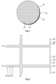
Figure 1 is a simplified top view of a wafer substrate with a plurality of semiconductor devices, each with a die portion surrounded by a peripheral portion. -
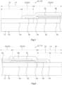
Figure 2 is a simplified top view of a detail of the wafer ofFigure 1 , showing dicing lanes surrounding semiconductor device dies. -
Figure 3 is a schematic top view of an embodiment of a semiconductor device as shown inFigures 1 and 2 , comprising drain, source and gate regions, each connected to a respective terminal. -
Figure 4 is a schematic view of another embodiment of a semiconductor device as shown inFigures 1 and 2 , comprising gate and drain regions, each connected to a respective terminal, and a source region connected to a plurality of terminals. -
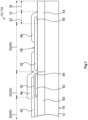
Figure 5 is a schematic cross-section of a detail of the drain region shown inFigure 3 or 4 . -
Figure 6 is a schematic cross-section of a detail of the source region shown inFigure 3 or 4 . -
Figure 7 is a schematic cross-section of a detail of the gate region shown inFigure 3 or 4 . -
Figure 8 is a schematic view of a further embodiment of a semiconductor device as shown inFigures 1 and 2 , comprising gate and drain regions, each connected to a respective terminal, and a source region connected to a plurality of terminals. -
Figure 9 is a schematic cross-section of a detail of the gate region shown inFigure 8 . - There will now be described by way of example specific modes contemplated by the inventors. In the following description and accompanying figures, numerous specific details are set forth in order to provide a thorough understanding, wherein like reference numerals designate like features. It will be readily apparent to one skilled in the art, that the present invention may be practiced without limitation to these specific details. In other instances, well known methods and structures have not been described in detail, to avoid obscuring the description unnecessarily.
- With reference to
Figures 1 and 2 , wherein like numerals correspond to like features, techniques described herein involve the manufacturing ofsemiconductor devices 10 on asubstrate 12, known in the art as a wafer, which is flat-sliced from an ingot of high-purity, single-crystalline silicon, typically cylindrical in shape. Eachwafer 12 is initially cleaned using various chemical processes to remove impurities and contaminants, then undergoes a series of processing steps to create thesemiconductor devices 10 thereon. - A semiconductor material is deposited onto the wafer's topside using known techniques, for example chemical vapor deposition (CVD) or physical vapor deposition (PVD). Then, in a photolithography process, a layer of light-sensitive photoresist is deposited onto the top surface of the wafer and exposed to ultraviolet light through an optical mask, for transferring a geometric pattern from the mask onto the photoresist. This pattern is typically a matrix of
semiconductor devices 10 delimited byinterstitial dicing lanes 14, also known in the art as saw lanes or scribe lines, depending upon the dicing technique employed. Conventionally, each dicing lane is a narrow strip of the underlying substrate material that surrounds the active area of the semiconductor device, created during the photolithography step of the manufacturing process as a border feature in the photomask, to define the boundaries of the device's active area, namely the region of the device wherein the electrical current flows. - According to the present technique, the mask is configured to avoid masking portions of dicing lanes, in such manner that each
semiconductor device 10 will comprise amain die portion 20, shown with a solid line inFigures 1 and 2 , surrounded by aperipheral portion 22, shown with a dotted line inFigure 2 , wherein the peripheral portion is located within a portion of the width of eachdicing lane 14 adjacent a respective side of amain die portion 20. Assemiconductor devices 10 of the example are substantially rectangular, accordingly each of themain die portion 20 and theperipheral portion 22 is rectangular, wherein adjacentperipheral portions 22 ofadjacent semiconductor devices 10 located in asame dicing lane 14 are separated by aninterstitial space 16 of semiconductor material that is lost to the dicing process. - The patterned
wafer 12 is then etched for removing excess semiconductor material, leaving behind the targeted pattern. Conventionally, this etching step removes semiconductor material in the dicing lanes. According to the present technique however, the etching step is configured to maintain semiconductor material in the form of a unitary member, described in further details hereafter, within theperipheral portion 22 of eachsemiconductor device 10 on the wafer. - The
etched wafer 12, including eachperipheral portion 22 in eachdicing lane 14 thereof, is then doped with impurities, such as boron or phosphorus, to create desired electrical properties. Thewafer 12 is annealed next, to activate the dopants and repair any damage caused by earlier steps. - Electrical contacts or terminals, described in further details hereafter, are then formed on the topside, or top surface, of the
wafer 12 to allow for electrical connections between the semiconductor devices and external circuits. At least some of these steps may repeated in order to create complex integrated circuits required by in modern electronic devices, until such time assemiconductor devices 10 can be individually cut from thewafer 10 along the dicinglanes 14. - With reference to
Figures 3 to 7 next, wherein like numerals correspond to like features, embodiments of a semiconductor device are shown both in top view inFigures 3 and 4 and in several cross-sectional views inFigures 5, 6 and7 . The structure of each semiconductor device follows the traditional MOSFET structure, in which the electric field is dropped vertically across an epitaxial drift layer, with bias applied at the drain on its underside, whilst the metal-oxide-semiconductor electron channel that is formed on and extends from the substrate topside, is substantially planar. - Each of the first embodiment of the
semiconductor device 10 and the second embodiment of thesemiconductor device 100 comprises agate region 30 formed on thedie portion 20 and electrically connected to agate terminal 32, asource region 40 formed in a first doped region of themain die portion 20 and electrically connected to at least onesource terminal 42 and surrounded by thegate region 30, and afirst drain region 50 formed in a second doped region of themain die portion 20 and electrically connected to adrain terminal 52. - In the first embodiment of the
semiconductor device 10, in a top view, thesource region 40 is located substantially centrally of themain die portion 20 intermediate to a main oblong portion of thegate region 30 and thefirst drain region 50, from which it is separated by an interstitial portion of thegate region 30. Thesource region 40 is electrically connected to onesource terminal 42, and thegate terminal 32, thesource terminal 42 and thedrain terminal 52 are arranged, in a top view perspective, as a line of three terminals equidistant one from the other. - In the second embodiment of the
semiconductor device 100, in a top view, thesource region 40 occupies approximately one half of themain die portion 20, with a main oblong portion of thesource region 40 located adjacent thegate region 30 and thefirst drain region 50 and an extension portion of thesource region 40 extending between a main oblong portion of thegate region 30 and thefirst drain region 50. Thesource region 40 is again surrounded by thegate region 30, including adjacent thefirst drain region 50, i.e. the main oblong portion and extension portion of thesource region 40 are separated from thefirst drain region 50 by an interstitial portion of thegate region 30. - In this second embodiment, the
source region 40 is electrically connected to twosource terminals gate terminal 32, thesource terminals drain terminal 52 are arranged, in a top view perspective, as a matrix of two columns of two terminals. A first column comprises thedrain terminal 52 and a source terminal 42a substantially aligned with each other and equidistant from one another. A second column comprises thegate terminal 32 and the second source terminal 42b substantially aligned with each other and equidistant one from the other. - The
gate terminal 32, the or eachsource terminal drain terminal 52 are made of an electrically conducting material, for example copper, aluminium or an alloy thereof, and located atop the surface of the semiconductor substrate. - Each embodiment of the
semiconductor device second drain region 54 formed in a doped region of theperipheral portion 22, comprising an elongateperipheral member 56 and electrically connected to thedrain terminal 52. The elongateperipheral member 56, shown with a short-dotted line inFigures 3 and 4 , is a runner member made of an electrically-conducting material, for instance the same material as thegate terminal 32, the or eachsource terminal drain terminal 52. Each of thesecond drain region 54 and the elongateperipheral member 56 accordingly surrounds themain die portion 20, inclusive of thegate region 30, thesource region 40 and thefirst drain region 50 formed thereon. - In a top view, the
second drain region 54 comprises first and second portions. The first portion of thesecond drain region 54 is contiguous with a majority portion of thegate region 30. In the first embodiment of thedevice 10, wherein the regions and their respective terminals are aligned, the first portion of thesecond drain region 54 corresponds to three sides of thegate region 30 distal thedrain region 50. In the second embodiment of thedevice 100, wherein the regions and their respective terminals are not aligned, thegate terminal 32 and thedrain terminal 52 are located at opposed corners of therectangular semiconductor device 100 on a same side of themain die portion 20, i.e. wherein thefirst drain region 50 occupies substantially 25% of the surface of themain die portion 20, as an oblong corner section thereof. The first portion of thesecond drain region 54 accordingly corresponds to two full sides and a portion of each of the remaining two sides of thegate region 30 distal thedrain region 50. - In a top view still, the second portion of the
second drain region 54, delimited with a long-dotted line inFigures 3 and 4 , is contiguous with a portion of thefirst drain region 50. In the first embodiment of thedevice 10, the second portion of thesecond drain region 54 corresponds to three sides of thefirst drain region 50 distal the gate andsource regions device 100, the second portion of thesecond drain region 54 corresponds to two orthogonal sides of thefirst drain region 50 distal the gate andsource regions second drain region 54 is effectively coplanar and integral with thefirst drain region 50, wherein each of thesecond drain region 54 and the elongateperipheral member 56 accordingly surrounds themain die portion 20 inclusive of thegate region 30,source region 40 andfirst drain region 50 formed thereon. - A detail of the
gate region 30 of bothembodiments Figure 5 , observing the device inFigure 3 from a left perspective and the device inFigure 4 from a top perspective, illustrating the first portion of thesecond drain region 54 contiguous with thegate region 30. - A detail of the gate and
source regions first embodiment Figure 6 , observing the device inFigure 3 from a bottom perspective, and illustrating the first portion of thesecond drain region 54 contiguous with the gate andsource regions - A detail of the
drain region 50 of bothembodiments Figure 7 , observing the device in eitherFigure 3 or Figure 4 from a right perspective, illustrating the second portion of thesecond drain region 54 contiguous and coplanar with thedrain region 50. - With reference to
Figures 5 to 7 , in the embodiments described herein, the substrate of thesemiconductor device 10 is used as the first andsecond drain regions substrate 12 forms anepitaxial layer 60 as the drift region, extending through thegate region 30 andsource region 40, underneath thegate terminal 32 and the or eachsource terminal 42. The doping of the second region of thesubstrate 12 forms a drain implant, extending through thedrain region 50 underneath thedrain terminal 52. - The doping of the
second drain region 54 of thesubstrate 12, with a same level of ion implantation as the first region and/or as the second region, or with a distinct level of ion implantation relative to both first and second regions, forms a peripheral drain implant in order to lead current out from aback surface 18 of thesubstrate 12 about the entire periphery of thesemiconductor device 10. In embodiments with asymmetric levels of ion implantation, a deeper level is preferred for thesecond drain region 54 relative to thefirst drain region 50. - In a cross-sectional perspective, the
epitaxial layer 60 extends from the top surface of thesubstrate 12 by a predetermined distance in a vertical direction, up to the lateral edge of themain die portion 20 in a horizontal direction, immediately adjacent the doped layer corresponding to thesecond drain regions 54 which extends from the top surface of thesubstrate 12 by the same predetermined distance, or a different predetermined distance, in a vertical direction. - In a cross-sectional perspective still, the or each
source terminal 42, thedrain terminal 52 and theperipheral member 56 are formed atop the substrate top surface opposite the substrate backsurface 18, whereas thegate terminal 32 is physically separated from thesubstrate 12 and thus the adjacent first andsecond drain regions epitaxial layer 60 of thesubstrate 12 to form an oxide layer, then depositing and growing to form polysilicon. Excess polysilicon and excess oxide layer, to be removed according to the semiconductor pattern, are etched through e.g. photolithography and etching. After etching, the oxide layer and polysilicon remaining on the surface of theepitaxial layer 60 respectively form agate oxide layer 62 and apolysilicon layer 64 intermediate theepitaxial layer 60 and thegate terminal 32. - A
passivation layer 66 is then applied to shield the top surface of the device from external contaminants, save for at least a respective portion of the top surface of each of thegate terminal 32 and the or eachsource terminal 42 and, as illustrated inFigure 7 , arespective portion 58 of the top surface of thedrain terminal 52, for electrical contact with an external circuit. - With reference to
Figures 8 and9 now, wherein like numerals correspond to like features, a further embodiment of asemiconductor device 110 is shown, the structure of which follows a CSP-packaged MOSFET structure. Thesemiconductor device 110 again comprises agate region 30 formed on thedie portion 20 and electrically connected to agate terminal 32, asource region 40 formed in a first doped region of themain die portion 20 and electrically connected to, in this example, foursource terminals first drain region 50 formed in a second doped region of themain die portion 20 and electrically connected to adrain terminal 52. - The
gate terminal 32, the foursource terminals 42a-42d and thedrain terminal 52 are for instance made of copper or aluminium and formed on the surface of thesemiconductor substrate 12 in an arrangement, in a top view perspective, of a matrix of two columns of three terminals. A first column comprises thegate terminal 32 and twosource terminals 42a-42b substantially aligned with each other and equidistant one from the other. A second column comprises thedrain terminal 52 and twosource terminals 42c-42d substantially aligned with each other and equidistant one from the other. - In top view still, terminals of respective columns are aligned with each other and the
gate terminal 32 and thedrain terminal 52 are located at opposed corners of therectangular semiconductor device 110, i.e. thegate terminal 32 is aligned with a source terminal 42c of the adjacent column distal to thedrain terminal 52 and thedrain terminal 52 is aligned with a source terminal 42a of the adjacent column distal to thegate terminal 32. Thesource region 40, located again substantially centrally of themain die portion 20, is asymmetrical according to the disposition of the foursource terminals 42a-42d, yet is again surrounded by thegate region 30, adjacent thefirst drain region 50 which occupies substantially 16% of the surface of themain die portion 20, as an oblong corner section thereof. - The
semiconductor device 110 further comprises thesecond drain region 54 formed in a doped region of theperipheral portion 22, comprising an elongateperipheral member 56 for instance made of copper or aluminium and electrically connected to thedrain terminal 52, shown with a short-dotted line inFigure 8 . In this example again, each of thesecond drain region 54 and the elongateperipheral member 56 accordingly surrounds themain die portion 20 inclusive of thegate region 30,source region 40 andfirst drain region 50 formed thereon. A first portion of thesecond drain region 54, delimited with a long-dotted line inFigure 5 , is contiguous with a portion of thefirst drain region 50, in this example corresponding to two orthogonal sides of thefirst drain region 50 distal the gate andsource regions second drain region 54 is contiguous with a portion of thegate region 30, in this example corresponding to four sides of thegate region 30 distal thedrain region 50. - In a cross-sectional perspective, the
gate terminal 32 is again physically separated from the first andsecond drain regions gate oxide layer 62 and apolysilicon layer 64 intermediate theepitaxial layer 60 and thegate terminal 32. The structure of thesemiconductor device 110 comprises further layers relative to the earlier example. - As a CSP packaged device, the
semiconductor device 110 comprises a packaging lid 80 intermediate themetallic terminals peripheral member 56, and lower layers of the structure, thus wherein the metallic terminals are intermediate the packaging lid 80 and thepassivation layer 66. - The
CSP device 110 of the third example also implements aspects of a trench MOSFET device, and accordingly includes trench arrangements to provide vertical active areas, implemented both in themain die portion 22 and in theperipheral portion 22. In the example shown inFigures 5 and 6 , an underside of eachmetallic terminal peripheral member 56 comprises one ormore projections 82, which are substantially V-shaped in cross-section and project downwards, towards thesubstrate 12. - At least one
projection 82 of ametallic terminal blind trench 84. Eachblind trench 84 is implemented by shaping the corresponding portion of the packaging lid 80 into a U-shape or similar, of a size complementing the terminal'sprojection 82. - One or more other projection(s) 82 of a
metallic terminal trench 86. Each through-trench 86 is implemented as a through hole in the corresponding portion of the packaging lid 80, of a shape and size complementing the metallic terminal'sprojection 82. - The or each
projection 82 of the metallicperipheral member 56 extends below the level of the member's underside abutting the topside of the packaging lid 80, into at least a portion of the depth of a corresponding through-trench 86 as described above. - A
further layer 90 of the structure of thesemiconductor device 110 is a portion of thepolysilicon layer 64 processed with an electrostatic discharge (`ESD') implantation method for improving the device's resilience to ESD events. TheESD layer 90 extends underneath thegate terminal 32 on a first side of the packaging lidblind trench 84, substantially coplanar with and adjacent thepolysilicon layer 64 located on the a second side of the packaging lidblind trench 84 opposite the first. Thegate oxide layer 62 extends underneath both theESD layer 90 and thepolysilicon layer 64 towards the lateral edge, but remains short of that edge to leave an interstitial space, through which an end portion of thepolysilicon layer 64 is in contact with theunderlying epitaxial layer 60. - Further to dicing a
semiconductor device gate terminal 32, an electric field is created in thegate oxide layer 62, which in turn creates an electric field in thesemiconductor material 60. This electric field controls the flow of current through theactive area semiconductor device 10. - Advantageously, the
second drain region 54 in theperipheral portion 22 and theperipheral drain member 56 can reduce between 20 and 30% of static device resistivity, relative to a conventional device structure consisting solely of adie portion 20, without requiring additional silicon and without reducing the active area of thedevice - In the specification the terms "comprise, comprises, comprised and comprising" or any variation thereof and the terms include, includes, included and including" or any variation thereof are considered to be totally interchangeable and they should all be afforded the widest possible interpretation and vice versa. The invention is not limited to the embodiments hereinbefore described but may be varied in both construction and detail.
Claims (15)
- A semiconductor device comprisinga semiconductor substrate comprising a die portion surrounded by a peripheral portion,a gate region formed on the die portion and connected to at least one gate terminal,a source region formed in a first doped region of the die portion and connected to at least one source terminal,a first drain region formed in a second doped region of the die portion and connected to at least one drain terminal, anda second drain region formed in a doped region of the peripheral portion, comprising a peripheral member electrically connected to the or each drain terminal,wherein the or each source terminal, gate terminal and drain terminal is formed on the surface of the semiconductor substrate andwherein the first and second drain regions lead out from a back surface of the substrate.
- The semiconductor device according to claim 1, wherein the peripheral portion is located in a dicing lane of a wafer comprising the semiconductor device.
- The semiconductor device according to claim 2, wherein a dimension of the peripheral portion corresponds to a portion of the dicing lane width.
- The semiconductor device according to any of claims 1 to 3, wherein a first portion of the second drain region is contiguous with a portion of the first drain region.
- The semiconductor device according to claim 4, wherein a second portion of the second drain region is contiguous with a portion of the gate region.
- The semiconductor device according to any of claims 1 to 5, wherein the peripheral portion is doped with a higher level of ion implantation relative to the die portion.
- The semiconductor device according to any of claims 1 to 6, wherein the second drain region is doped with a higher level of ion implantation relative to the first drain region.
- The semiconductor device according to any of claims 1 to 7, wherein the peripheral member is a metallic runner member.
- The semiconductor device according to any of claims 1 to 8, wherein the die portion and the peripheral portion are configured with one or more vertical active areas.
- The semiconductor device according to any of claims 1 to 9,wherein the first doped region is connected to four source terminals ; andwherein the gate region and the first drain region are formed on opposed corners of the die portion.
- A Chip Size Package ('CSP') device comprising at least one semiconductor device according to any of claims 1 to 10.
- A method of manufacturing a semiconductor device, comprising the steps of-depositing a semiconductor material on a wafer;generating a pattern of semiconductor devices and dicing lanes with a photolithography process, wherein a mask of the photolithography process is configured to avoid masking portions of dicing lanes, such that each semiconductor device in the pattern comprises a die portion surrounded by a peripheral portion located in the dicing lane portion;etching excess semiconductor material from the pattern, wherein the step of etching maintains semiconductor material in the form of a unitary member within each peripheral portion; anddoping each peripheral portion and at least a portion of each die portion.
- The method according to claim 12, wherein the step of doping further comprises doping each peripheral portion differently from each die portion.
- The method according to claim 13, wherein the step of doping further comprises doping each peripheral portion with a higher level of ion implantation relative to each die portion.
- The method according to any of claims 12 to 14, wherein the maintained unitary member is a metallic runner member.
Priority Applications (3)
| Application Number | Priority Date | Filing Date | Title |
|---|---|---|---|
| EP23175166.0A EP4468368A1 (en) | 2023-05-24 | 2023-05-24 | Semiconductor device with enhanced drain |
| CN202410644656.0A CN119029015A (en) | 2023-05-24 | 2024-05-23 | Semiconductor device with enhanced drain |
| US18/673,732 US20240395868A1 (en) | 2023-05-24 | 2024-05-24 | Semiconductor device with enhanced drain |
Applications Claiming Priority (1)
| Application Number | Priority Date | Filing Date | Title |
|---|---|---|---|
| EP23175166.0A EP4468368A1 (en) | 2023-05-24 | 2023-05-24 | Semiconductor device with enhanced drain |
Publications (1)
| Publication Number | Publication Date |
|---|---|
| EP4468368A1 true EP4468368A1 (en) | 2024-11-27 |
Family
ID=86603770
Family Applications (1)
| Application Number | Title | Priority Date | Filing Date |
|---|---|---|---|
| EP23175166.0A Pending EP4468368A1 (en) | 2023-05-24 | 2023-05-24 | Semiconductor device with enhanced drain |
Country Status (3)
| Country | Link |
|---|---|
| US (1) | US20240395868A1 (en) |
| EP (1) | EP4468368A1 (en) |
| CN (1) | CN119029015A (en) |
Citations (4)
| Publication number | Priority date | Publication date | Assignee | Title |
|---|---|---|---|---|
| US7855453B2 (en) * | 2007-03-30 | 2010-12-21 | Sanyo Electric Co., Ltd. | Semiconductor device |
| US8502314B2 (en) * | 2011-04-21 | 2013-08-06 | Fairchild Semiconductor Corporation | Multi-level options for power MOSFETS |
| US20140367770A1 (en) * | 2013-06-13 | 2014-12-18 | Renesas Electronics Corporation | Semiconductor device and method of manufacturing the same |
| US20180366576A1 (en) * | 2017-06-19 | 2018-12-20 | Ubiq Semiconductor Corp. | Semiconductor device and power conversion circuit |
-
2023
- 2023-05-24 EP EP23175166.0A patent/EP4468368A1/en active Pending
-
2024
- 2024-05-23 CN CN202410644656.0A patent/CN119029015A/en active Pending
- 2024-05-24 US US18/673,732 patent/US20240395868A1/en active Pending
Patent Citations (4)
| Publication number | Priority date | Publication date | Assignee | Title |
|---|---|---|---|---|
| US7855453B2 (en) * | 2007-03-30 | 2010-12-21 | Sanyo Electric Co., Ltd. | Semiconductor device |
| US8502314B2 (en) * | 2011-04-21 | 2013-08-06 | Fairchild Semiconductor Corporation | Multi-level options for power MOSFETS |
| US20140367770A1 (en) * | 2013-06-13 | 2014-12-18 | Renesas Electronics Corporation | Semiconductor device and method of manufacturing the same |
| US20180366576A1 (en) * | 2017-06-19 | 2018-12-20 | Ubiq Semiconductor Corp. | Semiconductor device and power conversion circuit |
Also Published As
| Publication number | Publication date |
|---|---|
| CN119029015A (en) | 2024-11-26 |
| US20240395868A1 (en) | 2024-11-28 |
Similar Documents
| Publication | Publication Date | Title |
|---|---|---|
| JP5111744B2 (en) | Metal oxide semiconductor device with enhanced shielding structure | |
| US6580134B1 (en) | Field effect transistors having elevated source/drain regions | |
| EP1610372B1 (en) | Fabrication method of a self aligned contact in a semiconductor device | |
| JPWO2013103051A1 (en) | Semiconductor device | |
| US11244830B2 (en) | Semiconductor device and manufacturing method thereof | |
| EP4589658A1 (en) | Power mosfet with gate-source esd diode structure | |
| US20200111713A1 (en) | Finfet having insulating layers between gate and source/drain contacts | |
| US12490445B2 (en) | Fabrication method of forming silicon carbide MOSFET | |
| US20240395868A1 (en) | Semiconductor device with enhanced drain | |
| WO2001069685A2 (en) | Trench-gate semiconductor devices | |
| EP3933895B1 (en) | Trench field effect transistor structure, and manufacturing method for same | |
| US10692992B2 (en) | Semiconductor device and fabrication method thereof | |
| CN103077941B (en) | Vertical electrostatic discharge protection element and manufacturing method thereof | |
| US20200020687A1 (en) | Using source/drain contact cap during gate cut | |
| CN112599601B (en) | Semiconductor device and method for manufacturing the same | |
| CN112490293B (en) | Semiconductor device and method of manufacturing the same | |
| US20250294802A1 (en) | Semiconductor device and method for forming the same | |
| US12166069B2 (en) | Semiconductor device and manufacturing method thereof | |
| TWI921913B (en) | Semiconductor device and method of manufacturing the same | |
| KR100345365B1 (en) | A method for fabricating a transistor of semiconductor device | |
| US12563772B2 (en) | Power MOSFET and manufacturing method thereof | |
| KR20110078978A (en) | Semiconductor device and manufacturing method thereof | |
| TW202606510A (en) | Semiconductor device and method of manufacturing the same | |
| CN118825067A (en) | Semiconductor device and method for manufacturing the same | |
| KR20030091533A (en) | MOS transistor having source/drain of triangle-type impurity doping profile and fabrication method thereof |
Legal Events
| Date | Code | Title | Description |
|---|---|---|---|
| PUAI | Public reference made under article 153(3) epc to a published international application that has entered the european phase |
Free format text: ORIGINAL CODE: 0009012 |
|
| STAA | Information on the status of an ep patent application or granted ep patent |
Free format text: STATUS: THE APPLICATION HAS BEEN PUBLISHED |
|
| AK | Designated contracting states |
Kind code of ref document: A1 Designated state(s): AL AT BE BG CH CY CZ DE DK EE ES FI FR GB GR HR HU IE IS IT LI LT LU LV MC ME MK MT NL NO PL PT RO RS SE SI SK SM TR |
|
| STAA | Information on the status of an ep patent application or granted ep patent |
Free format text: STATUS: REQUEST FOR EXAMINATION WAS MADE |
|
| 17P | Request for examination filed |
Effective date: 20250527 |