EP4468359A1 - Solid-state imaging element - Google Patents
Solid-state imaging element Download PDFInfo
- Publication number
- EP4468359A1 EP4468359A1 EP22928924.4A EP22928924A EP4468359A1 EP 4468359 A1 EP4468359 A1 EP 4468359A1 EP 22928924 A EP22928924 A EP 22928924A EP 4468359 A1 EP4468359 A1 EP 4468359A1
- Authority
- EP
- European Patent Office
- Prior art keywords
- transfer
- electrode
- region
- transfer electrode
- discharge gate
- Prior art date
- Legal status (The legal status is an assumption and is not a legal conclusion. Google has not performed a legal analysis and makes no representation as to the accuracy of the status listed.)
- Pending
Links
Images



Classifications
-
- H—ELECTRICITY
- H10—SEMICONDUCTOR DEVICES; ELECTRIC SOLID-STATE DEVICES NOT OTHERWISE PROVIDED FOR
- H10F—INORGANIC SEMICONDUCTOR DEVICES SENSITIVE TO INFRARED RADIATION, LIGHT, ELECTROMAGNETIC RADIATION OF SHORTER WAVELENGTH OR CORPUSCULAR RADIATION
- H10F39/00—Integrated devices, or assemblies of multiple devices, comprising at least one element covered by group H10F30/00, e.g. radiation detectors comprising photodiode arrays
- H10F39/10—Integrated devices
- H10F39/12—Image sensors
- H10F39/15—Charge-coupled device [CCD] image sensors
- H10F39/151—Geometry or disposition of pixel elements, address lines or gate electrodes
-
- H—ELECTRICITY
- H10—SEMICONDUCTOR DEVICES; ELECTRIC SOLID-STATE DEVICES NOT OTHERWISE PROVIDED FOR
- H10F—INORGANIC SEMICONDUCTOR DEVICES SENSITIVE TO INFRARED RADIATION, LIGHT, ELECTROMAGNETIC RADIATION OF SHORTER WAVELENGTH OR CORPUSCULAR RADIATION
- H10F39/00—Integrated devices, or assemblies of multiple devices, comprising at least one element covered by group H10F30/00, e.g. radiation detectors comprising photodiode arrays
- H10F39/80—Constructional details of image sensors
- H10F39/809—Constructional details of image sensors of hybrid image sensors
-
- H—ELECTRICITY
- H10—SEMICONDUCTOR DEVICES; ELECTRIC SOLID-STATE DEVICES NOT OTHERWISE PROVIDED FOR
- H10F—INORGANIC SEMICONDUCTOR DEVICES SENSITIVE TO INFRARED RADIATION, LIGHT, ELECTROMAGNETIC RADIATION OF SHORTER WAVELENGTH OR CORPUSCULAR RADIATION
- H10F39/00—Integrated devices, or assemblies of multiple devices, comprising at least one element covered by group H10F30/00, e.g. radiation detectors comprising photodiode arrays
- H10F39/10—Integrated devices
- H10F39/12—Image sensors
- H10F39/15—Charge-coupled device [CCD] image sensors
- H10F39/153—Two-dimensional or three-dimensional array CCD image sensors
- H10F39/1536—Frame transfer
-
- H—ELECTRICITY
- H04—ELECTRIC COMMUNICATION TECHNIQUE
- H04N—PICTORIAL COMMUNICATION, e.g. TELEVISION
- H04N25/00—Circuitry of solid-state image sensors [SSIS]; Control thereof
- H04N25/70—SSIS architectures; Circuits associated therewith
- H04N25/71—Charge-coupled device [CCD] sensors; Charge-transfer registers specially adapted for CCD sensors
-
- H—ELECTRICITY
- H04—ELECTRIC COMMUNICATION TECHNIQUE
- H04N—PICTORIAL COMMUNICATION, e.g. TELEVISION
- H04N25/00—Circuitry of solid-state image sensors [SSIS]; Control thereof
- H04N25/70—SSIS architectures; Circuits associated therewith
- H04N25/76—Addressed sensors, e.g. MOS or CMOS sensors
- H04N25/77—Pixel circuitry, e.g. memories, A/D converters, pixel amplifiers, shared circuits or shared components
- H04N25/772—Pixel circuitry, e.g. memories, A/D converters, pixel amplifiers, shared circuits or shared components comprising A/D, V/T, V/F, I/T or I/F converters
-
- H—ELECTRICITY
- H04—ELECTRIC COMMUNICATION TECHNIQUE
- H04N—PICTORIAL COMMUNICATION, e.g. TELEVISION
- H04N25/00—Circuitry of solid-state image sensors [SSIS]; Control thereof
- H04N25/70—SSIS architectures; Circuits associated therewith
- H04N25/76—Addressed sensors, e.g. MOS or CMOS sensors
- H04N25/77—Pixel circuitry, e.g. memories, A/D converters, pixel amplifiers, shared circuits or shared components
- H04N25/778—Pixel circuitry, e.g. memories, A/D converters, pixel amplifiers, shared circuits or shared components comprising amplifiers shared between a plurality of pixels, i.e. at least one part of the amplifier must be on the sensor array itself
-
- H—ELECTRICITY
- H10—SEMICONDUCTOR DEVICES; ELECTRIC SOLID-STATE DEVICES NOT OTHERWISE PROVIDED FOR
- H10F—INORGANIC SEMICONDUCTOR DEVICES SENSITIVE TO INFRARED RADIATION, LIGHT, ELECTROMAGNETIC RADIATION OF SHORTER WAVELENGTH OR CORPUSCULAR RADIATION
- H10F39/00—Integrated devices, or assemblies of multiple devices, comprising at least one element covered by group H10F30/00, e.g. radiation detectors comprising photodiode arrays
- H10F39/10—Integrated devices
- H10F39/12—Image sensors
- H10F39/15—Charge-coupled device [CCD] image sensors
- H10F39/158—Charge-coupled device [CCD] image sensors having arrangements for blooming suppression
Definitions
- the present disclosure relates to a solid-state imaging element.
- Non Patent Literatures 1 and 2 describe a monolithic CCD-CMOS as a solid-state imaging element of the related art.
- the monolithic CCD-CMOS is a solid-state imaging element in which a CCD unit that generates charges in response to incidence of light and transfers the charges and a CMOS unit that processes a digital signal corresponding to the charges are formed on a single semiconductor substrate.
- a plurality of transfer electrodes and discharge gate electrodes are disposed in the same layer, and gaps are formed between adjacent transfer electrodes and between each transfer electrode and the discharge gate electrode.
- the charges may be trapped in a region corresponding to each gap in the semiconductor substrate, and the transfer of the charges and the discharge of the charges may not be appropriately performed.
- An object of the present disclosure is to provide a solid-state imaging element capable of securing appropriate characteristics.
- a solid-state imaging element includes a semiconductor substrate, a first element unit formed on the semiconductor substrate, and a second element unit formed on the semiconductor substrate, the first element unit includes a light receiving part configured to generate charges in response to incidence of light, and a transfer part configured to transfer charges, the second element unit is configured to perform at least one of transmission of a signal to the first element unit and reception of a signal from the first element unit, the transfer part includes a first transfer electrode and a second transfer electrode that are disposed over a charge transfer region of the semiconductor substrate, and are aligned in a transfer direction of the charges, and a discharge gate electrode that is disposed over a charge discharge region of the semiconductor substrate along the charge transfer region, the first transfer electrode is formed as a first layer, the second transfer electrode and the discharge gate electrode are formed as second layers different from the first layer, as viewed from a thickness direction of the semiconductor substrate, the first transfer electrode includes a portion overlapping a part of the second transfer electrode and a portion overlapping a part of the discharge gate electrode
- the first transfer electrode includes the portion overlapping the part of the second transfer electrode and the portion overlapping the part of the discharge gate electrode. As a result, it is less likely to form the gaps between the first transfer electrode and the second transfer electrode and between the first transfer electrode and the discharge gate electrode as viewed from the thickness direction of the semiconductor substrate. Thus, in the charge transfer region and the charge discharge region, it is possible to suppress generation of a region where charges are trapped, and it is possible to appropriately perform the transfer of the charges and the discharge of the charges.
- the layer structure of the electrodes included in the first element unit is three or more layers, it is difficult to form the electrodes and the like included in the second element unit with high accuracy.
- the layer structure of the first transfer electrode, the second transfer electrode, and the discharge gate electrode included in the first element unit has two layers, the electrode and the like included in the second element unit can be formed with high accuracy. As described above, according to the solid-state imaging element, appropriate characteristics can be secured.
- the part of the second transfer electrode and the part of the discharge gate electrode may be positioned on the same side with respect to the first transfer electrode in the thickness direction of the semiconductor substrate. According to this configuration, the layer structure of the first transfer electrode, the second transfer electrode, and the discharge gate electrode included in the first element unit can be formed into two layers with a simple structure.
- the transfer part may further include an insulating layer extending as the same layer between the first transfer electrode and the part of the second transfer electrode and between the first transfer electrode and the part of the discharge gate electrode.
- the charge discharge region may include a drain region, and the discharge gate electrode and the drain region extend in the transfer direction. According to this configuration, surplus charges in the charge transfer region can be appropriately discharged to the drain region, and an anti-blooming property of the solid-state imaging element can be improved.
- the first element unit may include an amplifier part configured to convert the charge transferred by the transfer part into an analog signal
- the second element unit includes a conversion part configured to convert the analog signal into a digital signal. According to this configuration, the solid-state imaging element can convert the analog signal into the digital signal that is hardly influenced by noise.
- the charge transfer region may include a first transfer region and a second transfer region having an impurity concentration different from an impurity concentration of the first transfer region, the first transfer electrode may be disposed over the first transfer region, and the second transfer electrode may be disposed over the second transfer region.
- a two-phase driving method can be used as a charge transfer method in the transfer part, and an operation of the first element unit can be realized with a control voltage of a minimum number of phases (two phases).
- the solid-state imaging element capable of securing appropriate characteristics.
- a solid-state imaging element 1 includes a semiconductor substrate 2, a first element unit 3, and a second element unit 4.
- the first element unit 3 and the second element unit 4 are formed on a single semiconductor substrate 2.
- the second element unit 4 is configured to receive a signal from the first element unit 3.
- the first element unit 3 is, for example, a charge coupled device (CCD) unit
- the second element unit 4 is, for example, a complementary metal oxide semiconductor (CMOS) unit. That is, the solid-state imaging element 1 is, for example, a monolithic CCD-CMOS.
- CCD charge coupled device
- CMOS complementary metal oxide semiconductor
- a thickness direction of the semiconductor substrate 2 is referred to as a Z direction
- one direction perpendicular to the Z direction is referred to as an X direction
- a direction perpendicular to both directions of the Z direction and the X direction is referred to as a Y direction.
- the semiconductor substrate 2 has, for example, a rectangular shape as viewed from the Z direction. A longitudinal direction of the semiconductor substrate 2 is along the X direction.
- the semiconductor substrate 2 includes a base portion 10 and a semiconductor layer 20.
- the base portion 10 has a P-type conductivity type.
- the base portion 10 is, for example, a silicon substrate.
- the base portion 10 has a surface 10a and a surface 10b perpendicular to the Z direction.
- the surface 10b has an opened recessed portion 11.
- the recessed portion 11 has, for example, a quadrangular frustum shape expanding from the surface 10a toward the surface 10b.
- the recessed portion 11 penetrates the base portion 10. Accordingly, the semiconductor layer 20 is exposed at a bottom portion of the recessed portion 11.
- the recessed portion 11 is formed by, for example, etching.
- a thickness of the portion of the base portion 10 where the recessed portion 11 is not formed is, for example, about 300 ⁇ m.
- the semiconductor layer 20 is formed on the surface 10a of the base portion 10.
- the semiconductor layer 20 is, for example, an epitaxial growth layer containing silicon.
- a thickness of the semiconductor layer 20 is, for example, about 10 ⁇ m.
- the first element unit 3 and the second element unit 4 are formed in the semiconductor layer 20.
- the first element unit 3 includes a light receiving part 31, a transfer part 32, and an amplifier part 33.
- the light receiving part 31 generates charges in response to incidence of light hv.
- the light receiving part 31 is formed at a position overlapping the recessed portion 11 in the Z direction.
- the light hv is incident on the light receiving part 31 from the surface 10b side of the base portion 10 via the recessed portion 11.
- the light receiving part 31 includes, for example, a plurality of pixels aligned two-dimensionally along the X direction and the Y direction.
- the transfer part 32 transfers the charges generated in the light receiving part 31.
- the transfer part 32 transfers the charges along the X direction for each pixel array extending along the X direction.
- the amplifier part 33 converts the charge transferred by the transfer part 32 into an analog signal (signal voltage).
- the amplifier part 33 is electrically connected to the transfer part 32 by a wiring W1.
- the analog signal converted by the amplifier part 33 is transmitted to the second element unit 4.
- the second element unit 4 includes a signal processing part 40.
- the signal processing part 40 processes a digital signal corresponding to the charge transferred by the transfer part 32.
- the signal processing part 40 includes a conversion part 41, a drive part 42, a multiplexer part 43, and an output part 44.
- the conversion part 41 converts the analog signal received from the first element unit 3 into a digital signal.
- the conversion part 41 is electrically connected to the amplifier part 33 by a wiring W2.
- the drive part 42 generates a signal for driving the conversion part 41.
- the drive part 42 includes, for example, a phase locked loop (PLL) and a timing generator.
- PLL phase locked loop
- the drive part 42 is electrically connected to the conversion part 41 by a wiring W3.
- the multiplexer part 43 bundles a plurality of digital signals converted by the conversion part 41 to generate one digital signal.
- the multiplexer part 43 is electrically connected to the conversion part 41 by a wiring W4.
- the output part 44 converts the digital signal from the multiplexer part 43 into a differential voltage signal and outputs the differential voltage signal to an outside.
- the output part 44 includes, for example, a low voltage differential signaling (LVDS) part.
- the output part 44 is electrically connected to the multiplexer part 43 by a wiring W5.
- the semiconductor layer 20 includes a semiconductor region 21, a semiconductor region 22, and a plurality of semiconductor regions 23.
- the semiconductor region 21 has a P-type conductivity type, and is formed on the surface 10a of the base portion 10.
- the semiconductor region 22 has an N-type conductivity type, and is formed on the semiconductor region 21.
- Each semiconductor region 23 has an N - -type conductivity type.
- the "N - -type” means that a concentration of an N-type impurity is lower than that of the "N-type”.
- Each semiconductor region 23 is formed within the semiconductor region 22 along a surface of the semiconductor region 22 opposite to the semiconductor region 21.
- the light receiving part 31 includes a PN junction region formed in the semiconductor layer 20. Specifically, the PN junction region is formed at a boundary portion between the semiconductor region 21 and the semiconductor region 22. When the light hv is incident on the PN junction region formed in the semiconductor layer 20, the charges are generated.
- the transfer part 32 includes a charge transfer region 70, a charge discharge region 75, a plurality of transfer electrodes 80, a discharge gate electrode 85, and a plurality of insulating layers 90.
- the charge transfer region 70 is formed within the semiconductor layer 20.
- the charge transfer region 70 includes the semiconductor region 22 and the semiconductor region 23, and transfers the charge generated in the light receiving part 31.
- the charge transfer region 70 includes a plurality of first transfer regions 71 and a plurality of second transfer regions 72.
- the first transfer region 71 of the present embodiment is a region positioned between two semiconductor regions 22 aligned in the X direction in the semiconductor region 23, and overlaps a first transfer electrode 81 to be described later in the Z direction.
- the first transfer region 71 does not include the semiconductor region 23.
- the second transfer region 72 of the present embodiment is a region including the semiconductor region 23, and overlaps a second transfer electrode 82 to be described later in the Z direction.
- the first transfer region 71 and the second transfer region 72 are alternately aligned in a transfer direction of the charges (X direction).
- the semiconductor region 22 has an N-type conductivity type
- the semiconductor region 23 has an N - -type conductivity type. Accordingly, an impurity concentration of the first transfer region 71 not including the semiconductor region 23 is different from an impurity concentration of the second transfer region 72 including the semiconductor region 23. Specifically, the impurity concentration of the first transfer region 71 is higher than the impurity concentration of the second transfer region 72.
- the plurality of transfer electrodes 80 are disposed over the charge transfer region 70 and includes a plurality of first transfer electrodes 81 and a plurality of second transfer electrodes 82.
- the first transfer electrode 81 and the second transfer electrode 82 are made of, for example, polysilicon.
- the first transfer electrode 81 and the second transfer electrode 82 are electrodes that transfer the charges generated in the light receiving part 31 in the X direction.
- the first transfer electrode 81 and the second transfer electrode 82 transfer the charges for each pixel array extending along the X direction.
- the first transfer electrode 81 is disposed over the first transfer region 71, and the second transfer electrode 82 is disposed over the second transfer region 72.
- the first transfer electrode 81 and the second transfer electrode 82 are alternately aligned in the transfer direction of the charges (X direction).
- the first transfer electrode 81 has, for example, a rectangular shape as viewed from the Z direction.
- a longitudinal direction of the first transfer electrode 81 is along the Y direction.
- a shape of the first transfer electrode 81 as viewed from the Z direction is not limited.
- the first transfer electrode 81 has a flat plate shape along the X direction and the Y direction.
- the first transfer electrode 81 has a pair of surfaces 81a and 81b opposed to each other in the Z direction.
- the surfaces 81a and 81b are along the X direction and the Y direction.
- the surface 81a is positioned farther from the semiconductor substrate 2 than the surface 81b.
- the first transfer electrode 81 has a pair of overlapping portions A1 overlapping a part (overlapping portion A2) of the second transfer electrode 82.
- the pair of overlapping portions A1 is positioned at both end portions of the first transfer electrode 81 in the X direction.
- the second transfer electrode 82 has, for example, a rectangular shape as viewed from the Z direction.
- a longitudinal direction of the second transfer electrode 82 is along the Y direction.
- a shape of the second transfer electrode 82 as viewed from the Z direction is not limited.
- the second transfer electrode 82 includes a first portion 83 and a pair of second portions 84.
- the first portion 83 has a flat shape along the X direction and the Y direction.
- the first portion 83 is spaced apart from the semiconductor layer 20 by the same distance as a distance from the semiconductor layer 20 to the first transfer electrode 81.
- the first portion 83 has a pair of surfaces 83a and 83b opposed to each other in the Z direction.
- the surface 83b is positioned closer to the semiconductor layer 20 than the surface 83a, and is at the same height as the surface 81b of the first transfer electrode 81.
- the second portion 84 is positioned farther from the semiconductor layer 20 than the first portion 83 in the Z direction.
- the second portion 84 is formed to be bent from the Z direction to the X direction in XZ sectional view.
- the second portion 84 has a portion along the Y direction and the Z direction and a portion along the X direction and the Y direction.
- the portion of the second portion 84 along the Y direction and the Z direction is continuous with corresponding an end portion of both end portions of the first portion 83 in the X direction.
- the second portion 84 has an overlapping portion A2.
- the overlapping portion A2 is a portion overlapping the overlapping portion A1 of the first transfer electrode 81 as viewed from the Z direction.
- the overlapping portion A2 is positioned on the surface 81a side with respect to the first transfer electrode 81 in the Z direction. As viewed from the Z direction, a gap is not formed between the first transfer electrode 81 and the second transfer electrode 82.
- the charge discharge region 75 is a region where the charges are discharged from the charge transfer region 70.
- the charge discharge region 75 is along the charge transfer region 70 and is adjacent to the charge transfer region 70 in the Y direction.
- the charge discharge region 75 includes a drain region 76.
- the drain region 76 is a region from which surplus charges within the charge transfer region 70 are discharged.
- the drain region 76 extends in the X direction.
- the drain region 76 has an N + -type conductivity type.
- the "N + -type" means that a concentration of an N-type impurity is higher than that of the "N-type".
- the discharge gate electrode 85 is disposed over the charge discharge region 75.
- the discharge gate electrode 85 extends in the X direction. That is, the discharge gate electrode 85 and the drain region 76 extend in the same direction.
- the discharge gate electrode 85 has, for example, a rectangular shape as viewed from the Z direction.
- a longitudinal direction of the discharge gate electrode 85 is along the X direction.
- a shape of the discharge gate electrode 85 as viewed from the Z direction is not limited.
- the discharge gate electrode 85 includes a first portion 86 and a second portion 87.
- the first portion 86 has a flat shape along the X direction and the Y direction.
- the first portion 86 is spaced apart from the semiconductor layer 20 by the same distance as the distance from the semiconductor layer 20 to the first transfer electrode 81.
- the surface 86b closer to the semiconductor layer 20 is at the same height as the surface 81b of the first transfer electrode 81.
- the first portion 86 overlaps the drain region 76 in the Z direction.
- the second portion 87 is positioned farther from the semiconductor layer 20 than the first portion 86 in the Z direction.
- the second portion 87 is formed to be bent from the Z direction to the Y direction in YZ sectional view.
- the second portion 87 has a portion along the X direction and the Z direction and a portion along the X direction and the Y direction.
- the portion of the second portion 87 along the X direction and the Z direction is continuous with an end portion on the charge transfer region 70 side of both end portions of the first portion 86 in the Y direction.
- the first transfer electrode 81 has an overlapping portion A3 overlapping a part (overlapping portion A4) of the discharge gate electrode 85.
- the overlapping portion A3 is positioned at an end portion on the charge discharge region 75 side of both end portions of the first transfer electrode 81 in the Y direction.
- the second portion 87 of the discharge gate electrode 85 has an overlapping portion A4.
- the overlapping portion A4 is a portion overlapping the overlapping portion A3 of the first transfer electrode 81 as viewed from the Z direction.
- the overlapping portion A4 is positioned on the surface 81a side with respect to the first transfer electrode 81 in the Z direction.
- the overlapping portion A2 of the second transfer region 72 and the overlapping portion A4 of the discharge gate electrode 85 are positioned on the same side with respect to the first transfer electrode 81 in the Z direction. As viewed from the Z direction, a gap is not formed between the first transfer electrode 81 and the discharge gate electrode 85.
- the discharge gate electrode 85 extends over the plurality of first transfer electrodes 81 aligned spaced apart in the X direction. That is, the common discharge gate electrode 85 extends to overlap the plurality of first transfer electrodes 81.
- the second transfer electrode 82 is spaced apart from the discharge gate electrode 85. That is, as viewed from the Z direction, a gap is formed between the second transfer electrode 82 and the discharge gate electrode 85. In the present embodiment, the second transfer electrode 82 is spaced apart from the discharge gate electrode 85 in the Y direction. As viewed from the Z direction, a width of the gap between the discharge gate electrode 85 and the second transfer electrode 82 in the Y direction is smaller than an interval between the first transfer electrodes 81 adjacent in the X direction. The second transfer electrode 82 is not in contact with the discharge gate electrode 85 and does not overlap the discharge gate electrode 85 in the Z direction.
- a layer structure of the electrodes (first transfer electrode 81, second transfer electrode 82, and discharge gate electrode 85) included in the solid-state imaging element 1 has a two-layer structure.
- the first transfer electrode 81 is formed as a first layer
- the second transfer electrode 82 and the discharge gate electrode 85 are formed as second layers different from the first layer.
- the "first layer” and the "second layer” correspond to timings at which layers are formed in ae manufacturing process of the solid-state imaging element 1.
- the layer formed as the first layer is a layer that cannot be formed simultaneously with the layer formed as the second layer.
- the first transfer electrode 81 since a part of the first transfer electrode 81 overlaps the second transfer electrode 82 and the discharge gate electrode 85, the first transfer electrode 81 cannot be formed simultaneously with the second transfer electrode 82 and the discharge gate electrode 85.
- the first transfer electrode 81 is formed before the formation of the second transfer electrode 82 and the discharge gate electrode 85.
- layers formed as the same layer can be simultaneously formed.
- the second transfer electrode 82 and the discharge gate electrode 85 formed as the same second layer are simultaneously formed after the first transfer electrode 81 is formed.
- the layers formed as the same layer may be layers that can be simultaneously formed, and may not necessarily be simultaneously formed.
- the second transfer electrode 82 and the discharge gate electrode 85 may be formed at different timings.
- the plurality of insulating layers 90 are formed on the semiconductor layer 20.
- Each insulating layer 90 is a layer made of, for example, silicon oxide.
- the silicon oxide is, for example, SiO 2 .
- a thickness of each insulating layer 90 is, for example, about several tens to several hundreds nm.
- the plurality of insulating layers 90 electrically separate the first transfer electrode 81, the second transfer electrode 82, and the discharge gate electrode 85 from each other. In FIGS. 3 and 4 , only an insulating layer 91 among the plurality of insulating layers 90 is indicated by a dashed double-dotted line for the sake of convenience in description.
- the insulating layer 91 extends, as the same layer, between the overlapping portion A1 of the first transfer electrode 81 and the overlapping portion A2 of the second transfer electrode 82 and between the overlapping portion A3 of the first transfer electrode 81 and the overlapping portion A4 of the discharge gate electrode 85.
- the insulating layer 91 is continuously formed along the surface 81a of the first transfer electrode 81 to extend from between the overlapping portion A1 and the overlapping portion A2 to between the overlapping portion A3 and the overlapping portion A4.
- the second element unit 4 includes a first electrode 101, a second electrode 102, and a plurality of third electrodes 103 formed on the semiconductor layer 20.
- the first electrode 101, the second electrode 102, and the plurality of third electrodes 103 are included in the signal processing part 40 (see FIG. 1 ) of the second element unit 4, and are included, for example, in any of the conversion part 41, the drive part 42, the multiplexer part 43, and the output part 44.
- the first electrode 101, the second electrode 102, and the plurality of third electrodes 103 are made of, for example, polysilicon.
- the first electrode 101 and the second electrode 102 overlap each other in the Z direction, and constitute, for example, a capacitor.
- the plurality of third electrodes 103 are aligned in the X direction, and constitute, for example, a gate electrode of a field effect transistor (FET).
- FET field effect transistor
- the first electrode 101 is formed as the first layer. That is, the first electrode 101 can be formed simultaneously with the first transfer electrode 81 of the first element unit 3. The first electrode 101 is spaced apart from the semiconductor layer 20 by the same distance as the distance from the semiconductor layer 20 to the first transfer electrode 81.
- the second electrode 102 is formed as a second layer. That is, the second electrode 102 can be formed simultaneously with the second transfer electrode 82 of the first element unit 3. The second electrode 102 is spaced apart from the semiconductor layer 20 by the same distance as the distance from the semiconductor layer 20 to the second portion 84 of the second transfer electrode 82.
- the first electrode 101 and the second electrode 102 of the second element unit 4 have a two-layer structure.
- the third electrode 103 is spaced apart from the semiconductor layer 20 by the same distance as the distance from the semiconductor layer 20 to the first transfer electrode 81.
- the third electrode 103 may be formed simultaneously with the first electrode 101 or the second electrode 102.
- the second element unit 4 has a plurality of insulating layers 95 formed on the semiconductor layer 20.
- the insulating layer 95 is formed integrally with the insulating layer 90 of the first element unit 3.
- Each insulating layer 95 is a layer made of, for example, silicon oxide.
- the silicon oxide is, for example, SiO 2 .
- the plurality of insulating layers 95 electrically separate the first electrode 101, the second electrode 102, and the third electrode 103 from each other.
- only an insulating layer 96 among the plurality of insulating layers 90 is indicated by a dashed double-dotted line for the sake of convenience in description.
- the insulating layer 96 is formed from between the first electrode 101 and the second electrode 102 to the third electrode 103.
- the insulating layer 96 is continuous with the insulating layer 91 included in the first element unit 3, and can be formed simultaneously with the insulating layer 91. That is, the insulating layer positioned between the electrode formed as the first layer and the electrode formed as the second layer in the second element unit 4 can be formed simultaneously with the insulating layer positioned between the electrode formed as the first layer and the electrode formed as the second layer in the first element unit 3.
- a thickness of a portion 96a of the insulating layer 96 positioned between the first electrode 101 and the second electrode 102 is equal to a thickness of a portion 91a of the insulating layer 91 positioned between the overlapping portion A1 of the first transfer electrode 81 and the overlapping portion A2 of the second transfer electrode 82.
- the solid-state imaging element 1 when the light hv is incident on the light receiving part 31, the charges are generated in each pixel of the light receiving part 31.
- the charges are transferred to the amplifier part 33 by the transfer part 32.
- the charges are transferred along the X direction from a left side to a right side in FIG. 3 .
- the transfer method of the charges will be described with reference to FIG. 3 .
- a two-phase driving method is used as the charge transfer method.
- first transfer regions 71A and 71B are referred to as first transfer regions 71A and 71B
- second transfer regions 72 are referred to as second transfer regions 72A and 72B.
- first transfer electrode 81 over the first transfer region 71A is referred to as a first transfer electrode 81A
- first transfer electrode 81 over the first transfer region 71B is referred to as a first transfer electrode 81B
- second transfer electrode 82 over the second transfer region 72A is referred to as a second transfer electrode 82A
- the second transfer electrode 82 over the second transfer region 72B is referred to as a second transfer electrode 82B.
- the first transfer region 71A has an impurity concentration higher than that of the second transfer region 72A.
- a potential well formed under the first transfer electrode 81A is deeper than a potential well formed under the second transfer electrode 82A. Due to this potential difference, the charges generated in the light receiving part 31 flow from the second transfer region 72A into the first transfer region 71A and are stored in the first transfer region 71A. That is, the first transfer region 71A functions as a storage that stores the charges.
- the other first transfer regions 71 similarly function as storages.
- the potential well under the second transfer electrode 82A is shallower than the potential well under the first transfer electrode 81A, the charges do not flow back from the first transfer region 71A to the second transfer region 72A. That is, the second transfer region 72A functions as a barrier that prevents a backflow of the charges.
- the other second transfer regions 72 similarly function as barriers.
- a depth of the potential well gradually becomes deeper from the first transfer region 71A toward the first transfer region 71B.
- the charges stored in the first transfer region 71A pass through the second transfer region 72B and are transferred to the first transfer region 71B.
- the charges are transferred in the X direction by repeating the above transfer method also in the other first transfer electrodes 81 and second transfer electrodes 82.
- the charges may be discharged from the charge transfer region 70 to the charge discharge region 75.
- the charges may be discharged from the charge transfer region 70 to the charge discharge region 75.
- a part of the charges is discharged to the drain region 76 of the charge discharge region 75.
- a discharge method of the charges will be described with reference to FIG. 4 .
- a value of a voltage P3 applied to the discharge gate electrode 85 is increased to an appropriate value.
- a potential well under the discharge gate electrode 85 becomes deep (the potential barrier becomes low), and the charges are discharged from the charge transfer region 70 to the charge discharge region 75.
- the drain region 76 has an N + -type conductivity type and has a high impurity concentration.
- the charge discharged to the charge discharge region 75 mainly flow into the drain region 76.
- the charges transferred in the X direction by the first transfer electrode 81 and the second transfer electrode 82 are sent to the amplifier part 33.
- the charges are sent to the amplifier part 33 for each pixel array extending along the X direction.
- the electric charge is converted into an analog signal in the amplifier part 33.
- the analog signal converted by the amplifier part 33 is converted into a digital signal by the conversion part 41.
- the plurality of digital signals converted by the conversion part 41 are bundled in the multiplexer part 43 and are generated as one digital signal. This digital signal is converted into a differential voltage signal in the output part 44 and is output to the outside.
- the first transfer electrode 81 includes the overlapping portion A1 overlapping the overlapping portion A2 of the second transfer electrode 82 and the overlapping portion A3 overlapping the overlapping portion A4 of the discharge gate electrode 85.
- the charge transfer region 70 and the charge discharge region 75 it is possible to suppress generation of a region where charges are trapped, and it is possible to appropriately perform the transfer of the charges and the discharge of the charges.
- the layer structure of the electrodes included in the first element unit 3 is three or more layers
- a step is generated between the first element unit 3 and the second element unit 4, and a resolution when the electrode or the like of the second element unit 4 is formed by photolithography is reduced.
- the layer structure of the first transfer electrode 81, the second transfer electrode 82, and the discharge gate electrode 85 included in the first element unit 3 is two layers.
- the step is hardly generated between the first element unit 3 and the second element unit 4, and it is possible to form an electrode or the like included in the second element unit 4 with high accuracy.
- appropriate characteristics can be secured.
- the first transfer electrode 81 disposed over the first transfer region 71 functioning as the storage overlaps the discharge gate electrode 85
- the second transfer electrode 82 disposed over the second transfer region 72 functioning as the barrier does not overlap the discharge gate electrode 85.
- the charges are efficiently discharged from the first transfer region 71 in which more charges are stored than in the second transfer region 72 to the charge discharge region 75, and it is possible to avoid the layer structure of the electrodes (first transfer electrode 81, second transfer electrode 82, and discharge gate electrode 85) included in the first element unit 3 from having a three-layer structure.
- the overlapping portion A1 of the first transfer electrode 81 and the overlapping portion A2 of the second transfer electrode 82 overlap each other, and thus, the generation of the region where the charges are trapped is suppressed.
- the solid-state imaging element 1 it is not necessary to excessively narrow an interval between the first transfer electrode 81 and the discharge gate electrode 85 in the XY plane (specifically, an interval between the first transfer electrode 81 and the first portion 86 of the discharge gate electrode 85) in order to suppress the generation of the region where the charge is trapped.
- an interval between the first transfer electrode 81 and the discharge gate electrode 85 in the XY plane specifically, an interval between the first transfer electrode 81 and the first portion 86 of the discharge gate electrode 85
- the first transfer electrode is formed as the second layer to overlap a part of the discharge gate electrode, and the second transfer electrode is formed as the third layer to overlap a part of the discharge gate electrode and a part of the first transfer electrode, the first transfer electrode does not have a flat shape.
- the first transfer electrode rides over the discharge gate electrode, and has a hollow due to a thickness of the discharge gate electrode.
- a material of the second transfer electrode that has entered the hollow of the first transfer electrode may remain as a residue without being removed by etching.
- the first transfer electrode 81 has a flat shape.
- the material of the second transfer electrode 82 hardly remains as the residue on the first transfer electrode 81, and the short circuit between the second transfer electrodes 82 can be suppressed. Accordingly, according to the solid-state imaging element 1, appropriate characteristics can be secured.
- the overlapping portion A2 of the second transfer electrode 82 and the overlapping portion A4 of the discharge gate electrode 85 are positioned on the same side with respect to the first transfer electrode 81 in the thickness direction of the semiconductor substrate 2. According to this configuration, the layer structure of the first transfer electrode 81, the second transfer electrode 82, and the discharge gate electrode 85 included in the first element unit 3 can be formed into two layers with a simple structure.
- the transfer part 32 further includes the insulating layer 91 extending as the same layer between the first transfer electrode 81 and the overlapping portion A2 of the second transfer electrode 82 and between the first transfer electrode 81 and the overlapping portion A4 of the discharge gate electrode 85.
- the layer structure of the first transfer electrode 81, the second transfer electrode 82, and the discharge gate electrode 85 included in the first element unit 3 can be formed into two layers with a simple structure.
- the charge discharge region 75 includes the drain region 76, and the discharge gate electrode 85 and the drain region 76 extend in the transfer direction (X direction). According to this configuration, the surplus charges in the charge transfer region 70 can be appropriately discharged to the drain region 76, and an anti-blooming property of the solid-state imaging element 1 can be improved.
- the first element unit 3 includes the amplifier part 33 that converts the charge transferred by the transfer part 32 into the analog signal
- the second element unit 4 includes the conversion part 41 that converts the analog signal into the digital signal. According to this configuration, the solid-state imaging element 1 can convert the analog signal into the digital signal that is not easily influenced by noise.
- the charge transfer region 70 includes the first transfer region 71 and the second transfer region 72 having the impurity concentration different from that of the first transfer region 71, the first transfer electrode 81 is disposed over the first transfer region 71, and the second transfer electrode 82 is disposed over the second transfer region 72.
- the two-phase driving method can be used as the charge transfer method in the transfer part 32, and the operation of the first element unit 3 can be realized with a control voltage of a minimum number of phases (two phases).
- a first element unit 3A included in a solid-state imaging element 1 of a second embodiment is different from the solid-state imaging element 1 of the first embodiment described above in that the semiconductor region 23 is not formed and a three-phase driving method is used as the charge transfer method.
- the semiconductor region 23 is not formed in the semiconductor layer 20. Accordingly, in the first element unit 3A, the impurity concentration of the first transfer region 71 is not different from the impurity concentration of the second transfer region 72.
- the region of the semiconductor regions 22 positioned immediately below the first transfer electrode 81 corresponds to the first transfer region 71, and a region of the semiconductor regions 22 positioned between two the first transfer regions 71 aligned in the X direction corresponds to the second transfer region 72.
- the three-phase driving method is used as the charge transfer method in the transfer part 32.
- charge transfer is performed by applying the same voltage to every three electrodes.
- one first transfer region 71 among the plurality of first transfer regions 71 illustrated in FIG. 7 is referred to as the first transfer region 71A
- the second transfer regions 72 aligned to sandwich the first transfer region 71A in the X direction are referred to as second transfer regions 72A and 72B.
- the first transfer electrode 81 over the first transfer region 71A is referred to as a first transfer electrode 81A.
- the second transfer electrode 82 over the second transfer region 72A is referred to as the second transfer electrode 82A
- the second transfer electrode 82 over the second transfer region 72B is referred to as the second transfer electrode 82B.
- a value of a voltage P11 applied to the second transfer electrode 82A is increased to an appropriate value.
- the potential well under the second transfer electrode 82A becomes deep, and the charges generated in the light receiving part 31 are stored in the second transfer region 72A.
- a value of a voltage P12 applied to the first transfer electrode 81A is increased to the same level as the value of the voltage P11.
- the potential well under the first transfer electrode 81A becomes deep, and the charges stored in the second transfer region 72A also flow into the first transfer region 71A.
- the value of the voltage P11 is reduced.
- the potential well under the second transfer electrode 82A becomes shallow, and all the charges stored in the second transfer region 72A are transferred to the first transfer region 71A.
- a value of a voltage P13 applied to the second transfer electrode 82B is increased to the same level as the value of the voltage P12.
- the potential well under the second transfer electrode 82B becomes deep, and the charges stored in the first transfer region 71A also flow into the second transfer region 72B.
- the value of the voltage P12 is reduced.
- the potential well under the first transfer electrode 81A becomes shallow, and all the charges stored in the first transfer region 71A are transferred to the second transfer region 72B.
- the charges are transferred to the amplifier part 33 by repeating the above-described transfer method also in the other first transfer electrodes 81 and second transfer electrodes 82.
- the appropriate characteristics of the solid-state imaging element 1 can also be secured.
- the three-phase driving method is used as the charge transfer method.
- a first element unit 3B included in a solid-state imaging element 1 of a third embodiment is different from the solid-state imaging element 1 of the first embodiment described above in that the semiconductor region 23 is not formed and that a four-phase driving method is used as the charge transfer method.
- the semiconductor region 23 is not formed in the semiconductor layer 20. Accordingly, in the first element unit 3B, the impurity concentration of the first transfer region 71 is not different from the impurity concentration of the second transfer region 72. As in the second embodiment, in the third embodiment, the region of the semiconductor regions 22 positioned immediately below the first transfer electrode 81 corresponds to the first transfer region 71, and the region of the semiconductor regions 22 positioned between two first transfer regions 71 aligned in the X direction corresponds to the second transfer region 72.
- the four-phase driving method is used as the charge transfer method in the transfer part 32.
- charge transfer is performed by applying the same voltage for every four electrodes.
- the first transfer regions 71A and 71B two first transfer regions 71 aligned in the X direction are referred to as the first transfer regions 71A and 71B, and the second transfer regions 72 aligned to sandwich the first transfer region 71A in the X direction are referred to as the second transfer regions 72A and 72B.
- first transfer electrode 81 over the first transfer region 71A is referred to as the first transfer electrode 81A
- first transfer electrode 81 over the first transfer region 71B is referred to as the first transfer electrode 81B
- second transfer electrode 82 over the second transfer region 72A is referred to as the second transfer electrode 82A
- second transfer electrode 82 over the second transfer region 72B is referred to as the second transfer electrode 82B.
- a value of a voltage P21 applied to the second transfer electrode 82A and a value of a voltage P22 applied to the first transfer electrode 81A are increased to appropriate values.
- the potential wells under the second transfer electrode 82A and the first transfer electrode 81A becomes deep, and the charges generated in the light receiving part 31 are stored in the second transfer region 72A and the first transfer region 71A.
- a value of a voltage P23 applied to the second transfer electrode 82B is increased to the same level as the values of the voltages P21 and P22.
- the potential well under the second transfer electrode 82B becomes deep, and the charges stored in the second transfer region 72A and the first transfer region 71A also flow into the second transfer region 72B. In this state, the value of the voltage P21 is reduced. As a result, the potential well under the second transfer electrode 82A becomes shallow, and all the charges stored in the second transfer region 72A are transferred to the first transfer region 71A and the second transfer region 72B.
- a value of a voltage P24 applied to the first transfer electrode 81B is increased to the same level as the values of the voltages P22 and P23.
- the potential well under the first transfer electrode 81B becomes deep, and the charges stored in the first transfer region 71A and the second transfer region 72B also flow into the first transfer region 71B.
- the value of the voltage P22 is reduced.
- the potential well under the first transfer electrode 81A becomes shallow, and all the charges stored in the first transfer region 71A are transferred to the second transfer region 72B and the first transfer region 71B.
- the charges are transferred to the amplifier part 33 by repeating the above-described transfer method also in the other first transfer electrodes 81 and second transfer electrodes 82.
- the appropriate characteristics of the solid-state imaging element 1 can also be secured.
- the four-phase driving method is used as the charge transfer method.
- the present disclosure is not limited to the above embodiments.
- the P-type and N-type conductivity types may be opposite to those described above.
- the semiconductor region 22 may have a P-type conductivity type
- the semiconductor region 23 may have a P + -type conductivity type.
- the "P + -type” means that a concentration of a P-type impurity is higher than that of the "P-type”.
- the overlapping portion A2 of the second transfer electrode 82 and the overlapping portion A4 of the discharge gate electrode 85 may be positioned on the surface 81b side with respect to the first transfer electrode 81 in the thickness direction (Z direction) of the semiconductor substrate 2.
- the second portion 84 of the second transfer electrode 82 and the second portion 87 of the discharge gate electrode 85 are positioned to enter between the first transfer electrode 81 and the semiconductor layer 20.
- the first transfer electrode 81 as the first layer is formed after the second transfer electrode 82 and the discharge gate electrode 85 as the second layers are formed. Accordingly, an order of forming the first layer and the second layer is not limited.
- the discharge gate electrode 85 is an electrode to which a voltage P3 having any value can be applied at any timing. That is, in the above embodiments, the discharge gate electrode 85 functions as a shutter electrode that controls a height of a potential barrier between the charge transfer region 70 and the charge discharge region 75. However, the discharge gate electrode 85 may be an electrode to which a constant voltage is constantly applied. In this case, in a case where the amount of charges in the charge transfer region 70 exceeds a predetermined threshold value, the charges are discharged from the charge transfer region 70 to the charge discharge region 75. That is, the drain region 76 functions as an overflow drain region.
- the charges discharged from the charge transfer region 70 to the charge discharge region 75 may be transferred to a region other than the drain region 76 and used without flowing into the drain region 76.
- a full frame transfer (FFT) method has been described as an example of the method for transferring the charges generated in the light receiving part 31, but the method for transferring the charges may be, for example, a frame transfer (FT) method, an inter-line (IT) method, or the like.
- the full frame transfer method or the frame transfer method is adopted as the charge transfer method
- the region of the semiconductor layer 20 constituting the light receiving part 31 also functions as the transfer part 32.
- the inter-line (IT) method is adopted as the charge transfer method
- a region different from the region of the semiconductor layer 20 constituting the light receiving part 31 functions as the transfer part 32.
- the back-side incidence type solid-state imaging element 1 in which the light hv is incident from the surface 10b side of the base portion 10 has been described as an example, but the solid-state imaging element 1 may be a front-side incidence type solid-state imaging element in which the light hv is incident from the transfer electrode 80 side.
- the base portion 10 may not have the recessed portion 11, and the entire thickness of the base portion 10 may be uniform.
- the distance from the semiconductor layer 20 to the first transfer electrode 81 may be different from a distance from the semiconductor layer 20 to the first portion 83 of the second transfer electrode 82. That is, a height of the surface 81b of the first transfer electrode 81 in the Z direction may be different from a height of the surface 83b of the first portion 83.
- the distance from the semiconductor layer 20 to the first transfer electrode 81 may be different from a distance from the semiconductor layer 20 to the first portion 86 of the discharge gate electrode 85. That is, the height of the surface 81b of the first transfer electrode 81 in the Z direction may be different from a height of the surface 86b of the first portion 86.
- the width of the gap between the discharge gate electrode 85 and the second transfer electrode 82 in the Y direction may be larger than or equal to the interval between the first transfer electrodes 81 adjacent in the X direction.
- the first transfer electrode 81 of the first element unit 3 may be formed at a timing different from that of the first electrode 101 of the second element unit 4.
- the distance from the semiconductor layer 20 to the first transfer electrode 81 may be different from a distance from the semiconductor layer 20 to the first electrode 101.
- the second transfer electrode 82 of the first element unit 3 may be formed at a timing different from that of the second electrode 102 of the second element unit 4.
- the distance from the semiconductor layer 20 to the second portion 84 of the second transfer electrode 82 may be different from a distance from the semiconductor layer 20 to the second electrode 102.
- the insulating layer 91 of the first element unit 3 may be formed separately from the insulating layer 96 of the second element unit 4, or may be formed at a timing different from that of the insulating layer 96.
- the thickness of the portion 91a of the insulating layer 91 may be different from the thickness of the portion 96a of the insulating layer 96.
- the second element unit 4 may be configured to transmit the signal to the first element unit 3.
- the second element unit 4 may include a generation part that generates a drive signal for driving the first element unit 3, and the drive signal generated by the generation part may be transmitted to the first element unit 3.
- the second element unit 4 may be configured to perform at least one of transmission of a signal to the first element unit 3 and reception of a signal from the first element unit 3.
Landscapes
- Engineering & Computer Science (AREA)
- Multimedia (AREA)
- Signal Processing (AREA)
- Solid State Image Pick-Up Elements (AREA)
Abstract
Description
- The present disclosure relates to a solid-state imaging element.
-
Non Patent Literatures -
- Non Patent Literature 1: Lee, Hyun Jung. "Charge-Coupled CMOS TDI Imager." Proceedings of the 2017 International Image Sensor Workshop, Hiroshima, Japan. Vol. 30. 2017.
- Non Patent Literature 2: De Moor, Piet, et al. "Enhanced time delay integration imaging using embedded CCD in CMOS technology." 2014 IEEE International Electron Devices Meeting. IEEE, 2014.
- In the monolithic CCD-CMOS described in
Non Patent Literatures - An object of the present disclosure is to provide a solid-state imaging element capable of securing appropriate characteristics.
- A solid-state imaging element according to an aspect of the present disclosure includes a semiconductor substrate, a first element unit formed on the semiconductor substrate, and a second element unit formed on the semiconductor substrate, the first element unit includes a light receiving part configured to generate charges in response to incidence of light, and a transfer part configured to transfer charges, the second element unit is configured to perform at least one of transmission of a signal to the first element unit and reception of a signal from the first element unit, the transfer part includes a first transfer electrode and a second transfer electrode that are disposed over a charge transfer region of the semiconductor substrate, and are aligned in a transfer direction of the charges, and a discharge gate electrode that is disposed over a charge discharge region of the semiconductor substrate along the charge transfer region, the first transfer electrode is formed as a first layer, the second transfer electrode and the discharge gate electrode are formed as second layers different from the first layer, as viewed from a thickness direction of the semiconductor substrate, the first transfer electrode includes a portion overlapping a part of the second transfer electrode and a portion overlapping a part of the discharge gate electrode, and as viewed from the thickness direction of the semiconductor substrate, the second transfer electrode is spaced apart from the discharge gate electrode.
- In the solid-state imaging element, as viewed from the thickness direction of the semiconductor substrate, the first transfer electrode includes the portion overlapping the part of the second transfer electrode and the portion overlapping the part of the discharge gate electrode. As a result, it is less likely to form the gaps between the first transfer electrode and the second transfer electrode and between the first transfer electrode and the discharge gate electrode as viewed from the thickness direction of the semiconductor substrate. Thus, in the charge transfer region and the charge discharge region, it is possible to suppress generation of a region where charges are trapped, and it is possible to appropriately perform the transfer of the charges and the discharge of the charges. In addition, in the solid-state imaging element in which the first element unit and the second element unit are formed on the single semiconductor substrate, in a case where the layer structure of the electrodes included in the first element unit is three or more layers, it is difficult to form the electrodes and the like included in the second element unit with high accuracy. In contrast, in the solid-state imaging element, since the layer structure of the first transfer electrode, the second transfer electrode, and the discharge gate electrode included in the first element unit has two layers, the electrode and the like included in the second element unit can be formed with high accuracy. As described above, according to the solid-state imaging element, appropriate characteristics can be secured.
- In the solid-state imaging element according to the aspect of the present disclosure, the part of the second transfer electrode and the part of the discharge gate electrode may be positioned on the same side with respect to the first transfer electrode in the thickness direction of the semiconductor substrate. According to this configuration, the layer structure of the first transfer electrode, the second transfer electrode, and the discharge gate electrode included in the first element unit can be formed into two layers with a simple structure.
- In the solid-state imaging element according to the aspect of the present disclosure, the transfer part may further include an insulating layer extending as the same layer between the first transfer electrode and the part of the second transfer electrode and between the first transfer electrode and the part of the discharge gate electrode. According to this configuration, the layer structure of the first transfer electrode, the second transfer electrode, and the discharge gate electrode included in the first element unit can be formed into two layers with a simple structure.
- In the solid-state imaging element according to the aspect of the present disclosure, the charge discharge region may include a drain region, and the discharge gate electrode and the drain region extend in the transfer direction. According to this configuration, surplus charges in the charge transfer region can be appropriately discharged to the drain region, and an anti-blooming property of the solid-state imaging element can be improved.
- In the solid-state imaging element according to the aspect of the present disclosure, the first element unit may include an amplifier part configured to convert the charge transferred by the transfer part into an analog signal, and the second element unit includes a conversion part configured to convert the analog signal into a digital signal. According to this configuration, the solid-state imaging element can convert the analog signal into the digital signal that is hardly influenced by noise.
- In the solid-state imaging element according to the aspect of the present disclosure, the charge transfer region may include a first transfer region and a second transfer region having an impurity concentration different from an impurity concentration of the first transfer region, the first transfer electrode may be disposed over the first transfer region, and the second transfer electrode may be disposed over the second transfer region. According to this configuration, a two-phase driving method can be used as a charge transfer method in the transfer part, and an operation of the first element unit can be realized with a control voltage of a minimum number of phases (two phases).
- According to the present disclosure, it is possible to provide the solid-state imaging element capable of securing appropriate characteristics.
-
-
FIG. 1 is a schematic plan view of a solid-state imaging element of a first embodiment. -
FIG. 2 is a schematic sectional view of the solid-state imaging element illustrated inFIG. 1 . -
FIG. 3 is a partial sectional view taken along line III-III illustrated inFIG. 1 . -
FIG. 4 is a partial sectional view taken along line IV-IV illustrated inFIG. 1 . -
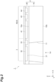
FIG. 5 is a partial plan view inFIGS. 3 and4 . -
FIG. 6 is a sectional view of the solid-state imaging element illustrated inFIG. 1 . -
FIG. 7 is a sectional view of a first element unit of a solid-state imaging element of a second embodiment. -
FIG. 8 is a sectional view of a first element unit of a solid-state imaging element according to a third embodiment. - Hereinafter, embodiments of the present disclosure will be described in detail with reference to the drawings. In the drawings, the same or corresponding portions are denoted by the same reference signs, and redundant portions are omitted.
- As illustrated in
FIGS. 1 and2 , a solid-state imaging element 1 includes asemiconductor substrate 2, afirst element unit 3, and asecond element unit 4. Thefirst element unit 3 and thesecond element unit 4 are formed on asingle semiconductor substrate 2. Thesecond element unit 4 is configured to receive a signal from thefirst element unit 3. Thefirst element unit 3 is, for example, a charge coupled device (CCD) unit, and thesecond element unit 4 is, for example, a complementary metal oxide semiconductor (CMOS) unit. That is, the solid-state imaging element 1 is, for example, a monolithic CCD-CMOS. Hereinafter, a thickness direction of thesemiconductor substrate 2 is referred to as a Z direction, one direction perpendicular to the Z direction is referred to as an X direction, and a direction perpendicular to both directions of the Z direction and the X direction is referred to as a Y direction. - The
semiconductor substrate 2 has, for example, a rectangular shape as viewed from the Z direction. A longitudinal direction of thesemiconductor substrate 2 is along the X direction. Thesemiconductor substrate 2 includes abase portion 10 and asemiconductor layer 20. - The
base portion 10 has a P-type conductivity type. Thebase portion 10 is, for example, a silicon substrate. Thebase portion 10 has asurface 10a and asurface 10b perpendicular to the Z direction. Thesurface 10b has an openedrecessed portion 11. Therecessed portion 11 has, for example, a quadrangular frustum shape expanding from thesurface 10a toward thesurface 10b. In the present embodiment, the recessedportion 11 penetrates thebase portion 10. Accordingly, thesemiconductor layer 20 is exposed at a bottom portion of the recessedportion 11. The recessedportion 11 is formed by, for example, etching. A thickness of the portion of thebase portion 10 where the recessedportion 11 is not formed is, for example, about 300 µm. - The
semiconductor layer 20 is formed on thesurface 10a of thebase portion 10. Thesemiconductor layer 20 is, for example, an epitaxial growth layer containing silicon. A thickness of thesemiconductor layer 20 is, for example, about 10 µm. Thefirst element unit 3 and thesecond element unit 4 are formed in thesemiconductor layer 20. - The
first element unit 3 includes alight receiving part 31, atransfer part 32, and anamplifier part 33. Thelight receiving part 31 generates charges in response to incidence of light hv. Thelight receiving part 31 is formed at a position overlapping the recessedportion 11 in the Z direction. The light hv is incident on thelight receiving part 31 from thesurface 10b side of thebase portion 10 via the recessedportion 11. Thelight receiving part 31 includes, for example, a plurality of pixels aligned two-dimensionally along the X direction and the Y direction. Thetransfer part 32 transfers the charges generated in thelight receiving part 31. Thetransfer part 32 transfers the charges along the X direction for each pixel array extending along the X direction. Theamplifier part 33 converts the charge transferred by thetransfer part 32 into an analog signal (signal voltage). Theamplifier part 33 is electrically connected to thetransfer part 32 by a wiring W1. The analog signal converted by theamplifier part 33 is transmitted to thesecond element unit 4. - The
second element unit 4 includes asignal processing part 40. Thesignal processing part 40 processes a digital signal corresponding to the charge transferred by thetransfer part 32. Thesignal processing part 40 includes aconversion part 41, adrive part 42, amultiplexer part 43, and anoutput part 44. Theconversion part 41 converts the analog signal received from thefirst element unit 3 into a digital signal. Theconversion part 41 is electrically connected to theamplifier part 33 by a wiring W2. Thedrive part 42 generates a signal for driving theconversion part 41. Thedrive part 42 includes, for example, a phase locked loop (PLL) and a timing generator. Thedrive part 42 is electrically connected to theconversion part 41 by a wiring W3. Themultiplexer part 43 bundles a plurality of digital signals converted by theconversion part 41 to generate one digital signal. Themultiplexer part 43 is electrically connected to theconversion part 41 by a wiring W4. Theoutput part 44 converts the digital signal from themultiplexer part 43 into a differential voltage signal and outputs the differential voltage signal to an outside. Theoutput part 44 includes, for example, a low voltage differential signaling (LVDS) part. Theoutput part 44 is electrically connected to themultiplexer part 43 by a wiring W5. - As illustrated in
FIGS. 3 ,4 , and5 , thesemiconductor layer 20 includes asemiconductor region 21, asemiconductor region 22, and a plurality ofsemiconductor regions 23. Thesemiconductor region 21 has a P-type conductivity type, and is formed on thesurface 10a of thebase portion 10. Thesemiconductor region 22 has an N-type conductivity type, and is formed on thesemiconductor region 21. Eachsemiconductor region 23 has an N--type conductivity type. The "N--type" means that a concentration of an N-type impurity is lower than that of the "N-type". Eachsemiconductor region 23 is formed within thesemiconductor region 22 along a surface of thesemiconductor region 22 opposite to thesemiconductor region 21. - The
light receiving part 31 includes a PN junction region formed in thesemiconductor layer 20. Specifically, the PN junction region is formed at a boundary portion between thesemiconductor region 21 and thesemiconductor region 22. When the light hv is incident on the PN junction region formed in thesemiconductor layer 20, the charges are generated. - The
transfer part 32 includes acharge transfer region 70, acharge discharge region 75, a plurality oftransfer electrodes 80, adischarge gate electrode 85, and a plurality of insulatinglayers 90. Thecharge transfer region 70 is formed within thesemiconductor layer 20. Thecharge transfer region 70 includes thesemiconductor region 22 and thesemiconductor region 23, and transfers the charge generated in thelight receiving part 31. Thecharge transfer region 70 includes a plurality offirst transfer regions 71 and a plurality ofsecond transfer regions 72. Thefirst transfer region 71 of the present embodiment is a region positioned between twosemiconductor regions 22 aligned in the X direction in thesemiconductor region 23, and overlaps afirst transfer electrode 81 to be described later in the Z direction. Thefirst transfer region 71 does not include thesemiconductor region 23. Thesecond transfer region 72 of the present embodiment is a region including thesemiconductor region 23, and overlaps asecond transfer electrode 82 to be described later in the Z direction. Thefirst transfer region 71 and thesecond transfer region 72 are alternately aligned in a transfer direction of the charges (X direction). Thesemiconductor region 22 has an N-type conductivity type, and thesemiconductor region 23 has an N--type conductivity type. Accordingly, an impurity concentration of thefirst transfer region 71 not including thesemiconductor region 23 is different from an impurity concentration of thesecond transfer region 72 including thesemiconductor region 23. Specifically, the impurity concentration of thefirst transfer region 71 is higher than the impurity concentration of thesecond transfer region 72. - The plurality of
transfer electrodes 80 are disposed over thecharge transfer region 70 and includes a plurality offirst transfer electrodes 81 and a plurality ofsecond transfer electrodes 82. Thefirst transfer electrode 81 and thesecond transfer electrode 82 are made of, for example, polysilicon. Thefirst transfer electrode 81 and thesecond transfer electrode 82 are electrodes that transfer the charges generated in thelight receiving part 31 in the X direction. Thefirst transfer electrode 81 and thesecond transfer electrode 82 transfer the charges for each pixel array extending along the X direction. Thefirst transfer electrode 81 is disposed over thefirst transfer region 71, and thesecond transfer electrode 82 is disposed over thesecond transfer region 72. Thefirst transfer electrode 81 and thesecond transfer electrode 82 are alternately aligned in the transfer direction of the charges (X direction). - The
first transfer electrode 81 has, for example, a rectangular shape as viewed from the Z direction. A longitudinal direction of thefirst transfer electrode 81 is along the Y direction. A shape of thefirst transfer electrode 81 as viewed from the Z direction is not limited. Thefirst transfer electrode 81 has a flat plate shape along the X direction and the Y direction. Thefirst transfer electrode 81 has a pair ofsurfaces surfaces surface 81a is positioned farther from thesemiconductor substrate 2 than thesurface 81b. As viewed from the Z direction, thefirst transfer electrode 81 has a pair of overlapping portions A1 overlapping a part (overlapping portion A2) of thesecond transfer electrode 82. The pair of overlapping portions A1 is positioned at both end portions of thefirst transfer electrode 81 in the X direction. - The
second transfer electrode 82 has, for example, a rectangular shape as viewed from the Z direction. A longitudinal direction of thesecond transfer electrode 82 is along the Y direction. A shape of thesecond transfer electrode 82 as viewed from the Z direction is not limited. Thesecond transfer electrode 82 includes afirst portion 83 and a pair ofsecond portions 84. Thefirst portion 83 has a flat shape along the X direction and the Y direction. Thefirst portion 83 is spaced apart from thesemiconductor layer 20 by the same distance as a distance from thesemiconductor layer 20 to thefirst transfer electrode 81. Thefirst portion 83 has a pair ofsurfaces surface 83b is positioned closer to thesemiconductor layer 20 than thesurface 83a, and is at the same height as thesurface 81b of thefirst transfer electrode 81. Thesecond portion 84 is positioned farther from thesemiconductor layer 20 than thefirst portion 83 in the Z direction. Thesecond portion 84 is formed to be bent from the Z direction to the X direction in XZ sectional view. Thesecond portion 84 has a portion along the Y direction and the Z direction and a portion along the X direction and the Y direction. The portion of thesecond portion 84 along the Y direction and the Z direction is continuous with corresponding an end portion of both end portions of thefirst portion 83 in the X direction. Thesecond portion 84 has an overlapping portion A2. The overlapping portion A2 is a portion overlapping the overlapping portion A1 of thefirst transfer electrode 81 as viewed from the Z direction. The overlapping portion A2 is positioned on thesurface 81a side with respect to thefirst transfer electrode 81 in the Z direction. As viewed from the Z direction, a gap is not formed between thefirst transfer electrode 81 and thesecond transfer electrode 82. - The
charge discharge region 75 is a region where the charges are discharged from thecharge transfer region 70. Thecharge discharge region 75 is along thecharge transfer region 70 and is adjacent to thecharge transfer region 70 in the Y direction. Thecharge discharge region 75 includes adrain region 76. Thedrain region 76 is a region from which surplus charges within thecharge transfer region 70 are discharged. Thedrain region 76 extends in the X direction. Thedrain region 76 has an N+-type conductivity type. The "N+-type" means that a concentration of an N-type impurity is higher than that of the "N-type". - The
discharge gate electrode 85 is disposed over thecharge discharge region 75. Thedischarge gate electrode 85 extends in the X direction. That is, thedischarge gate electrode 85 and thedrain region 76 extend in the same direction. Thedischarge gate electrode 85 has, for example, a rectangular shape as viewed from the Z direction. A longitudinal direction of thedischarge gate electrode 85 is along the X direction. A shape of thedischarge gate electrode 85 as viewed from the Z direction is not limited. Thedischarge gate electrode 85 includes afirst portion 86 and asecond portion 87. Thefirst portion 86 has a flat shape along the X direction and the Y direction. Thefirst portion 86 is spaced apart from thesemiconductor layer 20 by the same distance as the distance from thesemiconductor layer 20 to thefirst transfer electrode 81. Of a pair ofsurfaces first portion 86, thesurface 86b closer to thesemiconductor layer 20 is at the same height as thesurface 81b of thefirst transfer electrode 81. Thefirst portion 86 overlaps thedrain region 76 in the Z direction. Thesecond portion 87 is positioned farther from thesemiconductor layer 20 than thefirst portion 86 in the Z direction. Thesecond portion 87 is formed to be bent from the Z direction to the Y direction in YZ sectional view. Thesecond portion 87 has a portion along the X direction and the Z direction and a portion along the X direction and the Y direction. The portion of thesecond portion 87 along the X direction and the Z direction is continuous with an end portion on thecharge transfer region 70 side of both end portions of thefirst portion 86 in the Y direction. - As viewed from the Z direction, the
first transfer electrode 81 has an overlapping portion A3 overlapping a part (overlapping portion A4) of thedischarge gate electrode 85. The overlapping portion A3 is positioned at an end portion on thecharge discharge region 75 side of both end portions of thefirst transfer electrode 81 in the Y direction. Thesecond portion 87 of thedischarge gate electrode 85 has an overlapping portion A4. The overlapping portion A4 is a portion overlapping the overlapping portion A3 of thefirst transfer electrode 81 as viewed from the Z direction. The overlapping portion A4 is positioned on thesurface 81a side with respect to thefirst transfer electrode 81 in the Z direction. Accordingly, the overlapping portion A2 of thesecond transfer region 72 and the overlapping portion A4 of thedischarge gate electrode 85 are positioned on the same side with respect to thefirst transfer electrode 81 in the Z direction. As viewed from the Z direction, a gap is not formed between thefirst transfer electrode 81 and thedischarge gate electrode 85. Thedischarge gate electrode 85 extends over the plurality offirst transfer electrodes 81 aligned spaced apart in the X direction. That is, the commondischarge gate electrode 85 extends to overlap the plurality offirst transfer electrodes 81. - As viewed from the Z direction, the
second transfer electrode 82 is spaced apart from thedischarge gate electrode 85. That is, as viewed from the Z direction, a gap is formed between thesecond transfer electrode 82 and thedischarge gate electrode 85. In the present embodiment, thesecond transfer electrode 82 is spaced apart from thedischarge gate electrode 85 in the Y direction. As viewed from the Z direction, a width of the gap between thedischarge gate electrode 85 and thesecond transfer electrode 82 in the Y direction is smaller than an interval between thefirst transfer electrodes 81 adjacent in the X direction. Thesecond transfer electrode 82 is not in contact with thedischarge gate electrode 85 and does not overlap thedischarge gate electrode 85 in the Z direction. - A layer structure of the electrodes (
first transfer electrode 81,second transfer electrode 82, and discharge gate electrode 85) included in the solid-state imaging element 1 has a two-layer structure. In the solid-state imaging element 1, thefirst transfer electrode 81 is formed as a first layer, and thesecond transfer electrode 82 and thedischarge gate electrode 85 are formed as second layers different from the first layer. The "first layer" and the "second layer" correspond to timings at which layers are formed in ae manufacturing process of the solid-state imaging element 1. Specifically, the layer formed as the first layer is a layer that cannot be formed simultaneously with the layer formed as the second layer. In the present embodiment, since a part of thefirst transfer electrode 81 overlaps thesecond transfer electrode 82 and thedischarge gate electrode 85, thefirst transfer electrode 81 cannot be formed simultaneously with thesecond transfer electrode 82 and thedischarge gate electrode 85. Thefirst transfer electrode 81 is formed before the formation of thesecond transfer electrode 82 and thedischarge gate electrode 85. In addition, layers formed as the same layer can be simultaneously formed. In the present embodiment, thesecond transfer electrode 82 and thedischarge gate electrode 85 formed as the same second layer are simultaneously formed after thefirst transfer electrode 81 is formed. The layers formed as the same layer may be layers that can be simultaneously formed, and may not necessarily be simultaneously formed. For example, in the present embodiment, thesecond transfer electrode 82 and thedischarge gate electrode 85 may be formed at different timings. - The plurality of insulating
layers 90 are formed on thesemiconductor layer 20. Each insulatinglayer 90 is a layer made of, for example, silicon oxide. The silicon oxide is, for example, SiO2. A thickness of each insulatinglayer 90 is, for example, about several tens to several hundreds nm. The plurality of insulatinglayers 90 electrically separate thefirst transfer electrode 81, thesecond transfer electrode 82, and thedischarge gate electrode 85 from each other. InFIGS. 3 and4 , only an insulatinglayer 91 among the plurality of insulatinglayers 90 is indicated by a dashed double-dotted line for the sake of convenience in description. The insulatinglayer 91 extends, as the same layer, between the overlapping portion A1 of thefirst transfer electrode 81 and the overlapping portion A2 of thesecond transfer electrode 82 and between the overlapping portion A3 of thefirst transfer electrode 81 and the overlapping portion A4 of thedischarge gate electrode 85. The insulatinglayer 91 is continuously formed along thesurface 81a of thefirst transfer electrode 81 to extend from between the overlapping portion A1 and the overlapping portion A2 to between the overlapping portion A3 and the overlapping portion A4. - A relationship between a layer structure of electrodes of the
first element unit 3 and a layer structure of electrodes of thesecond element unit 4 will be described with reference toFIG. 6 . As illustrated inFIG. 6 , thesecond element unit 4 includes afirst electrode 101, asecond electrode 102, and a plurality ofthird electrodes 103 formed on thesemiconductor layer 20. Thefirst electrode 101, thesecond electrode 102, and the plurality ofthird electrodes 103 are included in the signal processing part 40 (seeFIG. 1 ) of thesecond element unit 4, and are included, for example, in any of theconversion part 41, thedrive part 42, themultiplexer part 43, and theoutput part 44. Thefirst electrode 101, thesecond electrode 102, and the plurality ofthird electrodes 103 are made of, for example, polysilicon. Thefirst electrode 101 and thesecond electrode 102 overlap each other in the Z direction, and constitute, for example, a capacitor. The plurality ofthird electrodes 103 are aligned in the X direction, and constitute, for example, a gate electrode of a field effect transistor (FET). - The
first electrode 101 is formed as the first layer. That is, thefirst electrode 101 can be formed simultaneously with thefirst transfer electrode 81 of thefirst element unit 3. Thefirst electrode 101 is spaced apart from thesemiconductor layer 20 by the same distance as the distance from thesemiconductor layer 20 to thefirst transfer electrode 81. Thesecond electrode 102 is formed as a second layer. That is, thesecond electrode 102 can be formed simultaneously with thesecond transfer electrode 82 of thefirst element unit 3. Thesecond electrode 102 is spaced apart from thesemiconductor layer 20 by the same distance as the distance from thesemiconductor layer 20 to thesecond portion 84 of thesecond transfer electrode 82. Similarly to the electrode (first transfer electrode 81,second transfer electrode 82, and discharge gate electrode 85) of thefirst element unit 3, thefirst electrode 101 and thesecond electrode 102 of thesecond element unit 4 have a two-layer structure. Thethird electrode 103 is spaced apart from thesemiconductor layer 20 by the same distance as the distance from thesemiconductor layer 20 to thefirst transfer electrode 81. Thethird electrode 103 may be formed simultaneously with thefirst electrode 101 or thesecond electrode 102. - The
second element unit 4 has a plurality of insulatinglayers 95 formed on thesemiconductor layer 20. The insulatinglayer 95 is formed integrally with the insulatinglayer 90 of thefirst element unit 3. Each insulatinglayer 95 is a layer made of, for example, silicon oxide. The silicon oxide is, for example, SiO2. The plurality of insulatinglayers 95 electrically separate thefirst electrode 101, thesecond electrode 102, and thethird electrode 103 from each other. InFIG. 6 , only an insulatinglayer 96 among the plurality of insulatinglayers 90 is indicated by a dashed double-dotted line for the sake of convenience in description. The insulatinglayer 96 is formed from between thefirst electrode 101 and thesecond electrode 102 to thethird electrode 103. The insulatinglayer 96 is continuous with the insulatinglayer 91 included in thefirst element unit 3, and can be formed simultaneously with the insulatinglayer 91. That is, the insulating layer positioned between the electrode formed as the first layer and the electrode formed as the second layer in thesecond element unit 4 can be formed simultaneously with the insulating layer positioned between the electrode formed as the first layer and the electrode formed as the second layer in thefirst element unit 3. - A thickness of a
portion 96a of the insulatinglayer 96 positioned between thefirst electrode 101 and thesecond electrode 102 is equal to a thickness of aportion 91a of the insulatinglayer 91 positioned between the overlapping portion A1 of thefirst transfer electrode 81 and the overlapping portion A2 of thesecond transfer electrode 82. - An example of an operation of the solid-
state imaging element 1 having the above configuration will be described. In the solid-state imaging element 1, when the light hv is incident on thelight receiving part 31, the charges are generated in each pixel of thelight receiving part 31. The charges are transferred to theamplifier part 33 by thetransfer part 32. In the present embodiment, the charges are transferred along the X direction from a left side to a right side inFIG. 3 . Here, the transfer method of the charges will be described with reference toFIG. 3 . In the present embodiment, a two-phase driving method is used as the charge transfer method. In the following description, thefirst transfer regions 71 illustrated inFIG. 3 are referred to as first transfer regions 71A and 71B, and thesecond transfer regions 72 are referred to as second transfer regions 72A and 72B. In addition, thefirst transfer electrode 81 over the first transfer region 71A is referred to as a first transfer electrode 81A, and thefirst transfer electrode 81 over the first transfer region 71B is referred to as a first transfer electrode 81B. Similarly, thesecond transfer electrode 82 over the second transfer region 72A is referred to as a second transfer electrode 82A, and thesecond transfer electrode 82 over the second transfer region 72B is referred to as a second transfer electrode 82B. - First, values of voltages P1 applied to the first transfer electrode 81A and the second transfer electrode 82A are increased to appropriate values. The first transfer region 71A has an impurity concentration higher than that of the second transfer region 72A. Thus, in a state where the voltages P1 having the same magnitude are applied to the first transfer electrode 81A and the second transfer electrode 82A, a potential well formed under the first transfer electrode 81A is deeper than a potential well formed under the second transfer electrode 82A. Due to this potential difference, the charges generated in the
light receiving part 31 flow from the second transfer region 72A into the first transfer region 71A and are stored in the first transfer region 71A. That is, the first transfer region 71A functions as a storage that stores the charges. The otherfirst transfer regions 71 similarly function as storages. In contrast, since the potential well under the second transfer electrode 82A is shallower than the potential well under the first transfer electrode 81A, the charges do not flow back from the first transfer region 71A to the second transfer region 72A. That is, the second transfer region 72A functions as a barrier that prevents a backflow of the charges. The othersecond transfer regions 72 similarly function as barriers. - Subsequently, while the values of the voltage P1 applied to the first transfer electrode 81A and the second transfer electrode 82A are decreased, values of voltages P2 applied to the first transfer electrode 81B and the second transfer electrode 82B are increased to appropriate values. As a result, potential wells under the first transfer electrode 81B and the second transfer electrode 82B become deeper than the potential well under the first transfer electrode 81A. In the present embodiment, since the first transfer region 71B has an impurity concentration higher than that of the second transfer region 72B, the potential well under the first transfer electrode 81B is deeper than the potential well under the second transfer electrode 82B. Accordingly, in a state where the value of the voltage P2 is higher than the value of the voltage P1, a depth of the potential well gradually becomes deeper from the first transfer region 71A toward the first transfer region 71B. As a result, the charges stored in the first transfer region 71A pass through the second transfer region 72B and are transferred to the first transfer region 71B. Hereinafter, the charges are transferred in the X direction by repeating the above transfer method also in the other
first transfer electrodes 81 andsecond transfer electrodes 82. - In the solid-
state imaging element 1, the charges may be discharged from thecharge transfer region 70 to thecharge discharge region 75. For example, in a case where excessive charges are present in thecharge transfer region 70 due to the incidence of the strong light hv on thelight receiving part 31, a part of the charges is discharged to thedrain region 76 of thecharge discharge region 75. A discharge method of the charges will be described with reference toFIG. 4 . When the charges are discharged to thecharge discharge region 75, a value of a voltage P3 applied to thedischarge gate electrode 85 is increased to an appropriate value. As a result, a potential well under thedischarge gate electrode 85 becomes deep (the potential barrier becomes low), and the charges are discharged from thecharge transfer region 70 to thecharge discharge region 75. In particular, thedrain region 76 has an N+-type conductivity type and has a high impurity concentration. Thus, when the value of the voltage P3 is increased, a potential well having a relatively large depth is formed in thedrain region 76. Thus, in the present embodiment, the charges discharged to thecharge discharge region 75 mainly flow into thedrain region 76. - The charges transferred in the X direction by the
first transfer electrode 81 and thesecond transfer electrode 82 are sent to theamplifier part 33. In the present embodiment, the charges are sent to theamplifier part 33 for each pixel array extending along the X direction. The electric charge is converted into an analog signal in theamplifier part 33. The analog signal converted by theamplifier part 33 is converted into a digital signal by theconversion part 41. The plurality of digital signals converted by theconversion part 41 are bundled in themultiplexer part 43 and are generated as one digital signal. This digital signal is converted into a differential voltage signal in theoutput part 44 and is output to the outside. - As described above, in the solid-
state imaging element 1, as viewed from the thickness direction of thesemiconductor substrate 2, thefirst transfer electrode 81 includes the overlapping portion A1 overlapping the overlapping portion A2 of thesecond transfer electrode 82 and the overlapping portion A3 overlapping the overlapping portion A4 of thedischarge gate electrode 85. As a result, it is less likely to form gaps between thefirst transfer electrode 81 and thesecond transfer electrode 82 and between thefirst transfer electrode 81 and thedischarge gate electrode 85 as viewed from the thickness direction of thesemiconductor substrate 2. Thus, in thecharge transfer region 70 and thecharge discharge region 75, it is possible to suppress generation of a region where charges are trapped, and it is possible to appropriately perform the transfer of the charges and the discharge of the charges. In addition, in the solid-state imaging element 1 in which thefirst element unit 3 and thesecond element unit 4 are formed on thesingle semiconductor substrate 2, in a case where the layer structure of the electrodes included in thefirst element unit 3 is three or more layers, it is less likely to form the electrodes and the like included in thesecond element unit 4 with high accuracy. For example, in a case where the layer structure of the electrode included in thefirst element unit 3 is three or more layers, a step is generated between thefirst element unit 3 and thesecond element unit 4, and a resolution when the electrode or the like of thesecond element unit 4 is formed by photolithography is reduced. In contrast, in the solid-state imaging element 1, the layer structure of thefirst transfer electrode 81, thesecond transfer electrode 82, and thedischarge gate electrode 85 included in thefirst element unit 3 is two layers. Thus, the step is hardly generated between thefirst element unit 3 and thesecond element unit 4, and it is possible to form an electrode or the like included in thesecond element unit 4 with high accuracy. As described above, according to the solid-state imaging element 1, appropriate characteristics can be secured. - Further, in the solid-
state imaging element 1, as viewed from the Z direction, thefirst transfer electrode 81 disposed over thefirst transfer region 71 functioning as the storage overlaps thedischarge gate electrode 85, and thesecond transfer electrode 82 disposed over thesecond transfer region 72 functioning as the barrier does not overlap thedischarge gate electrode 85. As a result, the charges are efficiently discharged from thefirst transfer region 71 in which more charges are stored than in thesecond transfer region 72 to thecharge discharge region 75, and it is possible to avoid the layer structure of the electrodes (first transfer electrode 81,second transfer electrode 82, and discharge gate electrode 85) included in thefirst element unit 3 from having a three-layer structure. - Further, in the solid-
state imaging element 1, the overlapping portion A1 of thefirst transfer electrode 81 and the overlapping portion A2 of thesecond transfer electrode 82 overlap each other, and thus, the generation of the region where the charges are trapped is suppressed. Thus, in the solid-state imaging element 1, it is not necessary to excessively narrow an interval between thefirst transfer electrode 81 and thesecond transfer electrode 82 within an XY plane (specifically, an interval between thefirst transfer electrode 81 and thefirst portion 83 of the second transfer electrode 82) in order to suppress the generation of the region where the charges are trapped. For the same reason, in the solid-state imaging element 1, it is not necessary to excessively narrow an interval between thefirst transfer electrode 81 and thedischarge gate electrode 85 in the XY plane (specifically, an interval between thefirst transfer electrode 81 and thefirst portion 86 of the discharge gate electrode 85) in order to suppress the generation of the region where the charge is trapped. Thus, according to the solid-state imaging element 1, it is possible to suppress short circuits between thefirst transfer electrode 81 and thesecond transfer electrode 82 and between thefirst transfer electrode 81 and thedischarge gate electrode 85, and appropriate characteristics can be secured. - Further, in a solid-state imaging element having a three-layer layer structure in which the discharge gate electrode is formed as the first layer, the first transfer electrode is formed as the second layer to overlap a part of the discharge gate electrode, and the second transfer electrode is formed as the third layer to overlap a part of the discharge gate electrode and a part of the first transfer electrode, the first transfer electrode does not have a flat shape. Specifically, the first transfer electrode rides over the discharge gate electrode, and has a hollow due to a thickness of the discharge gate electrode. In a case where the first transfer electrode has the hollow, when the second transfer electrode is formed, a material of the second transfer electrode that has entered the hollow of the first transfer electrode may remain as a residue without being removed by etching. This residue may cause a short circuit between the second transfer electrodes. In contrast, in the solid-
state imaging element 1, thefirst transfer electrode 81 has a flat shape. Thus, in the solid-state imaging element 1, the material of thesecond transfer electrode 82 hardly remains as the residue on thefirst transfer electrode 81, and the short circuit between thesecond transfer electrodes 82 can be suppressed. Accordingly, according to the solid-state imaging element 1, appropriate characteristics can be secured. - In the solid-
state imaging element 1, the overlapping portion A2 of thesecond transfer electrode 82 and the overlapping portion A4 of thedischarge gate electrode 85 are positioned on the same side with respect to thefirst transfer electrode 81 in the thickness direction of thesemiconductor substrate 2. According to this configuration, the layer structure of thefirst transfer electrode 81, thesecond transfer electrode 82, and thedischarge gate electrode 85 included in thefirst element unit 3 can be formed into two layers with a simple structure. - In the solid-
state imaging element 1, thetransfer part 32 further includes the insulatinglayer 91 extending as the same layer between thefirst transfer electrode 81 and the overlapping portion A2 of thesecond transfer electrode 82 and between thefirst transfer electrode 81 and the overlapping portion A4 of thedischarge gate electrode 85. According to this configuration, the layer structure of thefirst transfer electrode 81, thesecond transfer electrode 82, and thedischarge gate electrode 85 included in thefirst element unit 3 can be formed into two layers with a simple structure. - In the solid-
state imaging element 1, thecharge discharge region 75 includes thedrain region 76, and thedischarge gate electrode 85 and thedrain region 76 extend in the transfer direction (X direction). According to this configuration, the surplus charges in thecharge transfer region 70 can be appropriately discharged to thedrain region 76, and an anti-blooming property of the solid-state imaging element 1 can be improved. - In the solid-
state imaging element 1, thefirst element unit 3 includes theamplifier part 33 that converts the charge transferred by thetransfer part 32 into the analog signal, and thesecond element unit 4 includes theconversion part 41 that converts the analog signal into the digital signal. According to this configuration, the solid-state imaging element 1 can convert the analog signal into the digital signal that is not easily influenced by noise. - In the solid-
state imaging element 1, thecharge transfer region 70 includes thefirst transfer region 71 and thesecond transfer region 72 having the impurity concentration different from that of thefirst transfer region 71, thefirst transfer electrode 81 is disposed over thefirst transfer region 71, and thesecond transfer electrode 82 is disposed over thesecond transfer region 72. According to this configuration, the two-phase driving method can be used as the charge transfer method in thetransfer part 32, and the operation of thefirst element unit 3 can be realized with a control voltage of a minimum number of phases (two phases). - A
first element unit 3A included in a solid-state imaging element 1 of a second embodiment is different from the solid-state imaging element 1 of the first embodiment described above in that thesemiconductor region 23 is not formed and a three-phase driving method is used as the charge transfer method. - As illustrated in
FIG. 7 , thesemiconductor region 23 is not formed in thesemiconductor layer 20. Accordingly, in thefirst element unit 3A, the impurity concentration of thefirst transfer region 71 is not different from the impurity concentration of thesecond transfer region 72. In the second embodiment, the region of thesemiconductor regions 22 positioned immediately below thefirst transfer electrode 81 corresponds to thefirst transfer region 71, and a region of thesemiconductor regions 22 positioned between two thefirst transfer regions 71 aligned in the X direction corresponds to thesecond transfer region 72. - A transfer method of charges in the
first element unit 3A will be described. In the present embodiment, the three-phase driving method is used as the charge transfer method in thetransfer part 32. In the three-phase driving method, charge transfer is performed by applying the same voltage to every three electrodes. In the following description, onefirst transfer region 71 among the plurality offirst transfer regions 71 illustrated inFIG. 7 is referred to as the first transfer region 71A, and thesecond transfer regions 72 aligned to sandwich the first transfer region 71A in the X direction are referred to as second transfer regions 72A and 72B. In addition, thefirst transfer electrode 81 over the first transfer region 71A is referred to as a first transfer electrode 81A. Similarly, thesecond transfer electrode 82 over the second transfer region 72A is referred to as the second transfer electrode 82A, and thesecond transfer electrode 82 over the second transfer region 72B is referred to as the second transfer electrode 82B. - First, a value of a voltage P11 applied to the second transfer electrode 82A is increased to an appropriate value. As a result, the potential well under the second transfer electrode 82A becomes deep, and the charges generated in the
light receiving part 31 are stored in the second transfer region 72A. Subsequently, while the value of the voltage P11 is maintained, a value of a voltage P12 applied to the first transfer electrode 81A is increased to the same level as the value of the voltage P11. As a result, the potential well under the first transfer electrode 81A becomes deep, and the charges stored in the second transfer region 72A also flow into the first transfer region 71A. In this state, the value of the voltage P11 is reduced. As a result, the potential well under the second transfer electrode 82A becomes shallow, and all the charges stored in the second transfer region 72A are transferred to the first transfer region 71A. - Subsequently, while the value of the voltage P12 is maintained, a value of a voltage P13 applied to the second transfer electrode 82B is increased to the same level as the value of the voltage P12. As a result, the potential well under the second transfer electrode 82B becomes deep, and the charges stored in the first transfer region 71A also flow into the second transfer region 72B. In this state, the value of the voltage P12 is reduced. As a result, the potential well under the first transfer electrode 81A becomes shallow, and all the charges stored in the first transfer region 71A are transferred to the second transfer region 72B. Hereinafter, the charges are transferred to the
amplifier part 33 by repeating the above-described transfer method also in the otherfirst transfer electrodes 81 andsecond transfer electrodes 82. - As in the first embodiment, in the second embodiment, the appropriate characteristics of the solid-
state imaging element 1 can also be secured. In addition, in the second embodiment, the three-phase driving method is used as the charge transfer method. As a result, in the second embodiment, since it is not necessary to set the impurity concentrations of thefirst transfer region 71 and thesecond transfer region 72 to be different from each other (since it is not necessary to form thesemiconductor region 23 in the semiconductor region 22), thefirst element unit 3A can be more easily formed. - A
first element unit 3B included in a solid-state imaging element 1 of a third embodiment is different from the solid-state imaging element 1 of the first embodiment described above in that thesemiconductor region 23 is not formed and that a four-phase driving method is used as the charge transfer method. - As illustrated in
FIG. 8 , thesemiconductor region 23 is not formed in thesemiconductor layer 20. Accordingly, in thefirst element unit 3B, the impurity concentration of thefirst transfer region 71 is not different from the impurity concentration of thesecond transfer region 72. As in the second embodiment, in the third embodiment, the region of thesemiconductor regions 22 positioned immediately below thefirst transfer electrode 81 corresponds to thefirst transfer region 71, and the region of thesemiconductor regions 22 positioned between twofirst transfer regions 71 aligned in the X direction corresponds to thesecond transfer region 72. - A transfer method of charges in the
first element unit 3B will be described. In the present embodiment, the four-phase driving method is used as the charge transfer method in thetransfer part 32. In the four-phase driving method, charge transfer is performed by applying the same voltage for every four electrodes. In the following description, among the plurality offirst transfer regions 71 illustrated inFIG. 8 , twofirst transfer regions 71 aligned in the X direction are referred to as the first transfer regions 71A and 71B, and thesecond transfer regions 72 aligned to sandwich the first transfer region 71A in the X direction are referred to as the second transfer regions 72A and 72B. In addition, thefirst transfer electrode 81 over the first transfer region 71A is referred to as the first transfer electrode 81A, and thefirst transfer electrode 81 over the first transfer region 71B is referred to as the first transfer electrode 81B. Similarly, thesecond transfer electrode 82 over the second transfer region 72A is referred to as the second transfer electrode 82A, and thesecond transfer electrode 82 over the second transfer region 72B is referred to as the second transfer electrode 82B. - First, a value of a voltage P21 applied to the second transfer electrode 82A and a value of a voltage P22 applied to the first transfer electrode 81A are increased to appropriate values. As a result, the potential wells under the second transfer electrode 82A and the first transfer electrode 81A becomes deep, and the charges generated in the
light receiving part 31 are stored in the second transfer region 72A and the first transfer region 71A. Subsequently, while the values of the voltages P21 and P22 are maintained, a value of a voltage P23 applied to the second transfer electrode 82B is increased to the same level as the values of the voltages P21 and P22. As a result, the potential well under the second transfer electrode 82B becomes deep, and the charges stored in the second transfer region 72A and the first transfer region 71A also flow into the second transfer region 72B. In this state, the value of the voltage P21 is reduced. As a result, the potential well under the second transfer electrode 82A becomes shallow, and all the charges stored in the second transfer region 72A are transferred to the first transfer region 71A and the second transfer region 72B. - Subsequently, while the values of the voltages P22 and P23 are maintained, a value of a voltage P24 applied to the first transfer electrode 81B is increased to the same level as the values of the voltages P22 and P23. As a result, the potential well under the first transfer electrode 81B becomes deep, and the charges stored in the first transfer region 71A and the second transfer region 72B also flow into the first transfer region 71B. In this state, the value of the voltage P22 is reduced. As a result, the potential well under the first transfer electrode 81A becomes shallow, and all the charges stored in the first transfer region 71A are transferred to the second transfer region 72B and the first transfer region 71B. Hereinafter, the charges are transferred to the
amplifier part 33 by repeating the above-described transfer method also in the otherfirst transfer electrodes 81 andsecond transfer electrodes 82. - As in the first embodiment, in the third embodiment, the appropriate characteristics of the solid-
state imaging element 1 can also be secured. In addition, in the third embodiment, the four-phase driving method is used as the charge transfer method. As a result, in the third embodiment, since it is not necessary to set the impurity concentrations of thefirst transfer region 71 and thesecond transfer region 72 to be different from each other (since it is not necessary to form thesemiconductor region 23 in the semiconductor region 22), thefirst element unit 3B can be more easily formed. - The present disclosure is not limited to the above embodiments. In the solid-
state imaging element 1 of the above embodiments, the P-type and N-type conductivity types may be opposite to those described above. For example, thesemiconductor region 22 may have a P-type conductivity type, and thesemiconductor region 23 may have a P+-type conductivity type. The "P+-type" means that a concentration of a P-type impurity is higher than that of the "P-type". - In addition, the overlapping portion A2 of the
second transfer electrode 82 and the overlapping portion A4 of thedischarge gate electrode 85 may be positioned on thesurface 81b side with respect to thefirst transfer electrode 81 in the thickness direction (Z direction) of thesemiconductor substrate 2. In this case, thesecond portion 84 of thesecond transfer electrode 82 and thesecond portion 87 of thedischarge gate electrode 85 are positioned to enter between thefirst transfer electrode 81 and thesemiconductor layer 20. In the present modification, in the manufacturing process of the solid-state imaging element 1, thefirst transfer electrode 81 as the first layer is formed after thesecond transfer electrode 82 and thedischarge gate electrode 85 as the second layers are formed. Accordingly, an order of forming the first layer and the second layer is not limited. - In addition, in the above embodiments, the
discharge gate electrode 85 is an electrode to which a voltage P3 having any value can be applied at any timing. That is, in the above embodiments, thedischarge gate electrode 85 functions as a shutter electrode that controls a height of a potential barrier between thecharge transfer region 70 and thecharge discharge region 75. However, thedischarge gate electrode 85 may be an electrode to which a constant voltage is constantly applied. In this case, in a case where the amount of charges in thecharge transfer region 70 exceeds a predetermined threshold value, the charges are discharged from thecharge transfer region 70 to thecharge discharge region 75. That is, thedrain region 76 functions as an overflow drain region. - In addition, the charges discharged from the
charge transfer region 70 to thecharge discharge region 75 may be transferred to a region other than thedrain region 76 and used without flowing into thedrain region 76. - In addition, in the above embodiments, a full frame transfer (FFT) method has been described as an example of the method for transferring the charges generated in the
light receiving part 31, but the method for transferring the charges may be, for example, a frame transfer (FT) method, an inter-line (IT) method, or the like. In a case where the full frame transfer method or the frame transfer method is adopted as the charge transfer method, the region of thesemiconductor layer 20 constituting thelight receiving part 31 also functions as thetransfer part 32. In contrast, in a case where the inter-line (IT) method is adopted as the charge transfer method, a region different from the region of thesemiconductor layer 20 constituting thelight receiving part 31 functions as thetransfer part 32. - In addition, in the above embodiments, the back-side incidence type solid-
state imaging element 1 in which the light hv is incident from thesurface 10b side of thebase portion 10 has been described as an example, but the solid-state imaging element 1 may be a front-side incidence type solid-state imaging element in which the light hv is incident from thetransfer electrode 80 side. In addition, thebase portion 10 may not have the recessedportion 11, and the entire thickness of thebase portion 10 may be uniform. - The distance from the
semiconductor layer 20 to thefirst transfer electrode 81 may be different from a distance from thesemiconductor layer 20 to thefirst portion 83 of thesecond transfer electrode 82. That is, a height of thesurface 81b of thefirst transfer electrode 81 in the Z direction may be different from a height of thesurface 83b of thefirst portion 83. In addition, the distance from thesemiconductor layer 20 to thefirst transfer electrode 81 may be different from a distance from thesemiconductor layer 20 to thefirst portion 86 of thedischarge gate electrode 85. That is, the height of thesurface 81b of thefirst transfer electrode 81 in the Z direction may be different from a height of thesurface 86b of thefirst portion 86. As viewed from the Z direction, the width of the gap between thedischarge gate electrode 85 and thesecond transfer electrode 82 in the Y direction may be larger than or equal to the interval between thefirst transfer electrodes 81 adjacent in the X direction. - The
first transfer electrode 81 of thefirst element unit 3 may be formed at a timing different from that of thefirst electrode 101 of thesecond element unit 4. The distance from thesemiconductor layer 20 to thefirst transfer electrode 81 may be different from a distance from thesemiconductor layer 20 to thefirst electrode 101. In addition, thesecond transfer electrode 82 of thefirst element unit 3 may be formed at a timing different from that of thesecond electrode 102 of thesecond element unit 4. The distance from thesemiconductor layer 20 to thesecond portion 84 of thesecond transfer electrode 82 may be different from a distance from thesemiconductor layer 20 to thesecond electrode 102. Further, the insulatinglayer 91 of thefirst element unit 3 may be formed separately from the insulatinglayer 96 of thesecond element unit 4, or may be formed at a timing different from that of the insulatinglayer 96. The thickness of theportion 91a of the insulatinglayer 91 may be different from the thickness of theportion 96a of the insulatinglayer 96. - The
second element unit 4 may be configured to transmit the signal to thefirst element unit 3. For example, thesecond element unit 4 may include a generation part that generates a drive signal for driving thefirst element unit 3, and the drive signal generated by the generation part may be transmitted to thefirst element unit 3. Thesecond element unit 4 may be configured to perform at least one of transmission of a signal to thefirst element unit 3 and reception of a signal from thefirst element unit 3. -
- 1 solid-state imaging element
- 2 semiconductor substrate
- 3, 3A, 3B first element unit
- 4 second element unit
- 31 light receiving part
- 32 transfer part
- 33 amplifier part
- 40 signal processing part
- 41 conversion part
- 70 charge transfer region
- 71, 71A, 71B first transfer region
- 72, 72A, 72B second transfer region
- 75 charge discharge region
- 76 drain region
- 81, 81A, 81B first transfer electrode
- 82, 82A, 82B second transfer electrode
- 85 discharge gate electrode
- 91 insulating layer
- hv light
Claims (6)
- A solid-state imaging element comprising:a semiconductor substrate;a first element unit formed on the semiconductor substrate; anda second element unit formed on the semiconductor substrate, whereinthe first element unit includes a light receiving part configured to generate charges in response to incidence of light, and a transfer part configured to transfer the charges,the second element unit is configured to perform at least one of transmission of a signal to the first element unit and reception of a signal from the first element unit,the transfer part includesa first transfer electrode and a second transfer electrode that are disposed over a charge transfer region of the semiconductor substrate, and are aligned in a transfer direction of the charges, anda discharge gate electrode that is disposed over a charge discharge region of the semiconductor substrate along the charge transfer region,the first transfer electrode is formed as a first layer,the second transfer electrode and the discharge gate electrode are formed as second layers different from the first layer,as viewed from a thickness direction of the semiconductor substrate, the first transfer electrode includes a portion overlapping a part of the second transfer electrode and a portion overlapping a part of the discharge gate electrode, andas viewed from the thickness direction of the semiconductor substrate, the second transfer electrode is spaced apart from the discharge gate electrode.
- The solid-state imaging element according to claim 1, wherein the part of the second transfer electrode and the part of the discharge gate electrode are positioned on the same side with respect to the first transfer electrode in the thickness direction of the semiconductor substrate.
- The solid-state imaging element according to claim 1 or 2, wherein the transfer part further includes an insulating layer extending as the same layer between the first transfer electrode and the part of the second transfer electrode and between the first transfer electrode and the part of the discharge gate electrode.
- The solid-state imaging element according to any one of claims 1 to 3, whereinthe charge discharge region includes a drain region, andthe discharge gate electrode and the drain region extend in the transfer direction.
- The solid-state imaging element according to any one of claims 1 to 4, whereinthe first element unit includes an amplifier part configured to convert the charge transferred by the transfer part into an analog signal, andthe second element unit includes a conversion part configured to convert the analog signal into a digital signal.
- The solid-state imaging element according to any one of claims 1 to 5, whereinthe charge transfer region includes a first transfer region and a second transfer region having an impurity concentration different from an impurity concentration of the first transfer region,the first transfer electrode is disposed over the first transfer region, andthe second transfer electrode is disposed over the second transfer region.
Applications Claiming Priority (2)
| Application Number | Priority Date | Filing Date | Title |
|---|---|---|---|
| JP2022026499A JP7765306B2 (en) | 2022-02-24 | 2022-02-24 | solid-state imaging device |
| PCT/JP2022/045530 WO2023162407A1 (en) | 2022-02-24 | 2022-12-09 | Solid-state imaging element |
Publications (2)
| Publication Number | Publication Date |
|---|---|
| EP4468359A1 true EP4468359A1 (en) | 2024-11-27 |
| EP4468359A4 EP4468359A4 (en) | 2026-01-07 |
Family
ID=87765565
Family Applications (1)
| Application Number | Title | Priority Date | Filing Date |
|---|---|---|---|
| EP22928924.4A Pending EP4468359A4 (en) | 2022-02-24 | 2022-12-09 | SOLID BODY IMAGE ELEMENT |
Country Status (7)
| Country | Link |
|---|---|
| US (1) | US20250160027A1 (en) |
| EP (1) | EP4468359A4 (en) |
| JP (1) | JP7765306B2 (en) |
| KR (1) | KR20240152310A (en) |
| CN (1) | CN118872063A (en) |
| TW (1) | TW202341720A (en) |
| WO (1) | WO2023162407A1 (en) |
Family Cites Families (12)
| Publication number | Priority date | Publication date | Assignee | Title |
|---|---|---|---|---|
| EP0025658A3 (en) * | 1979-09-18 | 1983-04-20 | The Secretary of State for Defence in Her Britannic Majesty's Government of the United Kingdom of Great Britain and | Improvements in or relating to charge storage and transfer devices and their fabrication |
| JPH07105456B2 (en) * | 1989-06-22 | 1995-11-13 | 株式会社東芝 | Semiconductor integrated circuit and manufacturing method thereof |
| JP4329128B2 (en) * | 1996-07-12 | 2009-09-09 | ソニー株式会社 | Solid-state imaging device, driving method of solid-state imaging device, and camera |
| US6693671B1 (en) * | 2000-03-22 | 2004-02-17 | Eastman Kodak Company | Fast-dump structure for full-frame image sensors with lod antiblooming structures |
| JP4686830B2 (en) | 2000-08-28 | 2011-05-25 | ソニー株式会社 | Solid-state imaging device and driving method thereof |
| US7265397B1 (en) * | 2000-08-30 | 2007-09-04 | Sarnoff Corporation | CCD imager constructed with CMOS fabrication techniques and back illuminated imager with improved light capture |
| JP2005072932A (en) | 2003-08-25 | 2005-03-17 | Link Research Kk | Charge-coupled analog / digital conversion means and imaging device using the same |
| JP4771664B2 (en) | 2004-01-30 | 2011-09-14 | ルネサスエレクトロニクス株式会社 | Solid-state imaging device and driving method thereof |
| JP2006120922A (en) | 2004-10-22 | 2006-05-11 | Fuji Film Microdevices Co Ltd | Photoelectric conversion film stacked color solid-state imaging device |
| JP2006180281A (en) | 2004-12-22 | 2006-07-06 | Fuji Film Microdevices Co Ltd | Driving circuit and driving method of solid-state imaging device |
| JP2013247387A (en) | 2012-05-23 | 2013-12-09 | Shimadzu Corp | Reverse side irradiation type solid state image sensor |
| JP7569147B2 (en) | 2019-09-12 | 2024-10-17 | 浜松ホトニクス株式会社 | Back-thinned image sensor |
-
2022
- 2022-02-24 JP JP2022026499A patent/JP7765306B2/en active Active
- 2022-12-09 KR KR1020247026541A patent/KR20240152310A/en active Pending
- 2022-12-09 US US18/839,132 patent/US20250160027A1/en active Pending
- 2022-12-09 WO PCT/JP2022/045530 patent/WO2023162407A1/en not_active Ceased
- 2022-12-09 CN CN202280092349.5A patent/CN118872063A/en active Pending
- 2022-12-09 EP EP22928924.4A patent/EP4468359A4/en active Pending
-
2023
- 2023-02-01 TW TW112103441A patent/TW202341720A/en unknown
Also Published As
| Publication number | Publication date |
|---|---|
| CN118872063A (en) | 2024-10-29 |
| US20250160027A1 (en) | 2025-05-15 |
| TW202341720A (en) | 2023-10-16 |
| WO2023162407A1 (en) | 2023-08-31 |
| KR20240152310A (en) | 2024-10-21 |
| EP4468359A4 (en) | 2026-01-07 |
| JP2023122789A (en) | 2023-09-05 |
| JP7765306B2 (en) | 2025-11-06 |
Similar Documents
| Publication | Publication Date | Title |
|---|---|---|
| US11251215B2 (en) | CMOS image sensor with pump gate and extremely high conversion gain | |
| US8120069B2 (en) | Stratified photodiode for high resolution CMOS image sensor implemented with STI technology | |
| CN102655158B (en) | Solid imaging element | |
| US8816406B2 (en) | Matrix charge-transfer image sensor with asymmetric gate | |
| US20160079297A1 (en) | Imaging device | |
| EP2486588B1 (en) | Solid-state image pickup device | |
| TWI462281B (en) | Built-in electronic multiplier functional solid-state imaging device | |
| US8552352B2 (en) | Solid-state imaging device including corner register | |
| JP2004129256A (en) | Method for reducing dark current of charge-coupled device in accumulation mode | |
| US20250160027A1 (en) | Solid-state imaging element | |
| US7184083B2 (en) | Solid state image pickup apparatus of low power consumption and its driving method | |
| EP4471863A1 (en) | Solid-state imaging element, and method for manufacturing solid-state imaging element | |
| US20040259293A1 (en) | Solid state imaging device and method for manufacturing the same | |
| US20210118923A1 (en) | Image sensor | |
| KR100279961B1 (en) | Solid-state imaging device, manufacturing method thereof, and driving method thereof | |
| JP3047965B2 (en) | Solid-state imaging device | |
| JP2713975B2 (en) | Solid-state imaging device and method of manufacturing the same | |
| KR100724144B1 (en) | Manufacturing method of solid state imaging device | |
| JPH10229183A (en) | Solid-state imaging device | |
| JP4457570B2 (en) | Solid-state imaging device and manufacturing method thereof | |
| US20060033830A1 (en) | Solid-state imaging device and its driving method for preventing damage in dynamic range | |
| KR20050046602A (en) | Solid state imaging device and control method thereof | |
| JPH077833B2 (en) | Solid-state imaging device and driving method thereof | |
| JPH09181292A (en) | Solid state image pickup element and its drive method | |
| JP2005039149A (en) | Frame transfer type solid-state imaging device and manufacturing method thereof |
Legal Events
| Date | Code | Title | Description |
|---|---|---|---|
| STAA | Information on the status of an ep patent application or granted ep patent |
Free format text: STATUS: THE INTERNATIONAL PUBLICATION HAS BEEN MADE |
|
| PUAI | Public reference made under article 153(3) epc to a published international application that has entered the european phase |
Free format text: ORIGINAL CODE: 0009012 |
|
| STAA | Information on the status of an ep patent application or granted ep patent |
Free format text: STATUS: REQUEST FOR EXAMINATION WAS MADE |
|
| 17P | Request for examination filed |
Effective date: 20240820 |
|
| AK | Designated contracting states |
Kind code of ref document: A1 Designated state(s): AL AT BE BG CH CY CZ DE DK EE ES FI FR GB GR HR HU IE IS IT LI LT LU LV MC ME MK MT NL NO PL PT RO RS SE SI SK SM TR |
|
| DAV | Request for validation of the european patent (deleted) | ||
| DAX | Request for extension of the european patent (deleted) | ||
| REG | Reference to a national code |
Ref country code: DE Ref legal event code: R079 Free format text: PREVIOUS MAIN CLASS: H01L0027148000 Ipc: H10F0039150000 |
|
| A4 | Supplementary search report drawn up and despatched |
Effective date: 20251210 |
|
| RIC1 | Information provided on ipc code assigned before grant |
Ipc: H10F 39/15 20250101AFI20251204BHEP Ipc: H04N 25/00 20230101ALI20251204BHEP |