EP4468075A1 - Optical computation device and optical computation method - Google Patents
Optical computation device and optical computation method Download PDFInfo
- Publication number
- EP4468075A1 EP4468075A1 EP22922073.6A EP22922073A EP4468075A1 EP 4468075 A1 EP4468075 A1 EP 4468075A1 EP 22922073 A EP22922073 A EP 22922073A EP 4468075 A1 EP4468075 A1 EP 4468075A1
- Authority
- EP
- European Patent Office
- Prior art keywords
- modulation element
- optical
- optical modulation
- signal light
- lens
- Prior art date
- Legal status (The legal status is an assumption and is not a legal conclusion. Google has not performed a legal analysis and makes no representation as to the accuracy of the status listed.)
- Pending
Links
Images


Classifications
-
- G—PHYSICS
- G02—OPTICS
- G02B—OPTICAL ELEMENTS, SYSTEMS OR APPARATUS
- G02B26/00—Optical devices or arrangements for the control of light using movable or deformable optical elements
- G02B26/06—Optical devices or arrangements for the control of light using movable or deformable optical elements for controlling the phase of light
-
- G—PHYSICS
- G06—COMPUTING OR CALCULATING; COUNTING
- G06E—OPTICAL COMPUTING DEVICES
- G06E1/00—Devices for processing exclusively digital data
- G06E1/02—Devices for processing exclusively digital data operating upon the order or content of the data handled
- G06E1/04—Devices for processing exclusively digital data operating upon the order or content of the data handled for performing computations using exclusively denominational number representation, e.g. using binary, ternary, decimal representation
-
- G—PHYSICS
- G02—OPTICS
- G02B—OPTICAL ELEMENTS, SYSTEMS OR APPARATUS
- G02B26/00—Optical devices or arrangements for the control of light using movable or deformable optical elements
- G02B26/08—Optical devices or arrangements for the control of light using movable or deformable optical elements for controlling the direction of light
- G02B26/0808—Optical devices or arrangements for the control of light using movable or deformable optical elements for controlling the direction of light by means of one or more diffracting elements
-
- G—PHYSICS
- G03—PHOTOGRAPHY; CINEMATOGRAPHY; ANALOGOUS TECHNIQUES USING WAVES OTHER THAN OPTICAL WAVES; ELECTROGRAPHY; HOLOGRAPHY
- G03H—HOLOGRAPHIC PROCESSES OR APPARATUS
- G03H1/00—Holographic processes or apparatus using light, infrared or ultraviolet waves for obtaining holograms or for obtaining an image from them; Details peculiar thereto
- G03H1/22—Processes or apparatus for obtaining an optical image from holograms
- G03H1/2294—Addressing the hologram to an active spatial light modulator
-
- G—PHYSICS
- G03—PHOTOGRAPHY; CINEMATOGRAPHY; ANALOGOUS TECHNIQUES USING WAVES OTHER THAN OPTICAL WAVES; ELECTROGRAPHY; HOLOGRAPHY
- G03H—HOLOGRAPHIC PROCESSES OR APPARATUS
- G03H1/00—Holographic processes or apparatus using light, infrared or ultraviolet waves for obtaining holograms or for obtaining an image from them; Details peculiar thereto
- G03H1/26—Processes or apparatus specially adapted to produce multiple sub- holograms or to obtain images from them, e.g. multicolour technique
- G03H1/28—Processes or apparatus specially adapted to produce multiple sub- holograms or to obtain images from them, e.g. multicolour technique superimposed holograms only
-
- G—PHYSICS
- G06—COMPUTING OR CALCULATING; COUNTING
- G06E—OPTICAL COMPUTING DEVICES
- G06E3/00—Devices not provided for in group G06E1/00, e.g. for processing analogue or hybrid data
-
- G—PHYSICS
- G06—COMPUTING OR CALCULATING; COUNTING
- G06E—OPTICAL COMPUTING DEVICES
- G06E3/00—Devices not provided for in group G06E1/00, e.g. for processing analogue or hybrid data
- G06E3/001—Analogue devices in which mathematical operations are carried out with the aid of optical or electro-optical elements
- G06E3/003—Analogue devices in which mathematical operations are carried out with the aid of optical or electro-optical elements forming integrals of products, e.g. Fourier integrals, Laplace integrals, correlation integrals; for analysis or synthesis of functions using orthogonal functions
-
- G—PHYSICS
- G06—COMPUTING OR CALCULATING; COUNTING
- G06E—OPTICAL COMPUTING DEVICES
- G06E3/00—Devices not provided for in group G06E1/00, e.g. for processing analogue or hybrid data
- G06E3/001—Analogue devices in which mathematical operations are carried out with the aid of optical or electro-optical elements
- G06E3/005—Analogue devices in which mathematical operations are carried out with the aid of optical or electro-optical elements using electro-optical or opto-electronic means
-
- G—PHYSICS
- G06—COMPUTING OR CALCULATING; COUNTING
- G06E—OPTICAL COMPUTING DEVICES
- G06E3/00—Devices not provided for in group G06E1/00, e.g. for processing analogue or hybrid data
- G06E3/008—Matrix or vector computation
-
- G—PHYSICS
- G06—COMPUTING OR CALCULATING; COUNTING
- G06N—COMPUTING ARRANGEMENTS BASED ON SPECIFIC COMPUTATIONAL MODELS
- G06N3/00—Computing arrangements based on biological models
- G06N3/02—Neural networks
- G06N3/06—Physical realisation, i.e. hardware implementation of neural networks, neurons or parts of neurons
- G06N3/067—Physical realisation, i.e. hardware implementation of neural networks, neurons or parts of neurons using optical means
-
- G—PHYSICS
- G06—COMPUTING OR CALCULATING; COUNTING
- G06N—COMPUTING ARRANGEMENTS BASED ON SPECIFIC COMPUTATIONAL MODELS
- G06N3/00—Computing arrangements based on biological models
- G06N3/02—Neural networks
- G06N3/06—Physical realisation, i.e. hardware implementation of neural networks, neurons or parts of neurons
- G06N3/067—Physical realisation, i.e. hardware implementation of neural networks, neurons or parts of neurons using optical means
- G06N3/0675—Physical realisation, i.e. hardware implementation of neural networks, neurons or parts of neurons using optical means using electro-optical, acousto-optical or opto-electronic means
-
- G—PHYSICS
- G02—OPTICS
- G02F—OPTICAL DEVICES OR ARRANGEMENTS FOR THE CONTROL OF LIGHT BY MODIFICATION OF THE OPTICAL PROPERTIES OF THE MEDIA OF THE ELEMENTS INVOLVED THEREIN; NON-LINEAR OPTICS; FREQUENCY-CHANGING OF LIGHT; OPTICAL LOGIC ELEMENTS; OPTICAL ANALOGUE/DIGITAL CONVERTERS
- G02F1/00—Devices or arrangements for the control of the intensity, colour, phase, polarisation or direction of light arriving from an independent light source, e.g. switching, gating or modulating; Non-linear optics
- G02F1/01—Devices or arrangements for the control of the intensity, colour, phase, polarisation or direction of light arriving from an independent light source, e.g. switching, gating or modulating; Non-linear optics for the control of the intensity, phase, polarisation or colour
- G02F1/13—Devices or arrangements for the control of the intensity, colour, phase, polarisation or direction of light arriving from an independent light source, e.g. switching, gating or modulating; Non-linear optics for the control of the intensity, phase, polarisation or colour based on liquid crystals, e.g. single liquid crystal display cells
- G02F1/133—Constructional arrangements; Operation of liquid crystal cells; Circuit arrangements
- G02F1/136—Liquid crystal cells structurally associated with a semi-conducting layer or substrate, e.g. cells forming part of an integrated circuit
- G02F1/1362—Active matrix addressed cells
- G02F1/136277—Active matrix addressed cells formed on a semiconductor substrate, e.g. of silicon
-
- G—PHYSICS
- G02—OPTICS
- G02F—OPTICAL DEVICES OR ARRANGEMENTS FOR THE CONTROL OF LIGHT BY MODIFICATION OF THE OPTICAL PROPERTIES OF THE MEDIA OF THE ELEMENTS INVOLVED THEREIN; NON-LINEAR OPTICS; FREQUENCY-CHANGING OF LIGHT; OPTICAL LOGIC ELEMENTS; OPTICAL ANALOGUE/DIGITAL CONVERTERS
- G02F2203/00—Function characteristic
- G02F2203/12—Function characteristic spatial light modulator
-
- G—PHYSICS
- G02—OPTICS
- G02F—OPTICAL DEVICES OR ARRANGEMENTS FOR THE CONTROL OF LIGHT BY MODIFICATION OF THE OPTICAL PROPERTIES OF THE MEDIA OF THE ELEMENTS INVOLVED THEREIN; NON-LINEAR OPTICS; FREQUENCY-CHANGING OF LIGHT; OPTICAL LOGIC ELEMENTS; OPTICAL ANALOGUE/DIGITAL CONVERTERS
- G02F2203/00—Function characteristic
- G02F2203/50—Phase-only modulation
-
- G—PHYSICS
- G03—PHOTOGRAPHY; CINEMATOGRAPHY; ANALOGOUS TECHNIQUES USING WAVES OTHER THAN OPTICAL WAVES; ELECTROGRAPHY; HOLOGRAPHY
- G03H—HOLOGRAPHIC PROCESSES OR APPARATUS
- G03H1/00—Holographic processes or apparatus using light, infrared or ultraviolet waves for obtaining holograms or for obtaining an image from them; Details peculiar thereto
- G03H1/02—Details of features involved during the holographic process; Replication of holograms without interference recording
- G03H1/024—Hologram nature or properties
- G03H1/0244—Surface relief holograms
-
- G—PHYSICS
- G03—PHOTOGRAPHY; CINEMATOGRAPHY; ANALOGOUS TECHNIQUES USING WAVES OTHER THAN OPTICAL WAVES; ELECTROGRAPHY; HOLOGRAPHY
- G03H—HOLOGRAPHIC PROCESSES OR APPARATUS
- G03H1/00—Holographic processes or apparatus using light, infrared or ultraviolet waves for obtaining holograms or for obtaining an image from them; Details peculiar thereto
- G03H1/02—Details of features involved during the holographic process; Replication of holograms without interference recording
- G03H2001/0208—Individual components other than the hologram
- G03H2001/0224—Active addressable light modulator, i.e. Spatial Light Modulator [SLM]
-
- G—PHYSICS
- G03—PHOTOGRAPHY; CINEMATOGRAPHY; ANALOGOUS TECHNIQUES USING WAVES OTHER THAN OPTICAL WAVES; ELECTROGRAPHY; HOLOGRAPHY
- G03H—HOLOGRAPHIC PROCESSES OR APPARATUS
- G03H2225/00—Active addressable light modulator
- G03H2225/60—Multiple SLMs
-
- G—PHYSICS
- G03—PHOTOGRAPHY; CINEMATOGRAPHY; ANALOGOUS TECHNIQUES USING WAVES OTHER THAN OPTICAL WAVES; ELECTROGRAPHY; HOLOGRAPHY
- G03H—HOLOGRAPHIC PROCESSES OR APPARATUS
- G03H2240/00—Hologram nature or properties
- G03H2240/20—Details of physical variations exhibited in the hologram
- G03H2240/25—Magnetic variations
-
- G—PHYSICS
- G03—PHOTOGRAPHY; CINEMATOGRAPHY; ANALOGOUS TECHNIQUES USING WAVES OTHER THAN OPTICAL WAVES; ELECTROGRAPHY; HOLOGRAPHY
- G03H—HOLOGRAPHIC PROCESSES OR APPARATUS
- G03H2240/00—Hologram nature or properties
- G03H2240/20—Details of physical variations exhibited in the hologram
- G03H2240/40—Dynamic of the variations
- G03H2240/41—Binary
Definitions
- the present invention relates to an optical computing device including an optical modulation element group and an optical computing method involving use of the optical modulation element group.
- An aspect of the present invention has been achieved in light of the foregoing problem. It is an object of the aspect of the present invention to provide an optical computing device and an optical computing method each of which can carry out high-speed optical computing while reducing information loss from binarization.
- An inverse Fourier transform of an input image is carried out to generate a wave number space image
- the wave number space image is binarized to generate a binarized image
- a Fourier transform of the binarized image is carried out to generate a real space image.
- An optical computing device in accordance with an aspect of the present invention is an optical computing device, including: a spatial light modulator that carries out, for each cell, binary modulation of carrier light to thereby generate signal light indicative of a wave number space image; and an optical modulation element group consisting of at least one optical modulation element that sequentially acts on the signal light.
- FIG. 1 is a side view illustrating a configuration of the optical computing device 1.
- the lens 12 is a configuration for carrying out a Fourier transform of the signal light L1 indicative of the wave number space image I1, to thereby obtain signal light L2 indicative of a real space image I2.
- the lens 12 is a lens having a positive focal length f.
- the lens 12 is provided such that: a principal plane of the lens 12 is parallel to an exit surface of the spatial light modulator 11; and a distance between the principal plane of the lens 12 and the exit surface of the spatial light modulator 11 coincides with the focal length f of the lens 12.
- Examples of a lens having a positive focal length f include a convex lens and a Fresnel lens. Further, a transmissive optical modulation element designed to function as a convex lens can be used as the lens 12.
- the optical modulation element group 13 is provided such that: an entrance surface of each of the optical modulation elements 13ai is parallel to the principal plane of the lens 12; and a distance between an entrance surface of the optical modulation element 13a1, which is closest to the lens 12, and the principal plane of the lens 12 coincides with the focal length f of the lens 12.
- each of the optical modulation elements 13ai is a transmissive optical modulation element. A specific example of the optical modulation element 13ai will be described later.
- the driver 14 is a configuration for driving the spatial light modulator 11.
- the driver 14 includes an inverse Fourier transform section 14a and a binarizing section 14b.
- the inverse Fourier transform section 14a carries out an inverse Fourier transform of an input image I0 to obtain a wave number space image I1'.
- the number of gradations of the wave number space image I1' is the same as that of the input image I0, and is, for example, 256.
- the binarizing section 14b binarizes the wave number space image I1' to obtain a binarized wave number space image I1.
- the driver 14 drives the spatial light modulator 11 so as to generate the signal light L1 indicative of the binarized wave number space image I1.
- the lens 12 can be omitted.
- the signal light L1 indicative of the wave number space image I1 is inputted into the optical modulation element group 13.
- the optical computing device 1 can include a light source that generates the carrier light L0, in addition to the configurations described above. Further, the optical computing device 1 can include, in addition to the configurations described above, a two-dimensional image sensor that converts the signal light L3 indicative of the image I3 into an electrical signal indicative of the image I3.
- the optical modulation elements 13a1 to 13an may be integrated together.
- n light diffraction layers formed inside a structure that allows signal light to pass therethrough, such as a dried gel may be used as the optical modulation elements 13a1 to 13an.
- a gel that is subjected to dehydration shrinkage so that the gel shrinks while keeping a similar shape, e.g., a gel used in the Implosion Fabrication process. This makes it possible to, by drying a swollen gel in which n light diffraction layers are formed, easily manufacture the optical modulation element group 13 in which the optical modulation elements 13a1 to 13an are arranged with high precision.
- microcell means a cell having a cell size of less than 10 pm, for example.
- cell size means a square root of an area of a cell.
- a cell size of the microcell C means a length of one side of the microcell C.
- a lower limit of the cell size of the microcell C is 1 nm, for example.
- a phase-modulation amount of signal light that passes through each microcell C can be set independently for the cell by (1) setting a thickness of the microcell C independently for the cell or (2) selecting a refractive index of the microcell C independently for the cell.
- the present embodiment employs the method (1), which can be carried out by nanoimprinting.
- each microcell C is constituted by a pillar having a quadrangular prism shape having a square bottom surface with sides each having a length equal to a cell size.
- the phase-modulation amount of the signal light passing through each microcell C is determined in accordance with a height of a pillar constituting the microcell C.
- signal light that passes through a microcell C constituted by a pillar having a high height has a large phase-modulation amount
- signal light that passes through a microcell C constituted by a pillar having a low height has a small phase-modulation amount
- phase-modulation amount of each of the microcells C can be set, for example, through machine learning.
- a model used in this machine learning can be, for example, a model in which a two-dimensional intensity distribution of signal light inputted into the optical modulation element 13ai is an input, and a two-dimensional intensity distribution of signal light outputted from the optical modulation element 13ai is an output and which includes a phase-modulation amount of each of the microcells C as a parameter.
- the two-dimensional intensity distribution of the signal light inputted into the optical modulation element 13ai means a set of intensities of signal light beams inputted into the respective microcells that constitute the optical modulation element 13ai.
- the optical modulation element 13b1 is provided such that a center of the optical modulation element 13b1 is located at a focal point of a lens 12.
- a signal light beam L2 that enters the center of the optical modulation element 13b1 has an intensity equal to an intensity of a signal light beam L2 that enters a center of the optical modulation element 13a1 of the optical computing device 1.
- a main surface of the optical modulation element 13b1 is not orthogonal to an optical axis of the lens 12.
- the optical modulation elements 13b1 and 13b3, which are provided on the same plane, may be integrated together.
- the optical modulation elements 13b1 and 13b3 can be embedded in a single substrate, or two regions of a single optical modulation element can be used as the optical modulation elements 13b1 and 13b3.
- four light diffraction layers formed inside a structure that allows signal light to pass therethrough, such as a dried gel may be used as the optical modulation elements 13b1 to 13b4.
- a gel that is subjected to dehydration shrinkage so that the gel shrinks while keeping a similar shape, e.g., a gel used in the Implosion Fabrication process.
- the optical modulation element 13bi includes a plurality of microcells C having respective phase-modulation amounts that can be set independently of each other.
- the signal light is phase-modulated by the microcells C, and signal light beams thus phase-modulated by the microcells C interfere with each other. Consequently, predetermined optical computing (conversion of a two-dimensional intensity distribution according to a predetermined conversion rule) is carried out.
- the phase-modulation amounts of the microcells C may be variable or may be fixed. In the present specific example, the phase-modulation amounts are variable.
- An optical computing device in accordance with Aspect 4 of the present invention employs, in addition to the configuration in accordance with any one of Aspects 1 to 3, a configuration in which the optical computing device further includes a driver that drives the spatial light modulator and includes (i) an inverse Fourier transform section that carries out an inverse Fourier transform of an input image to thereby generate a wave number space image and (ii) a binarizing section that binarizes the wave number space image to thereby generate the wave number space image.
- a driver that drives the spatial light modulator and includes (i) an inverse Fourier transform section that carries out an inverse Fourier transform of an input image to thereby generate a wave number space image and (ii) a binarizing section that binarizes the wave number space image to thereby generate the wave number space image.
Landscapes
- Physics & Mathematics (AREA)
- Engineering & Computer Science (AREA)
- Theoretical Computer Science (AREA)
- General Physics & Mathematics (AREA)
- Mathematical Physics (AREA)
- Computing Systems (AREA)
- Biophysics (AREA)
- Biomedical Technology (AREA)
- Optics & Photonics (AREA)
- Health & Medical Sciences (AREA)
- Life Sciences & Earth Sciences (AREA)
- General Health & Medical Sciences (AREA)
- Molecular Biology (AREA)
- Neurology (AREA)
- General Engineering & Computer Science (AREA)
- Artificial Intelligence (AREA)
- Evolutionary Computation (AREA)
- Software Systems (AREA)
- Data Mining & Analysis (AREA)
- Nonlinear Science (AREA)
- Computational Linguistics (AREA)
- Optical Modulation, Optical Deflection, Nonlinear Optics, Optical Demodulation, Optical Logic Elements (AREA)
- Liquid Crystal (AREA)
Abstract
Description
- The present invention relates to an optical computing device including an optical modulation element group and an optical computing method involving use of the optical modulation element group.
- There has been known an optical modulation element which has a plurality of cells and which is designed to optically perform predetermined computing by causing signal light beams having respectively passed through the plurality of cells to interfere with each other. Optical computing carried out with use of such an optical modulation element has an advantage of achieving higher speed and lower electric power consumption as compared with electrical computing carried out with use of a processor. Further, by causing a plurality of optical modulation elements to sequentially act on signal light, it is easy to achieve high-level optical computing that is difficult to achieve with a single optical modulation element.
-
Patent Literature 1 discloses an optical neural network having an input layer, an intermediate layer, and an output layer. The above-described optical modulation element can be used as, for example, the intermediate layer of such an optical neural network. - [Patent Literature 1]
Specification ofUS Patent No. 7847225 - In an optical computing device, signal light to be inputted into an optical modulation element group is typically generated by a spatial light modulator which carries out, for each cell, modulation (intensity modulation or phase modulation) of carrier light. The spatial light modulator can be, for example, a liquid crystal on silicon (LCOS). LCOS carries out multi-level (typically, 8 bits) modulation of carrier light for each cell and is therefore able to generate signal light having a large amount of information. LCOS, however, has a modulation rate of approximately 60 Hz. Thus, due to the modulation rate of LCOS being a bottleneck, it is not possible to make full use of the high speed of optical computing by the optical modulation elements.
- As such, there is ongoing research for generating, with use of a spatial light modulator that carries out binary (1 bit) modulation of carrier light for each cell, signal light to be inputted into an optical modulation element group. This is because a spatial light modulator that carries out binary modulation of carrier light for each cell can be caused to operate faster than LCOS. Examples of such a spatial light modulator include a digital mirror device (DMD) and a ferroelectric liquid crystal on silicon (FLCOS). However, in a case where an image to be supplied to the spatial light modulator is generated by binarization of an input image, unignorable loss of information can occur.
- An aspect of the present invention has been achieved in light of the foregoing problem. It is an object of the aspect of the present invention to provide an optical computing device and an optical computing method each of which can carry out high-speed optical computing while reducing information loss from binarization.
- An inverse Fourier transform of an input image is carried out to generate a wave number space image, the wave number space image is binarized to generate a binarized image, and a Fourier transform of the binarized image is carried out to generate a real space image. In this way, it may be possible to obtain a real space image that approximates an input image better than a binarized image obtained by binarization of the input image itself. This indicates that there is a case in which an amount of information loss is smaller in binarization of a wave number space image obtained by Fourier transform of an input image than in binarization of the input image itself. By focusing on this point, the inventors of the present invention arrived at the present invention.
- An optical computing device in accordance with an aspect of the present invention is an optical computing device, including: a spatial light modulator that carries out, for each cell, binary modulation of carrier light to thereby generate signal light indicative of a wave number space image; and an optical modulation element group consisting of at least one optical modulation element that sequentially acts on the signal light.
- An optical computing method in accordance with another aspect of the present invention is an optical computing method, including the steps of: carrying out, for each cell, binary modulation of carrier light to thereby generate signal light indicative of a wave number space image; and carrying out optical computing by causing at least one optical modulation element to sequentially act on the signal light.
- According to an aspect of the present invention, it is possible to carry out high-speed optical computing while reducing information loss from binarization.
-
-
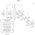
Fig. 1 is a side view illustrating a configuration of an optical computing device in accordance with an embodiment of the present invention. -
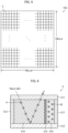
Fig. 2 is a plan view illustrating a specific example of an optical modulation element included in the optical computing device illustrated inFig. 1 . -
Fig. 3 is a partial enlarged perspective view illustrating the optical modulation element illustrated inFig. 2 . -
Fig. 4 is a side view illustrating a variation of the optical computing device illustrated inFig. 1 . -
Fig. 5 is a plan view illustrating a specific example of an optical modulation element included in the optical computing device illustrated inFig. 4 . -
Fig. 6 is a cross-sectional view of a cell included in the optical modulation element illustrated inFig. 5 . - With reference to
Fig. 1 , the following will describe anoptical computing device 1 in accordance with an embodiment of the present invention.Fig. 1 is a side view illustrating a configuration of theoptical computing device 1. - As illustrated in
Fig. 1 , theoptical computing device 1 includes aspatial light modulator 11, alens 12, an opticalmodulation element group 13, and adriver 14. - The
spatial light modulator 11 is a configuration for obtaining signal light L1 indicative of a wave number space image I1, by binary modulation of carrier light L0 for each cell. In the present embodiment, thespatial light modulator 11 is a spatial light modulator that carries out, for each cell, binary intensity modulation or binary phase modulation of the carrier light L0. A spatial light modulator that carries out, for each cell, binary intensity modulation of the carrier light L0 can be, for example, a digital mirror device (DMD). A spatial light modulator that carries out, for each cell, binary phase modulation of the carrier light L0 can be, for example, a ferroelectric liquid crystal on silicon (FLCOS). - The
lens 12 is a configuration for carrying out a Fourier transform of the signal light L1 indicative of the wave number space image I1, to thereby obtain signal light L2 indicative of a real space image I2. In the present embodiment, thelens 12 is a lens having a positive focal length f. Thelens 12 is provided such that: a principal plane of thelens 12 is parallel to an exit surface of thespatial light modulator 11; and a distance between the principal plane of thelens 12 and the exit surface of thespatial light modulator 11 coincides with the focal length f of thelens 12. Examples of a lens having a positive focal length f include a convex lens and a Fresnel lens. Further, a transmissive optical modulation element designed to function as a convex lens can be used as thelens 12. - The optical
modulation element group 13 is a group of n optical modulation elements 13a1 to 13an that sequentially act on the signal light L2. Here, n is any natural number of not less than 1. The example shown inFig. 1 is a case where n = 4. Each of the optical modulation elements 13ai is an element that has an optical computing function, that is, a function of converting a two-dimensional intensity distribution or a two-dimensional phase distribution of signal light in accordance with a predetermined conversion rule. Here, i is a natural number of not less than 1 and not more than n. The opticalmodulation element group 13 is provided such that: an entrance surface of each of the optical modulation elements 13ai is parallel to the principal plane of thelens 12; and a distance between an entrance surface of the optical modulation element 13a1, which is closest to thelens 12, and the principal plane of thelens 12 coincides with the focal length f of thelens 12. In the present embodiment, each of the optical modulation elements 13ai is a transmissive optical modulation element. A specific example of the optical modulation element 13ai will be described later. - To the optical
modulation element group 13, the signal light L2 indicative of the real space image I2 is inputted. The signal light L2 passes through a first optical modulation element 13a1, a second optical modulation element 13a2, ... , and an n-th optical modulation element 13an in this order. Thus, in the opticalmodulation element group 13, computing f = fn·, ... , ·f2·f1 carried out by synthesizing computing f1 by the first optical modulation element 13a1, computing f2 by the second optical modulation element 13a2, ... , and computing fn by the n-th optical modulation element 13an is performed with respect to the real space image I2 indicated by the signal light L2. As such, the opticalmodulation element group 13 makes it possible to obtain signal light L3 that is obtained by applying the computing f to the real space image I2 and that is indicative of an image I3 = f(I2). - The
driver 14 is a configuration for driving the spatiallight modulator 11. Thedriver 14 includes an inverseFourier transform section 14a and abinarizing section 14b. The inverseFourier transform section 14a carries out an inverse Fourier transform of an input image I0 to obtain a wave number space image I1'. The number of gradations of the wave number space image I1' is the same as that of the input image I0, and is, for example, 256. Thebinarizing section 14b binarizes the wave number space image I1' to obtain a binarized wave number space image I1. Thedriver 14 drives the spatiallight modulator 11 so as to generate the signal light L1 indicative of the binarized wave number space image I1. - Note that the
lens 12 can be omitted. In this case, the signal light L1 indicative of the wave number space image I1 is inputted into the opticalmodulation element group 13. In this case, in the opticalmodulation element group 13, computing f = fn·fn-1·, ... , f2·f1 carried out by synthesizing computing f1 by the first optical modulation element 13a1, computing f2 by the second optical modulation element 13a2, ... , computing fn-1 by an n-1-th optical modulation element 13an-1, and computing fn by the n-th optical modulation element 13an is performed with respect to the wave number space image I1 indicated by the signal light L1. As such, the opticalmodulation element group 13 makes it possible to obtain signal light L3 that is obtained by applying the computing f to the wave number space image I1 and that is indicative of an image I3 = f(I1). - Further, the
optical computing device 1 can include a light source that generates the carrier light L0, in addition to the configurations described above. Further, theoptical computing device 1 can include, in addition to the configurations described above, a two-dimensional image sensor that converts the signal light L3 indicative of the image I3 into an electrical signal indicative of the image I3. - Further, the distance between the exit surface of the spatial
light modulator 11 and the principal plane of thelens 12 does not have to exactly coincide with the focal length f of thelens 12. Likewise, the distance between the principal plane of thelens 12 and the entrance surface of the optical modulation element 13a1 does not have to exactly coincide with the focal length f of thelens 12. Even in a case where these distances do not exactly coincide with the focal length f of thelens 12, the signal light L2 entering the opticalmodulation element group 13 includes components indicative of the real space image I2. As such, it is possible to carry out optical computing equivalent to optical computing in a case where these distances exactly coincide with the focal length f of thelens 12. - The optical modulation elements 13a1 to 13an may be integrated together. For example, n light diffraction layers formed inside a structure that allows signal light to pass therethrough, such as a dried gel may be used as the optical modulation elements 13a1 to 13an. In this case, it is preferable to use a gel that is subjected to dehydration shrinkage so that the gel shrinks while keeping a similar shape, e.g., a gel used in the Implosion Fabrication process. This makes it possible to, by drying a swollen gel in which n light diffraction layers are formed, easily manufacture the optical
modulation element group 13 in which the optical modulation elements 13a1 to 13an are arranged with high precision. - The following description will discuss, with reference to
Figs. 2 and 3 , a specific example of the transmissive optical modulation element 13ai.Fig. 2 is a plan view of the optical modulation element 13ai in accordance with the present specific example.Fig. 3 is an enlarged perspective view of a part (i.e., a part surrounded by the broken lines inFig. 2 ) of the optical modulation element 13ai in accordance with the present specific example. - As shown in
Fig. 2 , the optical modulation element 13ai is constituted by a plurality of microcells C having respective phase-modulation amounts that are set independently of each other. When signal light enters the optical modulation element 13ai, the signal light is phase-modulated by the microcells C, and signal light beams thus phase-modulated by the microcells C interfere with each other. Consequently, predetermined optical computing (conversion of a two-dimensional intensity distribution according to a predetermined conversion rule) is carried out. The phase modulation amounts of the microcells C may be variable or may be fixed. In the present specific example, the phase modulation amounts are fixed. - In the present specification, "microcell" means a cell having a cell size of less than 10 pm, for example. Further, "cell size" means a square root of an area of a cell. For example, given that the microcell C is in the form of a square in a plan view, a cell size of the microcell C means a length of one side of the microcell C. A lower limit of the cell size of the microcell C is 1 nm, for example.
- The optical modulation element 13ai shown in
Fig. 2 as an example is constituted by 200 × 200 microcells C arranged in matrix. A shape of each microcell C in a plan view is a square of 500 nm × 500 nm. A shape of the optical modulation element 13ai in a plan view is a square of 100 pm × 100 pm. - A phase-modulation amount of signal light that passes through each microcell C can be set independently for the cell by (1) setting a thickness of the microcell C independently for the cell or (2) selecting a refractive index of the microcell C independently for the cell. The present embodiment employs the method (1), which can be carried out by nanoimprinting. In this case, as shown in
Fig. 3 , each microcell C is constituted by a pillar having a quadrangular prism shape having a square bottom surface with sides each having a length equal to a cell size. In this case, the phase-modulation amount of the signal light passing through each microcell C is determined in accordance with a height of a pillar constituting the microcell C. That is, signal light that passes through a microcell C constituted by a pillar having a high height has a large phase-modulation amount, whereas signal light that passes through a microcell C constituted by a pillar having a low height has a small phase-modulation amount. - Note that the phase-modulation amount of each of the microcells C can be set, for example, through machine learning. A model used in this machine learning can be, for example, a model in which a two-dimensional intensity distribution of signal light inputted into the optical modulation element 13ai is an input, and a two-dimensional intensity distribution of signal light outputted from the optical modulation element 13ai is an output and which includes a phase-modulation amount of each of the microcells C as a parameter. Here, the two-dimensional intensity distribution of the signal light inputted into the optical modulation element 13ai means a set of intensities of signal light beams inputted into the respective microcells that constitute the optical modulation element 13ai. Further, the two-dimensional intensity distribution of the signal light outputted from the optical modulation element 13ai means: a set of intensities of signal light beams inputted into respective microcells C that constitute an optical
modulation element 13ai+ 1 disposed to follow the optical modulation element 13ai; or a set of intensities of signal light beams inputted into respective microcells that constitute a two-dimensional image sensor disposed to follow the optical modulation element 13ai. - In the
optical computing device 1, the opticalmodulation element group 13 is constituted by transmissive optical modulation elements 13a1 to 13an. The present invention, however, is not limited to this. That is, the opticalmodulation element group 13 can be constituted by reflective optical modulation elements 13b1 to 13bn. -
Fig. 4 is a side view illustrating a configuration of an optical computing device 1A in which an opticalmodulation element group 13 is constituted by reflective optical modulation elements 13b1 to 13bn. In the optical computing device 1A, signal light L3 is obtained by causing signal light L2 to be (1) modulated and reflected by the optical modulation element 13b1, (2) modulated and reflected by an optical modulation element 13b2, (3) modulated and reflected by an optical modulation element 13b3, and (4) modulated and reflected by an optical modulation element 13b4. - In the optical computing device 1A, the optical modulation element 13b1 is provided such that a center of the optical modulation element 13b1 is located at a focal point of a
lens 12. As such, in the optical computing device 1A, a signal light beam L2 that enters the center of the optical modulation element 13b1 has an intensity equal to an intensity of a signal light beam L2 that enters a center of the optical modulation element 13a1 of theoptical computing device 1. Meanwhile, in the optical computing device 1A, a main surface of the optical modulation element 13b1 is not orthogonal to an optical axis of thelens 12. As such, in the optical computing device 1A, a signal light beam L2 that enters a point in the optical modulation element 13b1 other than the center of the optical modulation element 13b1 has an intensity not equal to an intensity of a signal light beam L2 that enters a corresponding point in the optical modulation element 13a of theoptical computing device 1. Thus, an intensity distribution of the signal light L2 entering the optical modulation element 13b1 indicates an approximate real space image I2', rather than an exact real space image I2. As such, respective phase-modulation amounts of the cells constituting each of the optical modulation elements 13b1 to 13bn are designed such that desired optical computing is carried out when the approximate real space image I2' enters the optical modulation element 13b1. - The optical modulation elements 13b1 and 13b3, which are provided on the same plane, may be integrated together. For example, the optical modulation elements 13b1 and 13b3 can be embedded in a single substrate, or two regions of a single optical modulation element can be used as the optical modulation elements 13b1 and 13b3. The same is true of the optical modulation elements 13b2 and 13b4 which are provided on the same plane. Further, four light diffraction layers formed inside a structure that allows signal light to pass therethrough, such as a dried gel may be used as the optical modulation elements 13b1 to 13b4. In this case, it is preferable to use a gel that is subjected to dehydration shrinkage so that the gel shrinks while keeping a similar shape, e.g., a gel used in the Implosion Fabrication process. This makes it possible to, by drying a swollen gel in which four light diffraction layers are formed, easily manufacture the optical
modulation element group 13 in which the optical modulation elements 13b1 to 13b4 are arranged with high precision. - The following description will discuss, with reference to
Figs. 5 and 6 , a specific example of a reflective optical modulation element 13bi.Fig. 5 is a plan view of the optical modulation element 13bi in accordance with the present specific example.Fig. 6 is a cross-sectional view of a microcell C included in the optical modulation element 13bi in accordance with the present specific example. - As shown in
Fig. 5 , the optical modulation element 13bi includes a plurality of microcells C having respective phase-modulation amounts that can be set independently of each other. When signal light enters the optical modulation element 13bi, the signal light is phase-modulated by the microcells C, and signal light beams thus phase-modulated by the microcells C interfere with each other. Consequently, predetermined optical computing (conversion of a two-dimensional intensity distribution according to a predetermined conversion rule) is carried out. The phase-modulation amounts of the microcells C may be variable or may be fixed. In the present specific example, the phase-modulation amounts are variable. - The optical modulation element 13bi shown in
Fig. 5 as an example is constituted by 200 × 200 microcells C arranged in matrix. A shape of each microcell C in a plan view is a square of 500 nm × 500 nm. A shape of the optical modulation element 13bi in a plan view is a square of 100 pm × 100 pm. - For example, as shown in
Fig. 6 , each microcell C included in the optical modulation element 13bi may include a polarizing plate C11, a reflecting plate C12, a first electrode C13, a magnetization free layer C14, an insulating layer C15, a magnetization fixed layer C16, and a second electrode C17. - The polarizing plate C11 and the reflecting plate C12 are disposed opposite to each other. The first electrode C13, the magnetization free layer C14, the insulating layer C15, the magnetization fixed layer C16, and the second electrode C17 are stacked in this order, and are sandwiched between the polarizing plate C11 and the reflecting plate C12. Here, a direction in which the first electrode C13, the magnetization free layer C14, the insulating layer C15, the magnetization fixed layer C16, and the second electrode C17 are stacked is orthogonal to a direction in which the polarizing plate C11 and the reflecting plate C12 are stacked. Thus, a first side surface of the magnetization free layer C14 is in surface contact with one of main surfaces of the first polarizing plate C11, and a second side surface of the magnetization free layer C14 which is located opposite to the first side surface is in surface contact with one of main surfaces of the reflecting plate C12. The signal light L (1) enters an inside of the magnetization free layer C14 via the polarizing plate C11, (2) is reflected by the reflecting plate C12, and (3) is emitted through the polarizing plate C11 to an outside of the magnetization free layer C14.
- The magnetization free layer C14 is made of, for example, a soft magnetic material having electric conductivity and light transmissivity (for example, CoFeB). The magnetization fixed layer C16 is made of, for example, a hard magnetic material having electric conductivity (for example, permalloy). Selected as the polarizing plate C11 is a polarizing plate that selectively allows, to pass therethrough, a polarized light component having a polarization direction P parallel to a magnetization direction M of the magnetization fixed layer C16.
Fig. 6 takes as an example a case in which the magnetization direction M and the polarization direction P are parallel to both (i) the main surfaces of the polarizing plate C11 and (ii) main surfaces of the magnetization fixed layer C 16. - When a potential difference is provided between the first electrode C13 and the second electrode C17, a tunnel effect occurs and injects a spin current (a flow of spin-polarized electrons) from the magnetization fixed layer C16 through the insulating layer C15 into the magnetization free layer C14 to magnetize the magnetization free layer C14. Here, the magnetization occurring in the magnetization free layer C14 is magnetization parallel to the magnetization direction M of the magnetization fixed layer C16, that is, magnetization parallel to the polarization direction P of the signal light entering the magnetization free layer C14 through the polarizing plate C11. This causes a phase of the signal light to be delayed by a transverse Kerr effect during a process of transmission in the magnetization free layer C14.
- Here, a phase-shift amount of the signal light in the cell C is determined depending on a magnitude of the magnetization in the magnetization free layer C14. The magnitude of the magnetization in the magnetization free layer C14 is determined depending on a magnitude of the spin current injected into the magnetization free layer C14. The magnitude of the spin current injected into the magnetization free layer C14 is determined depending on the potential difference provided between the first electrode C13 and the second electrode C17. Thus, regulating the potential difference provided between the first electrode C13 and the second electrode C17 can regulate phase modulating of the cell C.
- Note that the phase-modulation amount of each of the microcells C can be set, for example, through machine learning. A model used in this machine learning can be, for example, a model in which a two-dimensional intensity distribution of signal light inputted into the optical modulation element 13bi is an input, and a two-dimensional intensity distribution of signal light outputted from the optical modulation element 13bi is an output and which includes a phase-modulation amount of each of the microcells C as a parameter. Here, the two-dimensional intensity distribution of the signal light inputted into the optical modulation element 13bi means a set of intensities of signal light beams inputted into the respective microcells that constitute the optical modulation element 13bi. Further, the two-dimensional intensity distribution of the signal light outputted from the optical modulation element 13bi means: a set of intensities of signal light beams inputted into respective microcells C that constitute an optical modulation element 13bi+1 disposed to follow the optical modulation element 13bi; or a set of intensities of signal light beams inputted into respective microcells that constitute a two-dimensional image sensor disposed to follow the optical modulation element 13bi.
- An optical computing device in accordance with
Aspect 1 of the present invention is an optical computing device, including: a spatial light modulator that carries out, for each cell, binary modulation of carrier light to thereby generate signal light indicative of a wave number space image; and an optical modulation element group consisting of at least one optical modulation element that sequentially acts on the signal light. - According to the above configuration, the spatial light modulator that carries out, for each cell, binary modulation of carrier light is used. This makes it possible to carry out high-speed optical computing. Further, according to the above configuration, the spatial light modulator generates signal light indicative of a wave number space image. As such, an image to be supplied to the spatial light modulator can be generated by binarization of a wave number space image. This allows information loss from binarization to be reduced as compared with a case in which an image to be supplied to a modulator is generated by binarization of a real space image. As such, according to the above configuration, it is possible to carry out high-speed optical computing while reducing information loss from binarization.
- An optical computing device in accordance with
Aspect 2 of the present invention employs, in addition to the configuration in accordance withAspect 1, a configuration in which the optical computing device further includes a lens that carries out a Fourier transform of the signal light, wherein the optical modulation element group acts on signal light obtained by the lens and indicative of a real space image. - According to the above configuration, it is possible to carry out high-speed optical computing with respect to signal light indicative of a real space image, while reducing information loss from binarization.
- An optical computing device in accordance with Aspect 3 of the present invention employs, in addition to the configuration in accordance with
Aspect 2, a configuration in which: the lens is a lens having a positive focal length; and a distance between an exit surface of the spatial light modulator and a principal plane of the lens and a distance between the principal plane of the lens and an entrance surface of an optical modulation element closest to the lens each coincide with a focal length of the lens. - According to the above configuration, it is possible to carry out a Fourier transform of signal light with use of a simple configuration.
- An optical computing device in accordance with Aspect 4 of the present invention employs, in addition to the configuration in accordance with any one of
Aspects 1 to 3, a configuration in which the optical computing device further includes a driver that drives the spatial light modulator and includes (i) an inverse Fourier transform section that carries out an inverse Fourier transform of an input image to thereby generate a wave number space image and (ii) a binarizing section that binarizes the wave number space image to thereby generate the wave number space image. - According to the above configuration, it is possible to, while reducing information loss from binarization, carry out high-speed optical computing with respect to signal light indicative of: a wave number space image (in a case where the optical computing device does not include a lens) obtained by carrying out an inverse Fourier transform of an input image; or a real space image (in a case where the optical computing device includes a lens) obtained by carrying out a Fourier transform of the wave number space image.
- An optical computing device in accordance with Aspect 5 of the present invention employs, in addition to the configuration of any one of
Aspects 1 to 4, a configuration in which the spatial light modulator is a digital mirror device (DMD) or a ferroelectric liquid crystal on silicon (FLCOS). - According to the above configuration, it is possible to carry out binary modulation for each cell with use of a simple configuration.
- An optical computing device in accordance with Aspect 6 of the present invention employs, in addition to the configuration in accordance with any one of
Aspects 1 to 5, a configuration in which each optical modulation element included in the optical modulation element group is constituted by a plurality of microcells having respective phase-modulation amounts that are settable independently of each other. - According to the above configuration, it is possible to carry out optical computing with respect to signal light with use of a simple configuration.
- An optical computing device in accordance with Aspect 7 of the present invention employs, in addition to the configuration in accordance with any one of
Aspects 1 to 6, a configuration in which each optical modulation element included in the optical modulation element group is a transmissive optical modulation element. - According to the above configuration, it is possible to input, into the optical modulation element group, signal light that indicates a real space image more accurately, as compared with a case in which an optical modulation element is constituted by a reflective optical modulation element.
- An optical computing method in accordance with Aspect 8 of the present invention is an optical computing method, including the steps of: carrying out, for each cell, binary modulation of carrier light to thereby generate signal light indicative of a wave number space image; and carrying out optical computing by causing at least one optical modulation element to sequentially act on the signal light.
- According to the above configuration, it is possible to carry out high-speed optical computing while reducing information loss from binarization.
- An optical computing device in accordance with
Aspect 1 of the present invention is an optical computing device, including: a spatial light modulator that carries out, for each cell, binary modulation of carrier light to thereby generate signal light indicative of a wave number space image; and an optical modulation element group consisting of at least one optical modulation element that sequentially acts on the signal light. - According to the above configuration, the spatial light modulator that carries out, for each cell, binary modulation of carrier light is used. This makes it possible to carry out high-speed optical computing. Further, according to the above configuration, the spatial light modulator generates signal light indicative of a wave number space image. As such, an image to be supplied to the spatial light modulator can be generated by binarization of a wave number space image. This allows information loss from binarization to be reduced as compared with a case in which an image to be supplied to a modulator is generated by binarization of a real space image. As such, according to the above configuration, it is possible to carry out high-speed optical computing while reducing information loss from binarization.
- An optical computing device in accordance with
Aspect 2 of the present invention employs, in addition to the configuration in accordance withAspect 1, a configuration in which the optical computing device further includes a lens that carries out a Fourier transform of the signal light, wherein the optical modulation element group acts on signal light obtained by the lens and indicative of a real space image. - According to the above configuration, it is possible to carry out high-speed optical computing with respect to signal light indicative of a real space image, while reducing information loss from binarization.
- An optical computing device in accordance with Aspect 3 of the present invention employs, in addition to the configuration in accordance with
Aspect 2, a configuration in which: the lens is a lens having a positive focal length; and a distance between an exit surface of the spatial light modulator and a principal plane of the lens and a distance between the principal plane of the lens and an entrance surface of an optical modulation element closest to the lens each coincide with a focal length of the lens. - According to the above configuration, it is possible to carry out a Fourier transform of signal light with use of a simple configuration.
- An optical computing device in accordance with Aspect 4 of the present invention employs, in addition to the configuration in accordance with any one of
Aspects 1 to 3, a configuration in which the optical computing device further includes a driver that drives the spatial light modulator and includes (i) an inverse Fourier transform section that carries out an inverse Fourier transform of an input image to thereby generate a wave number space image and (ii) a binarizing section that binarizes the wave number space image to thereby generate the wave number space image. - According to the above configuration, it is possible to, while reducing information loss from binarization, carry out high-speed optical computing with respect to signal light indicative of: a wave number space image (in a case where the optical computing device does not include a lens) obtained by carrying out an inverse Fourier transform of an input image; or a real space image (in a case where the optical computing device includes a lens) obtained by carrying out a Fourier transform of the wave number space image.
- An optical computing device in accordance with Aspect 5 of the present invention employs, in addition to the configuration of any one of
Aspects 1 to 4, a configuration in which the spatial light modulator is a digital mirror device (DMD) or a ferroelectric liquid crystal on silicon (FLCOS). - According to the above configuration, it is possible to carry out binary modulation for each cell with use of a simple configuration.
- An optical computing device in accordance with Aspect 6 of the present invention employs, in addition to the configuration in accordance with any one of
Aspects 1 to 5, a configuration in which each optical modulation element included in the optical modulation element group is a reflective optical modulation element and is constituted by a plurality of microcells having respective phase-modulation amounts that are settable independently of each other. - According to the above configuration, it is possible to carry out optical computing with respect to signal light with use of a simple configuration.
- An optical computing device in accordance with Aspect 7 of the present invention employs, in addition to the configuration in accordance with any one of
Aspects 1 to 5, a configuration in which each optical modulation element included in the optical modulation element group is a transmissive optical modulation element and is constituted by a plurality of microcells having respective phase-modulation amounts that are set independently of each other. - According to the above configuration, it is possible to input, into the optical modulation element group, signal light that indicates a real space image more accurately, as compared with a case in which an optical modulation element is constituted by a reflective optical modulation element.
- An optical computing method in accordance with Aspect 8 of the present invention is an optical computing method, including the steps of: carrying out, for each cell, binary modulation of carrier light to thereby generate signal light indicative of a wave number space image; and carrying out optical computing by causing at least one optical modulation element to sequentially act on the signal light.
- According to the above configuration, it is possible to carry out high-speed optical computing while reducing information loss from binarization.
- The present invention is not limited to the description of the embodiments, but can be altered in many ways by a person skilled in the art within the scope of the claims. An embodiment derived from a proper combination of technical means disclosed in different embodiments is also encompassed in the technical scope of the present invention.
-
- 1: Optical computing device
- 11: Spatial light modulator
- 12: Lens
- 13: Optical modulation element group
- 13a1 to 13an: Optical modulation element
Claims (8)
- An optical computing device, comprising: a spatial light modulator that carries out, for each cell, binary modulation of carrier light to thereby generate signal light indicative of a wave number space image; and
an optical modulation element group consisting of at least one optical modulation element that sequentially acts on the signal light. - The optical computing device as set forth in claim 1, further comprising:a lens that carries out a Fourier transform of the signal light,wherein the optical modulation element group acts on signal light obtained by the lens and indicative of a real space image.
- The optical computing device as set forth in claim 2, wherein:the lens is a lens having a positive focal length; anda distance between an exit surface of the spatial light modulator and a principal plane of the lens and a distance between the principal plane of the lens and an entrance surface of an optical modulation element closest to the lens each coincide with a focal length of the lens.
- The optical computing device as set forth in any one of claims 1 to 3, further comprising:
a driver that drives the spatial light modulator and includes (i) an inverse Fourier transform section that carries out an inverse Fourier transform of an input image to thereby generate a wave number space image and (ii) a binarizing section that binarizes the wave number space image to thereby generate the wave number space image. - The optical computing device as set forth in any one of claims 1 to 4, wherein the spatial light modulator is a digital mirror device (DMD) or a ferroelectric liquid crystal on silicon (FLCOS) .
- The optical computing device as set forth in any one of claims 1 to 5, wherein each optical modulation element included in the optical modulation element group is a reflective optical modulation element and is constituted by a plurality of microcells having respective phase-modulation amounts that are settable independently of each other.
- The optical computing device as set forth in any one of claims 1 to 6, wherein each optical modulation element included in the optical modulation element group is a transmissive optical modulation element and is constituted by a plurality of microcells having respective phase-modulation amounts that are set independently of each other.
- An optical computing method, comprising the steps of: carrying out, for each cell, binary modulation of carrier light to thereby generate signal light indicative of a wave number space image; and
carrying out optical computing by causing at least one optical modulation element to sequentially act on the signal light.
Applications Claiming Priority (2)
| Application Number | Priority Date | Filing Date | Title |
|---|---|---|---|
| JP2022007193 | 2022-01-20 | ||
| PCT/JP2022/043478 WO2023139922A1 (en) | 2022-01-20 | 2022-11-25 | Optical computation device and optical computation method |
Publications (2)
| Publication Number | Publication Date |
|---|---|
| EP4468075A1 true EP4468075A1 (en) | 2024-11-27 |
| EP4468075A4 EP4468075A4 (en) | 2026-01-07 |
Family
ID=87348036
Family Applications (1)
| Application Number | Title | Priority Date | Filing Date |
|---|---|---|---|
| EP22922073.6A Pending EP4468075A4 (en) | 2022-01-20 | 2022-11-25 | OPTICAL CALCULATION DEVICE AND OPTICAL CALCULATION METHOD |
Country Status (5)
| Country | Link |
|---|---|
| US (1) | US20250130610A1 (en) |
| EP (1) | EP4468075A4 (en) |
| JP (1) | JP7745655B2 (en) |
| CN (1) | CN118541638A (en) |
| WO (1) | WO2023139922A1 (en) |
Family Cites Families (8)
| Publication number | Priority date | Publication date | Assignee | Title |
|---|---|---|---|---|
| US4978950A (en) * | 1989-07-14 | 1990-12-18 | The Boeing Company | Grey-scale representation using binary spatial light modulators in coherent optical processor |
| JP2749944B2 (en) * | 1990-04-03 | 1998-05-13 | 三菱重工業株式会社 | Optical arithmetic unit |
| JP2837975B2 (en) * | 1991-07-16 | 1998-12-16 | 松下電器産業株式会社 | Spatial light modulator and optical operation device |
| DE69816876T2 (en) * | 1998-09-24 | 2004-04-22 | Qinetiq Ltd. | IMPROVEMENTS REGARDING PATTERN RECOGNITION |
| GB0704773D0 (en) * | 2007-03-13 | 2007-04-18 | Cambridge Correlators Ltd | Optical derivative and mathematical operator processor |
| US7847225B2 (en) | 2008-05-02 | 2010-12-07 | Hiroshima University | Optical neural network |
| GB2461894B (en) * | 2008-07-16 | 2010-06-23 | Light Blue Optics Ltd | Holographic image display systems |
| US11170318B2 (en) * | 2019-10-31 | 2021-11-09 | Nxgen Partners Ip, Llc | Multi-photon, multi-dimensional hyper-entanglement using higher-order radix qudits with applications to quantum computing, QKD and quantum teleportation |
-
2022
- 2022-11-25 EP EP22922073.6A patent/EP4468075A4/en active Pending
- 2022-11-25 WO PCT/JP2022/043478 patent/WO2023139922A1/en not_active Ceased
- 2022-11-25 US US18/730,432 patent/US20250130610A1/en active Pending
- 2022-11-25 CN CN202280088247.6A patent/CN118541638A/en active Pending
- 2022-11-25 JP JP2023575093A patent/JP7745655B2/en active Active
Also Published As
| Publication number | Publication date |
|---|---|
| CN118541638A (en) | 2024-08-23 |
| WO2023139922A1 (en) | 2023-07-27 |
| EP4468075A4 (en) | 2026-01-07 |
| JP7745655B2 (en) | 2025-09-29 |
| JPWO2023139922A1 (en) | 2023-07-27 |
| US20250130610A1 (en) | 2025-04-24 |
Similar Documents
| Publication | Publication Date | Title |
|---|---|---|
| CN112749808B (en) | Addressing control system and addressing control method | |
| Marrakchi et al. | Physical characterization of the photorefractive incoherent-to-coherent optical converter | |
| Song et al. | Printing polarization and phase at the optical diffraction limit: near-and far-field optical encryption | |
| Tanuwijaya et al. | Metasurface for programmable quantum algorithms with classical and quantum light | |
| Mehta | Integrated optical quantum manipulation and measurement of trapped ions | |
| Dan et al. | Optoelectronic integrated circuits for analog optical computing: Development and challenge | |
| US20100039686A1 (en) | Hologram pattern generation method and multiple light points generation apparatus | |
| Zhang et al. | Space‐time projection enabled ultrafast all‐optical diffractive neural network | |
| EP4468075A1 (en) | Optical computation device and optical computation method | |
| Shen et al. | Electrically tunable all-dielectric metasurfaces integrated with nematic liquid crystals for information encryption | |
| Wang et al. | Innovative OPA-based optical chip for enhanced digital holography | |
| CN113589560A (en) | Method and system for generating orbital angular momentum optical comb based on angular binarization phase | |
| Bazhenov et al. | Optical Processing | |
| Yang et al. | Generation of optical vortex beams | |
| CN114675467B (en) | An improved quasi-multi-valued coding method for nonlinear light field control | |
| Tooley et al. | Optical computing | |
| Gao et al. | Relief-surface-based on-chip hybrid diffraction neural network enabled by authentic all-optical fully connected architecture | |
| Gulkin et al. | Ultrafast Diffraction Shaping by Periodic Arrays of GaAs Nanoantennas | |
| EP4564089A1 (en) | Optical computation device | |
| US6023353A (en) | Method of designing a spatial phase modulation element and a spatial phase modulation element | |
| EP4481486A1 (en) | Optical switch and switching method | |
| EP4383141A1 (en) | Fast optical qubit addressing | |
| Yang et al. | A metasurface processor that supports synchronous operation of analog and digital computing | |
| Ramesh et al. | A spatial-photonic Ising machine to solve the two-way number-partitioning problem | |
| Kazanskiy et al. | Optical Computing: Key Problems, Achievements, and Perspectives |
Legal Events
| Date | Code | Title | Description |
|---|---|---|---|
| STAA | Information on the status of an ep patent application or granted ep patent |
Free format text: STATUS: THE INTERNATIONAL PUBLICATION HAS BEEN MADE |
|
| PUAI | Public reference made under article 153(3) epc to a published international application that has entered the european phase |
Free format text: ORIGINAL CODE: 0009012 |
|
| STAA | Information on the status of an ep patent application or granted ep patent |
Free format text: STATUS: REQUEST FOR EXAMINATION WAS MADE |
|
| 17P | Request for examination filed |
Effective date: 20240716 |
|
| AK | Designated contracting states |
Kind code of ref document: A1 Designated state(s): AL AT BE BG CH CY CZ DE DK EE ES FI FR GB GR HR HU IE IS IT LI LT LU LV MC ME MK MT NL NO PL PT RO RS SE SI SK SM TR |
|
| DAV | Request for validation of the european patent (deleted) | ||
| DAX | Request for extension of the european patent (deleted) | ||
| A4 | Supplementary search report drawn up and despatched |
Effective date: 20251209 |
|
| RIC1 | Information provided on ipc code assigned before grant |
Ipc: G02F 3/00 20060101AFI20251203BHEP Ipc: G06E 3/00 20060101ALI20251203BHEP Ipc: G02B 26/08 20060101ALI20251203BHEP Ipc: G02F 1/13 20060101ALI20251203BHEP Ipc: G02F 1/1335 20060101ALI20251203BHEP Ipc: G02B 26/06 20060101ALI20251203BHEP Ipc: G02F 1/1362 20060101ALI20251203BHEP Ipc: G03H 1/02 20060101ALI20251203BHEP Ipc: G03H 1/22 20060101ALI20251203BHEP Ipc: G03H 1/28 20060101ALI20251203BHEP Ipc: G06N 3/067 20060101ALI20251203BHEP |