EP4468070A1 - Assisted thermo-optic phase shifters - Google Patents
Assisted thermo-optic phase shifters Download PDFInfo
- Publication number
- EP4468070A1 EP4468070A1 EP23209945.7A EP23209945A EP4468070A1 EP 4468070 A1 EP4468070 A1 EP 4468070A1 EP 23209945 A EP23209945 A EP 23209945A EP 4468070 A1 EP4468070 A1 EP 4468070A1
- Authority
- EP
- European Patent Office
- Prior art keywords
- heating element
- resistive heating
- waveguide core
- heater
- ridge
- Prior art date
- Legal status (The legal status is an assumption and is not a legal conclusion. Google has not performed a legal analysis and makes no representation as to the accuracy of the status listed.)
- Pending
Links
Images


Classifications
-
- G—PHYSICS
- G02—OPTICS
- G02F—OPTICAL DEVICES OR ARRANGEMENTS FOR THE CONTROL OF LIGHT BY MODIFICATION OF THE OPTICAL PROPERTIES OF THE MEDIA OF THE ELEMENTS INVOLVED THEREIN; NON-LINEAR OPTICS; FREQUENCY-CHANGING OF LIGHT; OPTICAL LOGIC ELEMENTS; OPTICAL ANALOGUE/DIGITAL CONVERTERS
- G02F1/00—Devices or arrangements for the control of the intensity, colour, phase, polarisation or direction of light arriving from an independent light source, e.g. switching, gating or modulating; Non-linear optics
- G02F1/01—Devices or arrangements for the control of the intensity, colour, phase, polarisation or direction of light arriving from an independent light source, e.g. switching, gating or modulating; Non-linear optics for the control of the intensity, phase, polarisation or colour
- G02F1/0147—Devices or arrangements for the control of the intensity, colour, phase, polarisation or direction of light arriving from an independent light source, e.g. switching, gating or modulating; Non-linear optics for the control of the intensity, phase, polarisation or colour based on thermo-optic effects
-
- G—PHYSICS
- G02—OPTICS
- G02F—OPTICAL DEVICES OR ARRANGEMENTS FOR THE CONTROL OF LIGHT BY MODIFICATION OF THE OPTICAL PROPERTIES OF THE MEDIA OF THE ELEMENTS INVOLVED THEREIN; NON-LINEAR OPTICS; FREQUENCY-CHANGING OF LIGHT; OPTICAL LOGIC ELEMENTS; OPTICAL ANALOGUE/DIGITAL CONVERTERS
- G02F1/00—Devices or arrangements for the control of the intensity, colour, phase, polarisation or direction of light arriving from an independent light source, e.g. switching, gating or modulating; Non-linear optics
- G02F1/01—Devices or arrangements for the control of the intensity, colour, phase, polarisation or direction of light arriving from an independent light source, e.g. switching, gating or modulating; Non-linear optics for the control of the intensity, phase, polarisation or colour
- G02F1/0102—Constructional details, not otherwise provided for in this subclass
-
- G—PHYSICS
- G02—OPTICS
- G02F—OPTICAL DEVICES OR ARRANGEMENTS FOR THE CONTROL OF LIGHT BY MODIFICATION OF THE OPTICAL PROPERTIES OF THE MEDIA OF THE ELEMENTS INVOLVED THEREIN; NON-LINEAR OPTICS; FREQUENCY-CHANGING OF LIGHT; OPTICAL LOGIC ELEMENTS; OPTICAL ANALOGUE/DIGITAL CONVERTERS
- G02F1/00—Devices or arrangements for the control of the intensity, colour, phase, polarisation or direction of light arriving from an independent light source, e.g. switching, gating or modulating; Non-linear optics
- G02F1/01—Devices or arrangements for the control of the intensity, colour, phase, polarisation or direction of light arriving from an independent light source, e.g. switching, gating or modulating; Non-linear optics for the control of the intensity, phase, polarisation or colour
- G02F1/011—Devices or arrangements for the control of the intensity, colour, phase, polarisation or direction of light arriving from an independent light source, e.g. switching, gating or modulating; Non-linear optics for the control of the intensity, phase, polarisation or colour in optical waveguides, not otherwise provided for in this subclass
- G02F1/0113—Glass-based, e.g. silica-based, optical waveguides
-
- G—PHYSICS
- G02—OPTICS
- G02F—OPTICAL DEVICES OR ARRANGEMENTS FOR THE CONTROL OF LIGHT BY MODIFICATION OF THE OPTICAL PROPERTIES OF THE MEDIA OF THE ELEMENTS INVOLVED THEREIN; NON-LINEAR OPTICS; FREQUENCY-CHANGING OF LIGHT; OPTICAL LOGIC ELEMENTS; OPTICAL ANALOGUE/DIGITAL CONVERTERS
- G02F1/00—Devices or arrangements for the control of the intensity, colour, phase, polarisation or direction of light arriving from an independent light source, e.g. switching, gating or modulating; Non-linear optics
- G02F1/01—Devices or arrangements for the control of the intensity, colour, phase, polarisation or direction of light arriving from an independent light source, e.g. switching, gating or modulating; Non-linear optics for the control of the intensity, phase, polarisation or colour
- G02F1/015—Devices or arrangements for the control of the intensity, colour, phase, polarisation or direction of light arriving from an independent light source, e.g. switching, gating or modulating; Non-linear optics for the control of the intensity, phase, polarisation or colour based on semiconductor elements having potential barriers, e.g. having a PN or PIN junction
- G02F1/025—Devices or arrangements for the control of the intensity, colour, phase, polarisation or direction of light arriving from an independent light source, e.g. switching, gating or modulating; Non-linear optics for the control of the intensity, phase, polarisation or colour based on semiconductor elements having potential barriers, e.g. having a PN or PIN junction in an optical waveguide structure
-
- G—PHYSICS
- G02—OPTICS
- G02F—OPTICAL DEVICES OR ARRANGEMENTS FOR THE CONTROL OF LIGHT BY MODIFICATION OF THE OPTICAL PROPERTIES OF THE MEDIA OF THE ELEMENTS INVOLVED THEREIN; NON-LINEAR OPTICS; FREQUENCY-CHANGING OF LIGHT; OPTICAL LOGIC ELEMENTS; OPTICAL ANALOGUE/DIGITAL CONVERTERS
- G02F2203/00—Function characteristic
- G02F2203/50—Phase-only modulation
Definitions
- the disclosure relates to photonics chips and, more specifically, to structures for a thermo-optic phase shifter and methods of forming a thermo-optic phase shifter.
- Photonics chips are used in many applications and systems including, but not limited to, data communication systems and data computation systems.
- a photonics chip includes a photonic integrated circuit comprised of optical components, such as modulators, polarizers, and optical couplers, that are used to manipulate light received from a light source, such as a laser or an optical fiber.
- thermo-optic phase shifter is an optical component can be used in a photonic integrated circuit to modulate the phase of light propagating in a waveguide core. Heat is generated by a heater and transferred from the heater to the waveguide core, which is comprised of a material having a refractive index that varies with temperature. The performance of a thermo-optic phase shifter may be contingent upon the efficient transport of heat from the heater to the waveguide core.
- thermo-optic phase shifter Improved structures for a thermo-optic phase shifter and methods of forming a thermo-optic phase shifter are needed.
- a structure for a thermo-optic phase shifter comprises a semiconductor substrate, and a heater including a first resistive heating element, a second resistive heating element, and a slab layer connecting the first resistive heating element to the second resistive heating element.
- the first resistive heating element and the second resistive heating element have a first thickness
- the slab layer has a second thickness that is less than the first thickness.
- the structure further comprises a waveguide core including a portion that is laterally positioned between the first resistive heating element and the second resistive heating element.
- the slab layer of the heater is disposed between the portion of the waveguide core and the semiconductor substrate.
- the slab layer, the first resistive heating element, and the second resistive heating element may comprise silicon, and the first waveguide core may comprise silicon nitride.
- the heater of the structure may further comprise a ridge disposed on the slab layer between the first resistive heating element and the second resistive heating element.
- the ridge may be positioned beneath the first portion of the first waveguide core.
- the ridge, the slab layer, the first resistive heating element, and the second resistive heating element may comprise silicon, and the first waveguide core may comprise silicon nitride.
- the structure may additionally comprise a dielectric layer over the heater; the first waveguide core may be disposed on the dielectric layer, and the dielectric layer may include a portion between the first portion of the first waveguide core and the ridge of the heater.
- the dielectric layer may comprise a first material, and the slab layer, the ridge, the first resistive heating element, and the second resistive heating element comprise a second material having a higher coefficient of thermal conductivity than the first material.
- the first material may be silicon dioxide.
- the ridge may include a first tapered section and a second tapered section, and the first tapered section and the second tapered section may terminate opposite ends of the ridge; additionally or alternatively, the ridge may be centered beneath the first portion of the first waveguide core; additionally or alternatively the ridge may have a third thickness, and the second thickness of the slab layer may be less than the third thickness.
- the structure may comprise a dielectric layer over the heater, wherein the first waveguide core may be disposed on the dielectric layer, and the dielectric layer may include a first portion between the first portion of the first waveguide core and the slab layer of the heater.
- the dielectric layer may include a second portion between the first portion of the first waveguide core and the first resistive heating element, and the dielectric layer may include a second portion between the first portion of the first waveguide core and the second resistive heating element.
- the dielectric layer may comprise a first material, and the slab layer, the first resistive heating element, and the second resistive heating element may comprise a second material having a higher coefficient of thermal conductivity than the first material.
- the first resistive heating element, and the second resistive heating element may additionally comprise a metal silicide.
- the structure with the above described features may further comprise a second waveguide core connected in parallel to the first waveguide core.
- the first portion of the first waveguide core may define a first delay region
- the first waveguide core may include a second portion
- the structure may further comprise a second waveguide core including a first portion that may define a second delay region and a second portion that may be positioned adjacent to the second portion of the first waveguide core to define a coupling region.
- the first waveguide core may be positioned equidistant from the first resistive heating element and the second resistive heating element.
- the structure may additionally comprise an undercut in the semiconductor substrate beneath the slab layer of the heater and a dielectric layer disposed between the undercut and the heater.
- a method of forming a structure for a thermo-optic phase shifter comprises forming a heater including a first resistive heating element, a second resistive heating element, and a slab layer connecting the first resistive heating element to the second resistive heating element.
- the first resistive heating element and the second resistive heating element have a first thickness
- the slab layer has a second thickness that is less than the first thickness.
- the method further comprises forming a waveguide core including a portion that is laterally positioned between the first resistive heating element and the second resistive heating element.
- the slab layer of the heater is disposed between the portion of the waveguide core and a semiconductor substrate.
- a structure 10 for a thermo-optic phase shifter includes a heater 12 that is disposed on, and over, a dielectric layer 14 and a semiconductor substrate 16 of a photonics chip.
- the dielectric layer 14 may be comprised of a dielectric material, such as silicon dioxide, and the semiconductor substrate 16 may be comprised of a semiconductor material, such as single-crystal silicon.
- the dielectric layer 14 may be a buried oxide layer of a silicon-on-insulator substrate.
- the heater 12 includes a resistive heating element 18, a resistive heating element 20, and a slab layer 22 that extends laterally as a strip from the resistive heating element 18 to the resistive heating element 20.
- a rib or ridge 24 may be disposed on the slab layer 22 at a location between the resistive heating element 18 and the resistive heating element 20.
- the ridge 24 may be positioned equidistantly between the resistive heating element 18 and the resistive heating element 20.
- the slab layer 22 may physically connect the resistive heating element 18 to ridge 24 and the resistive heating element 20 to the ridge 24 such that respective thermal conduction paths are defined.
- the resistive heating elements 18, 20 may have a thickness T1.
- the slab layer 22 may have a thickness T2 that is less than the thickness T1 of the resistive heating elements 18, 20.
- the ridge 24 has a thickness T3 that may be equal or substantially equal to the thickness T1.
- the thickness T2 of the slab layer 22 is less than the thickness T3 of the ridge 24. Due to the thickness differentials, a notch is defined as a recessed space between the resistive heating element 18 and the ridge 24, and another notch is defined as a recessed space between the resistive heating element 20 and the ridge 24.
- the resistive heating element 18, resistive heating element 20, and slab layer 22 may adjoin the underlying dielectric layer 14. In an embodiment, the resistive heating element 18, resistive heating element 20, and slab layer 22 may adjoin the dielectric layer 14 in a directly contacting arrangement. In an embodiment, the resistive heating element 18, resistive heating element 20, and slab layer 22 may be positioned on a planar top surface of the underlying dielectric layer 14.
- the resistive heating element 18 may be truncated at opposite ends 25, the resistive heating element 20 may be truncated at opposite ends 26, and the ridge 24 may be truncated at opposite ends 27.
- the resistive heating elements 18, 20 may have a length L between the respective opposite ends 25, 26.
- the ridge 24 may have a length between its opposite ends 27 that is equal to the length L of the resistive heating elements 18, 20.
- the ridge 24 may have a length between its opposite ends 27 that is greater than the length L of the resistive heating elements 18, 20.
- the ridge 24 may have a length between its opposite ends 27 that is less than the length L of the resistive heating elements 18, 20.
- the slab layer 22 may have a length that is equal to the length of the resistive heating elements 18, 20. In an embodiment, the slab layer 22 may have a width that is equal to the distance between the sidewall 19 of the resistive heating element 18 closest to the ridge 24 and the sidewall 21 of the resistive heating element 20 closest to the ridge 24.
- the resistive heating element 18, resistive heating element 20, slab layer 22, and ridge 24 of the heater 12 may be comprised of a semiconductor material, such as single-crystal silicon.
- the resistive heating element 18, resistive heating element 20, slab layer 22, and ridge 24 may be formed by patterning the semiconductor material (e.g., single-crystal silicon) of a device layer of a silicon-on-insulator substrate with multiple lithography and etching processes.
- the resistive heating element 18 and resistive heating element 20 may be doped with either a p-type dopant or an n-type dopant.
- a dielectric layer 28 is formed on, and over, the heater 12.
- the dielectric layer 28 may be comprised of a dielectric material, such as silicon dioxide, having a refractive index that is less than the refractive index of the material constituting the resistive heating element 18, resistive heating element 20, slab layer 22, and ridge 24.
- the heater 12 may be embedded in the dielectric layer 28, and the dielectric layer 28 may have a thickness greater than a height of the resistive heating element 18, resistive heating element 20, slab layer 22, and ridge 24.
- the dielectric layer 28 includes portions that are disposed in the notch defined over the slab layer 22 between the resistive heating element 18 and the ridge 24 and the notch defined over the slab layer 22 between the resistive heating element 20 and the ridge 24.
- the structure 10 includes a waveguide core 30 that is positioned on, and over, the dielectric layer 28.
- the waveguide core 30 includes a lower surface 32 that is adjacent to the slab layer 22 and ridge 24, an upper surface opposite to the lower surface, and opposite side surfaces 34, 36.
- the resistive heating element 18 is positioned adjacent to the side surface 34 of a portion of the waveguide core 30, and the resistive heating element 20 is positioned adjacent to the opposite side surface 36 of the portion of the waveguide core 30. More specifically, the sidewall 19 of the resistive heating element 18 is positioned adjacent to the side surface 34 of a portion of the waveguide core 30, and the sidewall 21 of the resistive heating element 20 is positioned adjacent to the opposite side surface 36 of the portion of the waveguide core 30.
- the waveguide core 30 may overlap with the ridge 24 such that the lower surface 32 is disposed over a portion of the ridge 24.
- the waveguide core 30 may be symmetrically positioned in a lateral direction between the resistive heating element 18 and the resistive heating element 20 such that the side surfaces 34, 36 are equidistantly spaced from the resistive heating element 18, 20.
- the resistive heating elements 18, 20 may be oriented lengthwise aligned parallel to the adjacent portion of the waveguide core 30.
- the waveguide core 30 may be comprised of a material having a refractive index that is greater than the refractive index of silicon dioxide.
- the waveguide core 30 may be comprised of a dielectric material, such as silicon nitride, silicon oxynitride, or aluminum nitride.
- the waveguide core 30 may be formed by depositing a layer comprised of its constituent dielectric material and patterning the deposited layer with lithography and etching processes.
- a dielectric layer 38 is formed on, and over, the waveguide core 30.
- the dielectric layer 38 may be comprised of a dielectric material, such as silicon dioxide, having a refractive index that is less than the refractive index of the material constituting the waveguide core 30.
- the waveguide core 30 may be embedded in the dielectric layer 38, and the dielectric layer 38 may have a thickness greater than a height of the waveguide core 30.
- Contacts 40 are formed that are physically and electrically connected to the resistive heating element 18, and contacts 42 are formed that are physically and electrically connected to the resistive heating element 20.
- the contacts 40, 42 may be comprised of a metal, such as tungsten, that is formed in openings patterned in the dielectric layers 28, 38.
- the contacts 40 may connect the resistive heating element 18 to a power source 44, which can be operated to supply a current that causes Joule heating of the resistive heating element 18 such that heat is transferred from the resistive heating element 18 to the waveguide core 30.
- the contacts 42 may connect the resistive heating element 20 to the power source 44, which can be operated to supply a current that causes Joule heating of the resistive heating element 20 such that heat is transferred from the resistive heating element 20 to the waveguide core 30.
- the power source 44 is operated to supply a current that causes Joule heating of the resistive heating elements 18, 20.
- Heat generated by the resistive heating elements 18, 20 is transferred to the waveguide core 30 through thermal paths that include the slab layer 22 and the ridge 24.
- the temperature of the waveguide core 30 is elevated by the transferred heat.
- the temperature change experienced by the waveguide core 30 is effective to change the refractive index of its material through the thermo-optic effect and to thereby alter the phase of light propagating in the waveguide core 30.
- the heater 12 enables thermal tuning of the refractive index of the waveguide core 30.
- the slab layer 22 and ridge 24 may increase the tuning efficiency during operation of the thermo-optic phase shifter.
- the slab layer 22 and ridge 24 may be comprised of a material having a significantly higher coefficient of thermal conductivity than the material of the dielectric layers 28, 38.
- the increased efficiency for heat transport may increase the maximum achievable temperature of the waveguide core 30 when transporting heat from the heater 12 to the waveguide core 30 such that the change in the refractive index may be maximized.
- Constructing the waveguide core 30 from a dielectric material, such as silicon nitride may provide a power handling capability that is greater than the power handling capability of other materials, such as silicon.
- the structure 10 may be modified to eliminate the ridge 24.
- the slab layer 22 includes a portion beneath the waveguide core 30, and only the dielectric material of the dielectric layer 28 is disposed between the slab layer 22 and the lower surface 32 of the waveguide core 30.
- the slab layer 22 may increase the tuning efficiency during operation of the thermo-optic phase shifter.
- the ridge 24 of the heater 12 may include tapered sections 46, 48 that terminate at its opposite ends 27.
- the ridge 24 may have a length that is greater than the length L of the resistive heating elements 18, 20 and/or the length of the slab layer 22. As a result, all or a portion of each of the tapered sections 46, 48 may extend past the side edges of the slab layer 22 and/or the ends 25, 26 of the resistive heating elements 18, 20.
- Processing continues to form the dielectric layer 28 and the waveguide core 30 over the heater 12, as well as to perform the remainder of the process flow, as previously described.
- an undercut 49 may be formed that extends as a sealed cavity in the semiconductor substrate 16 beneath all or a portion of the slab layer 22.
- the undercut 49 may be centered beneath the ridge 24. The undercut 49 may improve the efficiency of the thermal tuning provided by the thermo-optic phase shifter.
- each of the resistive heating elements 18, 20 may be comprised of a silicide layer 50.
- the silicide layer may be comprised of a metal silicide, such as nickel silicide, formed by a silicidation process the consumes all or a portion of each of the resistive heating elements 18, 20.
- the ridge 24 may lack silicide.
- a structure 51 for a Mach-Zehnder modulator in which the waveguide core 30 includes an arm or branch 52 and an arm or branch 54 that is positioned adjacent to, and spaced laterally from, the branch 52.
- the structure 51 includes an input to the branches 52, 54 of the waveguide core 30 and an output from the branches 52, 54 of the waveguide core 30.
- the branches 52, 54 of the waveguide core 30 initially diverge away from each other at the input to the optical phase shifter into a divided light path.
- the branch 52 may include a portion aligned with a longitudinal axis 56, and the branch 54 may include a portion aligned with a longitudinal axis 58.
- the branches 52, 54 converge back together and merge into a unified light path at an output from the optical phase shifter.
- the heater 12 of the thermo-optic phase shifter may be associated with the branch 52 of the waveguide core 30 such that the wavelength of the light propagating in the branch 52 can be tuned and shifted in phase relative to the wavelength of the light propagating in the branch 54.
- the resistive heating element 18 may be disposed laterally adjacent to the side surface 34 of the waveguide core 30 in branch 52 and the resistive heating element 20 may be disposed laterally adjacent to the side surface 36 of the waveguide core 30 in branch 52.
- an additional heater may be associated with the branch 54 of the waveguide core 30 such that the wavelength of the light propagating in the branch 54 can also be tuned and shifted in phase.
- the heater 12 may be used to heat the branch 52 of the waveguide core 30 in order to, for example, correct phase error due to manufacturing variations as an adjustment mechanism.
- a wavelength division multiplexing device 60 includes a filter stage 62 and a pair of filter stages 64, 66 that are coupled by linking waveguide cores to the filter stage 62.
- Each of the filter stages 62, 64, 66 includes an open terminal that may be coupled to a terminator 68, which may be an absorber or a grating coupler.
- additional channels may be added to the wavelength division multiplexing device 60 by cascading additional filter stages with the filter stages 62, 64, 66.
- the wavelength division multiplexing device 60 may provide either coarse wavelength-dependent demultiplexing or dense wavelength-dependent demultiplexing.
- the wavelength division multiplexing device 60 is a multiple-channel device that is configured to receive optical signals 70 from a waveguide at an input to the filter stage 62 that includes mixed optical signals of multiple different wavelengths.
- the wavelengths of the optical signals 70 may be different wavelengths within the near infrared portion of the electromagnetic spectrum.
- the wavelength division multiplexing device 60 is configured to receive optical signals 70 with four different wavelengths.
- the filter stages 62, 64, 66 of the wavelength division multiplexing device 60 may split or divide the optical signals 70 according to wavelength.
- the filter stage 62 separates the optical power of the optical signals 70 into optical signals 72, 74 characterized by certain wavelengths (e.g., odd wavelengths) and optical signals 76, 78 characterized by certain wavelengths (e.g., even wavelengths).
- the optical signals 72, 74 are provided by a linking waveguide core from an output of the filter stage 62 to an input to the filter stage 64, and the optical signals 76, 78 are provided by a linking waveguide core from another output of the filter stage 62 to an input to the filter stage 66.
- the filter stage 64 separates the optical signals 72 from the optical signals 74, directs the optical signals 72 to a waveguide core at an output, and directs the optical signals 74 to a waveguide core at a different output.
- the filter stage 66 separates the optical signals 76 from the optical signals 78, directs the optical signals 76 to a waveguide core at an output, and directs the optical signals 78 to a waveguide core at a different output.
- Each of the filter stages 62, 64, 66 of the wavelength division multiplexing device 60 may include a wavelength splitter 80, as best shown in FIG. 11 , that integrates at least one instance of the heater 12 to provide a thermo-optic phase shifter.
- the wavelength splitter 80 includes a waveguide core 82 and a waveguide core 84 that define arms.
- the wavelength splitter 80 includes adjacent sections of the waveguide cores 82, 84 that define a directional coupler 86 and adjacent sections of the waveguide cores 82, 84 that define a directional coupler 88.
- the waveguide core 82 of the wavelength splitter 80 includes a phase delay region 90 joined by a bend to the section of the waveguide core 82 participating in the directional coupler 86 and joined by another bend to the section of the waveguide core 82 participating in the directional coupler 86.
- the waveguide core 84 of the wavelength splitter 80 includes a phase delay region 92 joined by a bend to the section of the waveguide core 84 participating in the directional coupler 86 and joined by another bend to the section of the waveguide core 84 participating in the directional coupler 88.
- the phase delay region 90 have a different length than the phase delay region 92 such that light propagating in the different waveguide cores 82, 84 of the wavelength splitter 80 experiences a phase delay.
- the waveguide core 82 in the phase delay region 90 may be disposed over the resistive heating element 18, resistive heating element 20, slab layer 22, and ridge 24 of the heater 12 to provide the phase delay region 90 with a thermo-optic phase shifter.
- the resistive heating elements 18, 20 may be curved to match the curvature of the phase delay region 90.
- the heater 12 provides the ability to actively adjust the amount of the phase shift experienced by light beyond the passive phase shift provided by the different lengths of the phase delay regions 90, 92.
- the phase delay region 92 may be modified to include a similar thermo-optic phase shifter with a heater that can be operated independently of the heater 12 associated with the phase delay region 90.
- the methods as described above are used in the fabrication of integrated circuit chips.
- the resulting integrated circuit chips can be distributed by the fabricator in raw wafer form (e.g., as a single wafer that has multiple unpackaged chips), as a bare die, or in a packaged form.
- the chip may be integrated with other chips, discrete circuit elements, and/or other signal processing devices as part of either an intermediate product or an end product.
- the end product can be any product that includes integrated circuit chips, such as computer products having a central processor or smartphones.
- references herein to terms modified by language of approximation, such as “about”, “approximately”, and “substantially”, are not to be limited to the precise value specified.
- the language of approximation may correspond to the precision of an instrument used to measure the value and, unless otherwise dependent on the precision of the instrument, may indicate a range of +/- 10% of the stated value(s).
- references herein to terms such as “vertical”, “horizontal”, etc. are made by way of example, and not by way of limitation, to establish a frame of reference.
- the term “horizontal” as used herein is defined as a plane parallel to a conventional plane of a semiconductor substrate, regardless of its actual three-dimensional spatial orientation.
- the terms “vertical” and “normal” refer to a direction in the frame of reference perpendicular to the horizontal, as just defined.
- the term “lateral” refers to a direction in the frame of reference within the horizontal plane.
- a feature “connected” or “coupled” to or with another feature may be directly connected or coupled to or with the other feature or, instead, one or more intervening features may be present.
- a feature may be “directly connected” or “directly coupled” to or with another feature if intervening features are absent.
- a feature may be “indirectly connected” or “indirectly coupled” to or with another feature if at least one intervening feature is present.
- a feature “on” or “contacting” another feature may be directly on or in direct contact with the other feature or, instead, one or more intervening features may be present.
- a feature may be “directly on” or in “direct contact” with another feature if intervening features are absent.
- a feature may be “indirectly on” or in “indirect contact” with another feature if at least one intervening feature is present.
- Different features “overlap” if a feature extends over, and covers a part of, another feature.
Landscapes
- Physics & Mathematics (AREA)
- Nonlinear Science (AREA)
- General Physics & Mathematics (AREA)
- Optics & Photonics (AREA)
- Optical Modulation, Optical Deflection, Nonlinear Optics, Optical Demodulation, Optical Logic Elements (AREA)
- Optical Integrated Circuits (AREA)
Abstract
Structures for a thermo-optic phase shifter and methods of forming a thermo-optic phase shifter. The structure comprises a semiconductor substrate, and a heater including a first resistive heating element, a second resistive heating element, and a slab layer connecting the first resistive heating element to the second resistive heating element. The first resistive heating element and the second resistive heating element have a first thickness, and the slab layer has a second thickness that is less than the first thickness. The structure further comprises a waveguide core including a portion that is laterally positioned between the first resistive heating element and the second resistive heating element. The slab layer of the heater is disposed between the portion of the waveguide core and the semiconductor substrate.
Description
- The disclosure relates to photonics chips and, more specifically, to structures for a thermo-optic phase shifter and methods of forming a thermo-optic phase shifter.
- Photonics chips are used in many applications and systems including, but not limited to, data communication systems and data computation systems. A photonics chip includes a photonic integrated circuit comprised of optical components, such as modulators, polarizers, and optical couplers, that are used to manipulate light received from a light source, such as a laser or an optical fiber.
- A thermo-optic phase shifter is an optical component can be used in a photonic integrated circuit to modulate the phase of light propagating in a waveguide core. Heat is generated by a heater and transferred from the heater to the waveguide core, which is comprised of a material having a refractive index that varies with temperature. The performance of a thermo-optic phase shifter may be contingent upon the efficient transport of heat from the heater to the waveguide core.
- Improved structures for a thermo-optic phase shifter and methods of forming a thermo-optic phase shifter are needed.
- In an embodiment of the invention, a structure for a thermo-optic phase shifter is provided. The structure comprises a semiconductor substrate, and a heater including a first resistive heating element, a second resistive heating element, and a slab layer connecting the first resistive heating element to the second resistive heating element. The first resistive heating element and the second resistive heating element have a first thickness, and the slab layer has a second thickness that is less than the first thickness. The structure further comprises a waveguide core including a portion that is laterally positioned between the first resistive heating element and the second resistive heating element. The slab layer of the heater is disposed between the portion of the waveguide core and the semiconductor substrate.
The slab layer, the first resistive heating element, and the second resistive heating element may comprise silicon, and the first waveguide core may comprise silicon nitride.
According to one variant, the heater of the structure may further comprise a ridge disposed on the slab layer between the first resistive heating element and the second resistive heating element. Optionally, the ridge may be positioned beneath the first portion of the first waveguide core. In addition, the ridge, the slab layer, the first resistive heating element, and the second resistive heating element may comprise silicon, and the first waveguide core may comprise silicon nitride.
Further, the structure may additionally comprise a dielectric layer over the heater; the first waveguide core may be disposed on the dielectric layer, and the dielectric layer may include a portion between the first portion of the first waveguide core and the ridge of the heater. Additionally, the dielectric layer may comprise a first material, and the slab layer, the ridge, the first resistive heating element, and the second resistive heating element comprise a second material having a higher coefficient of thermal conductivity than the first material. For instance, the first material may be silicon dioxide.
Further, the ridge may include a first tapered section and a second tapered section, and the first tapered section and the second tapered section may terminate opposite ends of the ridge; additionally or alternatively, the ridge may be centered beneath the first portion of the first waveguide core; additionally or alternatively the ridge may have a third thickness, and the second thickness of the slab layer may be less than the third thickness.
According to a further variant, the structure may comprise a dielectric layer over the heater, wherein the first waveguide core may be disposed on the dielectric layer, and the dielectric layer may include a first portion between the first portion of the first waveguide core and the slab layer of the heater. Additionally, the dielectric layer may include a second portion between the first portion of the first waveguide core and the first resistive heating element, and the dielectric layer may include a second portion between the first portion of the first waveguide core and the second resistive heating element. The dielectric layer may comprise a first material, and the slab layer, the first resistive heating element, and the second resistive heating element may comprise a second material having a higher coefficient of thermal conductivity than the first material.
For both variants mentioned above, the first resistive heating element, and the second resistive heating element may additionally comprise a metal silicide.
Moreover, the structure with the above described features may further comprise a second waveguide core connected in parallel to the first waveguide core.
Moreover, the first portion of the first waveguide core may define a first delay region, and the first waveguide core may include a second portion, and the structure may further comprise a second waveguide core including a first portion that may define a second delay region and a second portion that may be positioned adjacent to the second portion of the first waveguide core to define a coupling region.
Further, the first waveguide core may be positioned equidistant from the first resistive heating element and the second resistive heating element.
Moreover, the structure may additionally comprise an undercut in the semiconductor substrate beneath the slab layer of the heater and a dielectric layer disposed between the undercut and the heater. - In an embodiment of the invention, a method of forming a structure for a thermo-optic phase shifter is provided. The method comprises forming a heater including a first resistive heating element, a second resistive heating element, and a slab layer connecting the first resistive heating element to the second resistive heating element. The first resistive heating element and the second resistive heating element have a first thickness, and the slab layer has a second thickness that is less than the first thickness. The method further comprises forming a waveguide core including a portion that is laterally positioned between the first resistive heating element and the second resistive heating element. The slab layer of the heater is disposed between the portion of the waveguide core and a semiconductor substrate.
- The accompanying drawings, which are incorporated in and constitute a part of this specification, illustrate various embodiments of the invention and, together with a general description of the invention given above and the detailed description of the embodiments given below, serve to explain the embodiments of the invention. In the drawings, like reference numerals refer to like features in the various views.
-
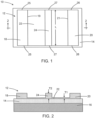
FIG. 1 is a top view of a structure for a thermo-optic phase shifter at an initial fabrication stage of a processing method in accordance with embodiments of the invention. -
FIG. 2 is a cross-sectional view taken generally along line 2-2 inFIG. 1 . -
FIG. 3 is a cross-sectional view of the structure at a fabrication stage of the processing method subsequent toFIGS. 1, 2 . -
FIG. 4 is a cross-sectional view of the structure at a fabrication stage of the processing method subsequent toFIG. 3 . -
FIG. 5 is a cross-sectional view of a structure for a thermo-optic phase shifter in accordance with alternative embodiments of the invention. -
FIG. 6 is a top view of a structure for a thermo-optic phase shifter in accordance with alternative embodiments of the invention. -
FIG. 7 is a cross-sectional view of a structure for a thermo-optic phase shifter in accordance with alternative embodiments of the invention. -
FIG. 8 is a cross-sectional view of a structure for a thermo-optic phase shifter in accordance with alternative embodiments of the invention. -
FIG. 9 is a top view of a structure for a Mach-Zehnder modulator including a thermo-optic phase shifter in accordance with alternative embodiments of the invention. -
FIG. 10 is a diagrammatic top view of a structure for a wavelength division multiplexing device including filter stages in accordance with alternative embodiments of the invention. -
FIG. 11 is a top view of a thermo-optic phase shifter included in a wavelength splitter for the filter stages of the wavelength division multiplexing device ofFIG. 10 . - With reference to
FIGS. 1, 2 and in accordance with embodiments of the invention, astructure 10 for a thermo-optic phase shifter includes aheater 12 that is disposed on, and over, adielectric layer 14 and asemiconductor substrate 16 of a photonics chip. In an embodiment, thedielectric layer 14 may be comprised of a dielectric material, such as silicon dioxide, and thesemiconductor substrate 16 may be comprised of a semiconductor material, such as single-crystal silicon. In an embodiment, thedielectric layer 14 may be a buried oxide layer of a silicon-on-insulator substrate. - The
heater 12 includes aresistive heating element 18, aresistive heating element 20, and aslab layer 22 that extends laterally as a strip from theresistive heating element 18 to theresistive heating element 20. In an embodiment, a rib orridge 24 may be disposed on theslab layer 22 at a location between theresistive heating element 18 and theresistive heating element 20. In an embodiment, theridge 24 may be positioned equidistantly between theresistive heating element 18 and theresistive heating element 20. Theslab layer 22 may physically connect theresistive heating element 18 toridge 24 and theresistive heating element 20 to theridge 24 such that respective thermal conduction paths are defined. - The
resistive heating elements slab layer 22 may have a thickness T2 that is less than the thickness T1 of theresistive heating elements ridge 24 has a thickness T3 that may be equal or substantially equal to the thickness T1. The thickness T2 of theslab layer 22 is less than the thickness T3 of theridge 24. Due to the thickness differentials, a notch is defined as a recessed space between theresistive heating element 18 and theridge 24, and another notch is defined as a recessed space between theresistive heating element 20 and theridge 24. - In an embodiment, the
resistive heating element 18,resistive heating element 20, andslab layer 22 may adjoin the underlyingdielectric layer 14. In an embodiment, theresistive heating element 18,resistive heating element 20, andslab layer 22 may adjoin thedielectric layer 14 in a directly contacting arrangement. In an embodiment, theresistive heating element 18,resistive heating element 20, andslab layer 22 may be positioned on a planar top surface of the underlyingdielectric layer 14. - The
resistive heating element 18 may be truncated at opposite ends 25, theresistive heating element 20 may be truncated at opposite ends 26, and theridge 24 may be truncated at opposite ends 27. Theresistive heating elements ridge 24 may have a length between its opposite ends 27 that is equal to the length L of theresistive heating elements ridge 24 may have a length between its opposite ends 27 that is greater than the length L of theresistive heating elements ridge 24 may have a length between its opposite ends 27 that is less than the length L of theresistive heating elements slab layer 22 may have a length that is equal to the length of theresistive heating elements slab layer 22 may have a width that is equal to the distance between thesidewall 19 of theresistive heating element 18 closest to theridge 24 and thesidewall 21 of theresistive heating element 20 closest to theridge 24. - In an embodiment, the
resistive heating element 18,resistive heating element 20,slab layer 22, andridge 24 of theheater 12 may be comprised of a semiconductor material, such as single-crystal silicon. In an embodiment, theresistive heating element 18,resistive heating element 20,slab layer 22, andridge 24 may be formed by patterning the semiconductor material (e.g., single-crystal silicon) of a device layer of a silicon-on-insulator substrate with multiple lithography and etching processes. In an embodiment, theresistive heating element 18 andresistive heating element 20 may be doped with either a p-type dopant or an n-type dopant. - With reference to
FIG. 3 in which like reference numerals refer to like features inFIGS. 1, 2 and at a subsequent fabrication stage, adielectric layer 28 is formed on, and over, theheater 12. Thedielectric layer 28 may be comprised of a dielectric material, such as silicon dioxide, having a refractive index that is less than the refractive index of the material constituting theresistive heating element 18,resistive heating element 20,slab layer 22, andridge 24. Theheater 12 may be embedded in thedielectric layer 28, and thedielectric layer 28 may have a thickness greater than a height of theresistive heating element 18,resistive heating element 20,slab layer 22, andridge 24. Thedielectric layer 28 includes portions that are disposed in the notch defined over theslab layer 22 between theresistive heating element 18 and theridge 24 and the notch defined over theslab layer 22 between theresistive heating element 20 and theridge 24. - The
structure 10 includes awaveguide core 30 that is positioned on, and over, thedielectric layer 28. Thewaveguide core 30 includes alower surface 32 that is adjacent to theslab layer 22 andridge 24, an upper surface opposite to the lower surface, and opposite side surfaces 34, 36. Theresistive heating element 18 is positioned adjacent to theside surface 34 of a portion of thewaveguide core 30, and theresistive heating element 20 is positioned adjacent to theopposite side surface 36 of the portion of thewaveguide core 30. More specifically, thesidewall 19 of theresistive heating element 18 is positioned adjacent to theside surface 34 of a portion of thewaveguide core 30, and thesidewall 21 of theresistive heating element 20 is positioned adjacent to theopposite side surface 36 of the portion of thewaveguide core 30. In an embodiment, thewaveguide core 30 may overlap with theridge 24 such that thelower surface 32 is disposed over a portion of theridge 24. In an embodiment, thewaveguide core 30 may be symmetrically positioned in a lateral direction between theresistive heating element 18 and theresistive heating element 20 such that the side surfaces 34, 36 are equidistantly spaced from theresistive heating element resistive heating elements waveguide core 30. - In an embodiment, the
waveguide core 30 may be comprised of a material having a refractive index that is greater than the refractive index of silicon dioxide. In an embodiment, thewaveguide core 30 may be comprised of a dielectric material, such as silicon nitride, silicon oxynitride, or aluminum nitride. In an embodiment, thewaveguide core 30 may be formed by depositing a layer comprised of its constituent dielectric material and patterning the deposited layer with lithography and etching processes. - With reference to
FIG. 4 in which like reference numerals refer to like features inFIG. 3 and at a subsequent fabrication stage, adielectric layer 38 is formed on, and over, thewaveguide core 30. Thedielectric layer 38 may be comprised of a dielectric material, such as silicon dioxide, having a refractive index that is less than the refractive index of the material constituting thewaveguide core 30. Thewaveguide core 30 may be embedded in thedielectric layer 38, and thedielectric layer 38 may have a thickness greater than a height of thewaveguide core 30. -
Contacts 40 are formed that are physically and electrically connected to theresistive heating element 18, andcontacts 42 are formed that are physically and electrically connected to theresistive heating element 20. Thecontacts dielectric layers contacts 40 may connect theresistive heating element 18 to apower source 44, which can be operated to supply a current that causes Joule heating of theresistive heating element 18 such that heat is transferred from theresistive heating element 18 to thewaveguide core 30. Thecontacts 42 may connect theresistive heating element 20 to thepower source 44, which can be operated to supply a current that causes Joule heating of theresistive heating element 20 such that heat is transferred from theresistive heating element 20 to thewaveguide core 30. - In use, the
power source 44 is operated to supply a current that causes Joule heating of theresistive heating elements resistive heating elements waveguide core 30 through thermal paths that include theslab layer 22 and theridge 24. The temperature of thewaveguide core 30 is elevated by the transferred heat. The temperature change experienced by thewaveguide core 30 is effective to change the refractive index of its material through the thermo-optic effect and to thereby alter the phase of light propagating in thewaveguide core 30. - The
heater 12 enables thermal tuning of the refractive index of thewaveguide core 30. In particular, theslab layer 22 andridge 24 may increase the tuning efficiency during operation of the thermo-optic phase shifter. For example, theslab layer 22 andridge 24 may be comprised of a material having a significantly higher coefficient of thermal conductivity than the material of thedielectric layers waveguide core 30 when transporting heat from theheater 12 to thewaveguide core 30 such that the change in the refractive index may be maximized. Constructing thewaveguide core 30 from a dielectric material, such as silicon nitride, may provide a power handling capability that is greater than the power handling capability of other materials, such as silicon. - With reference to
FIG. 5 in which like reference numerals refer to like features inFIG. 4 and in accordance with alternative embodiments, thestructure 10 may be modified to eliminate theridge 24. As a result, theslab layer 22 includes a portion beneath thewaveguide core 30, and only the dielectric material of thedielectric layer 28 is disposed between theslab layer 22 and thelower surface 32 of thewaveguide core 30. Theslab layer 22 may increase the tuning efficiency during operation of the thermo-optic phase shifter. - With reference to
FIG. 6 in which like reference numerals refer to like features inFIG. 1 and in accordance with alternative embodiments, theridge 24 of theheater 12 may include tapered sections 46, 48 that terminate at its opposite ends 27. In an embodiment, theridge 24 may have a length that is greater than the length L of theresistive heating elements slab layer 22. As a result, all or a portion of each of the tapered sections 46, 48 may extend past the side edges of theslab layer 22 and/or theends resistive heating elements - Processing continues to form the
dielectric layer 28 and thewaveguide core 30 over theheater 12, as well as to perform the remainder of the process flow, as previously described. - With reference to
FIG. 7 in which like reference numerals refer to like features inFIG. 4 and in accordance with alternative embodiments, an undercut 49 may be formed that extends as a sealed cavity in thesemiconductor substrate 16 beneath all or a portion of theslab layer 22. In an embodiment, the undercut 49 may be centered beneath theridge 24. The undercut 49 may improve the efficiency of the thermal tuning provided by the thermo-optic phase shifter. - With reference to
FIG. 8 in which like reference numerals refer to like features inFIG. 4 and in accordance with alternative embodiments, all or a portion of each of theresistive heating elements silicide layer 50. In an embodiment, the silicide layer may be comprised of a metal silicide, such as nickel silicide, formed by a silicidation process the consumes all or a portion of each of theresistive heating elements ridge 24 may lack silicide. - With reference to
FIG. 9 and in accordance with alternative embodiments, astructure 51 for a Mach-Zehnder modulator in which thewaveguide core 30 includes an arm orbranch 52 and an arm orbranch 54 that is positioned adjacent to, and spaced laterally from, thebranch 52. Thestructure 51 includes an input to thebranches waveguide core 30 and an output from thebranches waveguide core 30. Thebranches waveguide core 30 initially diverge away from each other at the input to the optical phase shifter into a divided light path. Thebranch 52 may include a portion aligned with alongitudinal axis 56, and thebranch 54 may include a portion aligned with alongitudinal axis 58. Thebranches - The
heater 12 of the thermo-optic phase shifter may be associated with thebranch 52 of thewaveguide core 30 such that the wavelength of the light propagating in thebranch 52 can be tuned and shifted in phase relative to the wavelength of the light propagating in thebranch 54. In that regard, theresistive heating element 18 may be disposed laterally adjacent to theside surface 34 of thewaveguide core 30 inbranch 52 and theresistive heating element 20 may be disposed laterally adjacent to theside surface 36 of thewaveguide core 30 inbranch 52. In an alternative embodiment, an additional heater may be associated with thebranch 54 of thewaveguide core 30 such that the wavelength of the light propagating in thebranch 54 can also be tuned and shifted in phase. - In addition to the phase shifting ability, the
heater 12 may be used to heat thebranch 52 of thewaveguide core 30 in order to, for example, correct phase error due to manufacturing variations as an adjustment mechanism. - With reference to
FIGS. 10 ,11 and in accordance with embodiments of the invention, a wavelengthdivision multiplexing device 60 includes afilter stage 62 and a pair of filter stages 64, 66 that are coupled by linking waveguide cores to thefilter stage 62. Each of the filter stages 62, 64, 66 includes an open terminal that may be coupled to aterminator 68, which may be an absorber or a grating coupler. In alternative embodiments, additional channels may be added to the wavelengthdivision multiplexing device 60 by cascading additional filter stages with the filter stages 62, 64, 66. The wavelengthdivision multiplexing device 60 may provide either coarse wavelength-dependent demultiplexing or dense wavelength-dependent demultiplexing. - The wavelength
division multiplexing device 60 is a multiple-channel device that is configured to receiveoptical signals 70 from a waveguide at an input to thefilter stage 62 that includes mixed optical signals of multiple different wavelengths. For example, the wavelengths of theoptical signals 70 may be different wavelengths within the near infrared portion of the electromagnetic spectrum. In the representative embodiment, the wavelengthdivision multiplexing device 60 is configured to receiveoptical signals 70 with four different wavelengths. The filter stages 62, 64, 66 of the wavelengthdivision multiplexing device 60 may split or divide theoptical signals 70 according to wavelength. Thefilter stage 62 separates the optical power of theoptical signals 70 intooptical signals optical signals filter stage 62 to an input to thefilter stage 64, and theoptical signals filter stage 62 to an input to thefilter stage 66. Thefilter stage 64 separates theoptical signals 72 from theoptical signals 74, directs theoptical signals 72 to a waveguide core at an output, and directs theoptical signals 74 to a waveguide core at a different output. Thefilter stage 66 separates theoptical signals 76 from theoptical signals 78, directs theoptical signals 76 to a waveguide core at an output, and directs theoptical signals 78 to a waveguide core at a different output. - Each of the filter stages 62, 64, 66 of the wavelength
division multiplexing device 60 may include awavelength splitter 80, as best shown inFIG. 11 , that integrates at least one instance of theheater 12 to provide a thermo-optic phase shifter. Thewavelength splitter 80 includes awaveguide core 82 and awaveguide core 84 that define arms. Thewavelength splitter 80 includes adjacent sections of thewaveguide cores directional coupler 86 and adjacent sections of thewaveguide cores directional coupler 88. Thewaveguide core 82 of thewavelength splitter 80 includes aphase delay region 90 joined by a bend to the section of thewaveguide core 82 participating in thedirectional coupler 86 and joined by another bend to the section of thewaveguide core 82 participating in thedirectional coupler 86. Similarly, thewaveguide core 84 of thewavelength splitter 80 includes aphase delay region 92 joined by a bend to the section of thewaveguide core 84 participating in thedirectional coupler 86 and joined by another bend to the section of thewaveguide core 84 participating in thedirectional coupler 88. Thephase delay region 90 have a different length than thephase delay region 92 such that light propagating in thedifferent waveguide cores wavelength splitter 80 experiences a phase delay. - The
waveguide core 82 in thephase delay region 90 may be disposed over theresistive heating element 18,resistive heating element 20,slab layer 22, andridge 24 of theheater 12 to provide thephase delay region 90 with a thermo-optic phase shifter. Theresistive heating elements phase delay region 90. Theheater 12 provides the ability to actively adjust the amount of the phase shift experienced by light beyond the passive phase shift provided by the different lengths of thephase delay regions phase delay region 92 may be modified to include a similar thermo-optic phase shifter with a heater that can be operated independently of theheater 12 associated with thephase delay region 90. - The methods as described above are used in the fabrication of integrated circuit chips. The resulting integrated circuit chips can be distributed by the fabricator in raw wafer form (e.g., as a single wafer that has multiple unpackaged chips), as a bare die, or in a packaged form. The chip may be integrated with other chips, discrete circuit elements, and/or other signal processing devices as part of either an intermediate product or an end product. The end product can be any product that includes integrated circuit chips, such as computer products having a central processor or smartphones.
- References herein to terms modified by language of approximation, such as "about", "approximately", and "substantially", are not to be limited to the precise value specified. The language of approximation may correspond to the precision of an instrument used to measure the value and, unless otherwise dependent on the precision of the instrument, may indicate a range of +/- 10% of the stated value(s).
- References herein to terms such as "vertical", "horizontal", etc. are made by way of example, and not by way of limitation, to establish a frame of reference. The term "horizontal" as used herein is defined as a plane parallel to a conventional plane of a semiconductor substrate, regardless of its actual three-dimensional spatial orientation. The terms "vertical" and "normal" refer to a direction in the frame of reference perpendicular to the horizontal, as just defined. The term "lateral" refers to a direction in the frame of reference within the horizontal plane.
- A feature "connected" or "coupled" to or with another feature may be directly connected or coupled to or with the other feature or, instead, one or more intervening features may be present. A feature may be "directly connected" or "directly coupled" to or with another feature if intervening features are absent. A feature may be "indirectly connected" or "indirectly coupled" to or with another feature if at least one intervening feature is present. A feature "on" or "contacting" another feature may be directly on or in direct contact with the other feature or, instead, one or more intervening features may be present. A feature may be "directly on" or in "direct contact" with another feature if intervening features are absent. A feature may be "indirectly on" or in "indirect contact" with another feature if at least one intervening feature is present. Different features "overlap" if a feature extends over, and covers a part of, another feature.
- The descriptions of the various embodiments of the present invention have been presented for purposes of illustration but are not intended to be exhaustive or limited to the embodiments disclosed. Many modifications and variations will be apparent to those of ordinary skill in the art without departing from the scope and spirit of the described embodiments. The terminology used herein was chosen to best explain the principles of the embodiments, the practical application or technical improvement over technologies found in the marketplace, or to enable others of ordinary skill in the art to understand the embodiments disclosed herein.
Claims (15)
- A structure for a thermo-optic phase shifter, the structure comprising:a semiconductor substrate;a heater including a first resistive heating element, a second resistive heating element, and a slab layer connecting the first resistive heating element to the second resistive heating element, the first resistive heating element and the second resistive heating element having a first thickness, and the slab layer having a second thickness that is less than the first thickness; anda first waveguide core including a first portion that is laterally positioned between the first resistive heating element and the second resistive heating element,wherein the slab layer of the heater is disposed between the first portion of the first waveguide core and the semiconductor substrate.
- The structure of claim 1 wherein the heater further comprising a ridge disposed on the slab layer between the first resistive heating element and the second resistive heating element, and, optionally, wherein the ridge is positioned beneath the first portion of the first waveguide core.
- The structure of claim 1 or claim 2 wherein the ridge, the slab layer, the first resistive heating element, and the second resistive heating element comprise silicon, and the first waveguide core comprises silicon nitride.
- The structure of claim 2 or claim 3 further comprising:a dielectric layer over the heater,wherein the first waveguide core is disposed on the dielectric layer, and the dielectric layer includes a portion between the first portion of the first waveguide core and the ridge of the heater.
- The structure of claim 4 wherein the dielectric layer comprises a first material, and the slab layer, the ridge, the first resistive heating element, and the second resistive heating element comprise a second material having a higher coefficient of thermal conductivity than the first material, and, optionally, wherein the first material is silicon dioxide.
- The structure of one of claims 2 to 5 wherein the ridge includes a first tapered section and a second tapered section, and the first tapered section and the second tapered section terminate opposite ends of the ridge, and/or wherein the ridge is centered beneath the first portion of the first waveguide core, and/or wherein the ridge has a third thickness, and the second thickness of the slab layer is less than the third thickness.
- The structure of claim 1 further comprising:a dielectric layer over the heater,wherein the first waveguide core is disposed on the dielectric layer, and the dielectric layer including a first portion between the first portion of the first waveguide core and the slab layer of the heater, and, optionally,wherein the dielectric layer includes a second portion between the first portion of the first waveguide core and the first resistive heating element, and the dielectric layer includes a second portion between the first portion of the first waveguide core and the second resistive heating element.
- The structure of claim 7 wherein the dielectric layer comprises a first material, and the slab layer, the first resistive heating element, and the second resistive heating element comprise a second material having a higher coefficient of thermal conductivity than the first material.
- The structure of one of claims 1 to 8 wherein the first resistive heating element, and the second resistive heating element comprise a metal silicide.
- The structure of one of claims 1 to 9 further comprising:
a second waveguide core connected in parallel to the first waveguide core. - The structure of one of claims 1 to 9 wherein the first portion of the first waveguide core defines a first delay region, the first waveguide core includes a second portion, and further comprising:
a second waveguide core including a first portion that defines a second delay region and a second portion that is positioned adjacent to the second portion of the first waveguide core to define a coupling region. - The structure of one of claims 1 to 11 wherein the first waveguide core is positioned equidistant from the first resistive heating element and the second resistive heating element.
- The structure of one of claims 1, 2, 4 to 12 wherein the slab layer, the first resistive heating element, and the second resistive heating element comprise silicon, and the first waveguide core comprises silicon nitride.
- The structure of one of claims 1 to 13 further comprising:an undercut in the semiconductor substrate beneath the slab layer of the heater; anda dielectric layer disposed between the undercut and the heater.
- A method of forming a structure for a thermo-optic phase shifter, the method comprising:forming a heater including a first resistive heating element, a second resistive heating element, and a slab layer connecting the first resistive heating element to the second resistive heating element, the first resistive heating element and the second resistive heating element having a first thickness, and the slab layer having a second thickness that is less than the first thickness; andforming a waveguide core including a portion that is laterally positioned between the first resistive heating element and the second resistive heating element,wherein the slab layer of the heater is disposed between the portion of the waveguide core and a semiconductor substrate.
Applications Claiming Priority (1)
| Application Number | Priority Date | Filing Date | Title |
|---|---|---|---|
| US18/201,583 US12504653B2 (en) | 2023-05-24 | 2023-05-24 | Assisted thermo-optic phase shifters |
Publications (1)
| Publication Number | Publication Date |
|---|---|
| EP4468070A1 true EP4468070A1 (en) | 2024-11-27 |
Family
ID=88837413
Family Applications (1)
| Application Number | Title | Priority Date | Filing Date |
|---|---|---|---|
| EP23209945.7A Pending EP4468070A1 (en) | 2023-05-24 | 2023-11-15 | Assisted thermo-optic phase shifters |
Country Status (3)
| Country | Link |
|---|---|
| US (1) | US12504653B2 (en) |
| EP (1) | EP4468070A1 (en) |
| CN (1) | CN119024579A (en) |
Families Citing this family (1)
| Publication number | Priority date | Publication date | Assignee | Title |
|---|---|---|---|---|
| CN122284139A (en) * | 2024-12-17 | 2026-06-26 | 南京刻得不错光电科技有限公司 | Thermo-optical phase modulation device and optical phase modulator |
Citations (3)
| Publication number | Priority date | Publication date | Assignee | Title |
|---|---|---|---|---|
| US7447395B2 (en) * | 2006-06-15 | 2008-11-04 | Sioptical, Inc. | Silicon modulator offset tuning arrangement |
| WO2019215501A2 (en) * | 2018-05-11 | 2019-11-14 | Rockley Photonics Limited | Optoelectronic device |
| US20210181543A1 (en) * | 2019-12-16 | 2021-06-17 | Cisco Technology, Inc. | Silicon thermal-optic phase shifter with improved optical performance |
Family Cites Families (6)
| Publication number | Priority date | Publication date | Assignee | Title |
|---|---|---|---|---|
| JP2009020356A (en) * | 2007-07-12 | 2009-01-29 | Nec Corp | Silicon structure |
| US10527906B2 (en) * | 2017-01-27 | 2020-01-07 | Analog Photonics LLC | Thermal phase shifters for optical phased arrays |
| TWI910037B (en) * | 2018-05-15 | 2025-12-21 | 美商萊特美特股份有限公司 | Photonic processing systems and methods |
| US10436982B1 (en) | 2018-07-18 | 2019-10-08 | Globalfoundries Inc. | Waveguide bends with field confinement |
| US11550100B2 (en) | 2021-03-16 | 2023-01-10 | Globalfoundries U.S. Inc. | Wavelength-division multiplexing filters including assisted coupling regions |
| EP4266099A1 (en) * | 2022-04-19 | 2023-10-25 | Nokia Solutions and Networks Oy | Optical device with vertical waveguide structure |
-
2023
- 2023-05-24 US US18/201,583 patent/US12504653B2/en active Active
- 2023-11-15 EP EP23209945.7A patent/EP4468070A1/en active Pending
-
2024
- 2024-04-17 CN CN202410462503.4A patent/CN119024579A/en active Pending
Patent Citations (3)
| Publication number | Priority date | Publication date | Assignee | Title |
|---|---|---|---|---|
| US7447395B2 (en) * | 2006-06-15 | 2008-11-04 | Sioptical, Inc. | Silicon modulator offset tuning arrangement |
| WO2019215501A2 (en) * | 2018-05-11 | 2019-11-14 | Rockley Photonics Limited | Optoelectronic device |
| US20210181543A1 (en) * | 2019-12-16 | 2021-06-17 | Cisco Technology, Inc. | Silicon thermal-optic phase shifter with improved optical performance |
Also Published As
| Publication number | Publication date |
|---|---|
| US12504653B2 (en) | 2025-12-23 |
| CN119024579A (en) | 2024-11-26 |
| US20240393625A1 (en) | 2024-11-28 |
Similar Documents
| Publication | Publication Date | Title |
|---|---|---|
| US10459166B2 (en) | Optical coupling scheme | |
| CN101427494B (en) | Method and system for integrated dwdm transmitters | |
| EP1936322B1 (en) | Interferometer and its fabrication method | |
| US11150407B2 (en) | Optical couplers with non-linear tapering | |
| EP2976665B1 (en) | Integrated photonic component and method of designing the same | |
| CN115079339B (en) | Wavelength division multiplexing filter comprising auxiliary coupling region | |
| US11137543B2 (en) | Polarizers with an absorber | |
| US12504653B2 (en) | Assisted thermo-optic phase shifters | |
| US10996400B2 (en) | Optical waveguide interferometer | |
| TWI276855B (en) | Reducing the temperature sensitivity of optical waveguide interference filters | |
| CN118311790A (en) | Optical phase shifter with one or more integrated thermoelectric devices | |
| US10969544B1 (en) | Grating-based filters for photonics applications | |
| CN114594545A (en) | Optical Power Splitter with Side Elements | |
| JPH08234149A (en) | Optical filter using electron-optical material | |
| TWI900002B (en) | Broadband optical switches based on a ring-assisted mach-zhender interferometer | |
| EP4686978A1 (en) | Structures for a phase shifter | |
| US20260044027A1 (en) | Structures for a thermo-optic phase shifter | |
| US12619121B2 (en) | Power splitters including a tunable multimode interference coupler | |
| EP4535053A1 (en) | Optical switches including a ring resonator | |
| US20260133440A1 (en) | Thermo-optic phase shifters | |
| US20260140405A1 (en) | Electro-optic phase shifters including a slotted waveguide structure | |
| US20250164692A1 (en) | Waveguide Implementations With Adiabatic Structures | |
| US12147074B2 (en) | Thermo-optic phase shifters | |
| EP4636472A1 (en) | Modulators based on cascaded mach-zehnder interferometers |
Legal Events
| Date | Code | Title | Description |
|---|---|---|---|
| PUAI | Public reference made under article 153(3) epc to a published international application that has entered the european phase |
Free format text: ORIGINAL CODE: 0009012 |
|
| STAA | Information on the status of an ep patent application or granted ep patent |
Free format text: STATUS: THE APPLICATION HAS BEEN PUBLISHED |
|
| AK | Designated contracting states |
Kind code of ref document: A1 Designated state(s): AL AT BE BG CH CY CZ DE DK EE ES FI FR GB GR HR HU IE IS IT LI LT LU LV MC ME MK MT NL NO PL PT RO RS SE SI SK SM TR |
|
| STAA | Information on the status of an ep patent application or granted ep patent |
Free format text: STATUS: REQUEST FOR EXAMINATION WAS MADE |
|
| 17P | Request for examination filed |
Effective date: 20250502 |