EP4468044A1 - Photonic integrated circuit including optical absorber for terminal end of waveguide - Google Patents
Photonic integrated circuit including optical absorber for terminal end of waveguide Download PDFInfo
- Publication number
- EP4468044A1 EP4468044A1 EP23209360.9A EP23209360A EP4468044A1 EP 4468044 A1 EP4468044 A1 EP 4468044A1 EP 23209360 A EP23209360 A EP 23209360A EP 4468044 A1 EP4468044 A1 EP 4468044A1
- Authority
- EP
- European Patent Office
- Prior art keywords
- waveguide
- optical absorber
- terminal end
- light absorbing
- layer
- Prior art date
- Legal status (The legal status is an assumption and is not a legal conclusion. Google has not performed a legal analysis and makes no representation as to the accuracy of the status listed.)
- Pending
Links
- 230000003287 optical effect Effects 0.000 title claims abstract description 171
- 239000006096 absorbing agent Substances 0.000 title claims abstract description 133
- 239000004065 semiconductor Substances 0.000 claims abstract description 62
- 229910052732 germanium Inorganic materials 0.000 claims abstract description 46
- GNPVGFCGXDBREM-UHFFFAOYSA-N germanium atom Chemical compound [Ge] GNPVGFCGXDBREM-UHFFFAOYSA-N 0.000 claims abstract description 46
- 239000000758 substrate Substances 0.000 claims abstract description 38
- LSGOVYNHVSXFFJ-UHFFFAOYSA-N vanadate(3-) Chemical compound [O-][V]([O-])([O-])=O LSGOVYNHVSXFFJ-UHFFFAOYSA-N 0.000 claims abstract description 22
- XUIMIQQOPSSXEZ-UHFFFAOYSA-N Silicon Chemical compound [Si] XUIMIQQOPSSXEZ-UHFFFAOYSA-N 0.000 claims description 53
- 229910052710 silicon Inorganic materials 0.000 claims description 53
- 239000010703 silicon Substances 0.000 claims description 53
- 239000000463 material Substances 0.000 claims description 31
- 229910052581 Si3N4 Inorganic materials 0.000 claims description 19
- HQVNEWCFYHHQES-UHFFFAOYSA-N silicon nitride Chemical compound N12[Si]34N5[Si]62N3[Si]51N64 HQVNEWCFYHHQES-UHFFFAOYSA-N 0.000 claims description 19
- 238000000034 method Methods 0.000 claims description 15
- 239000012212 insulator Substances 0.000 claims description 12
- 239000007787 solid Substances 0.000 claims description 9
- 229910021420 polycrystalline silicon Inorganic materials 0.000 claims description 6
- 229920005591 polysilicon Polymers 0.000 claims description 6
- DNWNZRZGKVWORZ-UHFFFAOYSA-N calcium oxido(dioxo)vanadium Chemical compound [Ca+2].[O-][V](=O)=O.[O-][V](=O)=O DNWNZRZGKVWORZ-UHFFFAOYSA-N 0.000 claims description 5
- YMNMFUIJDSASQW-UHFFFAOYSA-N distrontium;oxygen(2-);vanadium Chemical compound [O-2].[O-2].[O-2].[O-2].[O-2].[O-2].[O-2].[V].[V].[Sr+2].[Sr+2] YMNMFUIJDSASQW-UHFFFAOYSA-N 0.000 claims description 5
- 229910021417 amorphous silicon Inorganic materials 0.000 claims description 3
- 239000010410 layer Substances 0.000 description 142
- 239000011162 core material Substances 0.000 description 7
- RGZSQWQPBWRIAQ-HUUCEWRRSA-N (2r)-6-methyl-2-[(1s)-4-methylcyclohex-3-en-1-yl]hept-5-en-2-ol Chemical compound CC(C)=CCC[C@@](C)(O)[C@H]1CCC(C)=CC1 RGZSQWQPBWRIAQ-HUUCEWRRSA-N 0.000 description 6
- 239000011358 absorbing material Substances 0.000 description 4
- 238000004519 manufacturing process Methods 0.000 description 4
- 230000006870 function Effects 0.000 description 3
- VYPSYNLAJGMNEJ-UHFFFAOYSA-N Silicium dioxide Chemical compound O=[Si]=O VYPSYNLAJGMNEJ-UHFFFAOYSA-N 0.000 description 2
- 238000013459 approach Methods 0.000 description 2
- QVGXLLKOCUKJST-UHFFFAOYSA-N atomic oxygen Chemical compound [O] QVGXLLKOCUKJST-UHFFFAOYSA-N 0.000 description 2
- 239000007795 chemical reaction product Substances 0.000 description 2
- 239000011229 interlayer Substances 0.000 description 2
- 229910052751 metal Inorganic materials 0.000 description 2
- 239000002184 metal Substances 0.000 description 2
- 238000012986 modification Methods 0.000 description 2
- 230000004048 modification Effects 0.000 description 2
- 229910052760 oxygen Inorganic materials 0.000 description 2
- 239000001301 oxygen Substances 0.000 description 2
- 230000008569 process Effects 0.000 description 2
- 239000000047 product Substances 0.000 description 2
- 230000009467 reduction Effects 0.000 description 2
- 229910052720 vanadium Inorganic materials 0.000 description 2
- LEONUFNNVUYDNQ-UHFFFAOYSA-N vanadium atom Chemical compound [V] LEONUFNNVUYDNQ-UHFFFAOYSA-N 0.000 description 2
- 229910000577 Silicon-germanium Inorganic materials 0.000 description 1
- LEVVHYCKPQWKOP-UHFFFAOYSA-N [Si].[Ge] Chemical compound [Si].[Ge] LEVVHYCKPQWKOP-UHFFFAOYSA-N 0.000 description 1
- 238000010521 absorption reaction Methods 0.000 description 1
- 230000003466 anti-cipated effect Effects 0.000 description 1
- 238000000149 argon plasma sintering Methods 0.000 description 1
- 230000002238 attenuated effect Effects 0.000 description 1
- 239000000919 ceramic Substances 0.000 description 1
- 230000008859 change Effects 0.000 description 1
- 230000001419 dependent effect Effects 0.000 description 1
- 239000013067 intermediate product Substances 0.000 description 1
- -1 region Substances 0.000 description 1
- HBMJWWWQQXIZIP-UHFFFAOYSA-N silicon carbide Chemical compound [Si+]#[C-] HBMJWWWQQXIZIP-UHFFFAOYSA-N 0.000 description 1
- 229910010271 silicon carbide Inorganic materials 0.000 description 1
- 235000012239 silicon dioxide Nutrition 0.000 description 1
- 239000000377 silicon dioxide Substances 0.000 description 1
- 238000011144 upstream manufacturing Methods 0.000 description 1
- 239000011800 void material Substances 0.000 description 1
Images






Classifications
-
- G—PHYSICS
- G02—OPTICS
- G02B—OPTICAL ELEMENTS, SYSTEMS OR APPARATUS
- G02B6/00—Light guides; Structural details of arrangements comprising light guides and other optical elements, e.g. couplings
- G02B6/10—Light guides; Structural details of arrangements comprising light guides and other optical elements, e.g. couplings of the optical waveguide type
- G02B6/12—Light guides; Structural details of arrangements comprising light guides and other optical elements, e.g. couplings of the optical waveguide type of the integrated circuit kind
- G02B6/122—Basic optical elements, e.g. light-guiding paths
-
- G—PHYSICS
- G02—OPTICS
- G02B—OPTICAL ELEMENTS, SYSTEMS OR APPARATUS
- G02B6/00—Light guides; Structural details of arrangements comprising light guides and other optical elements, e.g. couplings
- G02B6/10—Light guides; Structural details of arrangements comprising light guides and other optical elements, e.g. couplings of the optical waveguide type
- G02B6/12—Light guides; Structural details of arrangements comprising light guides and other optical elements, e.g. couplings of the optical waveguide type of the integrated circuit kind
- G02B6/12004—Combinations of two or more optical elements
-
- G—PHYSICS
- G02—OPTICS
- G02B—OPTICAL ELEMENTS, SYSTEMS OR APPARATUS
- G02B6/00—Light guides; Structural details of arrangements comprising light guides and other optical elements, e.g. couplings
- G02B6/10—Light guides; Structural details of arrangements comprising light guides and other optical elements, e.g. couplings of the optical waveguide type
- G02B6/12—Light guides; Structural details of arrangements comprising light guides and other optical elements, e.g. couplings of the optical waveguide type of the integrated circuit kind
- G02B6/122—Basic optical elements, e.g. light-guiding paths
- G02B6/1228—Tapered waveguides, e.g. integrated spot-size transformers
-
- G—PHYSICS
- G02—OPTICS
- G02B—OPTICAL ELEMENTS, SYSTEMS OR APPARATUS
- G02B6/00—Light guides; Structural details of arrangements comprising light guides and other optical elements, e.g. couplings
- G02B6/10—Light guides; Structural details of arrangements comprising light guides and other optical elements, e.g. couplings of the optical waveguide type
- G02B6/12—Light guides; Structural details of arrangements comprising light guides and other optical elements, e.g. couplings of the optical waveguide type of the integrated circuit kind
- G02B6/13—Integrated optical circuits characterised by the manufacturing method
-
- G—PHYSICS
- G02—OPTICS
- G02B—OPTICAL ELEMENTS, SYSTEMS OR APPARATUS
- G02B6/00—Light guides; Structural details of arrangements comprising light guides and other optical elements, e.g. couplings
- G02B6/10—Light guides; Structural details of arrangements comprising light guides and other optical elements, e.g. couplings of the optical waveguide type
- G02B6/12—Light guides; Structural details of arrangements comprising light guides and other optical elements, e.g. couplings of the optical waveguide type of the integrated circuit kind
- G02B2006/12035—Materials
-
- G—PHYSICS
- G02—OPTICS
- G02B—OPTICAL ELEMENTS, SYSTEMS OR APPARATUS
- G02B6/00—Light guides; Structural details of arrangements comprising light guides and other optical elements, e.g. couplings
- G02B6/10—Light guides; Structural details of arrangements comprising light guides and other optical elements, e.g. couplings of the optical waveguide type
- G02B6/12—Light guides; Structural details of arrangements comprising light guides and other optical elements, e.g. couplings of the optical waveguide type of the integrated circuit kind
- G02B2006/12035—Materials
- G02B2006/12061—Silicon
-
- G—PHYSICS
- G02—OPTICS
- G02B—OPTICAL ELEMENTS, SYSTEMS OR APPARATUS
- G02B6/00—Light guides; Structural details of arrangements comprising light guides and other optical elements, e.g. couplings
- G02B6/10—Light guides; Structural details of arrangements comprising light guides and other optical elements, e.g. couplings of the optical waveguide type
- G02B6/12—Light guides; Structural details of arrangements comprising light guides and other optical elements, e.g. couplings of the optical waveguide type of the integrated circuit kind
- G02B2006/12083—Constructional arrangements
- G02B2006/12085—Integrated
-
- G—PHYSICS
- G02—OPTICS
- G02B—OPTICAL ELEMENTS, SYSTEMS OR APPARATUS
- G02B6/00—Light guides; Structural details of arrangements comprising light guides and other optical elements, e.g. couplings
- G02B6/10—Light guides; Structural details of arrangements comprising light guides and other optical elements, e.g. couplings of the optical waveguide type
- G02B6/12—Light guides; Structural details of arrangements comprising light guides and other optical elements, e.g. couplings of the optical waveguide type of the integrated circuit kind
- G02B2006/12083—Constructional arrangements
- G02B2006/12097—Ridge, rib or the like
-
- G—PHYSICS
- G02—OPTICS
- G02B—OPTICAL ELEMENTS, SYSTEMS OR APPARATUS
- G02B6/00—Light guides; Structural details of arrangements comprising light guides and other optical elements, e.g. couplings
- G02B6/10—Light guides; Structural details of arrangements comprising light guides and other optical elements, e.g. couplings of the optical waveguide type
- G02B6/12—Light guides; Structural details of arrangements comprising light guides and other optical elements, e.g. couplings of the optical waveguide type of the integrated circuit kind
- G02B2006/12083—Constructional arrangements
- G02B2006/12126—Light absorber
-
- G—PHYSICS
- G02—OPTICS
- G02B—OPTICAL ELEMENTS, SYSTEMS OR APPARATUS
- G02B6/00—Light guides; Structural details of arrangements comprising light guides and other optical elements, e.g. couplings
- G02B6/10—Light guides; Structural details of arrangements comprising light guides and other optical elements, e.g. couplings of the optical waveguide type
- G02B6/12—Light guides; Structural details of arrangements comprising light guides and other optical elements, e.g. couplings of the optical waveguide type of the integrated circuit kind
- G02B2006/12133—Functions
- G02B2006/12164—Multiplexing; Demultiplexing
Definitions
- the present disclosure relates to semiconductor structures and, more particularly, to a photonic integrated circuit structure including an optical absorber for a terminal end of a waveguide and methods of manufacture.
- Photonic integrated circuits can be made using existing semiconductor fabrication techniques, and because silicon is already used as the substrate for most integrated circuits, it is possible to create hybrid devices in which the optical and electronic components are integrated onto a single microchip.
- PICs include a variety of photonic components that receive and/or output optical signals.
- Certain optical components in a PIC such as optical waveguides, optical input/output couplers, laser couplers, among others, can create stray optical signals.
- the stray optical signals are scattered through the PIC and create background optical noise.
- the stray optical signals received by an unintended photonic component, e.g., a photodetector may create operational problems for that component.
- Spiral optical absorbers are used to capture stray optical signals, but they have a very large footprint, and may scatter the optical signal into neighboring structure.
- An aspect of the disclosure provides a photonic integrated circuit (PIC), comprising: a waveguide in or over a semiconductor substrate, the waveguide having a terminal end; and an optical absorber having a curved shape adjacent to opposing sides and an endwall of the terminal end of the waveguide, the optical absorber is multi-layered and includes a light absorbing layer.
- PIC photonic integrated circuit
- An aspect of the disclosure provides a photonic integrated circuit (PIC), comprising: a waveguide in or over a semiconductor substrate, the waveguide including a first portion of one of silicon and silicon nitride and a second portion of a light absorbing layer positioned at least over the first portion or under the first portion, and wherein the waveguide is linear and has a terminal end; and an optical absorber having a curved shape surrounding the terminal end of the waveguide, the optical absorber includes a light absorbing layer over a silicon layer, wherein the light absorbing layer includes one of germanium and a vanadate.
- PIC photonic integrated circuit
- An aspect of the disclosure provides a method of forming a photonic integrated circuit (PIC), the method comprising: forming a waveguide in or over a semiconductor substrate, the waveguide having a terminal end; and forming an optical absorber having a curved shape surrounding the terminal end of the waveguide, the optical absorber includes a light absorbing layer over a silicon layer, wherein the light absorbing layer includes one of germanium and a vanadate.
- PIC photonic integrated circuit
- such phrasing is intended to encompass the first listed option (A) only, or the selection of the second listed option (B) only, or the selection of the third listed option (C) only, or the selection of the first and the second listed options (A and B), or the selection of the first and third listed options (A and C) only, or the selection of the second and third listed options (B and C) only, or the selection of all three options (A and B and C).
- This may be extended, as readily apparent by one of ordinary skill in the art, for as many items listed.
- Embodiments of the disclosure include a photonic integrated circuit (PIC).
- the PIC includes a waveguide in or over a semiconductor substrate.
- the waveguide has a terminal end.
- the PIC also includes an optical absorber having a curved shape adjacent to opposing sides and an endwall of the terminal end of the waveguide, i.e., it surrounds the terminal end of the waveguide.
- the optical absorber includes a light absorbing layer over a silicon layer.
- the light absorbing layer includes germanium or a vanadate.
- the optical absorber terminates or attenuates stray optical signals from the waveguide while maintaining low back reflection.
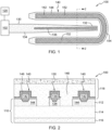
- FIG. 1 shows a schematic top-down view of a PIC 100
- FIG. 2 shows a cross-sectional view of PIC 100 along view line 2-2 in FIG. 1
- PIC 100 includes a photonic component 102 ( FIGS. 1 and 3 only for clarity purposes) on or in a semiconductor substrate 110.
- Semiconductor substrate 110 may include any now known or later developed semiconductor substrate.
- semiconductor substrate 110 includes a layered semiconductor-insulator-semiconductor substrate in place of a more conventional silicon substrate (bulk substrate). As shown in FIG.
- semiconductor substrate 110 includes a semiconductor-on-insulator (SOI) substrate including a semiconductor layer 112 (e.g., an active semiconductor layer) over a buried insulator layer 114 over a base semiconductor layer 116.
- semiconductor layer 112 e.g., an active semiconductor layer
- base semiconductor layer 116 may include but are not limited to: silicon, germanium, silicon germanium, silicon carbide.
- Buried insulator layer 114 may include any appropriate dielectric such as but not limited to silicon dioxide, i.e., forming a buried oxide (BOX) layer. A portion of or the entire semiconductor substrate may be strained. The precise thickness of buried insulating layer 114 and active SOI layer 112 may vary widely with the intended application.
- Photonic component 102 is on or in semiconductor substrate 110.
- photonic component 102 may be positioned in active SOI layer 112.
- photonic component 120 may be in any middle-of-line (MOL) or back-end-of-line (BEOL) interconnect layer 118 over semiconductor substrate 110, i.e., dielectric layer with metal wire or vias therein.
- Photonic component 102 may be any optical component such as but not limited to at least one of: a photodetector, an avalanche photodiode (APD), an optical waveguide, an optical input/output coupler, and an optical absorber.
- PIC 100 may also include an electronic component 120 ( FIGS.
- Photonic component 102 may be operatively connected and interact with electric component 120 in any now known or later developed fashion.
- electronic component 120 may be any passive or active device including, e.g., transistors with contacts and metal wiring layers, etc.
- Waveguide 130 is optically coupled to photonic component 102 to receive/transmit optical signals to photonic component 102.
- the optical signals typically, but not necessarily, travel in a plane of semiconductor substrate 110 or parallel to semiconductor substrate 110.
- Optical signals traveling outside of waveguide 130 are considered undesired or harmful ⁇ stray optical signals' or ⁇ optical noise.
- Waveguide 130 is in or over semiconductor substrate 110.
- waveguide 130 can take a variety of material forms according to embodiments of the disclosure.
- waveguide 130 includes a terminal end 132. Terminal end 132 is a location at which it is desired to minimize stray optical signals.
- PIC 100 includes an optical absorber 140 having a curved shape adjacent to opposing sides and an endwall of terminal end 132 of waveguide 130. That is, optical absorber 140 has a curved shape that surrounds terminal end 132 of waveguide 130.
- Optical absorber 140 is multi-layered and includes a light absorbing layer 142 over a silicon layer 144.
- Light absorbing layer 142 may have a light absorbing coefficient that is greater than the light absorbing coefficient of silicon for a given wavelength range.
- the light absorbing layer 142 may include germanium or a vanadate.
- a germanium-including layer 142 of optical absorber 140 may include crystalline germanium (see e.g., FIG. 2 ), polycrystalline germanium (see e.g., FIG.
- a vanadate-including layer 142 may include a vanadate-based material (i.e., including vanadium and oxygen) such as but not limited to: calcium vanadate (CaVO 3 ) or strontium vanadate (SrVO 3 ). It will be recognized that silicon may also constitute a light absorbing layer.
- a vanadate-based material i.e., including vanadium and oxygen
- CaVO 3 calcium vanadate
- strontium vanadate SrVO 3
- silicon may also constitute a light absorbing layer.
- optical absorber 140 may include a capping layer 146 (labeled in FIG. 2 only for clarity) of, e.g., silicon nitride or other conventional capping materials, thereover.
- Optical waveguide 140 is generally linear immediately upstream of terminal end 132 but, as will be described, may have some turns therein in some embodiments.
- Optical absorber 140 has a curved shaped configured to absorb stray optical signals from terminal end 132 of waveguide 130 to prevent stray optical signals from creating operational problems for any photonic components 102 in PIC 100.
- optical absorber 140 may have a U-shape having a pair of legs 152 extending from a bight portion 154. Terminal end 132 of waveguide 130 is aimed into bight portion 154, such that any stray optical signals coming linearly out of terminal end 132 are directed into bight portion 154.
- Bight portion 154 can have any curved shape such as a concave shape (facing terminal end 132) that can connect legs 152. In this manner, any stray optical signals coming out of terminal end 132 are absorbed by optical absorber 140. Legs 152 may extend along sides of waveguide 130 to any desired length to absorb stray optical signals escaping from sides of waveguide 130 or otherwise escaping absorption by bight portion 154. In FIG. 1 , pair of legs 152 are linear. In other embodiments, as shown for example in FIG. 3 , pair of legs 152 may flare outwardly away from waveguide 130 near respective ends of the legs. That is, legs 152 flare outwardly away from waveguide 130 near respective ends of the legs. While bight portion 154 is shown as convex on an outer side (right side as shown), bight portion 154 can have any desired outer shape.
- Waveguide 130 can take a variety of material forms.
- waveguide 130 includes a first portion 134 of one of silicon and silicon nitride and a second portion 136 of a light absorbing material, e.g., germanium or a vanadate, positioned over first portion 134 and/or under first portion 134.
- a light absorbing material e.g., germanium or a vanadate
- first portion 134 includes silicon in SOI layer 112
- second portion 136 includes germanium or a vanadate positioned over first portion 134 (and perhaps, but not necessarily, partially in first portion 134).
- FIG. 4 shows a cross-sectional view of PIC 100 (e.g., along view line 4-4 in FIG. 9 ) including optical absorber 140, according to other embodiments of the disclosure.
- first portion 134 of waveguide 130 includes silicon nitride and second portion 136 of waveguide 130 includes a light absorbing material, e.g., germanium or a vanadate, positioned over first portion 134 and/or under first portion 134 (under shown with dashed box).
- First portion 134 of silicon nitride (and second portion(s) 136) is located in any MOL or BEOL interconnect layer 118.
- waveguide 130 includes a silicon nitride 160 (e.g., in any MOL or BEOL interconnect layer 118) over silicon 162 in active SOI layer 112.
- the dielectric of interconnect layers 118 may separate silicon nitride 160 and silicon 162.
- waveguide 130 may include silicon 164 in active SOI layer 112.
- waveguide 130 may include silicon nitride 166 above active SOI layer 112, i.e., in any MOL or BEOL interconnect layer 118.
- FIG. 9 and 10 waveguide 130 may include silicon nitride 166 above active SOI layer 112, i.e., in any MOL or BEOL interconnect layer 118.
- waveguide 130 may include amorphous silicon 170 in active SOI layer 112.
- waveguide 130 may include polysilicon 172 above active SOI layer 112, e.g., in any MOL or BEOL interconnect layer 118.
- waveguide 130 may include polysilicon 174 (e.g., in any MOL or BEOL interconnect layer 118) over silicon 176 in active SOI layer 112.
- Waveguide 130 can have a variety of horizontal arrangements. In most embodiments, as shown for example in FIG. 9 , waveguide 130 has a tapering width (vertical on page) along at least a portion of a length (horizontal on page) thereof with terminal end 132 having a smallest width.
- first portion 134 i.e., silicon
- second portion 136 i.e., germanium or a vanadate
- first portion 134 tapers in width as it approaches terminal end 132
- second portion 136 enlarges in width at it approaches terminal end 132.
- the taper can also be reversed in direction.
- waveguide 130 may have a sinusoidal path 180 along a portion of a length thereof.
- terminal end 132 is aimed into bight portion 154 of optical absorber 140.
- sinusoidal path 180 is shown relative to waveguide 130 with silicon in active SOI layer 112, it may be applied to any waveguide 130 material arrangement described herein.
- FIG. 17 and 18 show waveguide 130 with just a fishbone portion 186.
- Portions 184, 186 can taper in width (vertical on page) in any manner desired.
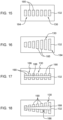
- FIG. 15 shows segmented portion 184 with segments 185 of equal width (vertical on page)
- FIG. 16 shows segmented portion 184 with segments 185 of that are gradually wider (vertical on page) closer to terminal end 132.
- FIG. 17 shows fishbone segment 186 with ribs 190 of equal length
- FIG. 18 shows fishbone portion 186 with ribs 190 of that are gradually wider (vertical on page) closer to terminal end 132.
- FIG. 19 shows a sectioned waveguide 230 with a solid portion 182 and a fishbone portion 186, but no segmented portion 184 ( FIGS. 13-16 ).
- optical absorber 140 has been shown to include a single light absorbing layer 142, in certain embodiments, light absorbing layer 142 can be arranged in a large variety of vertically and/or horizontally segmented arrangements.
- a plurality of light absorbing layers 142 may be used over silicon layer 144 in optical waveguide 140. That is, optical absorber 140 may include a plurality of vertically spaced or segmented light absorbing layers 142 (germanium-including or a vanadate-including layer), e.g., with an interlayer dielectric of interconnect layers 118 therebetween.
- Light absorbing layer 142 of optical absorber 140 may also be segmented in a horizontal arrangement along a length of optical absorber 140.
- FIG. 23 shows a top-down view and FIG. 24 shows a cross-sectional view along view line 24-24 in FIG. 23 of PIC 100, according to another embodiment.
- optical absorber 140 may include a pair of nested optical absorbers 140A, 140B. Each optical absorber 140A, 140B has the curved shape surrounding terminal end 132 of waveguide 130, 230.
- Optical absorber 140B may have a larger bight portion 154B, e.g., longer between legs 152B, to accommodate bight portion 154A of optical absorber 140A therein.
- Each optical absorber 140A, 140B is shown including light absorbing layer 142 (of a germanium-including or a vanadate-including material) over silicon layer 144.
- optical absorbers 140A, 140B can take any form described herein. While a pair of optical absorbers 140A, 140B are illustrated, more than two optical absorbers may be nested in a similar manner to that shown.
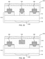
- FIGS. 25 and 26 show cross-sectional views PIC 100 according to alternative embodiments.
- PIC 100 may further include an undercut or void 200 in base semiconductor layer 116 under waveguide 130, i.e., under buried insulator layer 114.
- Undercut 200 may further prevent stray optical signals from traveling into base semiconductor layer 116 from waveguide 130.
- Undercut 200 may be located under at least a portion of waveguide 130, e.g., under terminal end 132. While shown used with just two embodiments, undercut 200 can be used in any embodiment described herein.
- PIC 100 may include waveguide 130 in or over semiconductor substrate 110.
- Waveguide 130 includes first portion 134 of one of silicon (see e.g., FIG. 2 ) and silicon nitride (see e.g., FIG. 4 ) and second portion 136 of germanium positioned at least over first portion 134 ( FIGS. 2 and 4 ) or under first portion 134 (dashed version in FIG. 4 ).
- waveguide 130 is linear and has terminal end 132.
- FIG. 1 waveguide 130 is linear and has terminal end 132.
- first portion 134 of waveguide 130 has a tapering width (vertical on page) along a length thereof with terminal end 132 having the smallest width of first portion 134
- second portion 136 of waveguide 130 has an enlarging width (vertical on page) along a length thereof with terminal end 132 having the largest width of second portion 136.
- Optical absorber 140 has a curved shape surrounding terminal end 132 of waveguide 130 and includes a light absorbing layer 142 over silicon layer 144.
- a germanium-including light absorbing layer 142 of optical absorber 140 may include crystalline germanium (see e.g., FIG. 2 ), polycrystalline germanium (see e.g., FIG. 20 ) or amorphous germanium ( FIGS. 2 or 20 ).
- a vanadate-including light absorbing layer 142 may include a vanadate-based material (i.e., including vanadium and oxygen) such as but not limited to: calcium vanadate (CaVOs) or strontium vanadate (SrVO 3 ).
- Optical absorber 140 has a U-shape having pair of legs 152 extending from bight portion 154. Terminal end 132 of waveguide 130 is aimed into bight portion 154, and pair of legs 152 may flare outwardly away from waveguide 130 near respective ends of legs 152. As shown in FIGS. 23 and 24 , optical absorber 140 may include a pair of nested optical absorbers 140A, 140B. Each optical absorber 140A, 140B has the curved shape surrounding terminal end 132 of waveguide 130, 230. Each optical absorber 140A, 140B is includes light absorbing layer 142 (germanium-including or a vanadate-including layer) over silicon layer 144.
- light absorbing layer 142 germanium-including or a vanadate-including layer
- adjacent portions of the terminal end of the waveguide and the optical absorber must be sufficiently close and mode matching must occur at location(s) along the adjacent portions (i.e., there must be at least one location where the propagation constant of optical mode inside the two adjacent portions is the same).
- the optical mode of light is generally determined by refractive index profile of the waveguide core and its cross-sectional geometric size and shape.
- mode matching generally occurs at a location where the cross-sectional areas of the adjacent portions of the waveguide cores are approximately the same. If waveguide cores are made of different core materials with different refractive index profiles, mode matching can occur at a location where adjacent portions of waveguide cores have different cross-sectional areas but the same propagation constant which is determined by the respective combinations of refractive index and cross-sectional area. When the sizes and/or the materials of the waveguide cores are different, these differences must be accounted for in order to achieve mode matching.
- Tapering of the terminal end of the waveguide and/or tapering of the legs of the light absorber can be employed to increase the likelihood that mode matching will occur between adjacent portions of the terminal end of the waveguide and of the light absorber that are made of different materials and/or sizes and/or in the presences of process variations.
- a method of forming PIC 100 may include forming waveguide 130, 230 in or over semiconductor substrate 110. As noted, waveguide 130, 230 has terminal end 132. The method may also include forming optical absorber 140 having a curved shape surrounding terminal end 132 of waveguide 130, 230. Optical absorber 140 includes light absorbing layer 142 (germanium-including or a vanadate-including layer) over silicon layer 144. Waveguide 130, 230 and optical absorber(s) 140 can be formed using any now known or later developed semiconductor fabrication techniques.
- the optical absorber reduces optical noise and provides performance improvements for functional components and circuits (e.g., dark current reduction, scattering loss reduction).
- the optical absorber is fully compatible with current semiconductor process flows and does not require additional layers and/or process steps.
- the optical absorber can be placed in any area where stray optical signals (light scattering) are anticipated from a terminal end of a waveguide, such as but not limited to near sensitive photonic components such as photodetectors and/or optical modulators.
- the structure and method as described above are used in the fabrication of integrated circuit and photonic integrated circuit chips.
- the resulting chips can be distributed by the fabricator in raw wafer form (that is, as a single wafer that has multiple unpackaged chips), as a bare die, or in a packaged form.
- the chip is mounted in a single chip package (such as a plastic carrier, with leads that are affixed to a motherboard or other higher-level carrier) or in a multichip package (such as a ceramic carrier that has either or both surface interconnections or buried interconnections).
- the chip is then integrated with other chips, discrete circuit elements, and/or other signal processing devices as part of either (a) an intermediate product, such as a motherboard, or (b) an end product.
- the end product can be any product that includes integrated circuit chips, ranging from toys and other low-end applications to advanced computer products having a display, a keyboard or other input device, and a central processor.
- a photonic integrated circuit including a waveguide in or over a semiconductor substrate.
- the waveguide has a terminal end.
- the PIC also includes an optical absorber having a curved shape adjacent to opposing sides and an endwall of the terminal end of the waveguide, i.e., it surrounds the terminal end of the waveguide.
- the optical absorber is multi-layered and includes a light absorbing layer.
- the light absorbing layer may include germanium or a vanadate.
- the optical absorber terminates or attenuates any stray optical signals from the waveguide while maintaining low back reflection.
- a photonic integrated circuit comprising:
- the optical absorber includes the light absorbing layer over a silicon layer and the light absorbing layer includes one of a germanium material and a vanadate material, that is a material comprising germanium or the material being germanium and a material comprising vandate or the material being vandate.
- germanium material of the optical absorber includes one of crystalline germanium, polycrystalline germanium and amorphous germanium, and/or wherein the vanadate material of the optical absorber includes one of calcium vanadate and strontium vanadate.
- optical absorber has a U-shape having a pair of legs extending from a bight portion, wherein the terminal end of the waveguide is aimed into the bight portion.
- each optical absorber includes a pair of nested optical absorbers, each optical absorber having the curved shape surrounding the terminal end of the waveguide, each optical absorber includes the light absorbing layer over a silicon layer.
- the waveguide has a layout chosen from a group comprising: a solid peg layout, a segmented fishbone layout and a combination peg and segmented fishbone layout.
- the semiconductor substrate includes a semiconductor-on-insulator (SOI) substrate including an semiconductor layer over a buried insulator layer over a base semiconductor layer, and further comprising an undercut in the base semiconductor layer under the waveguide.
- SOI semiconductor-on-insulator
- the semiconductor substrate includes a semiconductor-on-insulator (SOI) substrate including an semiconductor layer over a buried insulator layer over a base semiconductor layer
- the waveguide includes one of: silicon in a semiconductor layer; silicon nitride over silicon in the semiconductor layer; silicon nitride above the semiconductor layer; amorphous silicon in the semiconductor layer; polysilicon above the semiconductor layer; and polysilicon over silicon in the semiconductor layer.
- the waveguide includes a first portion of one of silicon and silicon nitride and a second portion of the light absorbing layer positioned at least over the first portion or under the first portion.
- the first portion of the waveguide for example the silicon of the waveguide
- the second portion or the light absorbing layer of the waveguide has an enlarging width along a length thereof with the terminal end having a largest width of the second portion or the light absorbing layer.
- the first portion of the waveguide may have a tapering width along a length thereof with the terminal end having a smallest width of the first portion
- the second portion of the waveguide may have an enlarging width along a length thereof with the terminal end having a largest width of the second portion.
- the silicon of the waveguide may have a tapering width along a length thereof with the terminal end having a smallest width of the silicon
- the light absorbing layer of the waveguide may have an enlarging width along a length thereof with the terminal end having a largest width of the light absorbing layer
- the waveguide comprises a first portion of one of silicon and silicon nitride and a second portion of germanium positioned at least over the first portion or under the first portion, the waveguide being linear, each optical absorber preferably comprising the light absorbing layer over the silicon layer, and wherein the optical absorber having the curved shape with the curved shape surrounding the terminal end of the waveguide, the light absorbing layer being formed over a silicon layer, wherein the light absorbing layer includes one of a germanium material and a vanadate material.
- a photonic integrated circuit comprising:
- the PIC of embodiment 15 or 16 wherein the first portion of the waveguide has a tapering width along a length thereof with the terminal end having a smallest width of the first portion, and the second portion of the waveguide has an enlarging width along a length thereof with the terminal end having a largest width of the second portion.
- Embodiment 19 The PIC of one of embodiments 15 to 18, wherein the optical absorber has a U-shape having a pair of legs extending from a bight portion, wherein the terminal end of the waveguide is aimed into the bight portion, and wherein the pair of legs flare outwardly away from the waveguide near respective ends thereof.
- each optical absorber includes a pair of nested optical absorbers, each optical absorber having the curved shape surrounding the terminal end of the waveguide, each optical absorber includes the light absorbing layer over the silicon layer.
- the PIC of one of embodiments 1 to 20 may be formed.
- the term "include” and its variants may be interpreted as meaning that an embodiment includes stated features, while not necessarily excluding the presence of other features that are not explicitly stated.
Landscapes
- Physics & Mathematics (AREA)
- Engineering & Computer Science (AREA)
- Microelectronics & Electronic Packaging (AREA)
- General Physics & Mathematics (AREA)
- Optics & Photonics (AREA)
- Power Engineering (AREA)
- Optical Integrated Circuits (AREA)
Abstract
A photonic integrated circuit (PIC) includes a waveguide in or over a semiconductor substrate. The waveguide has a terminal end. The PIC also includes an optical absorber having a curved shape adjacent to opposing sides and an endwall of the terminal end of the waveguide, i.e., it surrounds the terminal end of the waveguide. The optical absorber is multi-layered and includes a light absorbing layer. The light absorbing layer may include germanium or a vanadate. The optical absorber terminates or attenuates any stray optical signals from the waveguide while maintaining low back reflection.
Description
- The present disclosure relates to semiconductor structures and, more particularly, to a photonic integrated circuit structure including an optical absorber for a terminal end of a waveguide and methods of manufacture.
- Photonic integrated circuits (PICs) can be made using existing semiconductor fabrication techniques, and because silicon is already used as the substrate for most integrated circuits, it is possible to create hybrid devices in which the optical and electronic components are integrated onto a single microchip. PICs include a variety of photonic components that receive and/or output optical signals. Certain optical components in a PIC, such as optical waveguides, optical input/output couplers, laser couplers, among others, can create stray optical signals. The stray optical signals are scattered through the PIC and create background optical noise. The stray optical signals received by an unintended photonic component, e.g., a photodetector, may create operational problems for that component. Spiral optical absorbers are used to capture stray optical signals, but they have a very large footprint, and may scatter the optical signal into neighboring structure.
- All aspects, examples and features mentioned below can be combined in any technically possible way.
- An aspect of the disclosure provides a photonic integrated circuit (PIC), comprising: a waveguide in or over a semiconductor substrate, the waveguide having a terminal end; and an optical absorber having a curved shape adjacent to opposing sides and an endwall of the terminal end of the waveguide, the optical absorber is multi-layered and includes a light absorbing layer.
- An aspect of the disclosure provides a photonic integrated circuit (PIC), comprising: a waveguide in or over a semiconductor substrate, the waveguide including a first portion of one of silicon and silicon nitride and a second portion of a light absorbing layer positioned at least over the first portion or under the first portion, and wherein the waveguide is linear and has a terminal end; and an optical absorber having a curved shape surrounding the terminal end of the waveguide, the optical absorber includes a light absorbing layer over a silicon layer, wherein the light absorbing layer includes one of germanium and a vanadate.
- An aspect of the disclosure provides a method of forming a photonic integrated circuit (PIC), the method comprising: forming a waveguide in or over a semiconductor substrate, the waveguide having a terminal end; and forming an optical absorber having a curved shape surrounding the terminal end of the waveguide, the optical absorber includes a light absorbing layer over a silicon layer, wherein the light absorbing layer includes one of germanium and a vanadate.
- Two or more aspects described in this disclosure, including those described in this summary section, may be combined to form implementations not specifically described herein. The details of one or more implementations are set forth in the accompanying drawings and the description below. Other features, objects and advantages will be apparent from the description and drawings, and from the claims.
- The embodiments of this disclosure will be described in detail, with reference to the following figures, wherein like designations denote like elements, and wherein:
-
FIG. 1 shows a top-down view of a photonic integrated circuit (PIC) including an optical absorber, according to embodiments of the disclosure; -
FIG. 2 shows a cross-sectional view of the PIC including the optical absorber along view line 2-2 inFIG. 1 , according to embodiments of the disclosure; -
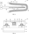
FIG. 3 shows a top-down view of PIC including an optical absorber, according to other embodiments of the disclosure; -
FIG. 4 shows a cross-sectional view of the PIC including the optical absorber, according to other embodiments of the disclosure; -
FIG. 5 shows a top-down view of a PIC including an optical absorber, according to embodiments of the disclosure; -
FIG. 6 shows a cross-sectional view of the PIC including the optical absorber along view line 6-6 inFIG. 5 , according to embodiments of the disclosure; -
FIG. 7 shows a top-down view of a PIC including an optical absorber, according to embodiments of the disclosure; -
FIG. 8 shows a cross-sectional view of the PIC including the optical absorber along view line 8-8 inFIG. 7 , according to embodiments of the disclosure; -
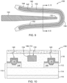
FIG. 9 shows a top-down view of a PIC including an optical absorber, according to embodiments of the disclosure; -
FIG. 10 shows a cross-sectional view of the PIC including the optical absorber along view line 10-10 inFIG. 9 , according to embodiments of the disclosure; -
FIG. 11 shows a top-down view of a PIC including an optical absorber, according to embodiments of the disclosure; -
FIG. 12 shows a cross-sectional view of the PIC including the optical absorber along view line 12-12 inFIG. 11 , according to embodiments of the disclosure; -
FIG. 13 shows a top-down view of a PIC including an optical absorber, according to other embodiments of the disclosure; -
FIG. 14 shows a top-down view of a PIC including an optical absorber, according to additional embodiments of the disclosure; -
FIG. 15 shows a top-down view of a waveguide, according to other embodiments of the disclosure; -
FIG. 16 shows a top-down view of a waveguide, according to other embodiments of the disclosure; -
FIG. 17 shows a top-down view of a waveguide, according to other embodiments of the disclosure; -
FIG. 18 shows a top-down view of a waveguide, according to other embodiments of the disclosure; -
FIG. 19 shows a top-down view of a waveguide, according to other embodiments of the disclosure; -
FIG. 20 shows a cross-sectional view of a PIC including an optical absorber, according to other embodiments of the disclosure; -
FIG. 21 shows a cross-sectional view of a PIC including an optical absorber, according to other embodiments of the disclosure; -
FIG. 22 shows a top-down view of an optical absorber, according to other embodiments of the disclosure; -
FIG. 23 shows a top-down view of a PIC including an optical absorber, according to embodiments of the disclosure; -
FIG. 24 shows a cross-sectional view of the PIC including the optical absorber along view line 24-24 inFIG. 23 , according to embodiments of the disclosure; -
FIG. 25 shows a cross-sectional view of a PIC including an optical absorber, according to other embodiments of the disclosure; and -
FIG. 26 shows a cross-sectional view of a PIC including an optical absorber, according to additional embodiments of the disclosure. - It is noted that the drawings of the disclosure are not necessarily to scale. The drawings are intended to depict only typical aspects of the disclosure, and therefore should not be considered as limiting the scope of the disclosure. In the drawings, like numbering represents like elements between the drawings.
- In the following description, reference is made to the accompanying drawings that form a part thereof, and in which is shown by way of illustration specific illustrative embodiments in which the present teachings may be practiced. These embodiments are described in sufficient detail to enable those skilled in the art to practice the present teachings, and it is to be understood that other embodiments may be used and that changes may be made without departing from the scope of the present teachings. The following description is, therefore, merely illustrative.
- It will be understood that when an element such as a layer, region, or substrate is referred to as being "on" or "over" another element, it may be directly on the other element or intervening elements may also be present. In contrast, when an element is referred to as being "directly on" or "directly over" another element, there may be no intervening elements present. It will also be understood that when an element is referred to as being "connected" or "coupled" to another element, it may be directly connected or coupled to the other element or intervening elements may be present. In contrast, when an element is referred to as being "directly connected" or "directly coupled" to another element, there are no intervening elements present.
- Reference in the specification to "one embodiment" or "an embodiment" of the present disclosure, as well as other variations thereof, means that a particular feature, structure, characteristic, and so forth described in connection with the embodiment is included in at least one embodiment of the present disclosure. Thus, the phrases "in one embodiment" or "in an embodiment," as well as any other variations appearing in various places throughout the specification are not necessarily all referring to the same embodiment. It is to be appreciated that the use of any of the following "/," "and/or," and "at least one of," for example, in the cases of "A/B," "A and/or B" and "at least one of A and B," is intended to encompass the selection of the first listed option (A) only, or the selection of the second listed option (B) only, or the selection of both options (A and B). As a further example, in the cases of "A, B, and/or C" and "at least one of A, B, and C," such phrasing is intended to encompass the first listed option (A) only, or the selection of the second listed option (B) only, or the selection of the third listed option (C) only, or the selection of the first and the second listed options (A and B), or the selection of the first and third listed options (A and C) only, or the selection of the second and third listed options (B and C) only, or the selection of all three options (A and B and C). This may be extended, as readily apparent by one of ordinary skill in the art, for as many items listed.
- Embodiments of the disclosure include a photonic integrated circuit (PIC). The PIC includes a waveguide in or over a semiconductor substrate. The waveguide has a terminal end. The PIC also includes an optical absorber having a curved shape adjacent to opposing sides and an endwall of the terminal end of the waveguide, i.e., it surrounds the terminal end of the waveguide. The optical absorber includes a light absorbing layer over a silicon layer. The light absorbing layer includes germanium or a vanadate. The optical absorber terminates or attenuates stray optical signals from the waveguide while maintaining low back reflection.
-
FIG. 1 shows a schematic top-down view of aPIC 100, andFIG. 2 shows a cross-sectional view ofPIC 100 along view line 2-2 inFIG. 1 . (Note,FIG. 1 showslayers FIG. 2 ).PIC 100 includes a photonic component 102 (FIGS. 1 and3 only for clarity purposes) on or in asemiconductor substrate 110.Semiconductor substrate 110 may include any now known or later developed semiconductor substrate. In the non-limiting example shown,semiconductor substrate 110 includes a layered semiconductor-insulator-semiconductor substrate in place of a more conventional silicon substrate (bulk substrate). As shown inFIG. 2 ,semiconductor substrate 110 includes a semiconductor-on-insulator (SOI) substrate including a semiconductor layer 112 (e.g., an active semiconductor layer) over a buriedinsulator layer 114 over abase semiconductor layer 116. Semiconductor layer 112 (hereafter "active SOI layer 112" for brevity) andbase semiconductor layer 116 may include but are not limited to: silicon, germanium, silicon germanium, silicon carbide. Buriedinsulator layer 114 may include any appropriate dielectric such as but not limited to silicon dioxide, i.e., forming a buried oxide (BOX) layer. A portion of or the entire semiconductor substrate may be strained. The precise thickness of buried insulatinglayer 114 andactive SOI layer 112 may vary widely with the intended application. -
Photonic component 102 is on or insemiconductor substrate 110. In certain embodiments,photonic component 102 may be positioned inactive SOI layer 112. In other embodiments,photonic component 120 may be in any middle-of-line (MOL) or back-end-of-line (BEOL)interconnect layer 118 oversemiconductor substrate 110, i.e., dielectric layer with metal wire or vias therein.Photonic component 102 may be any optical component such as but not limited to at least one of: a photodetector, an avalanche photodiode (APD), an optical waveguide, an optical input/output coupler, and an optical absorber.PIC 100 may also include an electronic component 120 (FIGS. 1 and3 only for clarity purposes), which may be formed, for example, inactive SOI layer 112, e.g., at a location other than wherephotonic component 102 is located.Photonic component 102 may be operatively connected and interact withelectric component 120 in any now known or later developed fashion. In embodiments,electronic component 120 may be any passive or active device including, e.g., transistors with contacts and metal wiring layers, etc. -
PIC 100 includes an optical waveguide 130 (hereafter "waveguide 130").Waveguide 130 is optically coupled tophotonic component 102 to receive/transmit optical signals tophotonic component 102. The optical signals typically, but not necessarily, travel in a plane ofsemiconductor substrate 110 or parallel tosemiconductor substrate 110. Optical signals traveling outside ofwaveguide 130 are considered undesired or harmful `stray optical signals' or `optical noise.'Waveguide 130 is in or oversemiconductor substrate 110. As will be described further herein,waveguide 130 can take a variety of material forms according to embodiments of the disclosure. In any event,waveguide 130 includes aterminal end 132.Terminal end 132 is a location at which it is desired to minimize stray optical signals. To this end,PIC 100 includes anoptical absorber 140 having a curved shape adjacent to opposing sides and an endwall ofterminal end 132 ofwaveguide 130. That is,optical absorber 140 has a curved shape that surroundsterminal end 132 ofwaveguide 130.Optical absorber 140 is multi-layered and includes a lightabsorbing layer 142 over asilicon layer 144. Lightabsorbing layer 142 may have a light absorbing coefficient that is greater than the light absorbing coefficient of silicon for a given wavelength range. In some embodiments, thelight absorbing layer 142 may include germanium or a vanadate. A germanium-includinglayer 142 ofoptical absorber 140 may include crystalline germanium (see e.g.,FIG. 2 ), polycrystalline germanium (see e.g.,FIG. 20 ) or amorphous germanium (FIG. 2 or20 ). A vanadate-includinglayer 142 may include a vanadate-based material (i.e., including vanadium and oxygen) such as but not limited to: calcium vanadate (CaVO3) or strontium vanadate (SrVO3). It will be recognized that silicon may also constitute a light absorbing layer. - As shown in
FIGS. 1 and 2 , where light absorbinglayer 142 is in a middle-of-line (MOL) dielectric layer 148 (FIG. 2 ) ofinterconnect layers 118, i.e., immediately aboveactive SOI layer 112, it may include crystalline germanium (c-Ge). Otherwise, as will be described further herein, where light absorbinglayer 142 is in a back-end-of-line (BEOL) dielectric layer 150 (FIG. 4 ) ofinterconnect layers 118, i.e., not immediately aboveactive SOI layer 112, it may include a polycrystalline germanium.Silicon layer 144 may be inactive SOI layer 112. In certain embodiments,optical absorber 140 may include a capping layer 146 (labeled inFIG. 2 only for clarity) of, e.g., silicon nitride or other conventional capping materials, thereover. -
Optical waveguide 140 is generally linear immediately upstream ofterminal end 132 but, as will be described, may have some turns therein in some embodiments.Optical absorber 140 has a curved shaped configured to absorb stray optical signals fromterminal end 132 ofwaveguide 130 to prevent stray optical signals from creating operational problems for anyphotonic components 102 inPIC 100. As shown inFIG. 1 ,optical absorber 140 may have a U-shape having a pair oflegs 152 extending from abight portion 154.Terminal end 132 ofwaveguide 130 is aimed intobight portion 154, such that any stray optical signals coming linearly out ofterminal end 132 are directed intobight portion 154.Bight portion 154 can have any curved shape such as a concave shape (facing terminal end 132) that can connectlegs 152. In this manner, any stray optical signals coming out ofterminal end 132 are absorbed byoptical absorber 140.Legs 152 may extend along sides ofwaveguide 130 to any desired length to absorb stray optical signals escaping from sides ofwaveguide 130 or otherwise escaping absorption bybight portion 154. InFIG. 1 , pair oflegs 152 are linear. In other embodiments, as shown for example inFIG. 3 , pair oflegs 152 may flare outwardly away fromwaveguide 130 near respective ends of the legs. That is,legs 152 flare outwardly away fromwaveguide 130 near respective ends of the legs. Whilebight portion 154 is shown as convex on an outer side (right side as shown),bight portion 154 can have any desired outer shape. - Further embodiments described herein illustrate a wide variety of
waveguide 130 andoptical absorber 140 options. It is emphasized that while each drawing shows certain aspects ofwaveguide 130 andoptical waveguide 140, the various features of each part can be used together in any combination, including those not expressly illustrated. - Variations of waveguides will now be described.
Waveguide 130 can take a variety of material forms. In certain embodiments, as shown inFIGS. 1-3 ,waveguide 130 includes afirst portion 134 of one of silicon and silicon nitride and asecond portion 136 of a light absorbing material, e.g., germanium or a vanadate, positioned overfirst portion 134 and/or underfirst portion 134. (As used herein, the terms "light absorbing layer" and "light absorbing material" are used to differentiate between the parts ofwaveguide 130 andoptical absorber 140, but they may be structured the same, e.g., as layers, or differently.) InFIGS. 1-2 ,first portion 134 includes silicon inSOI layer 112 andsecond portion 136 includes germanium or a vanadate positioned over first portion 134 (and perhaps, but not necessarily, partially in first portion 134). -
FIG. 4 shows a cross-sectional view of PIC 100 (e.g., along view line 4-4 inFIG. 9 ) includingoptical absorber 140, according to other embodiments of the disclosure. InFIG. 4 ,first portion 134 ofwaveguide 130 includes silicon nitride andsecond portion 136 ofwaveguide 130 includes a light absorbing material, e.g., germanium or a vanadate, positioned overfirst portion 134 and/or under first portion 134 (under shown with dashed box).First portion 134 of silicon nitride (and second portion(s) 136) is located in any MOL orBEOL interconnect layer 118. - In other embodiments, shown in
FIGS. 5 and 6 ,waveguide 130 includes a silicon nitride 160 (e.g., in any MOL or BEOL interconnect layer 118) over silicon 162 inactive SOI layer 112. The dielectric ofinterconnect layers 118 may separate silicon nitride 160 and silicon 162. In other embodiments, shown inFIGS. 7 and 8 ,waveguide 130 may include silicon 164 inactive SOI layer 112. In other embodiments, shown inFIGS. 9 and 10 ,waveguide 130 may include silicon nitride 166 aboveactive SOI layer 112, i.e., in any MOL orBEOL interconnect layer 118. In other embodiments, as also shown inFIG. 8 ,waveguide 130 may include amorphous silicon 170 inactive SOI layer 112. In other embodiments, as also shown inFIG. 10 ,waveguide 130 may include polysilicon 172 aboveactive SOI layer 112, e.g., in any MOL orBEOL interconnect layer 118. In other embodiments, as also shown inFIG. 6 ,waveguide 130 may include polysilicon 174 (e.g., in any MOL or BEOL interconnect layer 118) over silicon 176 inactive SOI layer 112. -
Waveguide 130 can have a variety of horizontal arrangements. In most embodiments, as shown for example inFIG. 9 ,waveguide 130 has a tapering width (vertical on page) along at least a portion of a length (horizontal on page) thereof withterminal end 132 having a smallest width. InFIGS. 1-4 , first portion 134 (i.e., silicon) ofwaveguide 130 has a tapering width (vertical on page) along a length (horizontal on page) thereof withterminal end 132 having a smallest width of the silicon, and second portion 136 (i.e., germanium or a vanadate) ofwaveguide 130 has an enlarging width along a length thereof withterminal end 132 having a largest width of the light absorbing material. Hence,first portion 134 tapers in width as it approachesterminal end 132, andsecond portion 136 enlarges in width at it approachesterminal end 132. The taper can also be reversed in direction. - As shown in the top-down view of
FIG. 11 and cross-sectional view ofFIG. 12 ,waveguide 130 may have asinusoidal path 180 along a portion of a length thereof. In any event,terminal end 132 is aimed intobight portion 154 ofoptical absorber 140. Whilesinusoidal path 180 is shown relative towaveguide 130 with silicon inactive SOI layer 112, it may be applied to anywaveguide 130 material arrangement described herein. -
Waveguide 130 may be solid along its length (horizontal on page), which may be referred to as a solid peg layout. Alternatively, as shown in the top-down views ofFIGS. 13-18 , a sectionedwaveguide 230 may include at least one section that is segmented in some way.FIGS. 13 and 14 show top-down views of sectionedwaveguides 230 with a respectiveoptical absorber 140, andFIGS. 15-18 show just sectionedwaveguides 230.FIGS. 13 and 14 show a combination peg and segmented fishbone layout. In these embodiments, sectionedwaveguide 230 includes a solid portion 182 (i.e., solid peg, perhaps but not necessarily tapered), a segmented portion 184 (i.e., with individually spacedsegments 185 with a dielectric ofinterconnect layers 118 therebetween), and afishbone portion 186.Fishbone portion 186 includes a smaller solid peg with ribs that resembles a fishbone. More particularly,fishbone portion 186 can include a spine 188 (not as wide as solid portion 182) andribs 190 extending fromspine 188. Any number ofribs 190 may be used.FIGS. 15 and 16 show sectionedwaveguide 230 with just asegmented portion 184, andFIGS. 17 and 18 show waveguide 130 with just afishbone portion 186.Portions FIG. 15 shows segmentedportion 184 withsegments 185 of equal width (vertical on page), andFIG. 16 shows segmentedportion 184 withsegments 185 of that are gradually wider (vertical on page) closer toterminal end 132.FIG. 17 showsfishbone segment 186 withribs 190 of equal length, andFIG. 18 showsfishbone portion 186 withribs 190 of that are gradually wider (vertical on page) closer toterminal end 132.FIG. 19 shows a sectionedwaveguide 230 with asolid portion 182 and afishbone portion 186, but no segmented portion 184 (FIGS. 13-16 ). - Variations of
optical absorber 140 will now be described. Whilewaveguide optical absorber 140 have been shown nearactive SOI layer 112,waveguide BEOL interconnect layer 118.FIG. 20 shows a cross-sectional view of an illustrative waveguide 130 (could be any form described herein) andoptical absorber 140 in aBEOL dielectric layer 150. In this example,waveguide 130 includes silicon nitride, andoptical absorber 140 includes just lightabsorbing layer 142. Where light absorbinglayer 142 is inBEOL dielectric layer 150 ofinterconnect layers 118, i.e., not immediately aboveactive SOI layer 112, it may include a polycrystalline germanium. Any number of vertically spacedlight absorbing layers 142 are possible in this setting. - While
optical absorber 140 has been shown to include a singlelight absorbing layer 142, in certain embodiments, light absorbinglayer 142 can be arranged in a large variety of vertically and/or horizontally segmented arrangements. In one example, as shown inFIG. 21 , a plurality of light absorbinglayers 142 may be used oversilicon layer 144 inoptical waveguide 140. That is,optical absorber 140 may include a plurality of vertically spaced or segmented light absorbing layers 142 (germanium-including or a vanadate-including layer), e.g., with an interlayer dielectric ofinterconnect layers 118 therebetween. Lightabsorbing layer 142 ofoptical absorber 140 may also be segmented in a horizontal arrangement along a length ofoptical absorber 140.FIG. 22 shows a top-down view ofoptical absorber 140 illustrated just one example of how light absorbinglayer 142 may be segmented along a length ofoptical absorber 140, e.g., with an interlayer dielectric ofinterconnect layers 118 therebetween. As will be recognized, light absorbinglayer 142 can be arranged in a large variety of alternative vertically and/or horizontally segmented arrangements to absorb any desired stray optical signals. -
FIG. 23 shows a top-down view andFIG. 24 shows a cross-sectional view along view line 24-24 inFIG. 23 ofPIC 100, according to another embodiment. InFIGS. 1-22 , only a singleoptical absorber 140 is provided. In other embodiments,optical absorber 140 may include a pair of nestedoptical absorbers optical absorber terminal end 132 ofwaveguide Optical absorber 140B may have alarger bight portion 154B, e.g., longer betweenlegs 152B, to accommodatebight portion 154A ofoptical absorber 140A therein. Eachoptical absorber silicon layer 144. However,optical absorbers optical absorbers -
FIGS. 25 and 26 showcross-sectional views PIC 100 according to alternative embodiments. Notably,PIC 100 may further include an undercut or void 200 inbase semiconductor layer 116 underwaveguide 130, i.e., under buriedinsulator layer 114. Undercut 200 may further prevent stray optical signals from traveling intobase semiconductor layer 116 fromwaveguide 130. Undercut 200 may be located under at least a portion ofwaveguide 130, e.g., underterminal end 132. While shown used with just two embodiments, undercut 200 can be used in any embodiment described herein. - With reference to
FIGS. 1, 2 and4 , in an alternative embodiment,PIC 100 may includewaveguide 130 in or oversemiconductor substrate 110.Waveguide 130 includesfirst portion 134 of one of silicon (see e.g.,FIG. 2 ) and silicon nitride (see e.g.,FIG. 4 ) andsecond portion 136 of germanium positioned at least over first portion 134 (FIGS. 2 and4 ) or under first portion 134 (dashed version inFIG. 4 ). As shown in, for example,FIG. 1 ,waveguide 130 is linear and hasterminal end 132. As shown inFIG. 1 , in certain embodiments,first portion 134 ofwaveguide 130 has a tapering width (vertical on page) along a length thereof withterminal end 132 having the smallest width offirst portion 134, andsecond portion 136 ofwaveguide 130 has an enlarging width (vertical on page) along a length thereof withterminal end 132 having the largest width ofsecond portion 136. -
Optical absorber 140 has a curved shape surroundingterminal end 132 ofwaveguide 130 and includes a lightabsorbing layer 142 oversilicon layer 144. A germanium-includinglight absorbing layer 142 ofoptical absorber 140 may include crystalline germanium (see e.g.,FIG. 2 ), polycrystalline germanium (see e.g.,FIG. 20 ) or amorphous germanium (FIGS. 2 or20 ). A vanadate-includinglight absorbing layer 142 may include a vanadate-based material (i.e., including vanadium and oxygen) such as but not limited to: calcium vanadate (CaVOs) or strontium vanadate (SrVO3).Optical absorber 140 has a U-shape having pair oflegs 152 extending frombight portion 154.Terminal end 132 ofwaveguide 130 is aimed intobight portion 154, and pair oflegs 152 may flare outwardly away fromwaveguide 130 near respective ends oflegs 152. As shown inFIGS. 23 and 24 ,optical absorber 140 may include a pair of nestedoptical absorbers optical absorber terminal end 132 ofwaveguide optical absorber silicon layer 144. - In the above-described embodiments, for stray optical signals to pass from the waveguide to the optical absorber and then be absorbed or attenuated by the light absorbing layer of the optical absorber, adjacent portions of the terminal end of the waveguide and the optical absorber must be sufficiently close and mode matching must occur at location(s) along the adjacent portions (i.e., there must be at least one location where the propagation constant of optical mode inside the two adjacent portions is the same). Those skilled in the art will recognize that the optical mode of light is generally determined by refractive index profile of the waveguide core and its cross-sectional geometric size and shape. If waveguide cores have the same refractive index profiles, mode matching generally occurs at a location where the cross-sectional areas of the adjacent portions of the waveguide cores are approximately the same. If waveguide cores are made of different core materials with different refractive index profiles, mode matching can occur at a location where adjacent portions of waveguide cores have different cross-sectional areas but the same propagation constant which is determined by the respective combinations of refractive index and cross-sectional area. When the sizes and/or the materials of the waveguide cores are different, these differences must be accounted for in order to achieve mode matching. Tapering of the terminal end of the waveguide and/or tapering of the legs of the light absorber can be employed to increase the likelihood that mode matching will occur between adjacent portions of the terminal end of the waveguide and of the light absorber that are made of different materials and/or sizes and/or in the presences of process variations.
- A method of forming
PIC 100 may include formingwaveguide semiconductor substrate 110. As noted,waveguide terminal end 132. The method may also include formingoptical absorber 140 having a curved shape surroundingterminal end 132 ofwaveguide Optical absorber 140 includes light absorbing layer 142 (germanium-including or a vanadate-including layer) oversilicon layer 144.Waveguide - It is emphasized that while each drawing shows certain aspects of
waveguide - Embodiments of the disclosure provide various technical and commercial advantages, examples of which are discussed herein. The optical absorber reduces optical noise and provides performance improvements for functional components and circuits (e.g., dark current reduction, scattering loss reduction). The optical absorber is fully compatible with current semiconductor process flows and does not require additional layers and/or process steps. The optical absorber can be placed in any area where stray optical signals (light scattering) are anticipated from a terminal end of a waveguide, such as but not limited to near sensitive photonic components such as photodetectors and/or optical modulators.
- The structure and method as described above are used in the fabrication of integrated circuit and photonic integrated circuit chips. The resulting chips can be distributed by the fabricator in raw wafer form (that is, as a single wafer that has multiple unpackaged chips), as a bare die, or in a packaged form. In the latter case the chip is mounted in a single chip package (such as a plastic carrier, with leads that are affixed to a motherboard or other higher-level carrier) or in a multichip package (such as a ceramic carrier that has either or both surface interconnections or buried interconnections). In any case the chip is then integrated with other chips, discrete circuit elements, and/or other signal processing devices as part of either (a) an intermediate product, such as a motherboard, or (b) an end product. The end product can be any product that includes integrated circuit chips, ranging from toys and other low-end applications to advanced computer products having a display, a keyboard or other input device, and a central processor.
- The terminology used herein is for the purpose of describing particular embodiments only and is not intended to be limiting of the disclosure. As used herein, the singular forms "a", "an" and "the" are intended to include the plural forms as well, unless the context clearly indicates otherwise. It will be further understood that the terms "comprises" and/or "comprising," when used in this specification, specify the presence of stated features, integers, steps, operations, elements, and/or components, but do not preclude the presence or addition of one or more other features, integers, steps, operations, elements, components, and/or groups thereof. "Optional" or "optionally" means that the subsequently described event or circumstance may or may not occur, and that the description includes instances where the event occurs and instances where it does not.
- Approximating language, as used herein throughout the specification and claims, may be applied to modify any quantitative representation that could permissibly vary without resulting in a change in the basic function to which it is related. Accordingly, a value modified by a term or terms, such as "about", "approximately" and "substantially", are not to be limited to the precise value specified. In at least some instances, the approximating language may correspond to the precision of an instrument for measuring the value. Here and throughout the specification and claims, range limitations may be combined and/or interchanged, such ranges are identified and include all the sub-ranges contained therein unless context or language indicates otherwise. "Approximately" as applied to a particular value of a range applies to both values, and unless otherwise dependent on the precision of the instrument measuring the value, may indicate +/-10% of the stated value(s).
- The corresponding structures, materials, acts, and equivalents of all means or step plus function elements in the claims below are intended to include any structure, material, or act for performing the function in combination with other claimed elements as specifically claimed. The description of the present disclosure has been presented for purposes of illustration and description, but is not intended to be exhaustive or limited to the disclosure in the form disclosed. Many modifications and variations will be apparent to those of ordinary skill in the art without departing from the scope and spirit of the disclosure. The embodiment was chosen and described in order to best explain the principles of the disclosure and the practical application, and to enable others of ordinary skill in the art to understand the disclosure for various embodiments with various modifications as are suited to the particular use contemplated.
- In summary, the above description discloses a photonic integrated circuit (PIC), including a waveguide in or over a semiconductor substrate. The waveguide has a terminal end. The PIC also includes an optical absorber having a curved shape adjacent to opposing sides and an endwall of the terminal end of the waveguide, i.e., it surrounds the terminal end of the waveguide. The optical absorber is multi-layered and includes a light absorbing layer. The light absorbing layer may include germanium or a vanadate. The optical absorber terminates or attenuates any stray optical signals from the waveguide while maintaining low back reflection.
- The following embodiments are explicitly disclosed:
- A photonic integrated circuit (PIC), comprising:
- a waveguide in or over a semiconductor substrate, the waveguide having a terminal end; and
- an optical absorber having a curved shape adjacent to opposing sides and an endwall of the terminal end of the waveguide, the optical absorber includes a light absorbing layer. For example, the optical absorber may be multi-layered.
- The PIC of embodiment 1, wherein the optical absorber includes the light absorbing layer over a silicon layer and the light absorbing layer includes one of a germanium material and a vanadate material, that is a material comprising germanium or the material being germanium and a material comprising vandate or the material being vandate.
- The PIC of
embodiment 2, wherein the germanium material of the optical absorber includes one of crystalline germanium, polycrystalline germanium and amorphous germanium, and/or wherein the vanadate material of the optical absorber includes one of calcium vanadate and strontium vanadate. - The PIC of one of embodiments 1 to 3, wherein the light absorbing layer is segmented along a length of the optical absorber.
- The PIC of one of embodiments 1 to 4, wherein the optical absorber has a U-shape having a pair of legs extending from a bight portion, wherein the terminal end of the waveguide is aimed into the bight portion.
- The PIC of embodiment 5, wherein the pair of legs flare outwardly away from the waveguide near respective ends thereof. For example, end portions of the pair of legs in the U-shape may bend outwardly with respect to waveguide.
- The PIC of one of embodiments 1 to 6, wherein the optical absorber includes a pair of nested optical absorbers, each optical absorber having the curved shape surrounding the terminal end of the waveguide, each optical absorber includes the light absorbing layer over a silicon layer.
- The PIC of one of embodiments 1 to 7, wherein the waveguide has a tapering width along a length thereof, the terminal end having a smallest width.
- The PIC of
embodiment 8, wherein the waveguide has a layout chosen from a group comprising: a solid peg layout, a segmented fishbone layout and a combination peg and segmented fishbone layout. - The PIC of one of embodiments 1 to 9, wherein the waveguide has a sinusoidal path along a portion of a length thereof.
- The PIC of one of embodiments 1 to 10, wherein the semiconductor substrate includes a semiconductor-on-insulator (SOI) substrate including an semiconductor layer over a buried insulator layer over a base semiconductor layer, and further comprising an undercut in the base semiconductor layer under the waveguide.
- The PIC of one of embodiments 1 to 11, wherein the semiconductor substrate includes a semiconductor-on-insulator (SOI) substrate including an semiconductor layer over a buried insulator layer over a base semiconductor layer, and wherein the waveguide includes one of: silicon in a semiconductor layer; silicon nitride over silicon in the semiconductor layer; silicon nitride above the semiconductor layer; amorphous silicon in the semiconductor layer; polysilicon above the semiconductor layer; and polysilicon over silicon in the semiconductor layer.
- The PIC of one of embodiments 1 to 12, wherein the waveguide includes a first portion of one of silicon and silicon nitride and a second portion of the light absorbing layer positioned at least over the first portion or under the first portion.
- The PIC of embodiment 13, wherein the first portion of the waveguide, for example the silicon of the waveguide, has a tapering width along a length thereof with the terminal end having a smallest width of the first portion, for example the silicon, and the second portion or the light absorbing layer of the waveguide has an enlarging width along a length thereof with the terminal end having a largest width of the second portion or the light absorbing layer.
- In some examples herein, the first portion of the waveguide may have a tapering width along a length thereof with the terminal end having a smallest width of the first portion, and the second portion of the waveguide may have an enlarging width along a length thereof with the terminal end having a largest width of the second portion.
- In some other examples herein, the silicon of the waveguide may have a tapering width along a length thereof with the terminal end having a smallest width of the silicon, and the light absorbing layer of the waveguide may have an enlarging width along a length thereof with the terminal end having a largest width of the light absorbing layer
- The PIC of one of embodiments 1 to 14, wherein the waveguide comprises a first portion of one of silicon and silicon nitride and a second portion of germanium positioned at least over the first portion or under the first portion, the waveguide being linear, each optical absorber preferably comprising the light absorbing layer over the silicon layer, and wherein the optical absorber having the curved shape with the curved shape surrounding the terminal end of the waveguide, the light absorbing layer being formed over a silicon layer, wherein the light absorbing layer includes one of a germanium material and a vanadate material.
- A photonic integrated circuit (PIC), comprising:
- a waveguide in or over a semiconductor substrate, the waveguide including a first portion of one of silicon and silicon nitride and a second portion of germanium positioned at least over the first portion or under the first portion, and wherein the waveguide is linear and has a terminal end; and
- an optical absorber having a curved shape surrounding the terminal end of the waveguide, the optical absorber includes a light absorbing layer over a silicon layer, wherein the light absorbing layer includes one of germanium and a vanadate.
- The PIC of embodiment 15 or 16, wherein the first portion of the waveguide has a tapering width along a length thereof with the terminal end having a smallest width of the first portion, and the second portion of the waveguide has an enlarging width along a length thereof with the terminal end having a largest width of the second portion.
- The PIC of one of embodiments 15 to 17, wherein the germanium of the optical absorber includes one of crystalline germanium, polycrystalline germanium and amorphous germanium, or the vanadate of the optical absorber includes one of calcium vanadate and strontium vanadate. Embodiment 19:
The PIC of one of embodiments 15 to 18, wherein the optical absorber has a U-shape having a pair of legs extending from a bight portion, wherein the terminal end of the waveguide is aimed into the bight portion, and wherein the pair of legs flare outwardly away from the waveguide near respective ends thereof. - The PIC of one of embodiments 15 to 19, wherein the optical absorber includes a pair of nested optical absorbers, each optical absorber having the curved shape surrounding the terminal end of the waveguide, each optical absorber includes the light absorbing layer over the silicon layer.
- A method of forming a photonic integrated circuit (PIC), the method comprising:
- forming a waveguide in or over a semiconductor substrate, the waveguide having a terminal end; and
- forming an optical absorber having a curved shape surrounding the terminal end of the waveguide, the optical absorber includes a light absorbing layer over a silicon layer, wherein the light absorbing layer includes one of a germanium material and a vanadate material.
- In some illustrative examples of embodiment 21, the PIC of one of embodiments 1 to 20 may be formed.
- At least in the embodiments above, the term "include" and its variants may be interpreted as meaning that an embodiment includes stated features, while not necessarily excluding the presence of other features that are not explicitly stated.
Claims (15)
- A photonic integrated circuit (PIC), comprising:a waveguide in or over a semiconductor substrate, the waveguide having a terminal end; andan optical absorber having a curved shape adjacent to opposing sides and an endwall of the terminal end of the waveguide, the optical absorber comprises a light absorbing layer, wherein the optical absorber preferably is multi-layered.
- The photonic integrated circuit of claim 1, wherein the optical absorber comprises the light absorbing layer over a silicon layer and the light absorbing layer comprises one of a germanium material or germanium and a vanadate material.
- The photonic integrated circuit of claim 2, wherein the germanium material of the optical absorber preferably comprises one of crystalline germanium, polycrystalline germanium and amorphous germanium and/or wherein the vanadate material of the optical absorber preferably comprises one of calcium vanadate and strontium vanadate.
- The photonic integrated circuit of one of claims 1 to 3, wherein the light absorbing layer is segmented along a length of the optical absorber.
- The photonic integrated circuit of one of claims 1 to 4, wherein the optical absorber has a U-shape having a pair of legs extending from a bight portion, wherein the terminal end of the waveguide is aimed into the bight portion, wherein the pair of legs preferably flare outwardly away from the waveguide near respective ends thereof.
- The photonic integrated circuit of one of claims 1 to 5, wherein the optical absorber comprises a pair of nested optical absorbers, each optical absorber having the curved shape surrounding the terminal end of the waveguide, each optical absorber comprises the light absorbing layer over a silicon layer.
- The photonic integrated circuit of one of claims 1 to 6, wherein the waveguide has a tapering width along a length thereof, the terminal end having a smallest width.
- The photonic integrated circuit of claim 7, wherein the waveguide has a layout chosen from a group comprising: a solid peg layout, a segmented fishbone layout and a combination peg and segmented fishbone layout.
- The photonic integrated circuit of one of claims 1 to 8, wherein the waveguide has a sinusoidal path along a portion of a length thereof.
- The photonic integrated circuit of one of claims 1 to 9, wherein the semiconductor substrate comprises a semiconductor-on-insulator (SOI) substrate including an semiconductor layer over a buried insulator layer over a base semiconductor layer, and further comprising an undercut in the base semiconductor layer under the waveguide.
- The photonic integrated circuit of one of claims 1 to 10, wherein the semiconductor substrate comprises a semiconductor-on-insulator (SOI) substrate including an semiconductor layer over a buried insulator layer over a base semiconductor layer, and wherein the waveguide comprises one of: silicon in a semiconductor layer; silicon nitride over silicon in the semiconductor layer; silicon nitride above the semiconductor layer; amorphous silicon in the semiconductor layer; polysilicon above the semiconductor layer; and polysilicon over silicon in the semiconductor layer.
- The photonic integrated circuit of one of claims 1 to 11, wherein the waveguide comprises a first portion of one of silicon and silicon nitride and a second portion of the light absorbing layer positioned at least over the first portion or under the first portion.
- The photonic integrated circuit of claim 12, wherein the first portion of the waveguide has a tapering width along a length thereof with the terminal end having a smallest width of the first portion, and the second portion or the light absorbing layer of the waveguide has an enlarging width along a length thereof with the terminal end having a largest width of the second portion or the light absorbing layer.
- The photonic integrated circuit of one of claims 1 to 13, wherein the waveguide comprises a first portion of one of silicon and silicon nitride and a second portion of germanium positioned at least over the first portion or under the first portion, the waveguide being linear, each optical absorber preferably comprising the light absorbing layer over the silicon layer, and wherein the optical absorber having the curved shape with the curved shape surrounding the terminal end of the waveguide, the light absorbing layer being formed over a silicon layer, wherein the light absorbing layer comprises one of a germanium material and a vanadate material.
- A method of forming a photonic integrated circuit, preferably the photonic integrated circuit of one of claims 1 to 14, the method comprising:forming a waveguide in or over a semiconductor substrate, the waveguide having a terminal end; andforming an optical absorber having a curved shape surrounding the terminal end of the waveguide, the optical absorber comprises a light absorbing layer over a silicon layer, wherein the light absorbing layer comprises one of a germanium material and a vanadate material.
Applications Claiming Priority (1)
| Application Number | Priority Date | Filing Date | Title |
|---|---|---|---|
| US18/320,967 US12487401B2 (en) | 2023-05-20 | 2023-05-20 | Photonic integrated circuit including optical absorber for terminal end of waveguide |
Publications (1)
| Publication Number | Publication Date |
|---|---|
| EP4468044A1 true EP4468044A1 (en) | 2024-11-27 |
Family
ID=88833895
Family Applications (1)
| Application Number | Title | Priority Date | Filing Date |
|---|---|---|---|
| EP23209360.9A Pending EP4468044A1 (en) | 2023-05-20 | 2023-11-13 | Photonic integrated circuit including optical absorber for terminal end of waveguide |
Country Status (3)
| Country | Link |
|---|---|
| US (1) | US12487401B2 (en) |
| EP (1) | EP4468044A1 (en) |
| CN (1) | CN119001958A (en) |
Citations (2)
| Publication number | Priority date | Publication date | Assignee | Title |
|---|---|---|---|---|
| US20210265513A1 (en) * | 2020-02-23 | 2021-08-26 | Globalfoundries U.S. Inc. | Photodetectors and semiconductor devices |
| US20220350079A1 (en) * | 2021-05-03 | 2022-11-03 | Globalfoundries U.S. Inc. | Photodetectors and terminators having a curved shape |
Family Cites Families (16)
| Publication number | Priority date | Publication date | Assignee | Title |
|---|---|---|---|---|
| BE483221A (en) | 1944-05-23 | |||
| US2557110A (en) | 1945-02-17 | 1951-06-19 | Sperry Corp | Wave guide attenuator apparatus |
| GB2314643B (en) * | 1997-06-11 | 1998-06-17 | Bookham Technology Ltd | Integrated light absorber |
| US7116880B1 (en) | 2005-06-30 | 2006-10-03 | Xerox Corporation | Decreased crosstalk in adjacent photonic waveguides |
| US8084855B2 (en) | 2006-08-23 | 2011-12-27 | Rockwell Collins, Inc. | Integrated circuit tampering protection and reverse engineering prevention coatings and methods |
| JP5497996B2 (en) * | 2008-05-26 | 2014-05-21 | 日本電信電話株式会社 | Waveguide termination method in waveguide devices |
| US8089285B2 (en) | 2009-03-03 | 2012-01-03 | International Business Machines Corporation | Implementing tamper resistant integrated circuit chips |
| JP5074477B2 (en) * | 2009-11-26 | 2012-11-14 | Nttエレクトロニクス株式会社 | Optical waveguide device |
| US9232162B2 (en) | 2011-11-08 | 2016-01-05 | Semiconductor Components Industries, Llc | Optical isolation of optically black pixels in image sensors |
| JP6342651B2 (en) | 2012-12-06 | 2018-06-13 | アイメックImec | Integrated photonic device with low sensitivity to external influences and method for reducing sensitivity |
| US9383512B2 (en) * | 2012-12-31 | 2016-07-05 | Infinera Corporation | Light absorption and scattering devices in a photonic integrated circuit that minimize optical feedback and noise |
| US10535786B2 (en) * | 2014-12-16 | 2020-01-14 | Photonics Electronics Technology Research Association | Photodetector having one-dimensional grating structure |
| US9739938B2 (en) | 2015-12-09 | 2017-08-22 | Elenion Technologies, Llc | Shielded photonic integrated circuit |
| US11163114B2 (en) | 2019-08-23 | 2021-11-02 | Globalfoundries U.S. Inc. | Waveguide structures |
| US11353654B2 (en) * | 2020-09-24 | 2022-06-07 | Globalfoundries U.S. Inc. | Waveguide absorbers |
| US20240094465A1 (en) * | 2022-09-16 | 2024-03-21 | Globalfoundries U.S. Inc. | Photonic integrated circuit including plurality of discrete optical guard elements |
-
2023
- 2023-05-20 US US18/320,967 patent/US12487401B2/en active Active
- 2023-11-13 EP EP23209360.9A patent/EP4468044A1/en active Pending
-
2024
- 2024-04-17 CN CN202410461638.9A patent/CN119001958A/en active Pending
Patent Citations (2)
| Publication number | Priority date | Publication date | Assignee | Title |
|---|---|---|---|---|
| US20210265513A1 (en) * | 2020-02-23 | 2021-08-26 | Globalfoundries U.S. Inc. | Photodetectors and semiconductor devices |
| US20220350079A1 (en) * | 2021-05-03 | 2022-11-03 | Globalfoundries U.S. Inc. | Photodetectors and terminators having a curved shape |
Also Published As
| Publication number | Publication date |
|---|---|
| US12487401B2 (en) | 2025-12-02 |
| CN119001958A (en) | 2024-11-22 |
| US20240385373A1 (en) | 2024-11-21 |
Similar Documents
| Publication | Publication Date | Title |
|---|---|---|
| US10712498B2 (en) | Shielding structures between optical waveguides | |
| US10705294B2 (en) | Waveguide termination device | |
| US9274283B1 (en) | Silicon photonics alignment tolerant vertical grating couplers | |
| US20190285799A1 (en) | Filtering device in a waveguide | |
| CN114910998B (en) | Hybrid edge coupler with multi-layered layers | |
| US9618699B2 (en) | Multilayer photonic adapter | |
| CN114664863B (en) | Silicon-on-insulator chip structure and method with substrate-embedded optical waveguide | |
| US9658400B2 (en) | Method for fabricating a device for propagating light | |
| US20190196099A1 (en) | Semiconductor device | |
| US20210041628A1 (en) | Waveguide absorbers | |
| CN101911320B (en) | Optoelectronic device with light guiding device and method of forming same | |
| US20140363121A1 (en) | Integrated Metal Grating | |
| US12422617B2 (en) | Photonic integrated circuit including passive optical guard | |
| CN115685457A (en) | PIC structure having barrier surrounding opening for optical element to prevent stress damage | |
| CN114966978A (en) | Photonic integrated circuits with silicon nitride waveguide edge couplers | |
| CN114442223B (en) | Multimode optical waveguide structure with isolation absorber | |
| US12487401B2 (en) | Photonic integrated circuit including optical absorber for terminal end of waveguide | |
| US20220128763A1 (en) | Optical waveguide coupler | |
| US20250341676A1 (en) | Photonic integrated circuit including plurality of discrete optical guard elements | |
| US11837547B2 (en) | PIC die with optical deflector for ambient light | |
| US9678273B2 (en) | Device for propagating light and method for fabricating a device | |
| EP4337998A1 (en) | Photodetector apparatus and method of detecting light | |
| US20240304570A1 (en) | Opening in wall between input/output openings of ic chip | |
| EP4400885A1 (en) | Chip structure with moisture barrier along opening in edge thereof and manufacturing method of the chip structure | |
| US12189183B2 (en) | Structure with polarization device with light absorber with at least a hook shape |
Legal Events
| Date | Code | Title | Description |
|---|---|---|---|
| PUAI | Public reference made under article 153(3) epc to a published international application that has entered the european phase |
Free format text: ORIGINAL CODE: 0009012 |
|
| STAA | Information on the status of an ep patent application or granted ep patent |
Free format text: STATUS: REQUEST FOR EXAMINATION WAS MADE |
|
| 17P | Request for examination filed |
Effective date: 20231113 |
|
| AK | Designated contracting states |
Kind code of ref document: A1 Designated state(s): AL AT BE BG CH CY CZ DE DK EE ES FI FR GB GR HR HU IE IS IT LI LT LU LV MC ME MK MT NL NO PL PT RO RS SE SI SK SM TR |