EP4467951A1 - Capacitive mems pressure transducer and related manufacturing process - Google Patents
Capacitive mems pressure transducer and related manufacturing process Download PDFInfo
- Publication number
- EP4467951A1 EP4467951A1 EP24177856.2A EP24177856A EP4467951A1 EP 4467951 A1 EP4467951 A1 EP 4467951A1 EP 24177856 A EP24177856 A EP 24177856A EP 4467951 A1 EP4467951 A1 EP 4467951A1
- Authority
- EP
- European Patent Office
- Prior art keywords
- region
- dielectric
- conductive
- cavity
- support structure
- Prior art date
- Legal status (The legal status is an assumption and is not a legal conclusion. Google has not performed a legal analysis and makes no representation as to the accuracy of the status listed.)
- Granted
Links
Images










Classifications
-
- B—PERFORMING OPERATIONS; TRANSPORTING
- B81—MICROSTRUCTURAL TECHNOLOGY
- B81C—PROCESSES OR APPARATUS SPECIALLY ADAPTED FOR THE MANUFACTURE OR TREATMENT OF MICROSTRUCTURAL DEVICES OR SYSTEMS
- B81C1/00—Manufacture or treatment of devices or systems in or on a substrate
- B81C1/00015—Manufacture or treatment of devices or systems in or on a substrate for manufacturing microsystems
- B81C1/00134—Manufacture or treatment of devices or systems in or on a substrate for manufacturing microsystems comprising flexible or deformable structures
- B81C1/00182—Arrangements of deformable or non-deformable structures, e.g. membrane and cavity for use in a transducer
-
- G—PHYSICS
- G01—MEASURING; TESTING
- G01L—MEASURING FORCE, STRESS, TORQUE, WORK, MECHANICAL POWER, MECHANICAL EFFICIENCY, OR FLUID PRESSURE
- G01L9/00—Measuring steady of quasi-steady pressure of fluid or fluent solid material by electric or magnetic pressure-sensitive elements; Transmitting or indicating the displacement of mechanical pressure-sensitive elements, used to measure the steady or quasi-steady pressure of a fluid or fluent solid material, by electric or magnetic means
- G01L9/0041—Transmitting or indicating the displacement of flexible diaphragms
- G01L9/0072—Transmitting or indicating the displacement of flexible diaphragms using variations in capacitance
- G01L9/0073—Transmitting or indicating the displacement of flexible diaphragms using variations in capacitance using a semiconductive diaphragm
-
- B—PERFORMING OPERATIONS; TRANSPORTING
- B81—MICROSTRUCTURAL TECHNOLOGY
- B81B—MICROSTRUCTURAL DEVICES OR SYSTEMS, e.g. MICROMECHANICAL DEVICES
- B81B3/00—Devices comprising flexible or deformable elements, e.g. comprising elastic tongues or membranes
- B81B3/0018—Structures acting upon the moving or flexible element for transforming energy into mechanical movement or vice versa, i.e. actuators, sensors, generators
- B81B3/0021—Transducers for transforming electrical into mechanical energy or vice versa
-
- G—PHYSICS
- G01—MEASURING; TESTING
- G01L—MEASURING FORCE, STRESS, TORQUE, WORK, MECHANICAL POWER, MECHANICAL EFFICIENCY, OR FLUID PRESSURE
- G01L19/00—Details of, or accessories for, apparatus for measuring steady or quasi-steady pressure of a fluent medium insofar as such details or accessories are not special to particular types of pressure gauges
- G01L19/0061—Electrical connection means
- G01L19/0069—Electrical connection means from the sensor to its support
-
- G—PHYSICS
- G01—MEASURING; TESTING
- G01L—MEASURING FORCE, STRESS, TORQUE, WORK, MECHANICAL POWER, MECHANICAL EFFICIENCY, OR FLUID PRESSURE
- G01L23/00—Devices or apparatus for measuring or indicating or recording rapid changes, such as oscillations, in the pressure of steam, gas, or liquid; Indicators for determining work or energy of steam, internal-combustion, or other fluid-pressure engines from the condition of the working fluid
- G01L23/08—Devices or apparatus for measuring or indicating or recording rapid changes, such as oscillations, in the pressure of steam, gas, or liquid; Indicators for determining work or energy of steam, internal-combustion, or other fluid-pressure engines from the condition of the working fluid operated electrically
- G01L23/12—Devices or apparatus for measuring or indicating or recording rapid changes, such as oscillations, in the pressure of steam, gas, or liquid; Indicators for determining work or energy of steam, internal-combustion, or other fluid-pressure engines from the condition of the working fluid operated electrically by changing capacitance or inductance
- G01L23/125—Devices or apparatus for measuring or indicating or recording rapid changes, such as oscillations, in the pressure of steam, gas, or liquid; Indicators for determining work or energy of steam, internal-combustion, or other fluid-pressure engines from the condition of the working fluid operated electrically by changing capacitance or inductance by changing capacitance
-
- G—PHYSICS
- G01—MEASURING; TESTING
- G01L—MEASURING FORCE, STRESS, TORQUE, WORK, MECHANICAL POWER, MECHANICAL EFFICIENCY, OR FLUID PRESSURE
- G01L9/00—Measuring steady of quasi-steady pressure of fluid or fluent solid material by electric or magnetic pressure-sensitive elements; Transmitting or indicating the displacement of mechanical pressure-sensitive elements, used to measure the steady or quasi-steady pressure of a fluid or fluent solid material, by electric or magnetic means
- G01L9/0041—Transmitting or indicating the displacement of flexible diaphragms
- G01L9/0042—Constructional details associated with semiconductive diaphragm sensors, e.g. etching, or constructional details of non-semiconductive diaphragms
- G01L9/0045—Diaphragm associated with a buried cavity
-
- B—PERFORMING OPERATIONS; TRANSPORTING
- B81—MICROSTRUCTURAL TECHNOLOGY
- B81B—MICROSTRUCTURAL DEVICES OR SYSTEMS, e.g. MICROMECHANICAL DEVICES
- B81B2201/00—Specific applications of microelectromechanical systems
- B81B2201/02—Sensors
- B81B2201/0264—Pressure sensors
-
- B—PERFORMING OPERATIONS; TRANSPORTING
- B81—MICROSTRUCTURAL TECHNOLOGY
- B81B—MICROSTRUCTURAL DEVICES OR SYSTEMS, e.g. MICROMECHANICAL DEVICES
- B81B2203/00—Basic microelectromechanical structures
- B81B2203/01—Suspended structures, i.e. structures allowing a movement
- B81B2203/0127—Diaphragms, i.e. structures separating two media that can control the passage from one medium to another; Membranes, i.e. diaphragms with filtering function
-
- B—PERFORMING OPERATIONS; TRANSPORTING
- B81—MICROSTRUCTURAL TECHNOLOGY
- B81B—MICROSTRUCTURAL DEVICES OR SYSTEMS, e.g. MICROMECHANICAL DEVICES
- B81B2203/00—Basic microelectromechanical structures
- B81B2203/03—Static structures
- B81B2203/0315—Cavities
-
- B—PERFORMING OPERATIONS; TRANSPORTING
- B81—MICROSTRUCTURAL TECHNOLOGY
- B81B—MICROSTRUCTURAL DEVICES OR SYSTEMS, e.g. MICROMECHANICAL DEVICES
- B81B2203/00—Basic microelectromechanical structures
- B81B2203/03—Static structures
- B81B2203/0323—Grooves
- B81B2203/033—Trenches
-
- B—PERFORMING OPERATIONS; TRANSPORTING
- B81—MICROSTRUCTURAL TECHNOLOGY
- B81B—MICROSTRUCTURAL DEVICES OR SYSTEMS, e.g. MICROMECHANICAL DEVICES
- B81B2203/00—Basic microelectromechanical structures
- B81B2203/03—Static structures
- B81B2203/0353—Holes
-
- B—PERFORMING OPERATIONS; TRANSPORTING
- B81—MICROSTRUCTURAL TECHNOLOGY
- B81B—MICROSTRUCTURAL DEVICES OR SYSTEMS, e.g. MICROMECHANICAL DEVICES
- B81B2203/00—Basic microelectromechanical structures
- B81B2203/04—Electrodes
-
- B—PERFORMING OPERATIONS; TRANSPORTING
- B81—MICROSTRUCTURAL TECHNOLOGY
- B81C—PROCESSES OR APPARATUS SPECIALLY ADAPTED FOR THE MANUFACTURE OR TREATMENT OF MICROSTRUCTURAL DEVICES OR SYSTEMS
- B81C2201/00—Manufacture or treatment of microstructural devices or systems
- B81C2201/01—Manufacture or treatment of microstructural devices or systems in or on a substrate
- B81C2201/0101—Shaping material; Structuring the bulk substrate or layers on the substrate; Film patterning
- B81C2201/0102—Surface micromachining
- B81C2201/0105—Sacrificial layer
-
- B—PERFORMING OPERATIONS; TRANSPORTING
- B81—MICROSTRUCTURAL TECHNOLOGY
- B81C—PROCESSES OR APPARATUS SPECIALLY ADAPTED FOR THE MANUFACTURE OR TREATMENT OF MICROSTRUCTURAL DEVICES OR SYSTEMS
- B81C2201/00—Manufacture or treatment of microstructural devices or systems
- B81C2201/01—Manufacture or treatment of microstructural devices or systems in or on a substrate
- B81C2201/0101—Shaping material; Structuring the bulk substrate or layers on the substrate; Film patterning
- B81C2201/0128—Processes for removing material
- B81C2201/013—Etching
- B81C2201/0135—Controlling etch progression
- B81C2201/014—Controlling etch progression by depositing an etch stop layer, e.g. silicon nitride, silicon oxide, metal
-
- B—PERFORMING OPERATIONS; TRANSPORTING
- B81—MICROSTRUCTURAL TECHNOLOGY
- B81C—PROCESSES OR APPARATUS SPECIALLY ADAPTED FOR THE MANUFACTURE OR TREATMENT OF MICROSTRUCTURAL DEVICES OR SYSTEMS
- B81C2201/00—Manufacture or treatment of microstructural devices or systems
- B81C2201/01—Manufacture or treatment of microstructural devices or systems in or on a substrate
- B81C2201/0101—Shaping material; Structuring the bulk substrate or layers on the substrate; Film patterning
- B81C2201/016—Passivation
Definitions
- the present invention relates to a capacitive microelectromechanical (MEMS) pressure transducer and to the related manufacturing process.
- MEMS microelectromechanical
- MEMS pressure transducers of capacitive type which provide for forming a capacitor including an electrode formed by a membrane, which delimits a cavity and deforms as a function of pressure; in this manner, pressure variations are transduced into capacitance variations, which may be detected electronically.
- US 8,344,466 describes a manufacturing process of a MEMS transducer, wherein the cavity is formed by forming openings which traverse the membrane and face a dielectric region, the successive closure of these openings being obtained through deposition of a porous silicon layer; successively, part of the dielectric region is removed by etch with a chemical agent flowing through the porous silicon layer, resulting in the formation of the cavity and release of the membrane, which is then completed by depositing a further polysilicon layer.
- the aim of the present invention is therefore to provide a capacitive MEMS pressure transducer which overcomes at least in part the drawbacks of the prior art.
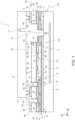
- FIG. 1 shows a MEMS pressure transducer 1 of capacitive type, hereinafter referred to as the MEMS transducer 1, and an orthogonal reference system XYZ.
- the MEMS transducer 1 comprises a semiconductor body 2, which is upwardly delimited by a front surface S 2 , parallel to the plane XY.
- a buried cavity 3 extends inside the semiconductor body 2, at a distance from the front surface S 2 .
- a lower portion of a trench 11 extends through part of the semiconductor body 2, starting from the front surface S 2 , so as to communicate downwardly with the buried cavity 3 and laterally delimit a portion 9' of the semiconductor body 2, which delimits the buried cavity 3 upwardly, and which is hereinafter referred to as the suspended portion 9' of the semiconductor body 2.
- the suspended portion 9' of the semiconductor body 2 extends cantilever, above the buried cavity 3, starting from a fixed portion 9" of the semiconductor body 2.
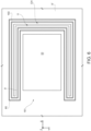
- the trench 11 may have a 'C' shape, in top-view, as shown in Figure 2 , wherein the trench 11 is shown in a simplified manner with respect to what has been shown in Figure 1 .
- the MEMS transducer 1 further comprises a lower dielectric region 4, which extends above the front surface S 2 , in direct contact with the semiconductor body 2, and is formed, for example, by thermal oxide.
- a lower dielectric region 4 covers the fixed portion 9" of the semiconductor body 2.
- part of the lower dielectric region 4 extends over the suspended portion 9' of the semiconductor body 2.
- the MEMS transducer 1 further comprises a stopping region 6, which extends on the lower dielectric region 4 and may be formed, for example, by aluminum oxide (Al 2 O 3 ).
- part of the stopping region 6 partially covers the part of the lower dielectric region 4 which covers the fixed portion 9" of the semiconductor body 2. Furthermore, part of the stopping region 6 extends on the part of the lower dielectric region 4 that overlies the suspended portion 9' of the semiconductor body 2. In addition, and without any loss of generality, the stopping region 6 does not entirely cover the lower dielectric region 4, but leaves exposed a part of the lower dielectric region 4.
- the MEMS transducer 1 further comprises a lower conductive structure 8 of polysilicon, which comprises a routing region 10, which, without any loss of generality, extends on a portion of the stopping region 6 that overlies, at a distance, the fixed portion 9" of the semiconductor body 2.
- the lower conductive structure 8 further comprises a lower electrode region 12, a lower anchoring region 14 and a covering region 16, which are therefore formed by polysilicon, extend on the part of the stopping region 6 which overlies, at a distance, the suspended portion 9' of the semiconductor body 2 and are coplanar with each other and with the routing region 10. Furthermore, the lower electrode region 12, the lower anchoring region 14 and the covering region 16 are laterally separated from each other. Furthermore, the lower conductive structure 8 comprises a pair of connection regions RC (visible in Figure 2 ).
- the lower conductive structure 8 also comprises a ground contact region 18, which extends on the part of the lower dielectric region 4 left exposed by the stopping region 6 and, without any loss of generality, is laterally offset with respect to the buried cavity 3; furthermore, the ground contact region 18 is separated from the routing region 10, the lower electrode region 12, the lower anchoring region 14, the covering region 16 and the connection regions RC and extends in part through the lower dielectric region 4, so as to contact, downwardly, the fixed portion 9" of the semiconductor body 2.
- the lower electrode region 12, the lower anchoring region 14, the covering region 16 and the connection regions RC overlie, at a distance, the buried cavity 3. Furthermore, as shown qualitatively in Figure 2 , wherein the lower electrode region 12 has been assumed to have an approximately circular shape in top-view, the covering region 16 has an approximately 'C' shape and laterally surrounds the lower electrode region 12; in particular, without any loss of generality, the covering region 16 surrounds the lower electrode region 12 entirely, except for a first opening A', which is precisely laterally delimited by the covering region 16.
- the lower anchoring region 14 has an elongated shape, approximately a 'C' shape (in top-view) and laterally surrounds the covering region 16.
- the lower anchoring region 14 surrounds the covering region 16 entirely, except for a second opening A", which is precisely laterally delimited by the lower anchoring region 14.
- both the first and the second openings A', A" are delimited downwardly by corresponding exposed portions of the stopping region 6.
- the lower conductive structure 8 further comprises a contact region 19 (visible in Figure 2 ), which is coplanar with the lower electrode region 12, the lower anchoring region 14, the covering region 16 and the connection regions RC.
- the contact region 19 extends through the first and the second openings A', A" and is interposed, in direct contact, between the lower electrode region 12 and the routing region 10 (not shown in Figure 2 ).
- the connection regions RC extend on opposite sides of a portion of the contact region 19, in a symmetrical manner and parallel to the axis Y, in such a way that each connection region RC has ends integral with the lower anchoring region 14 and the covering region 16, respectively. In this manner, the lower anchoring region 14, the covering region 16 and the connection regions RC form a single region, which laterally surrounds, at a distance, the lower electrode region 12.
- the MEMS transducer 1 further comprises an upper dielectric region 20, which is formed for example by TEOS oxide and extends above the routing region 10, the ground contact region 18, as well as above an outer portion of the lower anchoring region 14, described below.
- the upper dielectric region 20 also extends on the part of the lower dielectric region 4 left exposed by the stopping region 6 and on the portions of the stopping region 6 which extend into the space separating the outer portion of the lower anchoring region 14 from the routing region 10.
- an upper portion of the trench 11 extends through the part of the upper dielectric region 20 which extends on the part of the lower dielectric region 4 left exposed by the stopping region 6 and laterally offset with respect to the ground contact region 18.
- the MEMS transducer 1 further comprises a first, a second and a third upper conductive structure 30, 40, 50, which are formed by polysilicon and have approximately a same shape, in top-view.
- the first upper conductive structure 30 comprises a respective annular region 32, which in top-view has an annular shape and extends above portions of the upper dielectric region 20, in direct contact.
- the annular region 32 of the first upper conductive structure 30 extends above portions of the upper dielectric region 20 that overlie the routing region 10 and above portions of the upper dielectric region 20 that overlie the ground contact region 18.
- part of the annular region 32 traverses the upper dielectric region 20, so as to contact the ground contact region 18.
- the annular region 32 surrounds the trench 11, so as to overlie, at a distance, the fixed portion 9" of the semiconductor body 2.
- the first upper conductive structure 30 further comprises a respective peripheral region 34, which extends on a portion of the upper dielectric region 20 that overlies the routing region 10, outside the annular region 32; furthermore, the peripheral region 34 also extends through the upper dielectric region 20, so as to contact the underlying routing region 10.
- the first upper conductive structure 30 further comprises an inner region 36, hereinafter referred to as the first inner region 36.
- the first inner region 36 comprises a suspended portion 37' and an anchoring portion 37", which form a single monolithic polysilicon region.
- the anchoring portion 37" has an elongated shape, approximately a 'C' shape, in top-view; furthermore, the anchoring portion 37" is arranged above the lower anchoring region 14, wherewith it is in direct contact, and laterally delimits a cavity 39, hereinafter referred to as the sensing cavity 39.
- the anchoring portion 37" has a width (in the plane XY, along the perimeter of the respective elongated shape) that is smaller with respect to the width of the lower anchoring region 14 and is arranged with respect to the latter so as to leave exposed an inner portion of the lower anchoring region 14, which faces the sensing cavity 39, and furthermore so as to be laterally offset with respect to the aforementioned outer portion of the lower anchoring region 14, which, as mentioned, is overlaid by the upper dielectric region 20 (not shown in Figure 2 ).
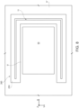
- the anchoring portion 37" is delimited by outer lateral walls P e (only one indicated in Figure 2 ) and by inner lateral walls Pi (only one indicated in Figure 2 ); the inner lateral walls Pi face the sensing cavity 39, while the outer lateral walls P e contact the upper dielectric region 20.
- the suspended portion 37' extends above the anchoring portion 37", so as to delimit the sensing cavity 39 upwardly, which is delimited downwardly by the inner portion of the lower anchoring region 14, the lower electrode region 12, the covering region 16, the connection regions RC, a part of the contact region 19 and portions of the stopping region 6 arranged below the suspended portion 37' and left exposed by the lower electrode region 12, the lower anchoring region 14, the covering region 16, the connection regions RC and the contact region 19.
- the suspended portion 37' is traversed by a plurality of holes 38 (two visible in Figure 1 ) of through type, which face the sensing cavity 39 downwardly. Furthermore, without any loss of generality, the suspended portion 37' extends laterally so as to protrude in part outside the anchoring portion 37", in top-view. The part of suspended portion 37' which protrudes externally with respect to the underlying anchoring portion 37" overlies a corresponding portion of the upper dielectric region 20, in direct contact.
- the suspended portion 37' is delimited downwardly by a flat surface S 37 , which, in rest conditions, is parallel to the plane XY; furthermore, the suspended portion 37' forms protection structures SX (optional), which depart from the flat surface S 37 in the direction of the lower conductive structure 8, for reasons which will be clarified below.
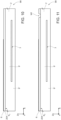
- the anchoring portion 37" laterally delimits a third opening A′′′, which is upwardly delimited by the suspended portion 37' and communicates downwardly with the second opening A", wherewith it forms a lateral opening A* of the sensing cavity 39.
- the lateral opening A* faces a corresponding portion of the upper dielectric region 20, which laterally closes the lateral opening A*, in such a way that the sensing cavity 39 is hermetically closed, with an internal pressure which may for example be comprised between 1 ⁇ bar and 1bar; furthermore, as visible in the example of Figure 4 , part of the upper dielectric region 20 may partially penetrate into the lateral opening A* of the sensing cavity 39, while not penetrating inside the sensing cavity 39.
- variants are possible (not shown) wherein the upper dielectric region 20 does not penetrate inside the lateral opening A*, while continuing to close it laterally.
- the second upper conductive structure 40 comprises a respective annular region 42, which overlies the annular region 32 of the first upper conductive structure 30, in direct contact.
- the annular region 42 may have approximately the same shape as the annular region 32.
- the second upper conductive structure 40 further comprises a respective peripheral portion 44, which extends above the peripheral portion 34 of the first upper conductive structure 30.
- the peripheral portion 44 may have approximately the same shape as the peripheral portion 34.
- the second upper conductive structure 40 also comprises a second inner region 46, which is layered and extends on the first inner region 36 and inside the holes 38, for example in a conformal manner, therefore without completely filling the holes 38, but coating the related lateral walls and the respective bottoms.
- the portions of the second inner region 46 which extend on the bottom of the holes 38 therefore face the sensing cavity 39.
- the third upper conductive structure 50 comprises a respective annular region 52, which overlies the annular region 42 of the second upper conductive structure 40, in direct contact.
- the annular region 52 may have approximately the same shape as the annular region 42.
- the third upper conductive structure 50 further comprises a respective peripheral portion 54, which extends on the peripheral portion 44 of the second upper conductive structure 40.
- the peripheral portion 54 may have approximately the same shape as the peripheral portion 44.
- the third upper conductive structure 50 further comprises a third inner region 56, which extends on the second inner region 46 and comprises portions which extend inside the holes 38, to fill them.
- a corresponding portion of the third inner region 56 is present, which is coated laterally and downwardly by a corresponding portion of the second inner region 46.
- the first, the second and the third inner regions 36, 46, 56 have approximately a same shape, in top-view. Furthermore, the part of the suspended portion 37' which overlies the sensing cavity 39 and the overlying portions of the second and the third inner regions 46, 56 form a membrane 55 of polysilicon, which has a thickness for example comprised between 1 ⁇ m and 6um, functions as the upper electrode of a variable detection capacitor and faces the underlying lower electrode region 12, which functions as a fixed lower electrode of the detection capacitor.
- the first, the second and the third inner regions 36, 46, 56 are formed by polysilicon, as a first approximation no lattice discontinuities occur between the first, the second and the third inner regions 36, 46, 56.
- first, the second and the third upper conductive structures 30, 40, 50 are patterned in such a way that the membrane 55 is laterally separated, by a trench 59, from the annular regions 32, 42, 52; hereinafter reference is made to the upper trench 59 to indicate the trench 59.
- peripheral portions 34, 44, 54 are separated from the annular regions 32, 42, 52 by an opening 61, which faces the upper dielectric region 20.
- the first, the second and the third upper conductive structures 30, 40, 50 form a conductive body 63, which forms, together with the semiconductor body 2, the lower dielectric region 4, the stopping region 6 and the lower conductive structure 8, a main body 65. Furthermore, the conductive body 63 is traversed by the opening 61 and by the upper trench 59; furthermore, a part of the upper trench 59 faces the upper dielectric region 20, while another part of the upper trench 59 faces the underlying upper portion of the trench 11, wherewith it is in fluidic communication.
- the MEMS transducer 1 further comprises a plurality of pads 66 of conductive material (for example, aluminum, copper or gold).
- pads 66 of conductive material for example, aluminum, copper or gold.
- a further pad is electrically connected to the lower anchoring region 14, so as to be set to the same potential as the membrane 55; in use, a voltage equal to the voltage present between the membrane 55 and the lower electrode region 12 is present between this pad and the pad 66.
- the MEMS transducer 1 further comprises a conductive coupling region 68, which is formed for example by metal material (for example, copper, aluminum or gold), has an annular shape and extends above the annular region 52 of the third upper conductive structure 50, in direct contact. Furthermore, although not visible in Figure 1 , the conductive coupling region 68 is electrically connected (for example) to the ground contact region 18, so as to be set to the same potential as the semiconductor body 2.
- a conductive coupling region 68 which is formed for example by metal material (for example, copper, aluminum or gold), has an annular shape and extends above the annular region 52 of the third upper conductive structure 50, in direct contact. Furthermore, although not visible in Figure 1 , the conductive coupling region 68 is electrically connected (for example) to the ground contact region 18, so as to be set to the same potential as the semiconductor body 2.
- the main body 6 also comprises a passivation region 69, which is formed for example by silicon nitride (SiN) or nitride oxide and extends over the upper conductive structure 50, in direct contact, leaving exposed the pads 66 and the conductive coupling region 68. Furthermore, optionally, the passivation region 69 may leave exposed the third inner region 56, so as to reduce the mechanical stresses to which the membrane 55 is subject.
- a passivation region 69 is formed for example by silicon nitride (SiN) or nitride oxide and extends over the upper conductive structure 50, in direct contact, leaving exposed the pads 66 and the conductive coupling region 68.
- the passivation region 69 may leave exposed the third inner region 56, so as to reduce the mechanical stresses to which the membrane 55 is subject.
- the passivation region 69 coats the lateral walls of the opening 61, as well as the lateral walls of the upper trench 59; in addition, the passivation region 69 coats the portions of the upper dielectric region 20 which form the bottom of the upper trench 59 and the lateral walls of the upper portion of the trench 11.
- the passivation region 69 coats upwardly the portions of the upper dielectric region 20 left exposed by the conductive body 63 and also laterally coats the portions of the lower dielectric region 4 and of the upper dielectric region 20 that face the trench 11, so as to form a protective structure which prevents any humidity present around the membrane 55 from penetrating inside the portions of the upper dielectric region 20 that surround the anchoring portion 37" and inside the portions of the lower dielectric region 4 that are arranged below the sensing cavity 39; in this manner it is avoided that, following the absorption of humidity by these portions of the lower dielectric region 4 and of the upper dielectric region 20, mechanical stresses are generated which entail an undesired deformation of the sensing cavity 39, which causes a drift of the response of the MEMS transducer 1.
- the first, the second and the third inner regions 36, 46, 56 extend above part of the dielectric support structure 100.
- the dielectric support structure 100 is laterally coated by the passivation region 69, except for the part of the dielectric support structure 100 which is integral with portions of the lower dielectric region 4 and of the upper dielectric region 20 which overlie the fixed portion 9" of the semiconductor body 2.
- the sensing cavity 39 extends inside the dielectric support structure 100.
- the passivation region 69 coats upwardly the portions of the dielectric support structure 100 left exposed by the first, the second and the third inner regions 36, 46, 56.
- the MEMS transducer 1 also comprises a cap 70 formed by semiconductor material, which is coupled to the conductive body 63 so as to form an accommodation chamber 75, having the membrane 55 extending therewithin.
- the sensing cavity 39 does not fluidically communicate with the accommodation chamber 75, i.e. it is fluidically insulated from the latter.
- the cap 70 is mechanically coupled to the conductive coupling region 68 by interposing a bonding region 72, which is formed, for example, by an aluminum and germanium (AlGe) alloy and is in fact interposed, in direct contact, between the conductive coupling region 68 and a corresponding portion of the cap 70.
- the cap 70 overlies the membrane 55 and the upper trench 59.
- the cap 70 is laterally offset with respect to the pads 66, to facilitate the formation of related electrical connections with an external circuitry (not shown).
- the accommodation chamber 75 comprises the upper trench 59 and communicates, thanks to the trench 11, with the buried cavity 3. Furthermore, the cap 70 is traversed by a respective hole 77, which places the accommodation chamber 75 in fluidic communication with the outside world.
- the accommodation chamber 75 and the buried cavity 3 are set to the same pressure present outside the MEMS transducer 1. Consequently, the membrane 55 is subject to a deformation which depends on the pressure difference present between the sensing cavity 39 and the outside world.
- the capacitance of the detection capacitor therefore varies as a function of the pressure present outside the MEMS transducer 1; therefore, a pressure capacitive transduction occurs.
- the capacitance variations, and therefore the value of the external pressure may be detected in a per se known manner on the basis of the electric voltage present between the membrane 55 and the lower electrode region 12. This detection may be performed by an external electronic circuit (not shown), which is coupled to the pads 66.
- the protection structures SX are for reducing the contact area between the membrane 55 and the set formed by the lower electrode region 12 and by the covering region 16, so as to avoid bonding phenomena in the case of excessive pressure. To this end, the protection structures SX are at the same potential as the lower anchoring region 14, the covering region 16 and the connection regions RC.
- the MEMS transducer 1 is characterized in that the shape of the membrane 55 (and therefore of the upper electrode of the detection capacitor) is defined by the anchoring portion 37", except for the possible uncertainty as to the extent of the penetration of the upper dielectric region 20 into the lateral opening A*.
- the dimensions of the membrane are defined by controlling the parameters of an etching process, in the present case the dimensions of the membrane 55 are more controllable, which results in an improvement in the accuracy of the pressure detection.
- the anchoring portion 37" of the first inner region 36 contacts with the underlying lower anchoring region 14 (therefore, they are at the same potential), only the lower electrode region 12 causes a fixed capacitance contribution, having an effective increase in the sensitivity value of the MEMS transducer 1 not corresponding thereto.
- the membrane 55 has no dielectric portions, which would entail the presence, inside the membrane 55, of regions having coefficients of thermal expansion that are very different from each other, resulting in the generation of unwanted mechanical stresses.
- the buried cavity 3 As to the buried cavity 3, it allows the mechanical stress induced by the package (not shown) of the MEMS transducer 1 on the fixed portion 9" of the semiconductor body 2 to be decoupled from the membrane 55 and from the suspended portion 9', in such a way that, as a first approximation, this mechanical stress does not affect the pressure measurement.
- the presence of the buried cavity 3 is optional; embodiments (not shown) are therefore possible wherein the buried cavity 3 and the lower portion of the trench 11 are absent.
- FIG 5 shows an embodiment which differs from what has been shown in Figure 1 for the following reasons.
- the lower conductive structure 8 comprises a lower barrier structure 80, which is formed by polysilicon and extends in part on the part of the lower dielectric region 4 left exposed by the stopping region 6 and in part through the lower dielectric region 4, so as to contact, downwardly, the suspended portion 9" of the semiconductor body 2. Furthermore, without any loss of generality, the lower barrier structure 80 is separated from the lower anchoring region 14 and from the ground contact region 18.
- the lower barrier structure 80 has a closed elongated shape (therefore, in top-view forms a ring-shaped region) and extends so as to laterally surround, at a distance, the upper portion of the trench 11. Consequently, in top-view, the upper portion of the trench 11 extends inside the lower barrier structure 80.
- the first, the second and the third upper conductive structures 30, 40, 50 comprise respective barrier regions, indicated by 130, 140, 150 respectively, which are formed by polysilicon and form an upper barrier structure 160.
- the barrier regions 130, 140, 150 have a same shape in top-view.
- the barrier region 130 of the first upper conductive structure 30 extends in part on the upper dielectric region 20 and in part through the upper dielectric region 20, so as to contact the underlying lower barrier structure 80.
- the barrier region 140 of the second upper conductive structure 140 overlies the barrier region 130 of the first upper conductive structure 30; the barrier region 150 of the third upper conductive structure 50 overlies the barrier region 140 of the second upper conductive structure 140.
- the upper barrier structure 160 is laterally offset with respect to the first, the second and the third inner regions 36, 46, 56 and overlies, in direct contact, the lower barrier structure 80. Furthermore, as visible in Figure 6 , the upper barrier structure 160 has a closed elongated shape, therefore in top-view it has a ring shape, and laterally delimits a channel CH, which in top-view is arranged inside the upper barrier structure 160 and overlies the underlying upper portion of the trench 11, wherewith it communicates. Furthermore, as still visible in Figure 6 , the first, the second and the third inner regions 36, 46, 56 are arranged outside the upper barrier structure 160, which extends in part above the suspended portion 9' of the semiconductor body 2 and in part above the fixed portion 9" of the semiconductor body 2.
- the passivation region 69 coats the upper barrier structure 160 laterally and upwardly, therefore it laterally coats the walls of the channel CH and the portion of upper dielectric region 20 left exposed by the first, the second and the third inner regions 36, 46, 56 and the barrier structure 160.
- the passivation region 69 does not penetrate inside the trench 11, to the advantage of the constructive simplicity of the MEMS transducer 1.
- the upper barrier structure 160 and the lower barrier structure 80 form a barrier which is impenetrable by humidity and laterally delimits an accommodation space 161, having the membrane 55 and the sensing cavity 39 extending therewithin.
- the lower barrier structure 80 and the barrier region 130 laterally surround a portion of the dielectric support structure 100 which surrounds the sensing cavity 39 laterally and downwardly. More particularly, the first, the second and the third inner regions 36, 46, 56 extend above part of this portion of the dielectric support structure 100, having the sensing cavity 39 extending therewithin. Even more particularly, this portion of the dielectric support structure 100 is surrounded by the lower barrier structure 80 and the barrier region 130, except for a respective part which is integral with portions of the lower dielectric region 4 and of the upper dielectric region 20 that overlie the fixed portion 9" of the semiconductor body 2.
- the parts of this portion of the dielectric support structure 100 left exposed by the first, the second and the third inner regions 36, 46, 56 and by the upper barrier structure 160 are coated upwardly by the passivation region 69.
- the upper barrier structure 160 is laterally spaced from the membrane 55, improving the protection of the latter against humidity.
- Figure 7 shows a further variant, which differs from what has been shown in Figure 5 for the following reasons.
- the upper barrier structure (here indicated by 260) is again formed by the barrier regions (respectively indicated by 230, 240, 250) of the first, the second and the third upper conductive structures 30, 40, 50 and is laterally spaced from the first, the second and the third inner regions 36, 46, 56; furthermore, the upper barrier structure 260 extends in part on the upper dielectric region 20 and in part through the upper dielectric region 20 and the lower dielectric region 4, so that the barrier region 230 contacts the front surface S 2 .
- the lower barrier structure 80 is absent.
- the upper portion of the trench 11 extends through the barrier regions 230, 240, 250 of the first, the second and the third upper conductive structures 30, 40, 50, while the lower portion of the trench 11 still extends through part of the semiconductor body 2.
- the trench 11 still has a 'C' shape, in top-view; furthermore, the upper portion of the trench 11 is entirely delimited, laterally, by the upper barrier structure 260, which, without any loss of generality, is laterally coated by the passivation region 69.
- the passivation region 69 leaves exposed a portion of the barrier region 250 of the third upper conductive structure 50 traversed by the trench 11.
- the aforementioned exposed portion of the barrier region 250 delimits a recess 251 which extends, starting from the upper conductive surface S 55 , downwards, where it communicates with the underlying trench 11.
- the MEMS transducer 1 is characterized by a certain constructive simplicity, in particular as to the trench 11, which may be formed by performing a single etch.
- the upper barrier structure 260 extends downwardly up to contacting the semiconductor body 2, and also laterally surrounds part of the dielectric support structure 100, it functions as a barrier against humidity, together with the portions of the passivation region 69 which coat the portions of the dielectric support structure 100 left exposed by the first, the second and the third inner regions 36, 46, 56 and the upper barrier structure 260.
- Figure 9 shows a further variant, which differs from what has been shown in Figure 7 for the following reasons.
- the lower barrier structure (here indicated by 380) is present and extends in part on the part of the lower dielectric region 4 left exposed by the stopping region 6 and in part through the lower dielectric region 4, so as to contact, downwardly, the semiconductor body 2.
- the upper barrier structure (here indicated by 360) is again formed by the barrier regions (respectively indicated by 330, 340, 350) of the first, the second and the third upper conductive structures 30, 40, 50.
- the barrier region 330 of the first upper conductive structure 30 extends in part on the upper dielectric region 20 and in part through the upper dielectric region 20, so as to contact the underlying lower barrier structure 380.
- the barrier region 350 of the third upper conductive structure 50 faces the upper membrane surface S 55 . Furthermore, the upper portion of the trench 11 extends, starting from the upper membrane surface S 55 , through the upper barrier structure 360 and through the lower barrier structure 380.
- FIG 9 is characterized, with respect to what has been shown in Figure 7 , in that the upper barrier structure 360 may be manufactured in a further simplified manner, since the lithographic mask used to form the trench 11 may be arranged at the same height as the upper membrane surface S 55 , thanks to the absence of the recess 251.
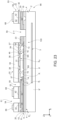
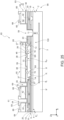
- Steps of a manufacturing process of the MEMS transducer 1 shown in Figure 1 are described hereinbelow, starting from a first semiconductive wafer 99 comprising the semiconductor body 2, wherein, in a per se known manner, the buried cavity 3 has been formed, as shown in Figure 10 .
- a lower dielectric layer 204 which is formed by thermal oxide and is intended to form the lower dielectric region 4, is present on the front surface S 2 of the semiconductor body 2.
- the stopping region 6 is arranged on a portion of the lower dielectric layer 204.
- the lower conductive structure 8 is formed, for example by performing a Low Pressure Chemical Vapor Deposition (LPCVD) of a polysilicon layer having a thickness comprised, for example, between 300nm and 1000nm and a successive etch.
- LPCVD Low Pressure Chemical Vapor Deposition
- a filling region 400 of oxide is formed on the portions of the stopping region 6 and the lower dielectric layer 204 left exposed by the lower conductive structure 8.
- a Plasma Enhanced Chemical Vapor Deposition (PECVD) of TEOS oxide may be performed, possibly followed by a planarization step.
- an intermediate dielectric layer 402 of TEOS oxide is formed with a thickness for example comprised between 250nm and 500nm, for example by LPCVD or PECVD deposition; furthermore, portions of the intermediate dielectric layer 402 are selectively removed, so as to form second process openings W2, which face the covering region 16.
- an upper dielectric layer 404 of TEOS oxide with a thickness for example comprised between 250nm and 500nm is formed on the intermediate dielectric layer 402, for example by LPCVD or PECVD deposition.
- the upper dielectric layer 404 fills the second process openings W2; consequently, the upper dielectric layer 404 has third process openings W3.
- the filling region 400, the intermediate dielectric layer 402 and the upper dielectric layer 404 are formed by a same material and form a single dielectric region, which is referred to as the front dielectric layer 420 (shown in Figure 16 ); therefore, the sole front dielectric layer 420 will be indicated in the following Figures.
- the front dielectric layer 420 is intended to form the upper dielectric region 20.
- portions of the front dielectric layer 420 are selectively removed (for example, by dry etch), so as to form a main anchoring window WA1 and a secondary anchoring window WA2, which traverse the front dielectric layer 420 and face the lower anchoring region 14 and the routing region 10, respectively.
- a polysilicon layer referred to as the first conductive layer 430, is formed on the front dielectric layer 420.
- the first conductive layer 430 is formed by LPCVD deposition, has a thickness comprised between 200nm and 500nm and is impermeable to gases.
- the first conductive layer 430 fills the main anchoring window WA1 and the secondary anchoring window WA2.
- the first conductive layer 430 fills the third process openings W3; the portions of the first conductive layer 430 which fill the third process openings W3 form the protection structures SX.
- the sacrificial region 420' to indicate the portion of the front dielectric layer 420 which is laterally delimited by the portion of the first conductive layer 430 which extends into the main anchoring window WA1, which is intended to form the anchoring portion 37" of the first inner region 36.
- the sacrificial region 420' overlies the lower electrode region 12, the covering region 16, the inner portion of the lower anchoring region 14 and the connection regions RC (not visible in Figure 17 ) .
- portions of the first conductive layer 430 are selectively removed, so as to form the holes 38, which face the sacrificial region 420'.
- a dry etch is for example performed.
- a second conductive layer 440 of polysilicon permeable to gases, is deposited on the first conductive layer 430.
- the second conductive layer 440 has a thickness comprised for example between 100nm and 300nm (for example, approximately equal to 120nm) .
- the second conductive layer 440 coats the lateral walls and the bottom of the holes 38 in a conformal manner, i.e. without filling them.
- the portions of sacrificial region 420' which form the bottoms of the holes 38 are then coated with corresponding portions of the second conductive layer 440, in direct contact.
- gaseous hydrofluoric acid HF
- second conductive layer 440 which coat the bottoms of the holes 38.
- the sacrificial region 420' is removed.
- the sensing cavity 39 is thus formed.
- a third conductive layer 450 of polysilicon, impermeable to gases, is formed on the second conductive layer 440.
- the third conductive layer 450 fills the holes 38, so as to hermetically close them, i.e. so as to prevent the gas from flowing through the holes 38.
- the third conductive layer 450 may be formed by performing an epitaxial growth of polysilicon (for example, at ambient pressure).
- an annealing may be performed in a nitrogen environment, to create a vacuum in the sensing cavity 39 or in any case to set the pressure value in the sensing cavity 39.
- portions of the first, the second and the third conductive layers 430, 440, 450 are selectively removed, for example by performing a dry etch, in such a way that the remaining portions of the first, the second and the third conductive layers 430, 440, 450 form the first, the second and the third upper conductive structures 30, 40, 50, respectively.
- the pads 66 and the conductive coupling region 68 may be formed, for example by a deposition of metal material and a successive patterning; furthermore, as shown again in Figure 23 , portions of the front dielectric layer 420 and underlying portions of the lower dielectric layer 204 are selectively removed, for example by a dry etch, so as to form the upper portion of the trench 11, which exposes a portion of the front surface S 2 . The remaining portions of the lower dielectric layer 204 and the front dielectric layer 420 form the lower dielectric region 4 and the upper dielectric region 20, respectively.
- the passivation region 69 is formed, for example by a deposition of silicon nitride.
- the passivation region 69 may also coat the pads 66, the conductive coupling region 68 and the third inner region 56 of the membrane 55; successively, portions of the passivation region 69 are selectively removed, so as to expose the pads 66, the conductive coupling region 68 and the third inner region 56 of the membrane 55.
- the passivation region 69 coats the lateral walls and the bottom of the upper portion of the trench 11.
- a portion of the passivation region 69 which coats the bottom of the upper portion of the trench 11 is selectively removed, so as to expose an underlying portion of the semiconductor body 2; subsequently, as shown again in Figure 25 , a part of the exposed portion of the semiconductor body 2 is selectively removed, so as to form the bottom portion of the trench 11, which communicates with the buried cavity 3, and release the suspended portion 9' of the semiconductor body 2.
- the main body 65 is thus formed.
- the first wafer 99 is mechanically coupled to a second wafer 799 which forms the cap 70.
- the coupling occurs by the bonding region 72.
- the second wafer 799 comprises a semiconductive portion 800 which overlies, at a distance, the pads 66, which is successively removed (operation not shown), so as to form the MEMS transducer 1 shown in Figure 1 .
- the manufacturing process proceeds in a per se known manner, for example by performing dicing operations (not shown).
- variants of Figures 5 , 7 and 9 may be manufactured with the same manufacturing process previously described, in particular as to forming the membrane 55 and the sensing cavity 39, and with resulting variations relating to the patterning of the passivation region 69.
- the lower barrier structure 80 may be formed in the same manner as the ground contact region 18.
- the upper barrier structure 160 it is formed in the same manner described with reference to the first, the second and the third inner regions 36, 46, 56, and simultaneously therewith; consequently, forming the upper barrier structure 160 provides for forming a corresponding anchoring window through the front dielectric layer 420, which faces the lower barrier structure 80, before forming the first, the second and the third conductive layers 430, 440, 450.
- the upper barrier structure 260 shown in Figure 7 it may be formed, for example, by performing the operations of selectively removing portions of the front dielectric layer 420 and of underlying portions of the lower dielectric layer 204 shown in Figure 23 before forming the first, the second and the third conductive layers 430, 440, 450 and the patterning thereof.
- the upper barrier structure 360 may be formed, for example, by forming the lower barrier structure 380 in the same manner and simultaneously with the ground contact region 18; successively, the upper barrier structure 360 is formed in the same manner described with reference to the first, the second and the third inner regions 36, 46, 56, and simultaneously therewith. Consequently, forming the upper barrier structure 360 may provide for forming a corresponding anchoring window through the front dielectric layer 420, which faces the lower barrier structure 380, before forming the first, the second and the third conductive layers 430, 440, 450.
- the trench 11 is then formed by performing a single etch through the upper barrier structure 360 and the lower barrier structure 380.
- the lateral extension of the sensing cavity 39 substantially does not depend on the parameters of an etching process, little controllable, but is defined by the shape of the anchoring portion 37".
- the membrane 55 is formed by a same material and is free from dielectric regions, therefore it does not have sub-regions with coefficients of thermal expansion different from each other, resulting in reduction of undesired mechanical stresses inside the membrane 55.
- the variable capacitor formed by the membrane 55 and the lower electrode region 12 is substantially free from fixed-capacitance parasitic capacitors.
- the conductive coupling region 68 instead of contacting the annular region 52 of the third upper conductive structure 50, may extend on an insulating region (not shown; for example, of silicon nitride), which is interposed between the annular region 52 and the conductive coupling region 68. In this case, the conductive coupling region 68 is electrically decoupled from the ground contact region 18.
- the buried cavity 3 may be absent, in which case the trench 11 stops at the front surface S 2 of the semiconductor body 2, as shown in Figure 24 .
- the third upper conductive structure 50 may be formed by amorphous silicon, rather than polysilicon.
- the third conductive layer 450 shown in Figure 21 is formed for example by PECVD deposition of amorphous silicon.
- the stopping region 6 may be formed by a material other than aluminum oxide, such as for example silicon nitride.
- the manufacturing process it may comprise annealings not explicitly mentioned above.
- the order of some steps may vary with respect to what has been described.
- the first conductive layer 430 may be formed by epitaxial polysilicon.
- all the previously mentioned polysilicon regions may have arbitrary doping levels and types, for example obtained by corresponding implants.
- front dielectric layer 420 and of the protection structures SX may also occur in a different manner than what has been described with reference to Figures 13-15 .
- the front dielectric layer may be formed with a single deposition; subsequently, the third openings W3 may be formed by selectively etching the front dielectric layer.
Landscapes
- Engineering & Computer Science (AREA)
- Chemical & Material Sciences (AREA)
- Physics & Mathematics (AREA)
- General Physics & Mathematics (AREA)
- Analytical Chemistry (AREA)
- Microelectronics & Electronic Packaging (AREA)
- Manufacturing & Machinery (AREA)
- Computer Hardware Design (AREA)
- Combustion & Propulsion (AREA)
- Pressure Sensors (AREA)
Abstract
Description
- The present invention relates to a capacitive microelectromechanical (MEMS) pressure transducer and to the related manufacturing process.
- As is known, numerous MEMS pressure transducers of capacitive type are currently available, which provide for forming a capacitor including an electrode formed by a membrane, which delimits a cavity and deforms as a function of pressure; in this manner, pressure variations are transduced into capacitance variations, which may be detected electronically.
- For example,
US 8,344,466 describes a manufacturing process of a MEMS transducer, wherein the cavity is formed by forming openings which traverse the membrane and face a dielectric region, the successive closure of these openings being obtained through deposition of a porous silicon layer; successively, part of the dielectric region is removed by etch with a chemical agent flowing through the porous silicon layer, resulting in the formation of the cavity and release of the membrane, which is then completed by depositing a further polysilicon layer. - The solution according to
US 8,344,466 may be formed starting from a single wafer, however the area of the electrode formed by the membrane depends on the aforementioned chemical etch, therefore it is not very controllable. - The aim of the present invention is therefore to provide a capacitive MEMS pressure transducer which overcomes at least in part the drawbacks of the prior art.
- According to the present invention a capacitive MEMS pressure transducer and a manufacturing process are provided, as defined in the attached claims.
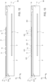
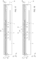
- For a better understanding of the present invention, embodiments thereof are now described, purely by way of nonlimiting example, with reference to the attached drawings, wherein:
-
Figure 1 schematically shows a cross-section of a MEMS transducer; -
Figure 2 schematically shows a top-view with portions removed of a part of the MEMS transducer shown inFigure 1 ; -
Figure 3 schematically shows a cross-section (taken along section line III-III shown inFigure 4 ) with portions removed of a part of the MEMS transducer shown inFigures 1 and2 ; -
Figure 4 schematically shows a top-view with portions removed of a part of the MEMS transducer shown inFigures 1 and2 ; -
Figure 5 schematically shows a cross-section of a variant of the MEMS transducer; -
Figure 6 schematically shows a top-view with portions removed of a part of the MEMS transducer shown inFigure 5 ; -
Figures 7 and9 schematically show cross-sections of variants of the MEMS transducer; -
Figure 8 schematically shows a top-view with portions removed of a part of the MEMS transducer shown inFigure 7 ; -
Figures 10-26 schematically show cross-sections of a MEMS transducer, during successive steps of a manufacturing process. -
Figure 1 shows a MEMS pressure transducer 1 of capacitive type, hereinafter referred to as the MEMS transducer 1, and an orthogonal reference system XYZ. - The MEMS transducer 1 comprises a
semiconductor body 2, which is upwardly delimited by a front surface S2, parallel to the plane XY. A buriedcavity 3 extends inside thesemiconductor body 2, at a distance from the front surface S2. Furthermore, a lower portion of atrench 11 extends through part of thesemiconductor body 2, starting from the front surface S2, so as to communicate downwardly with the buriedcavity 3 and laterally delimit a portion 9' of thesemiconductor body 2, which delimits the buriedcavity 3 upwardly, and which is hereinafter referred to as the suspended portion 9' of thesemiconductor body 2. In greater detail, the suspended portion 9' of thesemiconductor body 2 extends cantilever, above the buriedcavity 3, starting from a fixedportion 9" of thesemiconductor body 2. - Purely by way of example, the
trench 11 may have a 'C' shape, in top-view, as shown inFigure 2 , wherein thetrench 11 is shown in a simplified manner with respect to what has been shown inFigure 1 . - The MEMS transducer 1 further comprises a lower
dielectric region 4, which extends above the front surface S2, in direct contact with thesemiconductor body 2, and is formed, for example, by thermal oxide. In particular, part of the lowerdielectric region 4 covers thefixed portion 9" of thesemiconductor body 2. Furthermore, part of the lowerdielectric region 4 extends over the suspended portion 9' of thesemiconductor body 2. - The MEMS transducer 1 further comprises a
stopping region 6, which extends on the lowerdielectric region 4 and may be formed, for example, by aluminum oxide (Al2O3). - In greater detail, part of the
stopping region 6 partially covers the part of the lowerdielectric region 4 which covers thefixed portion 9" of thesemiconductor body 2. Furthermore, part of thestopping region 6 extends on the part of the lowerdielectric region 4 that overlies the suspended portion 9' of thesemiconductor body 2. In addition, and without any loss of generality, the stoppingregion 6 does not entirely cover the lowerdielectric region 4, but leaves exposed a part of the lowerdielectric region 4. - The MEMS transducer 1 further comprises a lower
conductive structure 8 of polysilicon, which comprises arouting region 10, which, without any loss of generality, extends on a portion of thestopping region 6 that overlies, at a distance, thefixed portion 9" of thesemiconductor body 2. - The lower
conductive structure 8 further comprises alower electrode region 12, alower anchoring region 14 and a coveringregion 16, which are therefore formed by polysilicon, extend on the part of thestopping region 6 which overlies, at a distance, the suspended portion 9' of thesemiconductor body 2 and are coplanar with each other and with therouting region 10. Furthermore, thelower electrode region 12, thelower anchoring region 14 and the coveringregion 16 are laterally separated from each other. Furthermore, the lowerconductive structure 8 comprises a pair of connection regions RC (visible inFigure 2 ). - The lower
conductive structure 8 also comprises aground contact region 18, which extends on the part of the lowerdielectric region 4 left exposed by thestopping region 6 and, without any loss of generality, is laterally offset with respect to the buriedcavity 3; furthermore, theground contact region 18 is separated from therouting region 10, thelower electrode region 12, thelower anchoring region 14, the coveringregion 16 and the connection regions RC and extends in part through the lowerdielectric region 4, so as to contact, downwardly, the fixedportion 9" of thesemiconductor body 2. - In greater detail, the
lower electrode region 12, thelower anchoring region 14, the coveringregion 16 and the connection regions RC overlie, at a distance, the buriedcavity 3. Furthermore, as shown qualitatively inFigure 2 , wherein thelower electrode region 12 has been assumed to have an approximately circular shape in top-view, the coveringregion 16 has an approximately 'C' shape and laterally surrounds thelower electrode region 12; in particular, without any loss of generality, the coveringregion 16 surrounds thelower electrode region 12 entirely, except for a first opening A', which is precisely laterally delimited by thecovering region 16. - Again without any loss of generality, the
lower anchoring region 14 has an elongated shape, approximately a 'C' shape (in top-view) and laterally surrounds the coveringregion 16. In particular, thelower anchoring region 14 surrounds the coveringregion 16 entirely, except for a second opening A", which is precisely laterally delimited by thelower anchoring region 14. Furthermore, both the first and the second openings A', A" are delimited downwardly by corresponding exposed portions of thestopping region 6. - The lower
conductive structure 8 further comprises a contact region 19 (visible inFigure 2 ), which is coplanar with thelower electrode region 12, thelower anchoring region 14, the coveringregion 16 and the connection regions RC. Thecontact region 19 extends through the first and the second openings A', A" and is interposed, in direct contact, between thelower electrode region 12 and the routing region 10 (not shown inFigure 2 ). Furthermore, purely by way of example, and without any loss of generality, the connection regions RC extend on opposite sides of a portion of thecontact region 19, in a symmetrical manner and parallel to the axis Y, in such a way that each connection region RC has ends integral with thelower anchoring region 14 and the coveringregion 16, respectively. In this manner, thelower anchoring region 14, the coveringregion 16 and the connection regions RC form a single region, which laterally surrounds, at a distance, thelower electrode region 12. - The MEMS transducer 1 further comprises an upper
dielectric region 20, which is formed for example by TEOS oxide and extends above therouting region 10, theground contact region 18, as well as above an outer portion of thelower anchoring region 14, described below. As qualitatively visible inFigure 1 , the upperdielectric region 20 also extends on the part of the lowerdielectric region 4 left exposed by thestopping region 6 and on the portions of thestopping region 6 which extend into the space separating the outer portion of thelower anchoring region 14 from therouting region 10. In this regard, an upper portion of thetrench 11 extends through the part of the upperdielectric region 20 which extends on the part of the lowerdielectric region 4 left exposed by thestopping region 6 and laterally offset with respect to theground contact region 18. - The MEMS transducer 1 further comprises a first, a second and a third upper
conductive structure - In detail, the first upper
conductive structure 30 comprises a respectiveannular region 32, which in top-view has an annular shape and extends above portions of the upperdielectric region 20, in direct contact. In particular, without any loss of generality, theannular region 32 of the first upperconductive structure 30 extends above portions of the upperdielectric region 20 that overlie therouting region 10 and above portions of the upperdielectric region 20 that overlie theground contact region 18. Although not shown, part of theannular region 32 traverses the upperdielectric region 20, so as to contact theground contact region 18. Also, although not shown, in top-view theannular region 32 surrounds thetrench 11, so as to overlie, at a distance, thefixed portion 9" of thesemiconductor body 2. - The first upper
conductive structure 30 further comprises a respectiveperipheral region 34, which extends on a portion of the upperdielectric region 20 that overlies therouting region 10, outside theannular region 32; furthermore, theperipheral region 34 also extends through the upperdielectric region 20, so as to contact theunderlying routing region 10. - The first upper
conductive structure 30 further comprises aninner region 36, hereinafter referred to as the firstinner region 36. - The first
inner region 36 comprises a suspended portion 37' and ananchoring portion 37", which form a single monolithic polysilicon region. - In particular, as visible in
Figure 2 (wherein the position of the perimeter of the suspended portion 37' is shown schematically in dotted lines), theanchoring portion 37" has an elongated shape, approximately a 'C' shape, in top-view; furthermore, theanchoring portion 37" is arranged above thelower anchoring region 14, wherewith it is in direct contact, and laterally delimits acavity 39, hereinafter referred to as thesensing cavity 39. - In greater detail, in top-view, the
anchoring portion 37" has a width (in the plane XY, along the perimeter of the respective elongated shape) that is smaller with respect to the width of thelower anchoring region 14 and is arranged with respect to the latter so as to leave exposed an inner portion of thelower anchoring region 14, which faces thesensing cavity 39, and furthermore so as to be laterally offset with respect to the aforementioned outer portion of thelower anchoring region 14, which, as mentioned, is overlaid by the upper dielectric region 20 (not shown inFigure 2 ). - In practice, the anchoring
portion 37" is delimited by outer lateral walls Pe (only one indicated inFigure 2 ) and by inner lateral walls Pi (only one indicated inFigure 2 ); the inner lateral walls Pi face thesensing cavity 39, while the outer lateral walls Pe contact the upperdielectric region 20. - The suspended portion 37' extends above the
anchoring portion 37", so as to delimit thesensing cavity 39 upwardly, which is delimited downwardly by the inner portion of thelower anchoring region 14, thelower electrode region 12, the coveringregion 16, the connection regions RC, a part of thecontact region 19 and portions of thestopping region 6 arranged below the suspended portion 37' and left exposed by thelower electrode region 12, thelower anchoring region 14, the coveringregion 16, the connection regions RC and thecontact region 19. - The suspended portion 37' is traversed by a plurality of holes 38 (two visible in
Figure 1 ) of through type, which face thesensing cavity 39 downwardly. Furthermore, without any loss of generality, the suspended portion 37' extends laterally so as to protrude in part outside the anchoringportion 37", in top-view. The part of suspended portion 37' which protrudes externally with respect to theunderlying anchoring portion 37" overlies a corresponding portion of the upperdielectric region 20, in direct contact. - Again without any loss of generality, in the example shown in
Figure 1 , the suspended portion 37' is delimited downwardly by a flat surface S37, which, in rest conditions, is parallel to the plane XY; furthermore, the suspended portion 37' forms protection structures SX (optional), which depart from the flat surface S37 in the direction of the lowerconductive structure 8, for reasons which will be clarified below. - In greater detail, as also visible in
Figure 3 , the anchoringportion 37" laterally delimits a third opening A‴, which is upwardly delimited by the suspended portion 37' and communicates downwardly with the second opening A", wherewith it forms a lateral opening A* of thesensing cavity 39. The lateral opening A* faces a corresponding portion of the upperdielectric region 20, which laterally closes the lateral opening A*, in such a way that thesensing cavity 39 is hermetically closed, with an internal pressure which may for example be comprised between 1µbar and 1bar; furthermore, as visible in the example ofFigure 4 , part of the upperdielectric region 20 may partially penetrate into the lateral opening A* of thesensing cavity 39, while not penetrating inside thesensing cavity 39. However, variants are possible (not shown) wherein the upperdielectric region 20 does not penetrate inside the lateral opening A*, while continuing to close it laterally. - The second upper
conductive structure 40 comprises a respectiveannular region 42, which overlies theannular region 32 of the first upperconductive structure 30, in direct contact. In top-view, theannular region 42 may have approximately the same shape as theannular region 32. - The second upper
conductive structure 40 further comprises a respectiveperipheral portion 44, which extends above theperipheral portion 34 of the first upperconductive structure 30. In top-view, theperipheral portion 44 may have approximately the same shape as theperipheral portion 34. - The second upper
conductive structure 40 also comprises a secondinner region 46, which is layered and extends on the firstinner region 36 and inside theholes 38, for example in a conformal manner, therefore without completely filling theholes 38, but coating the related lateral walls and the respective bottoms. The portions of the secondinner region 46 which extend on the bottom of theholes 38 therefore face thesensing cavity 39. - The third upper
conductive structure 50 comprises a respectiveannular region 52, which overlies theannular region 42 of the second upperconductive structure 40, in direct contact. In top-view, theannular region 52 may have approximately the same shape as theannular region 42. - The third upper
conductive structure 50 further comprises a respectiveperipheral portion 54, which extends on theperipheral portion 44 of the second upperconductive structure 40. In top-view, theperipheral portion 54 may have approximately the same shape as theperipheral portion 44. - The third upper
conductive structure 50 further comprises a thirdinner region 56, which extends on the secondinner region 46 and comprises portions which extend inside theholes 38, to fill them. In other words, in each hole 38 a corresponding portion of the thirdinner region 56 is present, which is coated laterally and downwardly by a corresponding portion of the secondinner region 46. - As mentioned, the first, the second and the third
inner regions sensing cavity 39 and the overlying portions of the second and the thirdinner regions membrane 55 of polysilicon, which has a thickness for example comprised between 1µm and 6um, functions as the upper electrode of a variable detection capacitor and faces the underlyinglower electrode region 12, which functions as a fixed lower electrode of the detection capacitor. Furthermore, since, while being manufactured, as described below, at different times, the first, the second and the thirdinner regions inner regions - In addition, the first, the second and the third upper
conductive structures membrane 55 is laterally separated, by atrench 59, from theannular regions upper trench 59 to indicate thetrench 59. Furthermore, theperipheral portions annular regions opening 61, which faces the upperdielectric region 20. - In practice, the first, the second and the third upper
conductive structures conductive body 63, which forms, together with thesemiconductor body 2, the lowerdielectric region 4, the stoppingregion 6 and the lowerconductive structure 8, amain body 65. Furthermore, theconductive body 63 is traversed by theopening 61 and by theupper trench 59; furthermore, a part of theupper trench 59 faces the upperdielectric region 20, while another part of theupper trench 59 faces the underlying upper portion of thetrench 11, wherewith it is in fluidic communication. - The MEMS transducer 1 further comprises a plurality of
pads 66 of conductive material (for example, aluminum, copper or gold). InFigure 1 only onepad 66 is visible, which overlies theperipheral portion 54 of the third upperconductive structure 50, in direct contact; thereby, thepad 66 is in electrical contact with therouting region 10, and therefore also with thelower electrode region 12. In use, thepad 66 is therefore set to the same potential as thelower electrode region 12. Although not shown, and purely by way of example, a further pad is electrically connected to thelower anchoring region 14, so as to be set to the same potential as themembrane 55; in use, a voltage equal to the voltage present between themembrane 55 and thelower electrode region 12 is present between this pad and thepad 66. - The MEMS transducer 1 further comprises a
conductive coupling region 68, which is formed for example by metal material (for example, copper, aluminum or gold), has an annular shape and extends above theannular region 52 of the third upperconductive structure 50, in direct contact. Furthermore, although not visible inFigure 1 , theconductive coupling region 68 is electrically connected (for example) to theground contact region 18, so as to be set to the same potential as thesemiconductor body 2. - The
main body 6 also comprises apassivation region 69, which is formed for example by silicon nitride (SiN) or nitride oxide and extends over the upperconductive structure 50, in direct contact, leaving exposed thepads 66 and theconductive coupling region 68. Furthermore, optionally, thepassivation region 69 may leave exposed the thirdinner region 56, so as to reduce the mechanical stresses to which themembrane 55 is subject. - In addition, in the example shown in
Figure 1 , thepassivation region 69 coats the lateral walls of theopening 61, as well as the lateral walls of theupper trench 59; in addition, thepassivation region 69 coats the portions of the upperdielectric region 20 which form the bottom of theupper trench 59 and the lateral walls of the upper portion of thetrench 11. - In greater detail, the
passivation region 69 coats upwardly the portions of the upperdielectric region 20 left exposed by theconductive body 63 and also laterally coats the portions of the lowerdielectric region 4 and of the upperdielectric region 20 that face thetrench 11, so as to form a protective structure which prevents any humidity present around themembrane 55 from penetrating inside the portions of the upperdielectric region 20 that surround the anchoringportion 37" and inside the portions of the lowerdielectric region 4 that are arranged below thesensing cavity 39; in this manner it is avoided that, following the absorption of humidity by these portions of the lowerdielectric region 4 and of the upperdielectric region 20, mechanical stresses are generated which entail an undesired deformation of thesensing cavity 39, which causes a drift of the response of the MEMS transducer 1. - In other words, referring to the
dielectric support structure 100 to indicate the portions of the lowerdielectric region 4 and of the upperdielectric region 20 laterally delimited by the upper portion of thetrench 11 and arranged above the suspended portion 9' of thesemiconductor body 2, the first, the second and the thirdinner regions dielectric support structure 100. Thedielectric support structure 100 is laterally coated by thepassivation region 69, except for the part of thedielectric support structure 100 which is integral with portions of the lowerdielectric region 4 and of the upperdielectric region 20 which overlie the fixedportion 9" of thesemiconductor body 2. Thesensing cavity 39 extends inside thedielectric support structure 100. Furthermore, thepassivation region 69 coats upwardly the portions of thedielectric support structure 100 left exposed by the first, the second and the thirdinner regions - The MEMS transducer 1 also comprises a
cap 70 formed by semiconductor material, which is coupled to theconductive body 63 so as to form anaccommodation chamber 75, having themembrane 55 extending therewithin. Thesensing cavity 39 does not fluidically communicate with theaccommodation chamber 75, i.e. it is fluidically insulated from the latter. - In detail, the
cap 70 is mechanically coupled to theconductive coupling region 68 by interposing abonding region 72, which is formed, for example, by an aluminum and germanium (AlGe) alloy and is in fact interposed, in direct contact, between theconductive coupling region 68 and a corresponding portion of thecap 70. In particular, thecap 70 overlies themembrane 55 and theupper trench 59. Instead, without any loss of generality, thecap 70 is laterally offset with respect to thepads 66, to facilitate the formation of related electrical connections with an external circuitry (not shown). - In greater detail, the
accommodation chamber 75 comprises theupper trench 59 and communicates, thanks to thetrench 11, with the buriedcavity 3. Furthermore, thecap 70 is traversed by arespective hole 77, which places theaccommodation chamber 75 in fluidic communication with the outside world. - In use, the
accommodation chamber 75 and the buriedcavity 3 are set to the same pressure present outside the MEMS transducer 1. Consequently, themembrane 55 is subject to a deformation which depends on the pressure difference present between thesensing cavity 39 and the outside world. The capacitance of the detection capacitor therefore varies as a function of the pressure present outside the MEMS transducer 1; therefore, a pressure capacitive transduction occurs. In particular, the capacitance variations, and therefore the value of the external pressure, may be detected in a per se known manner on the basis of the electric voltage present between themembrane 55 and thelower electrode region 12. This detection may be performed by an external electronic circuit (not shown), which is coupled to thepads 66. Furthermore, the protection structures SX are for reducing the contact area between themembrane 55 and the set formed by thelower electrode region 12 and by thecovering region 16, so as to avoid bonding phenomena in the case of excessive pressure. To this end, the protection structures SX are at the same potential as thelower anchoring region 14, thecovering region 16 and the connection regions RC. - This having been said, the MEMS transducer 1 is characterized in that the shape of the membrane 55 (and therefore of the upper electrode of the detection capacitor) is defined by the anchoring
portion 37", except for the possible uncertainty as to the extent of the penetration of the upperdielectric region 20 into the lateral opening A*. In other words, unlike what occurs in the prior art, wherein the dimensions of the membrane are defined by controlling the parameters of an etching process, in the present case the dimensions of themembrane 55 are more controllable, which results in an improvement in the accuracy of the pressure detection. Furthermore, since the anchoringportion 37" of the firstinner region 36 contacts with the underlying lower anchoring region 14 (therefore, they are at the same potential), only thelower electrode region 12 causes a fixed capacitance contribution, having an effective increase in the sensitivity value of the MEMS transducer 1 not corresponding thereto. - As to the presence of the
covering region 16, it allows the area of the stoppingregion 6 left exposed to be reduced, resulting in the reduction of the probability that defectivenesses occur. Furthermore, themembrane 55 has no dielectric portions, which would entail the presence, inside themembrane 55, of regions having coefficients of thermal expansion that are very different from each other, resulting in the generation of unwanted mechanical stresses. - As to the buried
cavity 3, it allows the mechanical stress induced by the package (not shown) of the MEMS transducer 1 on the fixedportion 9" of thesemiconductor body 2 to be decoupled from themembrane 55 and from the suspended portion 9', in such a way that, as a first approximation, this mechanical stress does not affect the pressure measurement. In any case, the presence of the buriedcavity 3 is optional; embodiments (not shown) are therefore possible wherein the buriedcavity 3 and the lower portion of thetrench 11 are absent. -
Figure 5 shows an embodiment which differs from what has been shown inFigure 1 for the following reasons. - In detail, the lower
conductive structure 8 comprises alower barrier structure 80, which is formed by polysilicon and extends in part on the part of the lowerdielectric region 4 left exposed by the stoppingregion 6 and in part through the lowerdielectric region 4, so as to contact, downwardly, the suspendedportion 9" of thesemiconductor body 2. Furthermore, without any loss of generality, thelower barrier structure 80 is separated from thelower anchoring region 14 and from theground contact region 18. - In greater detail, as visible in
Figure 6 (wherein, for the sake of simplicity, inter alia, the lowerdielectric region 4 and the upperdielectric region 20 are not shown), thelower barrier structure 80 has a closed elongated shape (therefore, in top-view forms a ring-shaped region) and extends so as to laterally surround, at a distance, the upper portion of thetrench 11. Consequently, in top-view, the upper portion of thetrench 11 extends inside thelower barrier structure 80. - The first, the second and the third upper
conductive structures upper barrier structure 160. As a first approximation, thebarrier regions - In greater detail, the
barrier region 130 of the first upperconductive structure 30 extends in part on the upperdielectric region 20 and in part through the upperdielectric region 20, so as to contact the underlyinglower barrier structure 80. - The
barrier region 140 of the second upperconductive structure 140 overlies thebarrier region 130 of the first upperconductive structure 30; thebarrier region 150 of the third upperconductive structure 50 overlies thebarrier region 140 of the second upperconductive structure 140. - In practice, the
upper barrier structure 160 is laterally offset with respect to the first, the second and the thirdinner regions lower barrier structure 80. Furthermore, as visible inFigure 6 , theupper barrier structure 160 has a closed elongated shape, therefore in top-view it has a ring shape, and laterally delimits a channel CH, which in top-view is arranged inside theupper barrier structure 160 and overlies the underlying upper portion of thetrench 11, wherewith it communicates. Furthermore, as still visible inFigure 6 , the first, the second and the thirdinner regions upper barrier structure 160, which extends in part above the suspended portion 9' of thesemiconductor body 2 and in part above the fixedportion 9" of thesemiconductor body 2. Furthermore, thepassivation region 69 coats theupper barrier structure 160 laterally and upwardly, therefore it laterally coats the walls of the channel CH and the portion of upperdielectric region 20 left exposed by the first, the second and the thirdinner regions barrier structure 160. - The
passivation region 69 does not penetrate inside thetrench 11, to the advantage of the constructive simplicity of the MEMS transducer 1. In fact, theupper barrier structure 160 and thelower barrier structure 80 form a barrier which is impenetrable by humidity and laterally delimits anaccommodation space 161, having themembrane 55 and thesensing cavity 39 extending therewithin. - In particular, the
lower barrier structure 80 and thebarrier region 130 laterally surround a portion of thedielectric support structure 100 which surrounds thesensing cavity 39 laterally and downwardly. More particularly, the first, the second and the thirdinner regions dielectric support structure 100, having thesensing cavity 39 extending therewithin. Even more particularly, this portion of thedielectric support structure 100 is surrounded by thelower barrier structure 80 and thebarrier region 130, except for a respective part which is integral with portions of the lowerdielectric region 4 and of the upperdielectric region 20 that overlie the fixedportion 9" of thesemiconductor body 2. Furthermore, the parts of this portion of thedielectric support structure 100 left exposed by the first, the second and the thirdinner regions upper barrier structure 160 are coated upwardly by thepassivation region 69. In this manner, theupper barrier structure 160 is laterally spaced from themembrane 55, improving the protection of the latter against humidity. -
Figure 7 shows a further variant, which differs from what has been shown inFigure 5 for the following reasons. - In detail, the upper barrier structure (here indicated by 260) is again formed by the barrier regions (respectively indicated by 230, 240, 250) of the first, the second and the third upper
conductive structures inner regions upper barrier structure 260 extends in part on the upperdielectric region 20 and in part through the upperdielectric region 20 and the lowerdielectric region 4, so that thebarrier region 230 contacts the front surface S2. Thelower barrier structure 80 is absent. - The upper portion of the
trench 11 extends through thebarrier regions conductive structures trench 11 still extends through part of thesemiconductor body 2. - As shown qualitatively in
Figure 8 , thetrench 11 still has a 'C' shape, in top-view; furthermore, the upper portion of thetrench 11 is entirely delimited, laterally, by theupper barrier structure 260, which, without any loss of generality, is laterally coated by thepassivation region 69. - Again by way of example, the
passivation region 69 leaves exposed a portion of thebarrier region 250 of the third upperconductive structure 50 traversed by thetrench 11. Referring to the upper conductive surface S55 to indicate the upper surface of the thirdinner region 56 and of thebarrier region 250, the aforementioned exposed portion of thebarrier region 250 delimits arecess 251 which extends, starting from the upper conductive surface S55, downwards, where it communicates with theunderlying trench 11. - In practice, the MEMS transducer 1 is characterized by a certain constructive simplicity, in particular as to the
trench 11, which may be formed by performing a single etch. Furthermore, since theupper barrier structure 260 extends downwardly up to contacting thesemiconductor body 2, and also laterally surrounds part of thedielectric support structure 100, it functions as a barrier against humidity, together with the portions of thepassivation region 69 which coat the portions of thedielectric support structure 100 left exposed by the first, the second and the thirdinner regions upper barrier structure 260. -
Figure 9 shows a further variant, which differs from what has been shown inFigure 7 for the following reasons. - The lower barrier structure (here indicated by 380) is present and extends in part on the part of the lower
dielectric region 4 left exposed by the stoppingregion 6 and in part through the lowerdielectric region 4, so as to contact, downwardly, thesemiconductor body 2. The upper barrier structure (here indicated by 360) is again formed by the barrier regions (respectively indicated by 330, 340, 350) of the first, the second and the third upperconductive structures barrier region 330 of the first upperconductive structure 30 extends in part on the upperdielectric region 20 and in part through the upperdielectric region 20, so as to contact the underlyinglower barrier structure 380. - The
barrier region 350 of the third upperconductive structure 50 faces the upper membrane surface S55. Furthermore, the upper portion of thetrench 11 extends, starting from the upper membrane surface S55, through theupper barrier structure 360 and through thelower barrier structure 380. - The embodiment shown in
Figure 9 is characterized, with respect to what has been shown inFigure 7 , in that theupper barrier structure 360 may be manufactured in a further simplified manner, since the lithographic mask used to form thetrench 11 may be arranged at the same height as the upper membrane surface S55, thanks to the absence of therecess 251. - Steps of a manufacturing process of the MEMS transducer 1 shown in
Figure 1 are described hereinbelow, starting from a firstsemiconductive wafer 99 comprising thesemiconductor body 2, wherein, in a per se known manner, the buriedcavity 3 has been formed, as shown inFigure 10 . Furthermore, a lowerdielectric layer 204, which is formed by thermal oxide and is intended to form the lowerdielectric region 4, is present on the front surface S2 of thesemiconductor body 2. The stoppingregion 6 is arranged on a portion of the lowerdielectric layer 204. - This having been said, subsequently, as shown in
Figure 11 , a portion of the lowerdielectric layer 204 is removed, so as to form a first process opening W1, which faces the front surface S2 and is intended to be occupied by theground contact region 18. - Subsequently, as shown in
Figure 12 , the lowerconductive structure 8 is formed, for example by performing a Low Pressure Chemical Vapor Deposition (LPCVD) of a polysilicon layer having a thickness comprised, for example, between 300nm and 1000nm and a successive etch. - Successively, as shown in
Figure 13 , a fillingregion 400 of oxide is formed on the portions of the stoppingregion 6 and the lowerdielectric layer 204 left exposed by the lowerconductive structure 8. To this end, although not shown in detail, a Plasma Enhanced Chemical Vapor Deposition (PECVD) of TEOS oxide may be performed, possibly followed by a planarization step. - Subsequently, as shown in
Figure 14 , anintermediate dielectric layer 402 of TEOS oxide is formed with a thickness for example comprised between 250nm and 500nm, for example by LPCVD or PECVD deposition; furthermore, portions of theintermediate dielectric layer 402 are selectively removed, so as to form second process openings W2, which face thecovering region 16. - Successively, as shown in
Figure 15 , anupper dielectric layer 404 of TEOS oxide with a thickness for example comprised between 250nm and 500nm is formed on theintermediate dielectric layer 402, for example by LPCVD or PECVD deposition. Theupper dielectric layer 404 fills the second process openings W2; consequently, theupper dielectric layer 404 has third process openings W3. - In practice, the filling
region 400, theintermediate dielectric layer 402 and theupper dielectric layer 404 are formed by a same material and form a single dielectric region, which is referred to as the front dielectric layer 420 (shown inFigure 16 ); therefore, the sole frontdielectric layer 420 will be indicated in the following Figures. Thefront dielectric layer 420 is intended to form the upperdielectric region 20. - Subsequently, as shown in
Figure 16 , portions of thefront dielectric layer 420 are selectively removed (for example, by dry etch), so as to form a main anchoring window WA1 and a secondary anchoring window WA2, which traverse thefront dielectric layer 420 and face thelower anchoring region 14 and therouting region 10, respectively. - Subsequently, as shown in
Figure 17 , a polysilicon layer, referred to as the firstconductive layer 430, is formed on thefront dielectric layer 420. For example, the firstconductive layer 430 is formed by LPCVD deposition, has a thickness comprised between 200nm and 500nm and is impermeable to gases. The firstconductive layer 430 fills the main anchoring window WA1 and the secondary anchoring window WA2. Furthermore, the firstconductive layer 430 fills the third process openings W3; the portions of the firstconductive layer 430 which fill the third process openings W3 form the protection structures SX. - In the following, reference is made to the sacrificial region 420' to indicate the portion of the
front dielectric layer 420 which is laterally delimited by the portion of the firstconductive layer 430 which extends into the main anchoring window WA1, which is intended to form the anchoringportion 37" of the firstinner region 36. A portion of the firstconductive layer 430, which is intended to form the suspended portion 37' of the firstinner region 36, extends on the sacrificial region 420'. In addition, the sacrificial region 420' overlies thelower electrode region 12, thecovering region 16, the inner portion of thelower anchoring region 14 and the connection regions RC (not visible inFigure 17 ) . - Subsequently, as shown in
Figure 18 , portions of the firstconductive layer 430 are selectively removed, so as to form theholes 38, which face the sacrificial region 420'. To this end, a dry etch is for example performed. - Successively, as shown in
Figure 19 , a secondconductive layer 440, of polysilicon permeable to gases, is deposited on the firstconductive layer 430. The secondconductive layer 440 has a thickness comprised for example between 100nm and 300nm (for example, approximately equal to 120nm) . Furthermore, the secondconductive layer 440 coats the lateral walls and the bottom of theholes 38 in a conformal manner, i.e. without filling them. The portions of sacrificial region 420' which form the bottoms of theholes 38 are then coated with corresponding portions of the secondconductive layer 440, in direct contact. - Successively, as shown in
Figure 20 , gaseous hydrofluoric acid (HF) is flown through theholes 38, therefore through the portions of secondconductive layer 440 which coat the bottoms of theholes 38. In this manner, the sacrificial region 420' is removed. Thesensing cavity 39 is thus formed. - Subsequently, as shown in
Figure 21 , a thirdconductive layer 450 of polysilicon, impermeable to gases, is formed on the secondconductive layer 440. The thirdconductive layer 450 fills theholes 38, so as to hermetically close them, i.e. so as to prevent the gas from flowing through theholes 38. - In particular, in order to prevent the polysilicon from penetrating the
sensing cavity 39, creating unwanted contacts with thelower electrode region 12, the thirdconductive layer 450 may be formed by performing an epitaxial growth of polysilicon (for example, at ambient pressure). - Subsequently, although not shown, an annealing may be performed in a nitrogen environment, to create a vacuum in the
sensing cavity 39 or in any case to set the pressure value in thesensing cavity 39. - Successively, as shown in
Figure 22 , portions of the first, the second and the thirdconductive layers conductive layers conductive structures - Subsequently, as shown in
Figure 23 , thepads 66 and theconductive coupling region 68 may be formed, for example by a deposition of metal material and a successive patterning; furthermore, as shown again inFigure 23 , portions of thefront dielectric layer 420 and underlying portions of the lowerdielectric layer 204 are selectively removed, for example by a dry etch, so as to form the upper portion of thetrench 11, which exposes a portion of the front surface S2. The remaining portions of the lowerdielectric layer 204 and thefront dielectric layer 420 form the lowerdielectric region 4 and the upperdielectric region 20, respectively. - Subsequently, as shown in
Figure 24 , thepassivation region 69 is formed, for example by a deposition of silicon nitride. Although not shown in detail, initially thepassivation region 69 may also coat thepads 66, theconductive coupling region 68 and the thirdinner region 56 of themembrane 55; successively, portions of thepassivation region 69 are selectively removed, so as to expose thepads 66, theconductive coupling region 68 and the thirdinner region 56 of themembrane 55. Furthermore, as visible inFigure 24 , thepassivation region 69 coats the lateral walls and the bottom of the upper portion of thetrench 11. - Subsequently, as shown in
Figure 25 , a portion of thepassivation region 69 which coats the bottom of the upper portion of thetrench 11 is selectively removed, so as to expose an underlying portion of thesemiconductor body 2; subsequently, as shown again inFigure 25 , a part of the exposed portion of thesemiconductor body 2 is selectively removed, so as to form the bottom portion of thetrench 11, which communicates with the buriedcavity 3, and release the suspended portion 9' of thesemiconductor body 2. Themain body 65 is thus formed. - Subsequently, as shown in
Figure 26 , thefirst wafer 99 is mechanically coupled to asecond wafer 799 which forms thecap 70. In particular, the coupling occurs by thebonding region 72. Furthermore, thesecond wafer 799 comprises asemiconductive portion 800 which overlies, at a distance, thepads 66, which is successively removed (operation not shown), so as to form the MEMS transducer 1 shown inFigure 1 . Subsequently, the manufacturing process proceeds in a per se known manner, for example by performing dicing operations (not shown). - Although not shown in detail, the variants of
Figures 5 ,7 and9 may be manufactured with the same manufacturing process previously described, in particular as to forming themembrane 55 and thesensing cavity 39, and with resulting variations relating to the patterning of thepassivation region 69. - In greater detail, as to forming the lower barrier structure 80 (if any), it may be formed in the same manner as the
ground contact region 18. As to theupper barrier structure 160, it is formed in the same manner described with reference to the first, the second and the thirdinner regions upper barrier structure 160 provides for forming a corresponding anchoring window through thefront dielectric layer 420, which faces thelower barrier structure 80, before forming the first, the second and the thirdconductive layers - In the case of the
upper barrier structure 260 shown inFigure 7 , it may be formed, for example, by performing the operations of selectively removing portions of thefront dielectric layer 420 and of underlying portions of the lowerdielectric layer 204 shown inFigure 23 before forming the first, the second and the thirdconductive layers - In the case of the
upper barrier structure 360 shown inFigure 9 , it may be formed, for example, by forming thelower barrier structure 380 in the same manner and simultaneously with theground contact region 18; successively, theupper barrier structure 360 is formed in the same manner described with reference to the first, the second and the thirdinner regions upper barrier structure 360 may provide for forming a corresponding anchoring window through thefront dielectric layer 420, which faces thelower barrier structure 380, before forming the first, the second and the thirdconductive layers trench 11 is then formed by performing a single etch through theupper barrier structure 360 and thelower barrier structure 380. - The advantages which the present solution affords are clear from the preceding description.
- In particular, according to the present solution, the lateral extension of the
sensing cavity 39, and therefore also the shape of themembrane 55, substantially does not depend on the parameters of an etching process, little controllable, but is defined by the shape of the anchoringportion 37". Furthermore, themembrane 55 is formed by a same material and is free from dielectric regions, therefore it does not have sub-regions with coefficients of thermal expansion different from each other, resulting in reduction of undesired mechanical stresses inside themembrane 55. Furthermore, the variable capacitor formed by themembrane 55 and thelower electrode region 12 is substantially free from fixed-capacitance parasitic capacitors. - Finally, it is clear that modifications and variations may be made to the MEMS transducer and the related manufacturing process previously described and illustrated, without departing from the scope of the present invention, as defined in the attached claims.
- For example, the
conductive coupling region 68, instead of contacting theannular region 52 of the third upperconductive structure 50, may extend on an insulating region (not shown; for example, of silicon nitride), which is interposed between theannular region 52 and theconductive coupling region 68. In this case, theconductive coupling region 68 is electrically decoupled from theground contact region 18. - As previously mentioned, the buried
cavity 3 may be absent, in which case thetrench 11 stops at the front surface S2 of thesemiconductor body 2, as shown inFigure 24 . - The third upper
conductive structure 50 may be formed by amorphous silicon, rather than polysilicon. In this case, the thirdconductive layer 450 shown inFigure 21 is formed for example by PECVD deposition of amorphous silicon. - The stopping
region 6 may be formed by a material other than aluminum oxide, such as for example silicon nitride. - As to the manufacturing process, it may comprise annealings not explicitly mentioned above. The order of some steps may vary with respect to what has been described.
- For example, the first
conductive layer 430 may be formed by epitaxial polysilicon. - Furthermore, in general, all the previously mentioned polysilicon regions may have arbitrary doping levels and types, for example obtained by corresponding implants.
- The formation of the
front dielectric layer 420 and of the protection structures SX may also occur in a different manner than what has been described with reference toFigures 13-15 . For example, the front dielectric layer may be formed with a single deposition; subsequently, the third openings W3 may be formed by selectively etching the front dielectric layer.
Claims (19)
- A MEMS pressure transducer (1) comprising:- a semiconductor body (2);- a lower dielectric region (4,6), arranged above the semiconductor body (2);- a fixed electrode region (12) and a lower anchoring region (14), which are formed by conductive material, are arranged on the lower dielectric region (4,6) and are laterally separated from each other;- a membrane (55) of conductive material, which is suspended above the fixed electrode region (12), so as to delimit a cavity (39) upwardly, the fixed electrode region (12) facing the cavity, the membrane (55) being deformable as a function of pressure and forming a variable capacitor together with the fixed electrode region (12); and- an upper anchoring region (37") of conductive material, which laterally delimits the cavity (39) and is interposed, in direct contact, between the membrane (55) and the lower anchoring region (14);said transducer further comprising a first conductive region (36), which forms a part (37') of the membrane (55) and the upper anchoring region (37"); and wherein said part (37') of the membrane (55) is traversed by a number of holes (38) facing the cavity (39) and is impermeable to gases, with the exception of the holes (38); said transducer (1) further comprising:- a second conductive region (46), which is permeable to gases and extends on the first conductive region (36) and inside the holes (38), so as to face the cavity (39); and- a third conductive region (56), which is impermeable to gases and extends on the second conductive region (46);and wherein the second and the third conductive regions (46,56) form corresponding parts of the membrane (55).
- The transducer according to claim 1, wherein the third conductive region (56) is formed by polysilicon or amorphous silicon.
- The transducer according to claim 1 or 2, wherein the second conductive region (46) is formed by permeable polysilicon.
- The transducer according to any of the preceding claims, wherein the first conductive region (36) is formed by polysilicon.
- The transducer according to any of the preceding claims, wherein the upper anchoring region (37") laterally delimits a lateral opening (A*) of the cavity (39); said MEMS transducer (1) further comprising an upper dielectric region (20), which is arranged above the lower dielectric region (4,6) and laterally and externally surrounds the upper anchoring region (37"), so as to close the lateral opening (A*), said cavity (39) being hermetically closed.
- The transducer according to claim 5, wherein the lower dielectric region (4,6) and the upper dielectric region (20) form a dielectric support structure (100), said cavity (39) extending inside the dielectric support structure (100), the first, the second and the third conductive regions (36,46,56) overlying part of the dielectric support structure (100); said MEMS transducer (1) further comprising a passivation region (69) impermeable to humidity, which laterally coats part of the dielectric support structure (100) and coats upwardly portions of the dielectric support structure (100) left exposed by the first, the second and the third conductive regions (36,46,56).
- The transducer according to claim 5, wherein the lower dielectric region (4,6) and the upper dielectric region (20) form a dielectric support structure (100), said cavity (39) extending inside the dielectric support structure (100), the first, the second and the third conductive regions (36,46,56) overlying part of the dielectric support structure (100); said MEMS transducer (1) further comprising a lower barrier structure (80), which extends through the lower dielectric region (4,6) and contacts the semiconductor body (2), and an upper barrier structure (160), which is laterally spaced from the membrane (55) and extends in part above the upper dielectric region (20) and in part through the upper dielectric region (20), so as to contact the lower barrier structure (80), the lower barrier structure (80) and the upper barrier structure (160) being of conductive material, being impermeable to humidity and laterally surrounding part of the dielectric support structure (100); and wherein the upper barrier structure (160) and the first, the second and the third conductive regions (36,46,56) leave exposed portions of the dielectric support structure (100), the MEMS transducer (1) further comprising a passivation region (69) impermeable to humidity, which coats upwardly the portions of the dielectric support structure (100) left exposed by the upper barrier structure (160) and the first, the second and the third conductive regions (36,46,56).
- The transducer according to any of the preceding claims, wherein the semiconductor body (2) houses a buried cavity (3), which is upwardly delimited by a suspended portion (9') of the semiconductor body (2), which is laterally delimited by a trench (11) which traverses part of the semiconductor body (2) and communicates downwardly with the buried cavity (3), said suspended portion (9') extending cantilever from a fixed portion (9") of the semiconductor body (2); and wherein the cavity (39) is arranged above the suspended portion (9').
- The transducer according to claim 8 when depending on claim 5, wherein the lower dielectric region (4,6) and the upper dielectric region (20) form a dielectric support structure (100), said cavity (39) extending inside the dielectric support structure (100), the first, the second and the third conductive regions (36,46,56) overlying part of the dielectric support structure (100); said MEMS transducer (1) further comprising a barrier structure (260;360,380) of conductive and impermeable-to-humidity material, which extends in part above the upper dielectric region (20) and in part through the upper dielectric region (20) and through the lower dielectric region (4,6), up to contacting the semiconductor body (2), said barrier structure (260;360,380) laterally surrounding the dielectric support structure (100) and being traversed by the trench (11).
- The transducer according to any of the preceding claims, wherein the lower dielectric region (4,6) comprises a stopping region (6) of a material chosen from aluminum oxide and silicon nitride; and wherein the fixed electrode region (12) and the lower anchoring region (14) extend over the stopping region (6), in direct contact; said MEMS transducer (1) further comprising a covering region (16), which is made of the same material as the fixed electrode region (12) and the lower anchoring region (14), extends on the stopping region (6), so as to face the cavity (39), and is interposed between the fixed electrode region (12) and the lower anchoring region (14), wherefrom it is laterally separated.
- The transducer according to any of the preceding claims, further comprising a cap (70), which is mechanically coupled to the semiconductor body (2) so as to form a chamber (75), which houses the membrane (55); and wherein the cavity (39) is fluidically insulated from the chamber (75); and wherein the cap (70) has at least one respective hole (77).
- A process for manufacturing a MEMS pressure transducer (1), comprising:- forming a lower dielectric region (4,6) above a semiconductor body (2);- on the lower dielectric region (4,6), forming a fixed electrode region (12) and a lower anchoring region (14) of conductive material, laterally separated from each other;- forming a membrane (55) of conductive material, which is suspended above the fixed electrode region (12) and delimits a cavity (39) upwardly, the fixed electrode region (12) facing the cavity, the membrane (55) being deformable as a function of pressure and forming a variable capacitor together with the fixed electrode region (12); and- forming an upper anchoring region (37") of conductive material, which laterally delimits the cavity (39) and is interposed, in direct contact, between the membrane (55) and the lower anchoring region (14);said manufacturing process further comprising:- forming a front dielectric layer (420) above the fixed electrode region (12) and the lower anchoring region (14); and successively- selectively removing a portion of the front dielectric layer (420), so as to form an anchoring window (WA1) that traverses the front dielectric layer (420) and faces the lower anchoring region (14), said anchoring window (WA1) laterally delimiting a sacrificial portion (420') of the front dielectric layer (420); and successively- forming a first conductive layer (430) on the front dielectric layer (420) and inside the anchoring window (WA1), said first conductive layer (430) being impermeable to gases; and successively- forming a number of holes (38), which traverse a portion of the first conductive layer (430) that overlies the sacrificial portion (420'); and successively- forming a second conductive layer (440) on the first conductive layer (430), said second conductive layer (440) being permeable to gases and extending inside the holes (38); and- removing the sacrificial portion (420'), by flowing a gaseous chemical agent through the holes (38); and successively- forming a third conductive layer (450), impermeable to gases, on the second conductive layer (440), so as to prevent the gas from flowing through the holes (38);- selectively removing portions of the first, the second and the third conductive layers (430, 440, 450), in such a way that the membrane (55) is formed by corresponding residual portions of the first, the second and the third conductive layers (430, 440, 450), the residual portion of the first conductive layer (430) further forming the upper anchoring region (37").
- The manufacturing process according to claim 12, wherein the third conductive layer (450) is formed by polysilicon or amorphous silicon; and wherein, if the third conductive layer (450) is formed by polysilicon, the manufacturing process comprises forming the third conductive layer (450) by epitaxial growth of polysilicon.
- The manufacturing process according to claim 12 or 13, wherein the second conductive layer (440) is formed by permeable polysilicon.
- The manufacturing process according to any of claims 12 to 14, wherein the first conductive layer (430) is formed by polysilicon.
- The manufacturing process according to any of claims 12 to 15, wherein the upper anchoring region (37") laterally delimits a lateral opening (A*) of the cavity (39), said manufacturing process further comprising forming an upper dielectric region (20), which is arranged above the lower dielectric region (4,6) and laterally and externally surrounds the upper anchoring region (37"), so as to close the lateral opening (A*) and hermetically close the cavity (39).
- The manufacturing process according to claim 16, wherein the lower dielectric region (4,6) and the upper dielectric region (20) form a dielectric support structure (100), said cavity (39) extending inside the dielectric support structure (100), the first, the second and the third conductive regions (36,46,56) overlying part of the dielectric support structure (100); said manufacturing process further comprising forming a passivation region (69) impermeable to humidity, which laterally coats part of the dielectric support structure (100) and coats upwardly portions of the dielectric support structure (100) left exposed by the first, the second and the third conductive regions (36,46,56).
- The manufacturing process according to claim 16, wherein the lower dielectric region (4,6) and the upper dielectric region (20) form a dielectric support structure (100), said cavity (39) extending inside the dielectric support structure (100), the first, the second and the third conductive regions (36,46,56) overlying part of the dielectric support structure (100); said manufacturing process further comprising forming a lower barrier structure (80), which extends through the lower dielectric region (4,6) and contacts the semiconductor body (2), and an upper barrier structure (160), which is laterally spaced from the membrane (55) and extends in part above the upper dielectric region (20) and in part through the upper dielectric region (20), so as to contact the lower barrier structure (80), the lower barrier structure (80) and the upper barrier structure (160) being of conductive material, being impermeable to humidity and laterally surrounding part of the dielectric support structure (100); and wherein the upper barrier structure (160) and the first, the second and the third conductive regions (36,46,56) leave exposed portions of the dielectric support structure (100), said manufacturing process further comprising forming a passivation region (69) impermeable to humidity, which coats upwardly the portions of the dielectric support structure (100) left exposed by the upper barrier structure (160) and the first, the second and the third conductive regions (36,46, 56) .
- The manufacturing process according to claim 16, comprising forming, in the semiconductor body (2), a buried cavity (3), which is upwardly delimited by a suspended portion (9') of the semiconductor body (2), which is laterally delimited by a trench (11) which traverses part of the semiconductor body (2) and communicates downwardly with the buried cavity (3), said suspended portion (9') extending cantilever from a fixed portion (9") of the semiconductor body (2), said cavity (39) being arranged above the suspended portion (9'); and wherein the lower dielectric region (4,6) and the upper dielectric region (20) form a dielectric support structure (100), said cavity (39) extending inside the dielectric support structure (100), the first, the second and the third conductive regions (36,46,56) overlying part of the dielectric support structure (100); said manufacturing process further comprising forming a barrier structure (260;360,380) of conductive and impermeable-to-humidity material, which extends in part above the upper dielectric region (20) and in part through the upper dielectric region (20) and through the lower dielectric region (4,6), up to contacting the semiconductor body (2), said barrier structure (260;360,380) laterally surrounding the dielectric support structure (100) and being traversed by the trench (11).
Applications Claiming Priority (1)
| Application Number | Priority Date | Filing Date | Title |
|---|---|---|---|
| IT102023000010716A IT202300010716A1 (en) | 2023-05-26 | 2023-05-26 | CAPACITIVE MEMS PRESSURE TRANSDUCER AND ITS MANUFACTURING PROCESS |
Publications (2)
| Publication Number | Publication Date |
|---|---|
| EP4467951A1 true EP4467951A1 (en) | 2024-11-27 |
| EP4467951B1 EP4467951B1 (en) | 2025-12-10 |
Family
ID=87514387
Family Applications (1)
| Application Number | Title | Priority Date | Filing Date |
|---|---|---|---|
| EP24177856.2A Active EP4467951B1 (en) | 2023-05-26 | 2024-05-24 | Capacitive mems pressure transducer and related manufacturing process |
Country Status (3)
| Country | Link |
|---|---|
| US (1) | US20240391760A1 (en) |
| EP (1) | EP4467951B1 (en) |
| IT (1) | IT202300010716A1 (en) |
Citations (4)
| Publication number | Priority date | Publication date | Assignee | Title |
|---|---|---|---|---|
| US20110031567A1 (en) * | 2009-08-05 | 2011-02-10 | Stmicroelectronics S.R.L. | Process for manufacturing mems devices having buried cavities and mems device obtained thereby |
| WO2019138004A1 (en) * | 2018-01-10 | 2019-07-18 | Ams International Ag | Capacitive pressure sensors |
| US11248976B2 (en) * | 2017-11-17 | 2022-02-15 | Sciosense B.V. | Capacitive pressure sensors and other devices having a suspended membrane and having rounded corners at an anchor edge |
| US20230064114A1 (en) * | 2021-08-30 | 2023-03-02 | Stmicroelectronics S.R.L. | Method for manufacturing a capacitive pressure sensor and capacitive pressure sensor |
-
2023
- 2023-05-26 IT IT102023000010716A patent/IT202300010716A1/en unknown
-
2024
- 2024-05-15 US US18/665,062 patent/US20240391760A1/en active Pending
- 2024-05-24 EP EP24177856.2A patent/EP4467951B1/en active Active
Patent Citations (5)
| Publication number | Priority date | Publication date | Assignee | Title |
|---|---|---|---|---|
| US20110031567A1 (en) * | 2009-08-05 | 2011-02-10 | Stmicroelectronics S.R.L. | Process for manufacturing mems devices having buried cavities and mems device obtained thereby |
| US8344466B2 (en) | 2009-08-05 | 2013-01-01 | Stmicroelectronics S.R.L. | Process for manufacturing MEMS devices having buried cavities and MEMS device obtained thereby |
| US11248976B2 (en) * | 2017-11-17 | 2022-02-15 | Sciosense B.V. | Capacitive pressure sensors and other devices having a suspended membrane and having rounded corners at an anchor edge |
| WO2019138004A1 (en) * | 2018-01-10 | 2019-07-18 | Ams International Ag | Capacitive pressure sensors |
| US20230064114A1 (en) * | 2021-08-30 | 2023-03-02 | Stmicroelectronics S.R.L. | Method for manufacturing a capacitive pressure sensor and capacitive pressure sensor |
Also Published As
| Publication number | Publication date |
|---|---|
| US20240391760A1 (en) | 2024-11-28 |
| EP4467951B1 (en) | 2025-12-10 |
| IT202300010716A1 (en) | 2024-11-26 |
Similar Documents
| Publication | Publication Date | Title |
|---|---|---|
| JP5649474B2 (en) | Capacitance type pressure sensor and method of manufacturing capacitance type pressure sensor | |
| US6552404B1 (en) | Integratable transducer structure | |
| US8581354B2 (en) | Semiconductor device carrying micro electro mechanical system | |
| US7259436B2 (en) | Micromechanical component and corresponding production method | |
| US20040048410A1 (en) | SOI polysilicon trench refill perimeter oxide anchor scheme | |
| US8796845B2 (en) | Electronic device covered by multiple layers and method for manufacturing electronic device | |
| US9567212B2 (en) | Micromechanical component | |
| CN110697647B (en) | MEMS sensor element and corresponding sensor, chip and method for producing the same | |
| JP2002250665A (en) | Capacitive sensor and method of manufacturing the same | |
| US9034764B2 (en) | Method of forming wide trenches using a sacrificial silicon slab | |
| EP2725334B1 (en) | A pressure sensor having a membrane and a method for fabricating the same | |
| EP2697155B1 (en) | Mems package or sensor package with intra-cap electrical via and method thereof | |
| EP3127158B1 (en) | Membrane-based sensor and method for robust manufacture of a membrane-based sensor | |
| EP4467951B1 (en) | Capacitive mems pressure transducer and related manufacturing process | |
| JP4886147B2 (en) | Microfabricated component and manufacturing method thereof | |
| EP3534129B1 (en) | Mems device | |
| CN112236659B (en) | Deformable membrane and compensation structure thereof | |
| CN119023126A (en) | Capacitive MEMS pressure transducer and related manufacturing method | |
| US7321156B2 (en) | Device for capacitive pressure measurement and method for manufacturing a capacitive pressure measuring device | |
| US12017909B2 (en) | Fabrication method for a MEMS device | |
| US7531229B2 (en) | Microstructured component and method for its manufacture | |
| US20210387854A1 (en) | Method for Manufacturing an Integrated MEMS Transducer Device and Integrated MEMS Transducer Device | |
| US20250145453A1 (en) | Micro-electro-mechanical device having contact pads that are protected against humidity and manufacturing process thereof | |
| EP4520715A1 (en) | Mems device with compensation of the mechanical stress and related manufacturing process | |
| US20230324243A1 (en) | Pressure sensor |
Legal Events
| Date | Code | Title | Description |
|---|---|---|---|
| PUAI | Public reference made under article 153(3) epc to a published international application that has entered the european phase |
Free format text: ORIGINAL CODE: 0009012 |
|
| STAA | Information on the status of an ep patent application or granted ep patent |
Free format text: STATUS: THE APPLICATION HAS BEEN PUBLISHED |
|
| AK | Designated contracting states |
Kind code of ref document: A1 Designated state(s): AL AT BE BG CH CY CZ DE DK EE ES FI FR GB GR HR HU IE IS IT LI LT LU LV MC ME MK MT NL NO PL PT RO RS SE SI SK SM TR |
|
| STAA | Information on the status of an ep patent application or granted ep patent |
Free format text: STATUS: REQUEST FOR EXAMINATION WAS MADE |
|
| 17P | Request for examination filed |
Effective date: 20250523 |
|
| GRAP | Despatch of communication of intention to grant a patent |
Free format text: ORIGINAL CODE: EPIDOSNIGR1 |
|
| STAA | Information on the status of an ep patent application or granted ep patent |
Free format text: STATUS: GRANT OF PATENT IS INTENDED |
|
| INTG | Intention to grant announced |
Effective date: 20250708 |
|
| GRAS | Grant fee paid |
Free format text: ORIGINAL CODE: EPIDOSNIGR3 |
|
| GRAA | (expected) grant |
Free format text: ORIGINAL CODE: 0009210 |
|
| STAA | Information on the status of an ep patent application or granted ep patent |
Free format text: STATUS: THE PATENT HAS BEEN GRANTED |
|
| AK | Designated contracting states |
Kind code of ref document: B1 Designated state(s): AL AT BE BG CH CY CZ DE DK EE ES FI FR GB GR HR HU IE IS IT LI LT LU LV MC ME MK MT NL NO PL PT RO RS SE SI SK SM TR |
|
| REG | Reference to a national code |
Ref country code: CH Ref legal event code: F10 Free format text: ST27 STATUS EVENT CODE: U-0-0-F10-F00 (AS PROVIDED BY THE NATIONAL OFFICE) Effective date: 20251210 Ref country code: GB Ref legal event code: FG4D |
|
| REG | Reference to a national code |
Ref country code: DE Ref legal event code: R096 Ref document number: 602024001602 Country of ref document: DE |
|
| REG | Reference to a national code |
Ref country code: IE Ref legal event code: FG4D |
|
| PG25 | Lapsed in a contracting state [announced via postgrant information from national office to epo] |
Ref country code: ES Free format text: LAPSE BECAUSE OF FAILURE TO SUBMIT A TRANSLATION OF THE DESCRIPTION OR TO PAY THE FEE WITHIN THE PRESCRIBED TIME-LIMIT Effective date: 20251210 |
|
| REG | Reference to a national code |
Ref country code: LT Ref legal event code: MG9D |
|
| PG25 | Lapsed in a contracting state [announced via postgrant information from national office to epo] |
Ref country code: NO Free format text: LAPSE BECAUSE OF FAILURE TO SUBMIT A TRANSLATION OF THE DESCRIPTION OR TO PAY THE FEE WITHIN THE PRESCRIBED TIME-LIMIT Effective date: 20260310 |
|
| PG25 | Lapsed in a contracting state [announced via postgrant information from national office to epo] |
Ref country code: FI Free format text: LAPSE BECAUSE OF FAILURE TO SUBMIT A TRANSLATION OF THE DESCRIPTION OR TO PAY THE FEE WITHIN THE PRESCRIBED TIME-LIMIT Effective date: 20251210 Ref country code: HR Free format text: LAPSE BECAUSE OF FAILURE TO SUBMIT A TRANSLATION OF THE DESCRIPTION OR TO PAY THE FEE WITHIN THE PRESCRIBED TIME-LIMIT Effective date: 20251210 |
|
| REG | Reference to a national code |
Ref country code: NL Ref legal event code: MP Effective date: 20251210 |
|
| PG25 | Lapsed in a contracting state [announced via postgrant information from national office to epo] |
Ref country code: RS Free format text: LAPSE BECAUSE OF FAILURE TO SUBMIT A TRANSLATION OF THE DESCRIPTION OR TO PAY THE FEE WITHIN THE PRESCRIBED TIME-LIMIT Effective date: 20260310 |
|
| PG25 | Lapsed in a contracting state [announced via postgrant information from national office to epo] |
Ref country code: LV Free format text: LAPSE BECAUSE OF FAILURE TO SUBMIT A TRANSLATION OF THE DESCRIPTION OR TO PAY THE FEE WITHIN THE PRESCRIBED TIME-LIMIT Effective date: 20251210 |
|
| PG25 | Lapsed in a contracting state [announced via postgrant information from national office to epo] |
Ref country code: BG Free format text: LAPSE BECAUSE OF FAILURE TO SUBMIT A TRANSLATION OF THE DESCRIPTION OR TO PAY THE FEE WITHIN THE PRESCRIBED TIME-LIMIT Effective date: 20251210 |