EP4465804A1 - Phase change memory element particularly suitable for embedded and automotive applications - Google Patents
Phase change memory element particularly suitable for embedded and automotive applications Download PDFInfo
- Publication number
- EP4465804A1 EP4465804A1 EP24175018.1A EP24175018A EP4465804A1 EP 4465804 A1 EP4465804 A1 EP 4465804A1 EP 24175018 A EP24175018 A EP 24175018A EP 4465804 A1 EP4465804 A1 EP 4465804A1
- Authority
- EP
- European Patent Office
- Prior art keywords
- phase change
- percentage
- memory element
- change memory
- alloy
- Prior art date
- Legal status (The legal status is an assumption and is not a legal conclusion. Google has not performed a legal analysis and makes no representation as to the accuracy of the status listed.)
- Pending
Links
Images

Classifications
-
- H—ELECTRICITY
- H10—SEMICONDUCTOR DEVICES; ELECTRIC SOLID-STATE DEVICES NOT OTHERWISE PROVIDED FOR
- H10N—ELECTRIC SOLID-STATE DEVICES NOT OTHERWISE PROVIDED FOR
- H10N70/00—Solid-state devices having no potential barriers, and specially adapted for rectifying, amplifying, oscillating or switching
- H10N70/801—Constructional details of multistable switching devices
- H10N70/881—Switching materials
- H10N70/882—Compounds of sulfur, selenium or tellurium, e.g. chalcogenides
- H10N70/8828—Tellurides, e.g. GeSbTe
-
- C—CHEMISTRY; METALLURGY
- C22—METALLURGY; FERROUS OR NON-FERROUS ALLOYS; TREATMENT OF ALLOYS OR NON-FERROUS METALS
- C22C—ALLOYS
- C22C28/00—Alloys based on a metal not provided for in groups C22C5/00 - C22C27/00
-
- H—ELECTRICITY
- H10—SEMICONDUCTOR DEVICES; ELECTRIC SOLID-STATE DEVICES NOT OTHERWISE PROVIDED FOR
- H10B—ELECTRONIC MEMORY DEVICES
- H10B63/00—Resistance change memory devices, e.g. resistive RAM [ReRAM] devices
- H10B63/10—Phase change RAM [PCRAM, PRAM] devices
-
- H—ELECTRICITY
- H10—SEMICONDUCTOR DEVICES; ELECTRIC SOLID-STATE DEVICES NOT OTHERWISE PROVIDED FOR
- H10N—ELECTRIC SOLID-STATE DEVICES NOT OTHERWISE PROVIDED FOR
- H10N70/00—Solid-state devices having no potential barriers, and specially adapted for rectifying, amplifying, oscillating or switching
- H10N70/20—Multistable switching devices, e.g. memristors
- H10N70/231—Multistable switching devices, e.g. memristors based on solid-state phase change, e.g. between amorphous and crystalline phases, Ovshinsky effect
-
- H—ELECTRICITY
- H10—SEMICONDUCTOR DEVICES; ELECTRIC SOLID-STATE DEVICES NOT OTHERWISE PROVIDED FOR
- H10N—ELECTRIC SOLID-STATE DEVICES NOT OTHERWISE PROVIDED FOR
- H10N70/00—Solid-state devices having no potential barriers, and specially adapted for rectifying, amplifying, oscillating or switching
- H10N70/20—Multistable switching devices, e.g. memristors
- H10N70/231—Multistable switching devices, e.g. memristors based on solid-state phase change, e.g. between amorphous and crystalline phases, Ovshinsky effect
- H10N70/235—Multistable switching devices, e.g. memristors based on solid-state phase change, e.g. between amorphous and crystalline phases, Ovshinsky effect between different crystalline phases, e.g. cubic and hexagonal
-
- H—ELECTRICITY
- H10—SEMICONDUCTOR DEVICES; ELECTRIC SOLID-STATE DEVICES NOT OTHERWISE PROVIDED FOR
- H10N—ELECTRIC SOLID-STATE DEVICES NOT OTHERWISE PROVIDED FOR
- H10N70/00—Solid-state devices having no potential barriers, and specially adapted for rectifying, amplifying, oscillating or switching
- H10N70/801—Constructional details of multistable switching devices
- H10N70/821—Device geometry
- H10N70/826—Device geometry adapted for essentially vertical current flow, e.g. sandwich or pillar type devices
-
- H—ELECTRICITY
- H10—SEMICONDUCTOR DEVICES; ELECTRIC SOLID-STATE DEVICES NOT OTHERWISE PROVIDED FOR
- H10N—ELECTRIC SOLID-STATE DEVICES NOT OTHERWISE PROVIDED FOR
- H10N70/00—Solid-state devices having no potential barriers, and specially adapted for rectifying, amplifying, oscillating or switching
- H10N70/801—Constructional details of multistable switching devices
- H10N70/841—Electrodes
-
- H—ELECTRICITY
- H10—SEMICONDUCTOR DEVICES; ELECTRIC SOLID-STATE DEVICES NOT OTHERWISE PROVIDED FOR
- H10N—ELECTRIC SOLID-STATE DEVICES NOT OTHERWISE PROVIDED FOR
- H10N70/00—Solid-state devices having no potential barriers, and specially adapted for rectifying, amplifying, oscillating or switching
- H10N70/801—Constructional details of multistable switching devices
- H10N70/841—Electrodes
- H10N70/8413—Electrodes adapted for resistive heating
-
- H—ELECTRICITY
- H10—SEMICONDUCTOR DEVICES; ELECTRIC SOLID-STATE DEVICES NOT OTHERWISE PROVIDED FOR
- H10N—ELECTRIC SOLID-STATE DEVICES NOT OTHERWISE PROVIDED FOR
- H10N70/00—Solid-state devices having no potential barriers, and specially adapted for rectifying, amplifying, oscillating or switching
- H10N70/801—Constructional details of multistable switching devices
- H10N70/881—Switching materials
- H10N70/883—Oxides or nitrides
Definitions
- the present invention relates to a phase change memory element particularly suitable for embedded and automotive applications.
- non-volatile phase change memories use materials that may switch between two or more stable states characterized by different electrical properties. For instance, such materials are able to switch between a disorderly, amorphous, phase and an orderly, crystalline or polycrystalline phase, and the two phases are associated to resistivities having considerably different values that may be used to store data.
- the chemical elements of Group VI of the Periodic Table such as tellurium (Te), selenium (Se), germanium (Ge) or antimony (Sb), referred to as chalcogenides or chalcogenic materials, are commonly used.
- Phase changes are obtained by locally increasing the temperature of the cells of chalcogenic material, through resistive electrodes (generally known as heaters) arranged in contact with respective regions of chalcogenic material.
- resistive electrodes generally known as heaters
- Figure 1 shows cross-section of a phase change memory element 1, with a wall-shaped heater.
- Phase change memory element 1 includes a memory region 2 of a chalcogenic material, in contact with a first electrode 3, here a bottom electrode, and with a second electrode 4, here an upper electrode.
- Memory region 2 may be a Ge x Sb y Te z alloy (also known as GST alloy).
- Electrodes 3, 4 are of an electrically conductive material, for example TiN or TaN.
- the first electrode 3 has a very small width, such as to define a smaller contact area with respect to the second electrode 4.
- the first electrode 3 may have a width of a few nanometers and be formed in a pore or in an elongated trench in a dielectric layer 5 (the latter configuration, also called wall configuration).
- the first electrode 3 extends in an elongated trench, it extends transversely to the memory region.
- a selection device (for example, a MOSFET, not shown) is connected to the first electrode/heater 3 and enables passage of an electric current that, by Joule effect, heats the chalcogenic material to obtain the desired temperature for phase change.
- the first electrode 3 acts as a heater.
- phase change memory element 1 to its crystalline state (low resistance state, also called set state)
- an electrical pulse is applied to heat the memory region 2, and in particular the phase change portion 9, above its crystallization temperature.
- the phase change portion 9 maintains the polycrystalline phase. See, e.g., Figure 2A .
- phase change memory element 1 To program the phase change memory element 1 to the amorphous phase (high resistance state, also called reset state, writing), the material is heated at a higher temperature than the set state programming temperature, inducing the melting of the chalcongenide. By abruptly cutting off the electrical current pulse, the sudden cooling down of the phase change material prevents the reconfiguration thereof to the polycrystalline phase allowing solidification in a disorderly phase (amorphous phase). See, e.g., Figure 2B .
- Figure 3 shows possible plots of temperature T as a function of time t for programming the phase change memory element with a reset pulse (continuous line) and a set pulse (dotted line) in the ideal condition of uniform temperature in the whole memory region 2.
- a decreasing temperature gradient is present, from the first electrode 3 to the second electrode 4, within the phase change memory element.
- phase change portion 9 follows the shown behavior reported in Figure 3 .
- the state of the chalcogenic material is detected by applying a voltage that is sufficiently low as avoid an excessive heating, and then by reading the current flowing in the memory element 1. Since the current is proportional to the conductivity of phase change memory element 1, it is possible to determine in which state the memory element is and therefore read the stored datum.
- the (Ge 2 Sb 2 Te 5 ) 225 alloy has been widely preferred and studied, owing to its excellent crystallization and stability properties.
- retention problems of the amorphous phase (used to identify the logic state 0) at high temperature.
- Geenriched alloys i.e. alloys in which Ge is a predominant component of the average composition (also called Ge-rich alloys), which have shown an increase in the crystallization temperature, so as to obtain a greater capability to preserve the datum, without degrading the cycling performances (data retention and endurance).
- the percentage of Ge in the GST alloy may be higher than 50%.
- phase change memories having a storage portion comprising a GST alloy doped with other dopants, including N.
- the aim of the present invention is to provide a memory device overcoming the drawbacks of the prior art.
- phase change memory element is provided, as defined in the appended claims.
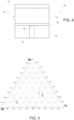
- FIG 4 shows a phase change memory element (hereinafter, memory element 10) having a wall electrode, with a general configuration similar to the memory element 1 of Figure 1 .
- the memory element 10 of Figure 4 comprises a memory region 12 arranged between a first electrode 13 (also called heater) and a second electrode 14 (also called upper electrode).
- the first and the second electrodes 13, 14 are of an electrically conductive material, for example TiN or TaN.
- the first electrode 13 has a very small width, such as to define a contact area 18 with the memory region 12 of small dimensions (for example a few nanometers); in particular, the contact area between the first electrode 13 and the memory region 12 is much smaller than the contact area between the memory region 12 and the second electrode 14.
- the first electrode 13 is formed in a dielectric layer 15.
- the first electrode 13 may be formed in a pore or an elongated trench formed in the dielectric layer 15; in this second case (wall configuration), it extends transversely to the memory region 12.
- the dielectric layer 15 may comprise silicon oxide and/or silicon nitride.
- the memory region 12 comprises a phase change material and more precisely a GST alloy, wherein the average percentage of germanium is higher than 50%, as described in detail below.
- the memory region 12 is here formed by an interface layer 16 and by a storage portion 17, both of phase change material but with different stoichiometries.
- the percentage of germanium is higher than 50%, as described in detail below.
- the interface layer 16 extends above the first electrode 13 and the dielectric layer 15, in direct electrical contact with the first electrode 13.
- the storage portion 17 extends above the interface layer 16, between the latter and the second electrode 14.
- the interface layer 16 may have a thickness comprised between 0 and 10 nanometers.
- the interface layer 16 has a thickness equal to about one tenth of the memory region 12.
- the interface layer 16 may have a thickness of 5 nanometers and the storage region 17 a thickness of 45 nm.
- the memory region 12 comprises a GST alloy.
- the storage portion 17 comprises a GST (germanium-antimony-tellurium) alloy having a percentage of germanium higher than or equal to 50% and a percentage of electrically relevant nitrogen.
- GST germanium-antimony-tellurium
- the GST alloy forming the storage portion 17 may be based on the GST 712 (Ge 7 SbiTe 2 ) alloy, also called theta alloy.
- percentage of electrically relevant nitrogen means a compositional percentage of nitrogen comprised between 5% and 25% (boundaries included).
- the storage portion 17 is formed by a quaternary alloy based on germanium Ge, antimony Sb, tellurium Te and nitrogen N (Ge x Sb y Te z N j ), wherein the percentage of nitrogen is comprised between 5% and 25 %, preferably between 8% and 21%, more preferably between 11% and 18%, even more preferably between 13% and 15%; for example, the percentage of nitrogen is equal to 14%.
- the Applicant has observed that the addition of amounts of nitrogen in percentages within the above ranges allows the crystallization temperature of the alloy to be increased. In this way, it is possible to increase the retention capability of the memory region 12 (and, in particular, of the storage portion 17) following thermal treatments, for example after soldering the chip embedding the memory on a board meeting the JEDEC standard J-STD-020C. This also allows the use of the memory element in the automotive field as to the temperature retention characteristics (compliance after thermal treatment - High Temperature Data Retention, HTDR).
- the storage portion 17 contains an alloy comprised between the alloy having stoichiometry Ge 68 Sb 09 Te 18 N 05 and the alloy having stoichiometry Ge 60 Sb 05 Te 10 N 25 .
- the percentage of nitrogen is comprised between 8% and 21% (boundaries included), more preferably between 11% and 18% (boundaries included), even more preferably between 13% and 15% (boundaries included); for example, the percentage of nitrogen is equal to 14%.
- the percentage of germanium is comprised between 60% and 68%, preferably between 61% and 67%, more preferably between 62% and 66%, even more preferably between 63% and 65%, for example it is equal to 64%.
- the percentage of antimony is comprised between 9% and 50 , preferably between 8% and 6% , for example it is equal to 7%.
- the percentage of tellurium is comprised between 18% and 10%, preferably between 17% and 12%, more preferably between 16% and 14%, for example it is equal to 15%.
- the alloy of the storage portion 17 indicated above may include other residual ions/atoms and/or impurity elements which do not alter the basic operating principles and physical characteristics of the GSTN alloy in terms of chemical and morphological distribution of ions.
- impurity element means any element not belonging to the group: germanium, antimony, tellurium and nitrogen, for example carbon, oxygen, argon, hydrogen.
- impurity elements are generally present to an undetectable extent and in any case to an extent lower than or equal to 2.0%.
- the sum of the percentages of germanium, antimony, tellurium and nitrogen (and possible impurity elements) is 100%.
- the alloy used for the storage region 17 has stoichiometry Ge 64 Sb 07 Te 15 N 14 .
- the interface layer 16 comprises a GST alloy leaner in germanium and richer in tellurium and antimony than the storage portion 17; for example, the interface layer 16 has a percentage of tellurium higher than 45% and/or a percentage of germanium lower than 40%.
- GST alloys are considered having stoichiometry Ge 22 Sb 22 Te 56 (GST225 alloy) or Ge 27 Sb 27 Te 46 (GST447 alloy) and intermediate alloys, with a variation of ⁇ 1% of the different elements.
- alloys having a percentage of germanium comprised between 21% and 28%, a percentage of antimony comprised between 21% and 27%, and a percentage of tellurium comprised between 45% and 55% are also usable.
- the alloy of the interface layer 16 indicated above may include other residual ions/atoms and/or impurity elements which do not alter the basic operating principles and physical characteristics of the alloy in terms of chemical and morphological distribution of ions.
- the sum of the percentages of germanium, antimony and tellurium (and possible impurity elements) is 100%.
- Figure 5 shows a ternary diagram of the sole elements Ge, Sb and Te, having the regions relating to the usable alloys, defined above, for forming the storage portion 17 highlighted, without considering the nitrogen concentration.
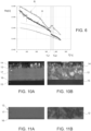
- Figure 6 shows the dependence of the resistivity ⁇ (measured in ⁇ cm), of non-defined layers - on an unpatterned wafer - formed using the theta alloy (GST 712 alloy, without addiction of nitrogen, curve A) and the GST 712 alloy with addition of nitrogen (curve B).
- these curves have been obtained starting from amorphous-state material, gradually increasing the temperature up to about 450°C, for example using a slow ramp, with a speed of 10°C/min, so as to induce the crystallization of the material and then reducing the temperature down to room temperature, for example using a ramp rate similar to the previous one, to measure the resistivity of the crystalline state.
- both alloys have a generally similar behavior, with a reduction in resistivity as the temperature increases (upper branch of curves A, B); one step downwards at a temperature called crystallization temperature (Tx1, for curve A, theta alloy without further doping, and Tx2, for curve B, N-doped theta alloy), which causes the phase transition) and the more or less constant maintenance of the resistivity value while reducing the temperature (lower branch of curves A, B).
- Tx1 crystallization temperature
- Tx2 for curve A, theta alloy without further doping
- Tx2 for curve B, N-doped theta alloy
- the Ge x Sb y Te z N J alloy has a higher crystallization temperature than the theta alloy.
- the Ge x Sb y Te z N J alloy also has an electrical behavior comparable to that of other alloys, as shown in the comparative examples of Figures 7A, 7B, 8A, 8B, 9A and 9B .
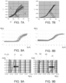
- Figure 7A shows the current-voltage curves I-V of a plurality of phase change memory elements (hereinafter also referred to as memory cells) using a GST 447 alloy.
- the curve portions increasing in an approximately linear manner at 45° relate to memory cells programmed to the crystalline state (set memory cells, logic "1"), having substantially resistive behavior;
- the curve portions (barely visible, sections D) having zero current (up to about 1V) relate to memory cells programmed to the amorphous state (reset memory cells, logic "0”), and therefore nonconductive.
- Figure 7B shows the current-voltage curves I-V of a plurality of memory cells using the above-described Ge x Sb y Te z N J alloy.
- the curves of Figure 7B also show the same type of trend described above, but the memory cells in the amorphous state change state at higher voltage, demonstrating, on the one hand, the correct electrical behavior and, on the other, the increase of the threshold voltage for the amorphous phase obtained with the Ge x Sb y Te z N J alloy, ensuring a further margin on the usable reading voltage.
- Figure 8A shows the plot of the resistance of memory cells using a GST 447 alloy after the application of current pulses I having increasing value (on the abscissa), in case of cells programmed to the set state.
- the memory cells maintain approximately constant resistance, with a very low value; as the current pulses increase, the curves begin to modify their trend, following the melting of the memory region subject to phase change (similarly to the phase change portion 9 having a semi-cylindrical or hemispherical shape of Figure 1 ), reaching the amorphous state, having higher resistance.
- Figure 8B shows the similar plot of the resistance of memory cells using the above-described Ge x Sb y Te z N J alloy. As noted, the curves of Figure 8B also show the same type of trend described above, ensuring correct electrical behavior.
- Figure 9A shows the resistance shift in a plurality of memory cells using a GST 447 alloy before and after heating for 1h at 180°C.
- curve F1,G1 represents the resistance measured on a plurality of memory cells programmed to the set state before and after annealing (the points are substantially superimposed and therefore the two plots are substantially indistinguishable);
- curve H1 shows the resistance measured on a plurality of memory cells programmed to the reset state, before thermal treatment, and
- curve J1 shows the measurements on the same memory cells programmed to the reset state, after heating.
- the points of curve J1 are shifted to the left, approaching curves F1, G1 and thus creating reading errors (JEDEC non-compliance).
- Figure 9B shows the similar plot of the resistance of phase change memory cells using the above-described Ge x Sb y Te z N J alloy.
- the curves identified by F2, G2, H2, J2 refer to measurements taken in memory cells programmed to the set state and in memory cells programmed to the reset state, similarly to the measurements F1-J1 indicated by the same letter.
- curves F2, G2 of Figure 9B have a greater differentiation, with respect to curves F1, G1 of Figure 9A , as to the memory cells programmed to the reset state, curve J2, after heating, is shifted in the opposite direction with respect to the corresponding curve J1 of Figure 9B and precisely in direction of a greater resistance difference from the memory cells programmed to the set state.
- memory cells formed with the above-described Ge x Sb y Te z N J alloy not only do not have retention problems after heating, but even better discernibility as to the average (typical) behavior of the memory cells.
- the interface layer 16 improves the adhesion between the phase change chalcogenic material of the memory region 12 and the dielectric layer 15.
- the memory element 10 undergoes a slight deterioration in its retention capabilities, due to the average reduction of germanium in the memory region 12, but has an improvement in cycling (and therefore in the possibility of allowing modification of the written datum).
- the thickness of the interface layer 16 may vary according to the needs, even if the values indicated above, and in particular the value of 5 nm, provide an optimal trade-off in most cases, with improvement of the adhesion and negligible degradation of the retention.
- the portion of the memory region 12 above the contact area 18 forms a phase change portion with a semi-cylindrical or hemispherical shape, similarly to what discussed with reference to Figure 1 for the phase change portion 9.
- the studies have shown that, during manufacturing and following thermal treatments which occur in the final manufacturing steps and/or during operation, the interface layer 16 is no longer distinguishable from the storage portion 17, as shown by way of example in Figures 10A, 10B, 11A and 11B , which, indeed, show the aggregation and gettering effect exerted by the interface layer 16 on the germanium atoms/ions, with formation of clusters of germanium in the zone where the interface layer 16 had been initially deposited.
- the memory elements 10 formed with the Ge x Sb y Te z N J alloy and provided with an interface layer 16 show a high crystallization temperature capable of ensuring compliance with the soldering reflow profile required by the JEDEC standard, with HTDR data retention meeting the stringent automotive and embedded memory requirements, such as for IoT (Internet on Things) applications, SmartCards and the like.
- IoT Internet on Things
Landscapes
- Chemical & Material Sciences (AREA)
- Engineering & Computer Science (AREA)
- Materials Engineering (AREA)
- Mechanical Engineering (AREA)
- Metallurgy (AREA)
- Organic Chemistry (AREA)
- Crystallography & Structural Chemistry (AREA)
- Semiconductor Memories (AREA)
Abstract
Disclosed is a phase change memory element (10) having a memory region (12) arranged between first and second electrodes (13, 14) and comprising a GST alloy, wherein the average percentage of germanium is higher than 50%. The memory region (12) has a storage portion (17) formed by a GST alloy including nitrogen in an electrically relevant amount, preferably having a percentage of germanium between 60% and 68%, a percentage of antimony between 5% and 9%, a percentage of tellurium between 10% and 18%, and a percentage of nitrogen between 5% and 25%, most preferably based on a GST-712 alloy, between Ge68Sb9Te18N5 and Ge60Sb5Te10N25.
Description
- The present invention relates to a phase change memory element particularly suitable for embedded and automotive applications.
- As is known, non-volatile phase change memories (PCMs) use materials that may switch between two or more stable states characterized by different electrical properties. For instance, such materials are able to switch between a disorderly, amorphous, phase and an orderly, crystalline or polycrystalline phase, and the two phases are associated to resistivities having considerably different values that may be used to store data.
- To this end, the chemical elements of Group VI of the Periodic Table, such as tellurium (Te), selenium (Se), germanium (Ge) or antimony (Sb), referred to as chalcogenides or chalcogenic materials, are commonly used.
- Phase changes are obtained by locally increasing the temperature of the cells of chalcogenic material, through resistive electrodes (generally known as heaters) arranged in contact with respective regions of chalcogenic material.
- For example,
Figure 1 shows cross-section of a phasechange memory element 1, with a wall-shaped heater. - Phase
change memory element 1 includes amemory region 2 of a chalcogenic material, in contact with afirst electrode 3, here a bottom electrode, and with asecond electrode 4, here an upper electrode. -
Memory region 2 may be a GexSbyTez alloy (also known as GST alloy). -
Electrodes first electrode 3 has a very small width, such as to define a smaller contact area with respect to thesecond electrode 4. For example, thefirst electrode 3 may have a width of a few nanometers and be formed in a pore or in an elongated trench in a dielectric layer 5 (the latter configuration, also called wall configuration). In particular, in case thefirst electrode 3 extends in an elongated trench, it extends transversely to the memory region. - A selection device (for example, a MOSFET, not shown) is connected to the first electrode/
heater 3 and enables passage of an electric current that, by Joule effect, heats the chalcogenic material to obtain the desired temperature for phase change. - Due to the small width of the
first electrode 3, current flowing in thefirst electrode 3 is concentrated and causes heating of a portion of thememory region 2 above a contact area 8 (phase change portion 9, having semi-cylindrical or hemispherical shape). Therefore, thefirst electrode 3 acts as a heater. - In particular, to program the phase
change memory element 1 to its crystalline state (low resistance state, also called set state), an electrical pulse is applied to heat thememory region 2, and in particular thephase change portion 9, above its crystallization temperature. By allowing thememory region 2 to slowly cool down to normal operating temperature, thephase change portion 9 maintains the polycrystalline phase. See, e.g.,Figure 2A . - To program the phase
change memory element 1 to the amorphous phase (high resistance state, also called reset state, writing), the material is heated at a higher temperature than the set state programming temperature, inducing the melting of the chalcongenide. By abruptly cutting off the electrical current pulse, the sudden cooling down of the phase change material prevents the reconfiguration thereof to the polycrystalline phase allowing solidification in a disorderly phase (amorphous phase). See, e.g.,Figure 2B . -
Figure 3 shows possible plots of temperature T as a function of time t for programming the phase change memory element with a reset pulse (continuous line) and a set pulse (dotted line) in the ideal condition of uniform temperature in thewhole memory region 2. In fact, a decreasing temperature gradient is present, from thefirst electrode 3 to thesecond electrode 4, within the phase change memory element. In any case,phase change portion 9 follows the shown behavior reported inFigure 3 . - During reading, the state of the chalcogenic material is detected by applying a voltage that is sufficiently low as avoid an excessive heating, and then by reading the current flowing in the
memory element 1. Since the current is proportional to the conductivity of phasechange memory element 1, it is possible to determine in which state the memory element is and therefore read the stored datum. - Memories including phase change memory elements are one of the most promising type of memory due to their easy integration with advanced logics and their costs, but their reliability is still not always sufficient to meet the requirements existing in some applications.
- In fact, traditionally, for forming the memory region (2, in
Figure 1 ), among the available GST materials, the (Ge2Sb2Te5) 225 alloy has been widely preferred and studied, owing to its excellent crystallization and stability properties. However, it has shown retention problems of the amorphous phase (used to identify the logic state 0) at high temperature. - Therefore, different alloys have been proposed; for example, it has been proposed to dope the 225 alloy with impurities, to obtain higher crystallization temperatures, better structural and thermal stability as well as higher switching speed.
- Further research has instead been directed towards Geenriched alloys, i.e. alloys in which Ge is a predominant component of the average composition (also called Ge-rich alloys), which have shown an increase in the crystallization temperature, so as to obtain a greater capability to preserve the datum, without degrading the cycling performances (data retention and endurance).
- In particular, in these alloys, the percentage of Ge in the GST alloy may be higher than 50%.
- However, these solutions do not allow to fully meet the strict requirements existing in automotive applications or for memories embedded in an embedded device or circuit (such as a processor, calculation unit and the like), so-called "embedded" memories, in particular due to thermal treatments of the memory performed during the final processing steps (assembly of the die on the board and/or on packaged devices) or during operation and which may cause poor data retention.
-
US 2021/249592 A1 andWO 2011/1191175A1 -
US 2014/376309 A1 andUS 2022/020923 disclose other phase change memories, program methods and cell structure. - The aim of the present invention is to provide a memory device overcoming the drawbacks of the prior art.
- According to the present invention a phase change memory element is provided, as defined in the appended claims.
- For a better understanding of the present invention, an embodiment thereof is now described, purely by way of nonlimiting example, with reference to the attached drawings, wherein:
-
Figure 1 is a cross-section of a phase change memory element; -
Figures 2A and 2B are images obtained through electron Dark Field (DF) Scanning Transmission Electron Microscope (STEM) of the phase change memory element ofFigure 1 , in the set state and, respectively, in the reset state; -
Figure 3 shows exemplary plots of temperatures versus time during set/reset operations of the phase change memory cell ofFigure 1 ; -
Figure 4 is a cross-section of a phase change memory element according to the present disclosure; -
Figure 5 shows a ternary diagram representing the relative amounts of ions/atoms in a region comprising a GST alloy; -
Figure 6 shows the plot of the resistivity as a function of temperature for a GST alloy of the ternary diagram ofFigure 5 and for a nitrogen-enriched GST alloy, as described below; -
Figures 7A-7B show current-voltage curves measured in a plurality of memory elements using respectively aGST 447 alloy and an alloy according to the present disclosure; -
Figures 8A-8B show resistance plots following the application of current pulses in a plurality of memory elements using, respectively, aGST 447 alloy and an alloy according to the present disclosure; -
Figures 9A-9B show the resistance change for the set state and for the reset state caused by heating in a plurality of memory elements using, respectively, aGST 447 alloy and an alloy according to the present disclosure; -
Figures 10A and 10B are images obtained through electron Dark Field (DF) Scanning Transmission Electron Microscope (STEM) of the phase change memory element ofFigure 4 , immediately after deposition of the various layers and, respectively, after thermal treatment steps; and -
Figures 11A and 11B are images obtained through EELS (Electron Energy Loss Spectroscopy) technique of the phase change memory element ofFigure 4 , immediately after deposition of the various layers and, respectively, after thermal treatment steps. -
Figure 4 shows a phase change memory element (hereinafter, memory element 10) having a wall electrode, with a general configuration similar to thememory element 1 ofFigure 1 . - In detail, the
memory element 10 ofFigure 4 comprises amemory region 12 arranged between a first electrode 13 (also called heater) and a second electrode 14 (also called upper electrode). - The first and the
second electrodes - Similarly to
Figure 1 , thefirst electrode 13 has a very small width, such as to define acontact area 18 with thememory region 12 of small dimensions (for example a few nanometers); in particular, the contact area between thefirst electrode 13 and thememory region 12 is much smaller than the contact area between thememory region 12 and thesecond electrode 14. - The
first electrode 13 is formed in adielectric layer 15. For example, thefirst electrode 13 may be formed in a pore or an elongated trench formed in thedielectric layer 15; in this second case (wall configuration), it extends transversely to thememory region 12. - For example, the
dielectric layer 15 may comprise silicon oxide and/or silicon nitride. - The
memory region 12 comprises a phase change material and more precisely a GST alloy, wherein the average percentage of germanium is higher than 50%, as described in detail below. - In particular, the
memory region 12 is here formed by aninterface layer 16 and by astorage portion 17, both of phase change material but with different stoichiometries. Preferably, in thestorage portion 17, the percentage of germanium is higher than 50%, as described in detail below. - The
interface layer 16 extends above thefirst electrode 13 and thedielectric layer 15, in direct electrical contact with thefirst electrode 13. - The
storage portion 17 extends above theinterface layer 16, between the latter and thesecond electrode 14. - The
interface layer 16 may have a thickness comprised between 0 and 10 nanometers. For example, theinterface layer 16 has a thickness equal to about one tenth of thememory region 12. - For example, for a
memory region 12 having a thickness of about 50 nanometers, theinterface layer 16 may have a thickness of 5 nanometers and the storage region 17 a thickness of 45 nm. - As indicated above, the
memory region 12 comprises a GST alloy. - Specifically, the
storage portion 17 comprises a GST (germanium-antimony-tellurium) alloy having a percentage of germanium higher than or equal to 50% and a percentage of electrically relevant nitrogen. - In particular, the GST alloy forming the
storage portion 17 may be based on the GST 712 (Ge7SbiTe2) alloy, also called theta alloy. - Furthermore, the expression "percentage of electrically relevant nitrogen" means a compositional percentage of nitrogen comprised between 5% and 25% (boundaries included).
- In particular, according to the present disclosure, the
storage portion 17 is formed by a quaternary alloy based on germanium Ge, antimony Sb, tellurium Te and nitrogen N (GexSbyTezNj), wherein the percentage of nitrogen is comprised between 5% and 25 %, preferably between 8% and 21%, more preferably between 11% and 18%, even more preferably between 13% and 15%; for example, the percentage of nitrogen is equal to 14%. - The Applicant has observed that the addition of amounts of nitrogen in percentages within the above ranges allows the crystallization temperature of the alloy to be increased. In this way, it is possible to increase the retention capability of the memory region 12 (and, in particular, of the storage portion 17) following thermal treatments, for example after soldering the chip embedding the memory on a board meeting the JEDEC standard J-STD-020C. This also allows the use of the memory element in the automotive field as to the temperature retention characteristics (compliance after thermal treatment - High Temperature Data Retention, HTDR).
- In particular, according to the present disclosure, the
storage portion 17 contains an alloy comprised between the alloy having stoichiometry Ge68Sb09Te18N05 and the alloy having stoichiometry Ge60Sb05Te10N25. - In particular, the percentage of nitrogen is comprised between 8% and 21% (boundaries included), more preferably between 11% and 18% (boundaries included), even more preferably between 13% and 15% (boundaries included); for example, the percentage of nitrogen is equal to 14%.
- The percentage of germanium is comprised between 60% and 68%, preferably between 61% and 67%, more preferably between 62% and 66%, even more preferably between 63% and 65%, for example it is equal to 64%.
- Furthermore, the percentage of antimony is comprised between 9% and 50 , preferably between 8% and 6% , for example it is equal to 7%.
- The percentage of tellurium is comprised between 18% and 10%, preferably between 17% and 12%, more preferably between 16% and 14%, for example it is equal to 15%.
- Furthermore, the alloy of the
storage portion 17 indicated above may include other residual ions/atoms and/or impurity elements which do not alter the basic operating principles and physical characteristics of the GSTN alloy in terms of chemical and morphological distribution of ions. - In the present disclosure, "impurity element" means any element not belonging to the group: germanium, antimony, tellurium and nitrogen, for example carbon, oxygen, argon, hydrogen.
- These impurity elements are generally present to an undetectable extent and in any case to an extent lower than or equal to 2.0%.
- Obviously, as clear to the person skilled in the art, in the alloy of the
storage portion 17, the sum of the percentages of germanium, antimony, tellurium and nitrogen (and possible impurity elements) is 100%. - In particular, the alloy used for the
storage region 17 has stoichiometry Ge64Sb07Te15N14. - The
interface layer 16 comprises a GST alloy leaner in germanium and richer in tellurium and antimony than thestorage portion 17; for example, theinterface layer 16 has a percentage of tellurium higher than 45% and/or a percentage of germanium lower than 40%. - For example, according to the present disclosure, for the
interface layer 16, GST alloys are considered having stoichiometry Ge22Sb22Te56 (GST225 alloy) or Ge27Sb27Te46 (GST447 alloy) and intermediate alloys, with a variation of ±1% of the different elements. - Therefore, alloys having a percentage of germanium comprised between 21% and 28%, a percentage of antimony comprised between 21% and 27%, and a percentage of tellurium comprised between 45% and 55% are also usable.
- Furthermore, the alloy of the
interface layer 16 indicated above may include other residual ions/atoms and/or impurity elements which do not alter the basic operating principles and physical characteristics of the alloy in terms of chemical and morphological distribution of ions. - Obviously, as clear to the person skilled in the art, for the
interface layer 16, the sum of the percentages of germanium, antimony and tellurium (and possible impurity elements) is 100%. -
Figure 5 shows a ternary diagram of the sole elements Ge, Sb and Te, having the regions relating to the usable alloys, defined above, for forming thestorage portion 17 highlighted, without considering the nitrogen concentration. - For the alloys indicated by a star and for the alloy having stoichiometry Ge64Sb07Te25N14, comparative tests have been carried out as to crystallization temperature, functionality and retention capability, described hereinbelow with reference to
Figures 6-10B . -
Figure 6 shows the dependence of the resistivity ρ (measured in Ω·cm), of non-defined layers - on an unpatterned wafer - formed using the theta alloy (GST 712 alloy, without addiction of nitrogen, curve A) and the GST 712 alloy with addition of nitrogen (curve B). - In particular, these curves have been obtained starting from amorphous-state material, gradually increasing the temperature up to about 450°C, for example using a slow ramp, with a speed of 10°C/min, so as to induce the crystallization of the material and then reducing the temperature down to room temperature, for example using a ramp rate similar to the previous one, to measure the resistivity of the crystalline state.
- As noted, both alloys have a generally similar behavior, with a reduction in resistivity as the temperature increases (upper branch of curves A, B); one step downwards at a temperature called crystallization temperature (Tx1, for curve A, theta alloy without further doping, and Tx2, for curve B, N-doped theta alloy), which causes the phase transition) and the more or less constant maintenance of the resistivity value while reducing the temperature (lower branch of curves A, B).
- As noted, the GexSbyTezNJ alloy has a higher crystallization temperature than the theta alloy.
- The GexSbyTezNJ alloy also has an electrical behavior comparable to that of other alloys, as shown in the comparative examples of
Figures 7A, 7B, 8A, 8B, 9A and 9B . - In detail,
Figure 7A shows the current-voltage curves I-V of a plurality of phase change memory elements (hereinafter also referred to as memory cells) using aGST 447 alloy. In these curves, the curve portions increasing in an approximately linear manner at 45° (with a positive slope representative of a series resistance of the first electrode - heater 13 - sections C) relate to memory cells programmed to the crystalline state (set memory cells, logic "1"), having substantially resistive behavior; the curve portions (barely visible, sections D) having zero current (up to about 1V) relate to memory cells programmed to the amorphous state (reset memory cells, logic "0"), and therefore nonconductive. For these latter curve portions, after the value of about 1V, an electronic switching phenomenon occurs and the curves abruptly modify their trend and, after a transition phase detectable from the negative-slope portions (sections E), follow the trend at, approximately, +45°C of the curves of the memory cells programmed to the crystalline state. -
Figure 7B shows the current-voltage curves I-V of a plurality of memory cells using the above-described GexSbyTezNJ alloy. As noted, the curves ofFigure 7B also show the same type of trend described above, but the memory cells in the amorphous state change state at higher voltage, demonstrating, on the one hand, the correct electrical behavior and, on the other, the increase of the threshold voltage for the amorphous phase obtained with the GexSbyTezNJ alloy, ensuring a further margin on the usable reading voltage. -
Figure 8A shows the plot of the resistance of memory cells using aGST 447 alloy after the application of current pulses I having increasing value (on the abscissa), in case of cells programmed to the set state. - As noted, initially the memory cells maintain approximately constant resistance, with a very low value; as the current pulses increase, the curves begin to modify their trend, following the melting of the memory region subject to phase change (similarly to the
phase change portion 9 having a semi-cylindrical or hemispherical shape ofFigure 1 ), reaching the amorphous state, having higher resistance. -
Figure 8B shows the similar plot of the resistance of memory cells using the above-described GexSbyTezNJ alloy. As noted, the curves ofFigure 8B also show the same type of trend described above, ensuring correct electrical behavior. -
Figure 9A shows the resistance shift in a plurality of memory cells using aGST 447 alloy before and after heating for 1h at 180°C. In detail, the curve on the left (curve F1,G1) represents the resistance measured on a plurality of memory cells programmed to the set state before and after annealing (the points are substantially superimposed and therefore the two plots are substantially indistinguishable); curve H1 shows the resistance measured on a plurality of memory cells programmed to the reset state, before thermal treatment, and curve J1 shows the measurements on the same memory cells programmed to the reset state, after heating. As noted, the points of curve J1 are shifted to the left, approaching curves F1, G1 and thus creating reading errors (JEDEC non-compliance). -
Figure 9B shows the similar plot of the resistance of phase change memory cells using the above-described GexSbyTezNJ alloy. In this Figure, the curves identified by F2, G2, H2, J2 refer to measurements taken in memory cells programmed to the set state and in memory cells programmed to the reset state, similarly to the measurements F1-J1 indicated by the same letter. - As noted, not only curves F2, G2 of
Figure 9B have a greater differentiation, with respect to curves F1, G1 ofFigure 9A , as to the memory cells programmed to the reset state, curve J2, after heating, is shifted in the opposite direction with respect to the corresponding curve J1 ofFigure 9B and precisely in direction of a greater resistance difference from the memory cells programmed to the set state. - Consequently, memory cells formed with the above-described GexSbyTezNJ alloy, not only do not have retention problems after heating, but even better discernibility as to the average (typical) behavior of the memory cells.
- Studies by the Applicant have also shown that the
interface layer 16 improves the adhesion between the phase change chalcogenic material of thememory region 12 and thedielectric layer 15. - Furthermore, since, after depositing the
storage portion 17 and the subsequent processing steps, the chemical elements of theinterface layer 16 and of thestorage portion 17 mix, thememory element 10 undergoes a slight deterioration in its retention capabilities, due to the average reduction of germanium in thememory region 12, but has an improvement in cycling (and therefore in the possibility of allowing modification of the written datum). - In particular, the thickness of the
interface layer 16 may vary according to the needs, even if the values indicated above, and in particular the value of 5 nm, provide an optimal trade-off in most cases, with improvement of the adhesion and negligible degradation of the retention. - Studies carried out by the Applicant have shown that, in use, the portion of the
memory region 12 above thecontact area 18 forms a phase change portion with a semi-cylindrical or hemispherical shape, similarly to what discussed with reference toFigure 1 for thephase change portion 9. - Furthermore, the studies have shown that, during manufacturing and following thermal treatments which occur in the final manufacturing steps and/or during operation, the
interface layer 16 is no longer distinguishable from thestorage portion 17, as shown by way of example inFigures 10A, 10B, 11A and 11B , which, indeed, show the aggregation and gettering effect exerted by theinterface layer 16 on the germanium atoms/ions, with formation of clusters of germanium in the zone where theinterface layer 16 had been initially deposited. - As a result, the
memory elements 10 formed with the GexSbyTezNJ alloy and provided with aninterface layer 16 show a high crystallization temperature capable of ensuring compliance with the soldering reflow profile required by the JEDEC standard, with HTDR data retention meeting the stringent automotive and embedded memory requirements, such as for IoT (Internet on Things) applications, SmartCards and the like. - Finally, it is clear that modifications and variations may be made to the phase change memory element described and illustrated herein without thereby departing from the scope of the present invention, as defined in the attached claims.
Claims (15)
- A phase change memory element (10) comprising a memory region (12), a first electrode (13) and a second electrode (14),
wherein:the memory region (12) is arranged between the first and the second electrodes (13, 14);the memory region (12) comprises a germanium-antimony-tellurium -GST alloy, with an average percentage of germanium higher than or equal to 50%, andthe memory region (12) comprises a storage portion (17) including nitrogen in an electrically relevant amount. - The phase change memory element according to claim 1, wherein the storage portion (17) is formed by an alloy including:a percentage of germanium comprised between 60% and 68%;a percentage of antimony comprised between 9% and 5%;a percentage of tellurium comprised between 18% and 10%; anda percentage of nitrogen comprised between 5% and 25%.
- The phase change memory element according to claim 1 or 2, wherein the percentage of nitrogen is comprised between 8% and 21%, preferably between 11% and 18%, more preferably between 13% and 15%.
- The phase change memory element according to any of the preceding claims, wherein the percentage of nitrogen is equal to 14% .
- The phase change memory element according to any of the preceding claims, wherein the percentage of germanium is comprised between 61% and 67%, preferably between 62% and 66%, more preferably between 63% and 65%.
- The phase change memory element according to any of the preceding claims, wherein the percentage of germanium is equal to 64%.
- The phase change memory element according to any of the preceding claims, wherein the percentage of antimony is comprised between 8% and 6%.
- The phase change memory element according to any of the preceding claims, wherein the percentage of antimony is equal to 7%.
- The phase change memory element according to any of the preceding claims, wherein the percentage of tellurium is comprised between 17% and 12%, preferably between 16% and 14%.
- The phase change memory element according to any of the preceding claims, wherein the percentage of tellurium is equal to 15%.
- The phase change memory element according to any of the preceding claims, wherein the memory region (12) further comprises an interface layer (16) formed by a GST alloy having lower germanium content with respect to the storage portion (17).
- The phase change memory element according to the preceding claim, wherein the interface layer (16) contains a percentage of tellurium higher than 45% and a percentage of germanium lower than 40%.
- The phase change memory element according to any of claims 11-12, wherein the interface layer (16) comprises a percentage of germanium comprised between 21% and 28%, a percentage of antimony comprised between 21% and 27% and a percentage of tellurium comprised between 45% and 55%.
- The phase change memory element according to any of the preceding claims, wherein the first electrode (13) has a wall or pore shape and has a first contact area (18) with the memory region (12) and the second electrode (14) has a second contact area with the memory region (12), the first contact area (18) having a smaller dimension than the second contact area.
- The phase change memory element according to the preceding claim, wherein the memory region (12) comprises an interface layer (16), the interface layer (16) is in direct contact with the first electrode (13) and the storage portion (17) is in direct contact with the second electrode (14).
Applications Claiming Priority (1)
| Application Number | Priority Date | Filing Date | Title |
|---|---|---|---|
| IT102023000009990A IT202300009990A1 (en) | 2023-05-17 | 2023-05-17 | PHASE CHANGE MEMORY ELEMENT PARTICULARLY SUITABLE FOR EMBEDDED AND AUTOMOTIVE APPLICATIONS |
Publications (1)
| Publication Number | Publication Date |
|---|---|
| EP4465804A1 true EP4465804A1 (en) | 2024-11-20 |
Family
ID=87245561
Family Applications (1)
| Application Number | Title | Priority Date | Filing Date |
|---|---|---|---|
| EP24175018.1A Pending EP4465804A1 (en) | 2023-05-17 | 2024-05-09 | Phase change memory element particularly suitable for embedded and automotive applications |
Country Status (4)
| Country | Link |
|---|---|
| US (1) | US20240389484A1 (en) |
| EP (1) | EP4465804A1 (en) |
| CN (1) | CN119012902A (en) |
| IT (1) | IT202300009990A1 (en) |
Citations (5)
| Publication number | Priority date | Publication date | Assignee | Title |
|---|---|---|---|---|
| WO2011119175A1 (en) * | 2010-03-26 | 2011-09-29 | Advanced Technology Materials, Inc. | Germanium antimony telluride materials and devices incorporating same |
| US20140376309A1 (en) | 2013-06-21 | 2014-12-25 | Macronix International Co., Ltd. | Phase change memory material and system for embedded memory applications |
| US20210249592A1 (en) | 2020-02-07 | 2021-08-12 | Taiwan Semiconductor Manufacturing Company Limited | Phase-change random access memory device and method of making the same |
| US20220020923A1 (en) | 2020-07-15 | 2022-01-20 | Commissariat à l'énergie atomique et aux énergies alternatives | Phase-change material and associated resistive phase-change memory |
| EP4187540A1 (en) * | 2021-11-30 | 2023-05-31 | STMicroelectronics S.r.l. | Phase change memory device with improved retention characteristics and related method |
-
2023
- 2023-05-17 IT IT102023000009990A patent/IT202300009990A1/en unknown
-
2024
- 2024-05-09 EP EP24175018.1A patent/EP4465804A1/en active Pending
- 2024-05-09 US US18/659,436 patent/US20240389484A1/en active Pending
- 2024-05-16 CN CN202410607385.1A patent/CN119012902A/en active Pending
Patent Citations (5)
| Publication number | Priority date | Publication date | Assignee | Title |
|---|---|---|---|---|
| WO2011119175A1 (en) * | 2010-03-26 | 2011-09-29 | Advanced Technology Materials, Inc. | Germanium antimony telluride materials and devices incorporating same |
| US20140376309A1 (en) | 2013-06-21 | 2014-12-25 | Macronix International Co., Ltd. | Phase change memory material and system for embedded memory applications |
| US20210249592A1 (en) | 2020-02-07 | 2021-08-12 | Taiwan Semiconductor Manufacturing Company Limited | Phase-change random access memory device and method of making the same |
| US20220020923A1 (en) | 2020-07-15 | 2022-01-20 | Commissariat à l'énergie atomique et aux énergies alternatives | Phase-change material and associated resistive phase-change memory |
| EP4187540A1 (en) * | 2021-11-30 | 2023-05-31 | STMicroelectronics S.r.l. | Phase change memory device with improved retention characteristics and related method |
Also Published As
| Publication number | Publication date |
|---|---|
| CN119012902A (en) | 2024-11-22 |
| IT202300009990A1 (en) | 2024-11-17 |
| US20240389484A1 (en) | 2024-11-21 |
Similar Documents
| Publication | Publication Date | Title |
|---|---|---|
| CN113169272B (en) | Multi-level phase change memory cells and manufacturing methods thereof | |
| US7786462B2 (en) | Chalcogenide devices exhibiting stable operation from the as-fabricated state | |
| KR100564608B1 (en) | Phase change memory device | |
| KR101730561B1 (en) | Variable resistance materials with superior data retention characteristics | |
| KR102607859B1 (en) | Phase change memory device including two-dimensional material and method of operating the same | |
| US9105842B2 (en) | Method for manufacturing a carbon-based memory element and memory element | |
| JP5403565B2 (en) | Phase change material and phase change type memory device | |
| US10892409B2 (en) | Switching device, method of fabricating the same, and non-volatile memory device having the same | |
| EP1667244A2 (en) | Phase change memory device having phase change material layer containing phase change nano particles and method of fabricating the same | |
| JP5520484B2 (en) | Chalcogenide devices and chalcogenide materials with low germanium or tellurium content | |
| US11101430B2 (en) | Storage element | |
| WO2007070218A2 (en) | Chalcogenide devices and materials having reduced germanium or telluruim content | |
| JP2009524210A5 (en) | ||
| TW200929526A (en) | Non-volatile memory and fabricating method thereof | |
| US8049202B2 (en) | Phase change memory device having phase change material layer containing phase change nano particles | |
| US20240389484A1 (en) | Phase change memory element particularly suitable for embedded and automotive applications | |
| KR20060061745A (en) | A phase change memory device having a phase change material layer including phase change nanoparticles and a method of manufacturing the same | |
| US12266402B2 (en) | Phase change memory device with improved retention characteristics and related method | |
| TWI741479B (en) | Semiconductor memory device | |
| US8217379B2 (en) | Arsenic-containing variable resistance materials | |
| US20210376236A1 (en) | Memory device | |
| KR100895797B1 (en) | Phase change element and its manufacturing method | |
| Rajendran et al. | Phase change memory—Opportunities and challenges |
Legal Events
| Date | Code | Title | Description |
|---|---|---|---|
| PUAI | Public reference made under article 153(3) epc to a published international application that has entered the european phase |
Free format text: ORIGINAL CODE: 0009012 |
|
| STAA | Information on the status of an ep patent application or granted ep patent |
Free format text: STATUS: THE APPLICATION HAS BEEN PUBLISHED |
|
| AK | Designated contracting states |
Kind code of ref document: A1 Designated state(s): AL AT BE BG CH CY CZ DE DK EE ES FI FR GB GR HR HU IE IS IT LI LT LU LV MC ME MK MT NL NO PL PT RO RS SE SI SK SM TR |
|
| STAA | Information on the status of an ep patent application or granted ep patent |
Free format text: STATUS: REQUEST FOR EXAMINATION WAS MADE |
|
| 17P | Request for examination filed |
Effective date: 20250429 |