EP4465538A1 - Delta-sigma sensing device - Google Patents
Delta-sigma sensing device Download PDFInfo
- Publication number
- EP4465538A1 EP4465538A1 EP23382470.5A EP23382470A EP4465538A1 EP 4465538 A1 EP4465538 A1 EP 4465538A1 EP 23382470 A EP23382470 A EP 23382470A EP 4465538 A1 EP4465538 A1 EP 4465538A1
- Authority
- EP
- European Patent Office
- Prior art keywords
- delta
- stage
- feedback
- low
- intramodulator
- Prior art date
- Legal status (The legal status is an assumption and is not a legal conclusion. Google has not performed a legal analysis and makes no representation as to the accuracy of the status listed.)
- Pending
Links
Images






Classifications
-
- H—ELECTRICITY
- H03—ELECTRONIC CIRCUITRY
- H03M—CODING; DECODING; CODE CONVERSION IN GENERAL
- H03M3/00—Conversion of analogue values to or from differential modulation
- H03M3/30—Delta-sigma modulation
- H03M3/458—Analogue/digital converters using delta-sigma modulation as an intermediate step
- H03M3/464—Details of the digital/analogue conversion in the feedback path
-
- H—ELECTRICITY
- H03—ELECTRONIC CIRCUITRY
- H03M—CODING; DECODING; CODE CONVERSION IN GENERAL
- H03M3/00—Conversion of analogue values to or from differential modulation
- H03M3/30—Delta-sigma modulation
- H03M3/39—Structural details of delta-sigma modulators, e.g. incremental delta-sigma modulators
- H03M3/412—Structural details of delta-sigma modulators, e.g. incremental delta-sigma modulators characterised by the number of quantisers and their type and resolution
- H03M3/422—Structural details of delta-sigma modulators, e.g. incremental delta-sigma modulators characterised by the number of quantisers and their type and resolution having one quantiser only
-
- H—ELECTRICITY
- H03—ELECTRONIC CIRCUITRY
- H03M—CODING; DECODING; CODE CONVERSION IN GENERAL
- H03M3/00—Conversion of analogue values to or from differential modulation
- H03M3/30—Delta-sigma modulation
- H03M3/458—Analogue/digital converters using delta-sigma modulation as an intermediate step
- H03M3/466—Multiplexed conversion systems
Definitions
- the object of the present invention is a delta-sigma sensing device with background signal attenuation and distributed encoding.
- Sensor technologies play a critical role in various industries, including environmental monitoring, automotive, aerospace, medical, and consumer electronics. These sensors are designed to measure and monitor different physical (e.g., pressure, temperature, humidity) and chemical (e.g., analyte concentrations) parameters, providing essential data for a wide range of applications. To enable the sensors to communicate with other devices for performing further computation, the sensors are commonly "smartened” by incorporation of integrated circuits for processing the sensor signal and converting it into a digital format readable from external user devices.
- physical e.g., pressure, temperature, humidity
- chemical e.g., analyte concentrations
- Drift refers to a slow, continuous change in the output of a sensor over time, independent of the input signal of interest. This can be attributed to aging, contamination of the sensing surface, and other environmental factors such as thermal, mechanical or electrical stress.
- Offset is a constant component in the sensor output signal, regardless of the input value. It is usually caused by manufacturing imperfections or other external influences. Inaccurate measurements may lead to incorrect decision-making, reduced system efficiency, and, in some cases, critical failures.
- Circuit methods proposed for removing or cancelling offset involve applying a bias at the device, reconfigured within a limited range during a separate calibration phase.
- the adoption of machine learning algorithms and artificial intelligence (Al) in sensor systems can also help to detect and compensate drift and offset. By analyzing historical sensor data and identifying patterns, these algorithms can predict and correct the resulting errors in real-time, leading to more accurate and reliable measurements.
- Al artificial intelligence
- electrochemical microsensors fabricated in semiconductor technologies offer advantages such as miniaturization, mass fabrication, and ease of integration with CMOS circuits for embedding signal processing as smart sensing devices.
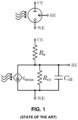
- the amperometric sensor family shown in figure 1 is particularly appealing since a simple three-microelectrode cell structure allows to evaluate redox reactions in solution at a target analyte potential (VRW) between reference (RE) and working (WE) electrodes.
- VRW target analyte potential
- RE reference
- WE working
- the counter electrode (CE) supplies all the current needed for the electrochemical reaction at the surface of the WE.
- the electrode-electrolyte interface is usually modelled as the small-signal electrical circuit of figure 1 , where i sens is the CE-WE current change to be measured, while R ct , C dl and R s stand for the charge transfer resistance, the double layer capacitance and the electrolyte solution resistance, respectively.
- Figure 2 shows a field-effect transistor (FET) sensor easy to miniaturize and replicate as sensor array in semiconductor technologies.
- the FET can be integrated as a metal-oxide-semiconductor transistor with the metal connection at the gate replaced by a liquid.
- the liquid contains the target analytes to be measured, which interact with the gate insulator functionalized as sensing surface. Changes in the analyte concentrations are transduced into a potential change at the gate insulator surface dependent upon the sensitivity to each analyte. These electrical variations in the gate potential can then be read out in the electrical domain by use of electronic circuits.
- the FET can be modelled as the electrical circuit of figure 2 , where V sens is the potential change to be measured due to a variation in the chemical contribuent V chem , while C sens stand for the sensing capacitance due to the dielectric sensing membrane.
- Drift is particularly problematic for small signals and long-term measurements as it can be difficult to identify the signal amongst the shifting baseline.
- the sensor output can be driven outside of the analogue-to-digital converter input range and saturate. This also means an analogue-to-digital converter will need to cover a wide input range, which can increase quantization noise.
- FET field-effect-transistor
- the delta-sigma sensing device of the present invention has built-in adaptive pulse modulation encoding for delivering sensor biasing, analog-to-digital conversion, and attenuation of undesired background sensor signals (e.g., DC offset, drifts) lying out of the frequency band of interest.
- undesired background sensor signals e.g., DC offset, drifts
- the device comprises one or more transducers and one or more delta-sigma modulators.
- each of the transducers comprises a sensing stage intended to detect a property of the environment such as temperature, humidity, analyte concentrations, and to convert it into an electrical input signal.
- Each transducer also comprises an interfacing stage, connected to the sensing stage, that receives the electrical input signal and feeds it as input transduced signal to one or more of the delta-sigma modulators.
- each of the delta-sigma modulators comprises an input stage, connected to the interfacing stage, for receiving an unfiltered intramodulator feedback signal and a low-pass-filtered intramodulator feedback signal, and subtracting them from a sum of one or more of the input transduced signals to obtain a delta error signal.
- each modulator comprises a feedforward low-pass filtering stage, that obtains a filtered delta error signal, and an analog-to-digital encoder, following the feedforward filtering stage, that converts the filtered delta error signal into a digital output signal d out (t).
- the modulator comprises an unfiltered intramodulator feedback path, that converts d out (t) into the unfiltered intramodulator feedback signal, and a low-pass-filtered intramodulator feedback path, between the analog-to-digital encoder and the input stage, that converts d out (t) into the low-pass-filtered intramodulator feedback signal.
- the present invention offers:
- the delta-sigma device comprises one or more transducers (2) and one or more delta-sigma modulators (3).
- each of the transducers (2) comprises a sensing stage (100) intended to detect a property of the environment X in1 (t) (106) and configured to convert it into an electrical input signal (107), and an interfacing stage (101), connected to the sensing stage (100), that receives the electrical input signal (107) and feeds it as input transduced signals (108) to one ( figures 4A , 4B ) or more ( figure 6 ) of the delta-sigma modulators (3).
- each of the delta-sigma modulators (3) comprises, as shown in figures 4A , 4B and 6 , an input stage (113, 114), connected to the interfacing stages (101), for receiving an unfiltered intramodulator feedback signal (109) and a low-pass-filtered intramodulator feedback signal (110), and subtracting them from a sum of one ( figures 4A , 4B ) or more ( figure 6 ) input transduced signals (108) to obtain a delta error signal (111).
- each modulator (3) comprises a feedforward low-pass filtering stage (102), configured to obtain a filtered delta error signal, an analog-to-digital encoder (104), following the feedforward filtering stage (102), that converts the filtered delta error signal into a digital output signal d out (t) (112), an unfiltered intramodulator feedback path, between the analog-to-digital encoder (104) and the input stage (113, 114) that converts d out (t) (112) into the unfiltered intramodulator feedback signal (109), and a low-pass-filtered intramodulator feedback path, between the analog-to-digital encoder (104) and the input stage (113, 114), that converts d out (t) (112) into the low-pass-filtered intramodulator feedback signal (110).
- each transducer (2) is connected to a unique delta-sigma modulator (3).
- each transducer (2) is connected to more than one delta-sigma modulators (3).
- the device comprises one or more transducers (2) and two or more delta-sigma modulators (3).
- the device additionally comprises a plurality of unfiltered intermodulator feedback paths, connected to d out (t) (112) of each delta-sigma modulator (3) and configured to convert d out (t) into a plurality of unfiltered intermodulator feedback signals (116).
- the device additionally comprises a subtracting stage (117) before the feedforward low-pass filtering stage (102) that receives the unfiltered intermodulator feedback signals (116) of each unfiltered intermodulator feedback path.
- the unfiltered intramodulator feedback paths and/or the unfiltered intermodulator feedback paths comprise a digital-to-analog converter stage (105).
- the low-pass-filtered intramodulator feedback paths comprise a feedback low-pass filtering stage (103) and a digital-to-analog converter stage (105).
- the digital-to-analog-converter stage (105) can be placed before or after the low-pass filter, as shown in figure 4A and figure 4B .
- the feedforward low-pass filtering stage (102) and the feedback low-pass filtering stages (103) comprise one or more leaky or non-leaky integrator stages, each integrator stage being configured to integrate a respective input signal.
- the low-pass filtering stage can be implemented combining multiple feedback and feedforward loops in a backbone made of integrator stages cascaded in series. Negative feedback is used to connect integrator outputs to the inputs of same or previous integrator stages in order to regulate the gain and frequency response of the filter. Feedforward connects the output of each integrator stage to the input of next stages in order to compensate for phase and amplitude distortion introduced by the feedback mechanism.
- a leaky integrator is a stage that receives an input signal and generates an output signal by integrating a leaked signal over time. The leaked signal is obtained based on a dampening factor applied to reduce the amplitude of the input signal.
- a non-leaky integrator is a stage that receives an input signal and generates an output signal by integrating the input signal without any leakage or dampening.
- one or more of the leaky or non-leaky integrator stages of the feedforward filtering stage (102) comprises a circuit equivalent of the dynamic electrical response of the transducer (2).
- a small-signal circuit equivalent is a simplified representation of the dynamic response of a device that describes its electrical behavior under small-signal excitation.
- the small-signal circuit equivalent consists of a set of linear circuit elements, such as resistors, capacitors, and controlled sources, that are connected to model the device.
- the analog-to-digital encoder (104) of the delta-sigma modulators (3) comprises a one-bit synchronous or asynchronous quantizer.
- the analog-to-digital encoder (104) of the delta-sigma modulators (3) comprises a one-bit asynchronous quantizer and a pulse generator that convert the filtered delta error signal into a digital, pulsing signal d out (t) (113).
- the analog-to-digital encoders (104) of the delta-sigma modulators (3) comprise a three-level asynchronous quantizer and a bipolar pulse generator that convert the filtered delta error signal into a digital, bipolar pulsing signal d out (t) (113).
- a one-bit asynchronous quantizer is a stage that converts a continuous or discrete signal into a "0" or “1" binary signal using a thresholding operation.
- a one-bit synchronous quantizer converts a continuous or discrete signal into a binary signal using a thresholding operation and a sampling clock. It maps the input signal to either "0" or "1" at regular intervals determined by the clock frequency.
- a three-level asynchronous quantizer converts a continuous or discrete signal into three output levels using a thresholding operation.
- a three-level synchronous quantizer converts a continuous or discrete signal into three output levels using a thresholding operation and a clock determining regular sampling intervals.
- a digital pulsing signal consists of a sequence of square wave electrical pulses, each occupying one of two discrete, binary levels of amplitude: "0" or "1".
- a bipolar pulsing signal consists of a sequence of square wave electrical pulses, each occupying one of three discrete levels of amplitude: positive, negative or zero.
- the transducers (2) are three-electrode cells operating as a potentiostatic-amperometric sensor, wherein the unfiltered intramodulator feedback signals (109), the low-pass-filtered intramodulator feedback signals (110), and the unfiltered intermodulator feedback signals (116) are current signals subtracted in current-mode to the delta error signal (111) of the delta sigma modulators of the device.
- Each three-electrode cell also comprises a sensing stage (100) and an interfacing stage (101).
- the digital-to-analog conversion is performed using current sources (901) controlled by d out (t) or the output of the filtering stage (103).
- the low-pass filtering stage (103) of the filtered intramodulator feedback loop is implemented in the digital domain.
- an implementation of the low-pass filtering stage (103) can comprise a FIR (Finite Impulse Response) or IIR (Infinite Impulse Response) digital low-pass filter clocked at a frequency lower that the average quantization frequency of the pulse generated and higher than its cut-off frequency.
- an implementation of the low-pass filtering stage can comprise an asynchronous counter stage, connected between d out (t) and the digital low-pass filter, that synchronizes d out (t) by accumulating its respective updates over a clock period of the digital filter.
- the sensed currents I sens are integrated by the sensor in the loop.
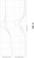
- dashed, solid, and dotted lines correspond to voltammetries with oxidation peaks of decreasing magnitude, respectively.
- the device can be configured to compress the increasing sum of background and effective I sens signals into recovered bumps of decreasing magnitude. This facilitates discrimination of both the analyte concentration and electrode kinetics. It also extends the dynamic range available over time to read out the information of interest.
- the multiple I sens generated by the multiple transducers are integrated by each sensor in the loop, and the resulting integrated voltage signals are converted again to current by the transconductors (905) and summed up together in this current domain.
- the resulting summed current signal is integrated in the integrating capacitor (904) of a second integrator stage.
- the sensing stage (100) comprises a FET sensor
- the interfacing stage (101) performs capacitive amplification through the passivation capacitance of the FET sensor and a feedback capacitance, and wherein unfiltered intramodulator feedback signals, the low-pass-filtered intramodulator feedback signals, and the unfiltered intermodulator feedback signals are current signals subtracted in current-mode to the delta error signal of the delta sigma modulators that comprise the device.
- the digital-to-analog conversion of all feedback signals is performed using current sources (901) controlled by d out (t).
- the capacitive amplification is performed by an amplifier (in this case a minimalistic implementation (906) comprising a current source and the metal-oxide-semiconductor (MOS) transistor of the FET sensor), the dielectric capacitance of the sensing membrane (902), and a feedback capacitor (903).
- the output voltage of the capacitive amplifier is connected to a transconductor (905) that converts it to a transconductor output current.
- the transconductor output current is integrated in the integrating capacitor (904) of a single-stage integrator.
- the controlled current source of the low-pass-filtered intramodulator feedback path can be implemented as depicted in figure 9B : using an ultra-low leakage MOS transistor operating with a selectable drain-source voltage via an e.g. multiplexer stage.
- the transistor can be biased to have a null drain-source voltage when the output of d out (t) is zero. It can also be biased to a null source-bulk voltages, which cause null conduction through the MOS transistor channel and the diffusion diodes, respectively, from the capacitive amplifier. While a non-zero d out (t) selects a non-zero drain-source voltage, this voltage (i.e. ⁇ V dout ) can be set in practice to be also very low and proportional to d out (t).
- the device of figures 9A and 9B can be configured to compress the increasing sum of drift and effective V sens signals into recovered bumps of amplitude proportional to the added rates. This facilitates discrimination of the effective V sens signal to detect in front of the drift, and identification of the chemical reactive rising the concentration of the analyte of interest. It also extends the dynamic range available over time in front of the sensor drift.
Landscapes
- Engineering & Computer Science (AREA)
- Theoretical Computer Science (AREA)
- Compression, Expansion, Code Conversion, And Decoders (AREA)
Abstract
A delta-sigma device that comprises transducers (2) and delta-sigma modulators (3) wherein the transducers (2) comprise: a sensing stage (100) that detect a property of the environment (106) and an interfacing stage (101); and the delta-sigma modulators (3) comprise: an input stage (113, 114), connected to the interfacing stages (101), for receiving an unfiltered intramodulator feedback signal (109) and a low-pass-filtered intramodulator feedback signal (110), and subtracting them from a sum of one or more of the input transduced signals (108) to obtain a delta error signal (111), a feedforward low-pass filtering stage (102); an analog-to-digital encoder (104), that converts the filtered delta error signal into a digital output signal dout(t) (112), an unfiltered intramodulator feedback path, that converts dout(t) (112) into the unfiltered intramodulator feedback signal (109), and a low-pass-filtered intramodulator feedback path, that converts dout(t) (112) into the low-pass-filtered intramodulator feedback signal (110).
Description
- The object of the present invention is a delta-sigma sensing device with background signal attenuation and distributed encoding.
- Sensor technologies play a critical role in various industries, including environmental monitoring, automotive, aerospace, medical, and consumer electronics. These sensors are designed to measure and monitor different physical (e.g., pressure, temperature, humidity) and chemical (e.g., analyte concentrations) parameters, providing essential data for a wide range of applications. To enable the sensors to communicate with other devices for performing further computation, the sensors are commonly "smartened" by incorporation of integrated circuits for processing the sensor signal and converting it into a digital format readable from external user devices.
- Achieving high precision and accuracy in smart sensing devices is often hampered by factors such as drift and offset. Drift refers to a slow, continuous change in the output of a sensor over time, independent of the input signal of interest. This can be attributed to aging, contamination of the sensing surface, and other environmental factors such as thermal, mechanical or electrical stress. Offset, on the other hand, is a constant component in the sensor output signal, regardless of the input value. It is usually caused by manufacturing imperfections or other external influences. Inaccurate measurements may lead to incorrect decision-making, reduced system efficiency, and, in some cases, critical failures.
- In practice, calibration of these two factors is frequently required for the sensing devices to perform within operational requirements. Calibration needs represent a key challenge to device autonomy together with energy consumption. A third aspect - miniaturization - adds to autonomy as crucial trait for enabling a ubiquitous usage of the devices. Recent advances to sensor technologies enable fabrication of physical and chemical sensors below the microscale. But, as the amplitude of the signals transduced decreases with size, downscaling accentuates the sensitivity to the aforementioned drift and offset effects.
- Different strategies have been described in the state of the art to compensate for drift: A common one, subtracting a cancellation term from the sensor output during a calibration phase, is not effective for monitoring along extended periods of time as drift varies due to environmental determinants. Other popular techniques, like using a threshold to differentiate between signal changes and drift rely on the signal being larger than drift, which may not always be the case. Performing a differential measurement from a reference sensor requires electrical matching and drift similarity between the two, which might not be feasible due to intrinsic manufacturing variability.
- Circuit methods proposed for removing or cancelling offset involve applying a bias at the device, reconfigured within a limited range during a separate calibration phase. The adoption of machine learning algorithms and artificial intelligence (Al) in sensor systems can also help to detect and compensate drift and offset. By analyzing historical sensor data and identifying patterns, these algorithms can predict and correct the resulting errors in real-time, leading to more accurate and reliable measurements. However, and due to their complexity, embedding Al models in a device generally translates into a substantial increase in its dimensions and energy budget.
- In this scenario, electrochemical microsensors fabricated in semiconductor technologies offer advantages such as miniaturization, mass fabrication, and ease of integration with CMOS circuits for embedding signal processing as smart sensing devices.
- Indeed, the amperometric sensor family shown in
figure 1 is particularly appealing since a simple three-microelectrode cell structure allows to evaluate redox reactions in solution at a target analyte potential (VRW) between reference (RE) and working (WE) electrodes. Under potentiostatic operation, that is ensuring a constant voltage at VRW and also null current through RE, the counter electrode (CE) supplies all the current needed for the electrochemical reaction at the surface of the WE. Thus, unwanted voltage drops of VRW at RE can be effectively avoided. - In this configuration, the electrode-electrolyte interface is usually modelled as the small-signal electrical circuit of
figure 1 , where isens is the CE-WE current change to be measured, while Rct, Cdl and Rs stand for the charge transfer resistance, the double layer capacitance and the electrolyte solution resistance, respectively. -
Figure 2 shows a field-effect transistor (FET) sensor easy to miniaturize and replicate as sensor array in semiconductor technologies. In standard CMOS technologies, the FET can be integrated as a metal-oxide-semiconductor transistor with the metal connection at the gate replaced by a liquid. The liquid contains the target analytes to be measured, which interact with the gate insulator functionalized as sensing surface. Changes in the analyte concentrations are transduced into a potential change at the gate insulator surface dependent upon the sensitivity to each analyte. These electrical variations in the gate potential can then be read out in the electrical domain by use of electronic circuits. - In the case of a FET electrochemical sensor fabricated in a standard CMOS technology, the FET can be modelled as the electrical circuit of
figure 2 , where Vsens is the potential change to be measured due to a variation in the chemical contribuent Vchem, while Csens stand for the sensing capacitance due to the dielectric sensing membrane. - Despite the aforementioned advantages, the practical usage of electrochemical microsensors is limited by phenomena like fouling and parasitic currents or trapped charges at the sensing surface (e.g., drifting and offset components). Such phenomena introduce variability between sensors and can severely impair the dynamic range and accuracy of transient measurements.
- Drift is particularly problematic for small signals and long-term measurements as it can be difficult to identify the signal amongst the shifting baseline. Together with offset components- and in the context of sensor readout, the sensor output can be driven outside of the analogue-to-digital converter input range and saturate. This also means an analogue-to-digital converter will need to cover a wide input range, which can increase quantization noise.
- Classic solutions to integrate the potentiostatic-amperometric readout in CMOS technologies employ potentiostat circuits based on operational amplifiers that enforce a negative feedback loop of the CE current in order to control VRW. The resulting sensor current can then be translated into voltage and converted to the digital domain through pulse-width or pulse-density modulators.
- Recent efforts have been directed to fusing both, the potentiostat and ADC functions, into a single circuit block using delta-sigma modulators. An interesting concept related with this scenario is what is known as sensor in the loop: reusing the sensor dynamics available shown in
figure 1 as feedforward filtering stage for quantization noise shaping inside a delta-sigma modulator with either discrete- or continuous-time feedback. Apart from the obvious advantage of circuit power and area savings, the reuse of the sensor as continuous-time feedforward filter automatically adapts its anti-aliasing cut-off frequency to the sensor intrinsic bandwidth. - In the case of field-effect-transistor (FET) sensors, the common approach is to use the transistor as a voltage follower. More recent circuits read out the device in current mode, which facilitates direct filtering and the use of delta-sigma modulation schemes alike to the ones previously described for amperometric sensors.
- On- and off-chip compensation methods have been proposed to overcome sensor offsets and drifts to some extent. However, none of the former approaches addresses, for instance, how to monitor in the long term under drift or offset interferents, which can have higher intensity than the signals of interest and may be influenced by evolving environmental factors. This is the case of commercial applications like environmental monitoring or wearable chemical sensing, in which the wide adoption of these analytical systems is still limited mainly due to sensor non-idealities, and due to the restricted deployability of these devices in terms of compactness and energy autonomy.
- The delta-sigma sensing device of the present invention has built-in adaptive pulse modulation encoding for delivering sensor biasing, analog-to-digital conversion, and attenuation of undesired background sensor signals (e.g., DC offset, drifts) lying out of the frequency band of interest.
- The device comprises one or more transducers and one or more delta-sigma modulators. Firstly, each of the transducers comprises a sensing stage intended to detect a property of the environment such as temperature, humidity, analyte concentrations, and to convert it into an electrical input signal. Each transducer also comprises an interfacing stage, connected to the sensing stage, that receives the electrical input signal and feeds it as input transduced signal to one or more of the delta-sigma modulators.
- Secondly, each of the delta-sigma modulators comprises an input stage, connected to the interfacing stage, for receiving an unfiltered intramodulator feedback signal and a low-pass-filtered intramodulator feedback signal, and subtracting them from a sum of one or more of the input transduced signals to obtain a delta error signal.
- Following the input stage, each modulator comprises a feedforward low-pass filtering stage, that obtains a filtered delta error signal, and an analog-to-digital encoder, following the feedforward filtering stage, that converts the filtered delta error signal into a digital output signal dout(t).
- Between the analog-to-digital encoder and the input stage, the modulator comprises an unfiltered intramodulator feedback path, that converts dout(t) into the unfiltered intramodulator feedback signal, and a low-pass-filtered intramodulator feedback path, between the analog-to-digital encoder and the input stage, that converts dout(t) into the low-pass-filtered intramodulator feedback signal.
- In front of the state of the art, the present invention offers:
- (i) tunable compression of interfering frequency components to increase the dynamic range, the readout resolution, and the energy efficiency; and
- (ii) distributed pulse modulation encoding, to increase the maximum overall encoder sampling rate and to effectively model dependencies between the input signals transduced by the sensors.
- To complement the description of the invention for a better understanding of its characteristics, and in accordance with a preferred example of practical embodiment thereof, a set of drawings is attached as an integral part of said description. The drawings represent, with illustrative and non-limiting character:
-
Figure 1 .- Shows the small-signal electrical model of the electrode-electrolyte interfaces for a three-electrode electrochemical cell of the state of the art. -
Figure 2 .- Shows the electrical model of a FET electrochemical sensor of the state of the art fabricated in a standard CMOS technology. -
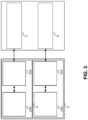
Figure 3 .- Shows a general schematic representation of a first example implementation of the device, in which each transducer is connected to a unique delta-sigma modulator. -
Figures 4A and4B .- Show a detailed schematic representation of a first example implementation of the device, in which each transducer is connected to a unique delta-sigma modulator. -
Figure 5 .- Shows a general schematic representation of a second example implementation of the device, in which one or more transducers are connected to one or more delta-sigma modulators. -
Figure 6 .- Shows a detailed schematic representation of a second example implementation of the device, in which one or more transducers are connected to one or more delta-sigma modulators. -
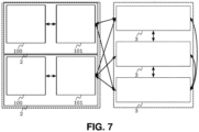
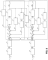
Figure 7 .- Shows a general schematic representation of a third example implementation of the device, in which some of the transducers are connected to more than one delta-sigma modulator, and wherein some of the outputs of the delta-sigma modulators are fed back to some of the other delta-sigma modulators that comprise the device. -
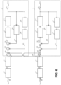
Figure 8 .- Shows a detailed schematic representation of a third example implementation of the device, in which some of the transducers are connected to more than one delta-sigma modulator, and wherein some of the outputs of the delta-sigma modulators are fed back to some of the other delta-sigma modulators that comprise the device. -
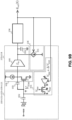
Figures 9A and9B .- Show a detailed schematic representation of the device implemented according to a first embodiment, in which a FET electrochemical transducer is connected to a delta-sigma modulator. -
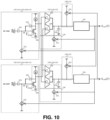
Figure 10 .- Shows a detailed schematic representation of the device implemented according to a second embodiment, in which one or more FET electrochemical transducers are connected to one or more delta-sigma modulators. -
Figure 11 .- Shows a detailed schematic representation of the device implemented according to a third embodiment, in which a three-electrode cell - operating as a potentiostatic-amperometric transducer - is connected to a delta-sigma modulator. -
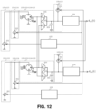
Figure 12 .- Shows a detailed schematic representation of the device implemented according to a fourth embodiment, in which one or more three-electrode cells, operating as a potentiostatic-amperometric transducers, are connected to one or more delta-sigma modulators. -
Figure 13 .- Shows the signal recovered after demodulating the transient response (bottom) of the first embodiment of the device to a prototypical increase in the analyte concentration causing a transition in the effective rate of Vsens under constant, and substantial, drift rate (top). -
Figure 14 .- Shows the signal recovered after demodulating the transient response (bottom) of the third embodiment of the device to an Isens in line with a prototypical half voltammetry cycle with large resistive losses at the working electrode-electrolyte interface (top). - It is described below, with the help of
figures 1 to 14 , a preferred embodiment of the delta-sigma device with background signal attenuation and distributed encoding, object of the present invention. - As presented in
figures 3 and5 , the delta-sigma device comprises one or more transducers (2) and one or more delta-sigma modulators (3). As shown in detail infigures 4A ,4B and6 , each of the transducers (2) comprises a sensing stage (100) intended to detect a property of the environment Xin1(t) (106) and configured to convert it into an electrical input signal (107), and an interfacing stage (101), connected to the sensing stage (100), that receives the electrical input signal (107) and feeds it as input transduced signals (108) to one (figures 4A ,4B ) or more (figure 6 ) of the delta-sigma modulators (3). - Moreover, each of the delta-sigma modulators (3) comprises, as shown in
figures 4A ,4B and6 , an input stage (113, 114), connected to the interfacing stages (101), for receiving an unfiltered intramodulator feedback signal (109) and a low-pass-filtered intramodulator feedback signal (110), and subtracting them from a sum of one (figures 4A ,4B ) or more (figure 6 ) input transduced signals (108) to obtain a delta error signal (111). - Following the input stage (113, 114), each modulator (3) comprises a feedforward low-pass filtering stage (102), configured to obtain a filtered delta error signal, an analog-to-digital encoder (104), following the feedforward filtering stage (102), that converts the filtered delta error signal into a digital output signal dout(t) (112), an unfiltered intramodulator feedback path, between the analog-to-digital encoder (104) and the input stage (113, 114) that converts dout(t) (112) into the unfiltered intramodulator feedback signal (109), and a low-pass-filtered intramodulator feedback path, between the analog-to-digital encoder (104) and the input stage (113, 114), that converts dout(t) (112) into the low-pass-filtered intramodulator feedback signal (110).
- In an aspect of the invention, shown in
figures 3 ,4A , and4B , each transducer (2) is connected to a unique delta-sigma modulator (3). - In an aspect of the invention, presented in
figures 5 and6 , each transducer (2) is connected to more than one delta-sigma modulators (3). - In an aspect of the invention, disclosed in
figures 7 and8 , the device comprises one or more transducers (2) and two or more delta-sigma modulators (3). In this case, the device additionally comprises a plurality of unfiltered intermodulator feedback paths, connected to dout(t) (112) of each delta-sigma modulator (3) and configured to convert dout(t) into a plurality of unfiltered intermodulator feedback signals (116). What is more, the device additionally comprises a subtracting stage (117) before the feedforward low-pass filtering stage (102) that receives the unfiltered intermodulator feedback signals (116) of each unfiltered intermodulator feedback path. - In an aspect of the invention, the unfiltered intramodulator feedback paths and/or the unfiltered intermodulator feedback paths comprise a digital-to-analog converter stage (105).
- In an aspect of the invention the low-pass-filtered intramodulator feedback paths comprise a feedback low-pass filtering stage (103) and a digital-to-analog converter stage (105).
- The digital-to-analog-converter stage (105) can be placed before or after the low-pass filter, as shown in
figure 4A andfigure 4B . - In an aspect of the invention, the feedforward low-pass filtering stage (102) and the feedback low-pass filtering stages (103) comprise one or more leaky or non-leaky integrator stages, each integrator stage being configured to integrate a respective input signal.
- Regarding this embodiment, the low-pass filtering stage can be implemented combining multiple feedback and feedforward loops in a backbone made of integrator stages cascaded in series. Negative feedback is used to connect integrator outputs to the inputs of same or previous integrator stages in order to regulate the gain and frequency response of the filter. Feedforward connects the output of each integrator stage to the input of next stages in order to compensate for phase and amplitude distortion introduced by the feedback mechanism.
- What is more, a leaky integrator is a stage that receives an input signal and generates an output signal by integrating a leaked signal over time. The leaked signal is obtained based on a dampening factor applied to reduce the amplitude of the input signal. A non-leaky integrator is a stage that receives an input signal and generates an output signal by integrating the input signal without any leakage or dampening.
- In an aspect of the invention, one or more of the leaky or non-leaky integrator stages of the feedforward filtering stage (102) comprises a circuit equivalent of the dynamic electrical response of the transducer (2).
- A small-signal circuit equivalent is a simplified representation of the dynamic response of a device that describes its electrical behavior under small-signal excitation. The small-signal circuit equivalent consists of a set of linear circuit elements, such as resistors, capacitors, and controlled sources, that are connected to model the device.
- In an aspect of the invention, the analog-to-digital encoder (104) of the delta-sigma modulators (3) comprises a one-bit synchronous or asynchronous quantizer.
- In an aspect of the invention, the analog-to-digital encoder (104) of the delta-sigma modulators (3) comprises a one-bit asynchronous quantizer and a pulse generator that convert the filtered delta error signal into a digital, pulsing signal dout(t) (113).
- In an aspect of the invention, the analog-to-digital encoders (104) of the delta-sigma modulators (3) comprise a three-level asynchronous quantizer and a bipolar pulse generator that convert the filtered delta error signal into a digital, bipolar pulsing signal dout(t) (113).
- Regarding the previously described embodiments, a one-bit asynchronous quantizer is a stage that converts a continuous or discrete signal into a "0" or "1" binary signal using a thresholding operation. A one-bit synchronous quantizer converts a continuous or discrete signal into a binary signal using a thresholding operation and a sampling clock. It maps the input signal to either "0" or "1" at regular intervals determined by the clock frequency. A three-level asynchronous quantizer converts a continuous or discrete signal into three output levels using a thresholding operation. A three-level synchronous quantizer converts a continuous or discrete signal into three output levels using a thresholding operation and a clock determining regular sampling intervals.
- Furthermore, a digital pulsing signal consists of a sequence of square wave electrical pulses, each occupying one of two discrete, binary levels of amplitude: "0" or "1". A bipolar pulsing signal consists of a sequence of square wave electrical pulses, each occupying one of three discrete levels of amplitude: positive, negative or zero.
- In an aspect of the invention, shown in
figures 11 and12 , the transducers (2) are three-electrode cells operating as a potentiostatic-amperometric sensor, wherein the unfiltered intramodulator feedback signals (109), the low-pass-filtered intramodulator feedback signals (110), and the unfiltered intermodulator feedback signals (116) are current signals subtracted in current-mode to the delta error signal (111) of the delta sigma modulators of the device. Each three-electrode cell also comprises a sensing stage (100) and an interfacing stage (101). - In all feedback signals of
figure 11 , the digital-to-analog conversion is performed using current sources (901) controlled by dout(t) or the output of the filtering stage (103). To allow programmable and miniaturized filtering of very low cut-off frequencies in a microchip, the low-pass filtering stage (103) of the filtered intramodulator feedback loop is implemented in the digital domain. To this end, an implementation of the low-pass filtering stage (103) can comprise a FIR (Finite Impulse Response) or IIR (Infinite Impulse Response) digital low-pass filter clocked at a frequency lower that the average quantization frequency of the pulse generated and higher than its cut-off frequency. In the case of asynchronous quantization, an implementation of the low-pass filtering stage can comprise an asynchronous counter stage, connected between dout(t) and the digital low-pass filter, that synchronizes dout(t) by accumulating its respective updates over a clock period of the digital filter. The sensed currents Isens are integrated by the sensor in the loop. - In
figure 14 , dashed, solid, and dotted lines correspond to voltammetries with oxidation peaks of decreasing magnitude, respectively. As seen infigure 14 (bottom), the device can be configured to compress the increasing sum of background and effective Isens signals into recovered bumps of decreasing magnitude. This facilitates discrimination of both the analyte concentration and electrode kinetics. It also extends the dynamic range available over time to read out the information of interest. - In
Figure 12 , the multiple Isens generated by the multiple transducers are integrated by each sensor in the loop, and the resulting integrated voltage signals are converted again to current by the transconductors (905) and summed up together in this current domain. The resulting summed current signal is integrated in the integrating capacitor (904) of a second integrator stage. - In an aspect of the invention, described in
figures 9 and10 , the sensing stage (100) comprises a FET sensor, and the interfacing stage (101) performs capacitive amplification through the passivation capacitance of the FET sensor and a feedback capacitance, and wherein unfiltered intramodulator feedback signals, the low-pass-filtered intramodulator feedback signals, and the unfiltered intermodulator feedback signals are current signals subtracted in current-mode to the delta error signal of the delta sigma modulators that comprise the device. - In
figures 9A ,9B , and10 , the digital-to-analog conversion of all feedback signals is performed using current sources (901) controlled by dout(t). The capacitive amplification is performed by an amplifier (in this case a minimalistic implementation (906) comprising a current source and the metal-oxide-semiconductor (MOS) transistor of the FET sensor), the dielectric capacitance of the sensing membrane (902), and a feedback capacitor (903). The output voltage of the capacitive amplifier is connected to a transconductor (905) that converts it to a transconductor output current. After current-mode subtraction of the unfiltered intramodulator signal and, optionally, the unfiltered intermodulator signal, the transconductor output current is integrated in the integrating capacitor (904) of a single-stage integrator. - To allow the configuration of very-low cut-off frequencies in a microchip, and to minimize the leakage at the gate of the MOS transistor, the controlled current source of the low-pass-filtered intramodulator feedback path can be implemented as depicted in
figure 9B : using an ultra-low leakage MOS transistor operating with a selectable drain-source voltage via an e.g. multiplexer stage. The transistor can be biased to have a null drain-source voltage when the output of dout(t) is zero. It can also be biased to a null source-bulk voltages, which cause null conduction through the MOS transistor channel and the diffusion diodes, respectively, from the capacitive amplifier. While a non-zero dout(t) selects a non-zero drain-source voltage, this voltage (i.e. ±ΔVdout) can be set in practice to be also very low and proportional to dout(t). - In
figure 13 , the solid line corresponds to an increase in the analyte concentration causing a similar effective Vsens rate than the drift Vsens rate; the dotted line corresponds to an increase in the analyte concentration causing an effective Vsens rate of approximately half the drift Vsens rate; the dashed line corresponds to an increase in the analyte concentration causing an effective Vsens rate of approximately double the drift Vsens rate. As seen infigure 13 (bottom), the device offigures 9A and9B can be configured to compress the increasing sum of drift and effective Vsens signals into recovered bumps of amplitude proportional to the added rates. This facilitates discrimination of the effective Vsens signal to detect in front of the drift, and identification of the chemical reactive rising the concentration of the analyte of interest. It also extends the dynamic range available over time in front of the sensor drift.
Claims (15)
- A delta-sigma device characterized in that it comprises one or more transducers (2) and one or more delta-sigma modulators (3) wherein each of the transducers (2) comprises:- a sensing stage (100) intended to detect a property of the environment Xin(t) (106) and configured to convert it into an electrical input signal (107), and- an interfacing stage (101), connected to the sensing stage (100), that receives the electrical input signal (107) and feeds it as input transduced signals (108) to one or more of the delta-sigma modulators (3),and wherein each of the delta-sigma modulators (3) comprises:- an input stage (113, 114), connected to the interfacing stages (101), for receiving an unfiltered intramodulator feedback signal (109) and a low-pass-filtered intramodulator feedback signal (110), and subtracting them from a sum of one or more of the input transduced signals (108) to obtain a delta error signal (111),- a feedforward low-pass filtering stage (102), following the input stage (113, 114), configured to obtain a filtered delta error signal;- an analog-to-digital encoder (104), following the feedforward filtering stage (102), that converts the filtered delta error signal into a digital output signal dout(t) (112),- an unfiltered intramodulator feedback path, that comprises a digital-to-analog converter stage (105) between the analog-to-digital encoder (104) and the input stage (113, 114), that converts dout(t) (112) into the unfiltered intramodulator feedback signal (109), and- a low-pass-filtered intramodulator feedback path that comprises a feedback low-pass filtering stage (103) and a digital-to-analog converter stage (105), between the analog-to-digital encoder (104) and the input stage (113, 114), that convert dout(t) (112) into the low-pass-filtered intramodulator feedback signal (110).
- The device of claim 1, wherein each transducer (2) is connected to a single delta-sigma modulator (3).
- The device of claim 1, wherein each transducer (2) is connected to more than one delta-sigma modulator (3).
- The device of claim 1, wherein it comprises one or more transducers (2) and two or more delta-sigma modulators (3), and wherein the device additionally comprises a plurality of unfiltered intermodulator feedback paths that comprise a digital-to-analog converter stage (105), connected to dout(t) (112) of each delta-sigma modulator (3) and configured to convert dout(t) into a plurality of unfiltered intermodulator feedback signals (116), and wherein the device additionally comprises a subtracting stage (117) before the feedforward low-pass filtering stage (102) that receives the unfiltered intermodulator feedback signals (116) of each unfiltered intermodulator feedback path.
- The device of claims 1, wherein the feedforward low-pass filtering stage (102) or the feedback low-pass filtering stages (103) comprise one or more leaky or non-leaky integrator stages, each integrator stage being configured to integrate a respective input signal.
- The device of claim 5, wherein one or more of the leaky or non-leaky integrator stages of the feedforward filtering stage (102) comprises a circuit equivalent of the dynamic electrical response of the transducer (2).
- The device of claim 1, wherein the analog-to-digital encoder (104) of the delta-sigma modulators (3) comprises a one-bit synchronous or asynchronous quantizer.
- The device of claim 1, wherein the analog-to-digital encoder (104) of the delta-sigma modulators (3) comprises a one-bit asynchronous quantizer and a pulse generator that convert the filtered delta error signal into a digital, pulsing signal dout(t) (113) with a quantization frequency.
- The device of claim 8, wherein the low-pass filtering stage (103) additionally comprises a FIR (Finite Impulse Response) or IIR (Infinite Impulse Response) digital low-pass filter clocked at a frequency lower that the average of the quantization frequency and higher than its cut-off frequency.
- The device of claim 9, wherein the low-pass filtering stage (103) additionally comprises an asynchronous counter stage, connected between dout(t) and the digital low-pass filter, for synchronizing dout(t).
- The device of claim 1, wherein the analog-to-digital encoders (104) of the delta-sigma modulators (3) comprise a three-level asynchronous quantizer and a bipolar pulse generator that convert the filtered delta error signal into a digital, bipolar pulsing signal dout(t) (113).
- The device of claim 1, wherein the transducers (2) are three-electrode cells operating as a potentiostatic-amperometric sensor, and wherein the unfiltered intramodulator feedback signals, the low-pass-filtered intramodulator feedback signals, and the unfiltered intermodulator feedback signals are current signals subtracted in current-mode to the delta error signal (111).
- The device of claim 12, wherein the digital-to-analog converter stage (105) comprises current sources (901) controlled by dout(t) or the output of the filtering stage (103).
- The device of claim 13, wherein the controlled current sources (901) comprise an ultra-low leakage MOS transistor operating with a selectable drain-source voltage.
- The device of claim 1, wherein the sensing stage (100) comprises a FET sensor, and the interfacing stage (101) performs capacitive amplification through the passivation capacitance of the FET sensor and a feedback capacitance, and wherein unfiltered intramodulator feedback signals (109), the low-pass-filtered intramodulator feedback signals (110), and the unfiltered intermodulator feedback signals (116) are current signals subtracted in current-mode to the delta error signal (111).
Priority Applications (3)
| Application Number | Priority Date | Filing Date | Title |
|---|---|---|---|
| EP23382470.5A EP4465538A1 (en) | 2023-05-19 | 2023-05-19 | Delta-sigma sensing device |
| CN202480044917.3A CN121444352A (en) | 2023-05-19 | 2024-05-20 | DELTA-SIGMA Sensing Devices |
| PCT/EP2024/063866 WO2024240721A1 (en) | 2023-05-19 | 2024-05-20 | Delta-sigma sensing device |
Applications Claiming Priority (1)
| Application Number | Priority Date | Filing Date | Title |
|---|---|---|---|
| EP23382470.5A EP4465538A1 (en) | 2023-05-19 | 2023-05-19 | Delta-sigma sensing device |
Publications (1)
| Publication Number | Publication Date |
|---|---|
| EP4465538A1 true EP4465538A1 (en) | 2024-11-20 |
Family
ID=86497950
Family Applications (1)
| Application Number | Title | Priority Date | Filing Date |
|---|---|---|---|
| EP23382470.5A Pending EP4465538A1 (en) | 2023-05-19 | 2023-05-19 | Delta-sigma sensing device |
Country Status (3)
| Country | Link |
|---|---|
| EP (1) | EP4465538A1 (en) |
| CN (1) | CN121444352A (en) |
| WO (1) | WO2024240721A1 (en) |
Citations (1)
| Publication number | Priority date | Publication date | Assignee | Title |
|---|---|---|---|---|
| US11632118B2 (en) * | 2020-05-26 | 2023-04-18 | Melexis Technologies Nv | Closed-loop oscillator based sensor interface circuit |
-
2023
- 2023-05-19 EP EP23382470.5A patent/EP4465538A1/en active Pending
-
2024
- 2024-05-20 CN CN202480044917.3A patent/CN121444352A/en active Pending
- 2024-05-20 WO PCT/EP2024/063866 patent/WO2024240721A1/en not_active Ceased
Patent Citations (1)
| Publication number | Priority date | Publication date | Assignee | Title |
|---|---|---|---|---|
| US11632118B2 (en) * | 2020-05-26 | 2023-04-18 | Melexis Technologies Nv | Closed-loop oscillator based sensor interface circuit |
Non-Patent Citations (2)
| Title |
|---|
| AYMERICH JOAN ET AL: "A 15-[mu]W 105-dB 1.8-Vpp Potentiostatic Delta-Sigma Modulator for Wearable Electrochemical Transducers in 65-nm CMOS Technology", IEEE ACCESS, IEEE, USA, vol. 8, 30 March 2020 (2020-03-30), pages 62127 - 62136, XP011782982, DOI: 10.1109/ACCESS.2020.2984177 * |
| LI SHAOLAN ET AL: "A 174.3-dB FoM VCO-Based CT $\Delta \Sigma $ Modulator With a Fully-Digital Phase Extended Quantizer and Tri-Level Resistor DAC in 130-nm CMOS", IEEE JOURNAL OF SOLID-STATE CIRCUITS, IEEE, USA, vol. 52, no. 7, July 2017 (2017-07-01), pages 1940 - 1952, XP011654150, ISSN: 0018-9200, [retrieved on 20170623], DOI: 10.1109/JSSC.2017.2693244 * |
Also Published As
| Publication number | Publication date |
|---|---|
| WO2024240721A1 (en) | 2024-11-28 |
| CN121444352A (en) | 2026-01-30 |
Similar Documents
| Publication | Publication Date | Title |
|---|---|---|
| Ying et al. | Current sensing front-ends: A review and design guidance | |
| US9438261B2 (en) | Capacitance-to-digital converter and method for providing a digital output signal | |
| US20220221420A1 (en) | Methods and systems for readout of nanogap sensors | |
| CN103399201B (en) | A General Detection Chip System for Weak Signals of Sensors | |
| Nizza et al. | A low-power interface for capacitive sensors with PWM output and intrinsic low pass characteristic | |
| US11320468B2 (en) | Wide dynamic range current measurement front-end | |
| Georgakopoulou et al. | A capacitive-to-digital converter with automatic range adaptation for readout instrumentation | |
| CN215415186U (en) | Detection circuit based on four-electrode electrochemical gas sensor | |
| Mochizuki et al. | A high-accuracy high-speed signal processing circuit of differential-capacitance transducers | |
| Yin et al. | A compact low-power current-to-digital readout circuit for amperometric electrochemical sensors | |
| Chen et al. | A high dynamic range CMOS readout chip for electrochemical sensors | |
| WO2024240721A1 (en) | Delta-sigma sensing device | |
| Margarit-Taulé et al. | Delta-sigma sensing device | |
| Pol et al. | A femto-ampere sensitive direct-interface current-input sigma delta ADC for amperometric bio-sensor signal acquisition | |
| Cuenca-Michans et al. | A low-power neuromorphic CMOS delta-sigma modulator featuring tunable background attenuation and potentiostatic asynchronous readout for smart amperometric electrochemical sensors | |
| Zhang et al. | A 0.72 nW, 1 sample/s fully integrated pH sensor with 65.8 LSB/pH sensitivity | |
| Ghoreishizadeh et al. | Sub-mW reconfigurable interface IC for electrochemical sensing | |
| Aiassa et al. | New measurement method in drug sensing by direct total-charge detection in voltammetry | |
| US20240377353A1 (en) | Circuitry for measurement of electrochemical cells | |
| Ayub et al. | A 77.8-dB DR, 114.2 fJ/Step Amplifier-Less Current-to-Digital Converter | |
| Nawito et al. | A programmable energy efficient readout chip for a multiparameter highly integrated implantable biosensor system | |
| CN115580287A (en) | A Reconfigurable Sensor Interface Circuit Based on Switched Capacitor | |
| US12592710B2 (en) | Circuitry for measurement of electrochemical cells | |
| Asgari | Fully-Integrated CMOS pH, Electrical Conductivity, And Temperature Sensing System | |
| US20250244285A1 (en) | Circuitry for Measurement of Electrochemical Cells |
Legal Events
| Date | Code | Title | Description |
|---|---|---|---|
| PUAI | Public reference made under article 153(3) epc to a published international application that has entered the european phase |
Free format text: ORIGINAL CODE: 0009012 |
|
| STAA | Information on the status of an ep patent application or granted ep patent |
Free format text: STATUS: THE APPLICATION HAS BEEN PUBLISHED |
|
| AK | Designated contracting states |
Kind code of ref document: A1 Designated state(s): AL AT BE BG CH CY CZ DE DK EE ES FI FR GB GR HR HU IE IS IT LI LT LU LV MC ME MK MT NL NO PL PT RO RS SE SI SK SM TR |
|
| STAA | Information on the status of an ep patent application or granted ep patent |
Free format text: STATUS: REQUEST FOR EXAMINATION WAS MADE |
|
| 17P | Request for examination filed |
Effective date: 20250520 |