EP4465010A1 - Method and system for characterization of a photonic circuit - Google Patents
Method and system for characterization of a photonic circuit Download PDFInfo
- Publication number
- EP4465010A1 EP4465010A1 EP23315204.0A EP23315204A EP4465010A1 EP 4465010 A1 EP4465010 A1 EP 4465010A1 EP 23315204 A EP23315204 A EP 23315204A EP 4465010 A1 EP4465010 A1 EP 4465010A1
- Authority
- EP
- European Patent Office
- Prior art keywords
- component
- photonic circuit
- machine
- model
- characteristic value
- Prior art date
- Legal status (The legal status is an assumption and is not a legal conclusion. Google has not performed a legal analysis and makes no representation as to the accuracy of the status listed.)
- Withdrawn
Links
Images



Classifications
-
- G—PHYSICS
- G01—MEASURING; TESTING
- G01M—TESTING STATIC OR DYNAMIC BALANCE OF MACHINES OR STRUCTURES; TESTING OF STRUCTURES OR APPARATUS, NOT OTHERWISE PROVIDED FOR
- G01M11/00—Testing of optical apparatus; Testing structures by optical methods not otherwise provided for
-
- G—PHYSICS
- G06—COMPUTING OR CALCULATING; COUNTING
- G06N—COMPUTING ARRANGEMENTS BASED ON SPECIFIC COMPUTATIONAL MODELS
- G06N3/00—Computing arrangements based on biological models
- G06N3/02—Neural networks
- G06N3/06—Physical realisation, i.e. hardware implementation of neural networks, neurons or parts of neurons
- G06N3/067—Physical realisation, i.e. hardware implementation of neural networks, neurons or parts of neurons using optical means
- G06N3/0675—Physical realisation, i.e. hardware implementation of neural networks, neurons or parts of neurons using optical means using electro-optical, acousto-optical or opto-electronic means
-
- G—PHYSICS
- G06—COMPUTING OR CALCULATING; COUNTING
- G06N—COMPUTING ARRANGEMENTS BASED ON SPECIFIC COMPUTATIONAL MODELS
- G06N3/00—Computing arrangements based on biological models
- G06N3/02—Neural networks
- G06N3/08—Learning methods
- G06N3/084—Backpropagation, e.g. using gradient descent
-
- G—PHYSICS
- G06—COMPUTING OR CALCULATING; COUNTING
- G06N—COMPUTING ARRANGEMENTS BASED ON SPECIFIC COMPUTATIONAL MODELS
- G06N3/00—Computing arrangements based on biological models
- G06N3/02—Neural networks
- G06N3/08—Learning methods
- G06N3/09—Supervised learning
-
- G—PHYSICS
- G06—COMPUTING OR CALCULATING; COUNTING
- G06N—COMPUTING ARRANGEMENTS BASED ON SPECIFIC COMPUTATIONAL MODELS
- G06N10/00—Quantum computing, i.e. information processing based on quantum-mechanical phenomena
- G06N10/40—Physical realisations or architectures of quantum processors or components for manipulating qubits, e.g. qubit coupling or qubit control
Definitions
- the invention concerns a method for the characterizing of a photonic circuit and a system for implementing this method.
- Photonic circuits enable stable and compact light manipulation.
- quantum light for circuit-based quantum communications (e.g. quantum key distribution), quantum information processing, boson sampling and quantum simulation. See for example Wang al., Integrated photonic quantum technologies, Nat. Photonics 14, 273-284 (2020 ).
- Photonic circuits can have imperfections, such as crosstalk between components, imperfections in the directional couplers reflectivities, relative output losses, etc.
- the aim of the invention is to provide an improved method for characterizing photonic circuits, in particular for quantum applications.
- the invention concerns a method for characterization of a photonic circuit, comprising:
- imperfections on photonic circuits (10) can be mitigated.
- the machine-learning process can estimate appropriate values for the physical imperfections to compensate for their detrimental impact.
- such a method may incorporate one or several of the following features:
- the invention also concerns a system (1) for characterization of a photonic circuit (10) according to the above method.
- the system comprises:
- such a system may incorporate one or several of the following features:
- each component acting on light is separately identified and localized.
- a circuit (10) is said to be reconfigurable, if at least one of its components can modify its effect on light.
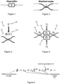
- Figure 1 shows a first example of component: a phase shifter applies a phase shift ⁇ on the incoming light.
- Figure 2 shows a second example of component: a directional coupler combines and splits incoming light. It is parametrized by its reflectivity R, which determines how the component reflects light.
- phase shift ⁇ value depends on the voltage V applied.
- the discrete photonic circuit (10) comprises at least one reconfigurable component (12).
- the circuit (10) generally has a higher number of reconfigurable components (12), as in Figure 7 . Indeed, it would not be very interesting to implement the method just for one or two reconfigurable components (12), as in Figures 3 and 4 , but it is covered by the scope of the invention.
- Figure 3 shows a first example of photonic circuit (10), composed of just one reconfigurable component (12), more precisely a reconfigurable directional coupler, that is a directional coupler whose reflectivity R can be controlled by applying voltage V.
- FIG. 4 shows a second example of photonic circuit (10), composed of:
- Each component (12, 14) is modelled by a set of characteristic values (CV), that is one or several characteristic values (CV).
- CV characteristic values
- Figure 5 shows an example of characteristic value (CV) for a reconfigurable component (12): the phase-voltage relation of a thermo-optic phase shifter.
- Figure 6 shows an example of characteristic value (CV) for a fixed component (14): the reflectivity R of the directional coupler, which determines how much light is sent into each direction.
- the photonic circuit (10) itself can also be described by characteristic values (CV). For instance:
- RDSP Reconfigurable Discrete-Scheme Photonic
- This special RSDP comprises:
- Figure 7 shows such a RSDP circuit (10), comprising 122 phase shifters (12), that are the small rectangles, and 132 directional couplers (14), that are the crossings with a horizontal line.
- the light travels along the lines, from one side to the other side of the circuit (10), for example left to right.
- the invention can be used for the mitigation of imperfections on RDSP circuits (10). Such imperfections comprise crosstalk between components (12, 14) of the circuit (10), imperfections in the directional couplers reflectivities, relative output losses, etc.
- Figure 8 illustrates crosstalk between thermal phase shifters.
- crosstalk prevents precise light manipulation and reduces the fidelity of the operations.
- Figure 9 illustrates imperfections in directional coupler reflectivities. Fabrication errors introduce statistical errors ⁇ in the reflectivities of the couplers across the circuit. Systematic errors r arise when the light's wavelength is shifted. These imperfections severely limit the range of transformations that can be operated on light with the circuit.
- FIG 10 illustrates relative output losses of the circuit.
- the circuit output ports do not transmit the same number of photons relative to each other. Its impact and mitigation are not well understood in the literature for now.
- a crucial point for mitigating phase shifter crosstalk, directional coupler reflectivity imperfections or relative output losses, is to know the characteristic values (CV) of the components (12, 14) and the circuit (10).
- the method according to the invention recovers the characteristic values (CV) using machine-learning.
- Figure 11 is a flowchart illustrating the method according to the invention, for the characterization of a photonic circuit (10).
- the process starts with a coarse component-wise characterization of the circuit (10). If done, it can be used to determine the form of the phase-shifter phase-voltage relation and also to give the machine-learning model a good initial state when it starts learning.
- the process starts without component-wise characterization.
- the machine-learning model is initialized with specific or random values.
- step (B) we proceed by acquiring data samples (DS) on the circuit (10).
- step (C) these data samples (DS) are given to our machine-learning model, which is trained to replicate them.
- step (D) when the learning process is finished, the values for the parameters of interest are extracted from the model.
- Figure 12 illustrates the experimental system (1) used to carry out the characterization method according to the invention.
- System (1) comprises:
- the continuous-wave laser is injected into the circuit (10) to characterize.
- the output laser power is monitored by the powermeter array (30).
- the optional optical switch (50) allows to address automatically different circuit inputs.
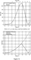
- Figure 13 shows two graphs illustrating an example of initial step (A), including a component-wise characterization substep.
- phase shifter is characterized separately from the others.
- the voltage V is swept from zero to a maximum voltage chosen by the operator.
- the interference fringe is recorded on the powermeters (left graph). From the fringe data, we can compute the phase shift ⁇ as a function of the voltage V applied (right graph).
- machine-learning denotes computer science methods where a program extrapolates information from a given set of data.
- the samples are of the form:
- the voltages V applied on all the phase shifters are set to random values.
- the list of input ports specifies into which input ports light is injected to acquire this particular sample (DS).
- the set of input ports to address is chosen such that every directional coupler and phase shifter to characterize encounters light at least once.
- the number of data samples (DS) should be equally divided among the input ports. It is not necessary to change the input port for each new sample (DS): all samples associated to an input port can be acquired in one run.
- Figure 14 shows a flowchart illustrating an example of machine-learning step (C), wherein the machine-learning model is used to characterize a photonic circuit (10).
- Parameters marked with asterisks represent characteristic values (CV) to learn.
- the model takes as input a list of voltages V that are applied on the circuit phase shifters.
- the form of the phase-voltage relation is chosen by the operator based on their knowledge of the components or after the component-wise characterization of step (A).
- the model predicts the phases ⁇ applied physically on the circuit (10), which are then passed to a simulation of the circuit (10), along the parameters R and T , the column vectors containing the reflectivities and output port transmissions.
- the model then outputs the corresponding list of laser powers (normalized such that it sums to 1).
- the characteristic values (CV) marked with asterisks are directly accessible.
- Figure 15 illustrates the machine-learning step (C) including the repetition of two substeps: training and testing.
- the model is evaluated on the training samples and its parameters (phase-voltage relation, DC reflectivities, output losses) are evolved using standard backpropagation, such that the difference between the model predictions and the samples is minimized.
- the testing substep the model is evaluated on the testing samples to monitor if the model is overfitting.
- Figure 16 shows a flowchart illustrating the extraction step (D). Due to the nature of the machine-learning model, the estimated characteristic values (CV) can be simply extracted and directly used for the intended application.
- phase-voltage relation After having trained the machine-learning model, we extract the phase-voltage relation and use it to implement 300 randomly chosen phase configurations. We compare the resulting power distributions with theoretical predictions. The average difference is only 3 %.
Landscapes
- Engineering & Computer Science (AREA)
- Physics & Mathematics (AREA)
- Theoretical Computer Science (AREA)
- General Physics & Mathematics (AREA)
- Biomedical Technology (AREA)
- Biophysics (AREA)
- Health & Medical Sciences (AREA)
- Life Sciences & Earth Sciences (AREA)
- Molecular Biology (AREA)
- Artificial Intelligence (AREA)
- Evolutionary Computation (AREA)
- General Health & Medical Sciences (AREA)
- Computational Linguistics (AREA)
- Computing Systems (AREA)
- General Engineering & Computer Science (AREA)
- Data Mining & Analysis (AREA)
- Mathematical Physics (AREA)
- Software Systems (AREA)
- Neurology (AREA)
- Chemical & Material Sciences (AREA)
- Analytical Chemistry (AREA)
- Semiconductor Lasers (AREA)
Abstract
The invention concerns a method for characterization of a photonic circuit, comprising: an initial step (A), wherein the photonic circuit is provided, comprising at least one reconfigurable component to characterize and possibly at least one fixed component, each reconfigurable component being associated with at least one control parameter, each component being modelled by at least one characteristic value; an acquisition step (B), wherein data samples (DS) are acquired from measurements of at least one measurable output quantity on the photonic circuit; a machine-learning step (C), wherein the data samples (DS) are used in a machine-learning model, that determines a relation between: 1. the control parameter(s) of the reconfigurable component(s), 2. the characteristic value(s) of the fixed or reconfigurable component(s), and 3. the effect(s) of the component(s) on the measurable output quantity(ies); and possibly other characteristic value(s) of the photonic circuit; and an extraction step (D), wherein characteristic value(s) are extracted, based on results of the machine-learning step (C). The invention also concerns a system for implementing such a method.
Description
- The invention concerns a method for the characterizing of a photonic circuit and a system for implementing this method.
- Photonic circuits enable stable and compact light manipulation.
- They are used with classical light for communications, sensing and broadband analogue signal processing. See for example Bogaerts et al., Programmable photonic circuits, Nature 586, 207-216 (2020).
- They are also used with quantum light for circuit-based quantum communications (e.g. quantum key distribution), quantum information processing, boson sampling and quantum simulation. See for example Wang al., Integrated photonic quantum technologies, Nat. Photonics 14, 273-284 (2020).
- Photonic circuits can have imperfections, such as crosstalk between components, imperfections in the directional couplers reflectivities, relative output losses, etc.
- While manufacturers make efforts to reduce the amount of crosstalk by physical means (e.g. trenches around phase shifters to prevent heat diffusion), as the circuits grow in size and complexity while becoming more compact, there is a need for crosstalk characterization/calibration and compensation methods.
- The aim of the invention is to provide an improved method for characterizing photonic circuits, in particular for quantum applications.
- To this end, the invention concerns a method for characterization of a photonic circuit, comprising:
- an initial step (A), wherein the photonic circuit (10) is provided, comprising at least one reconfigurable component (12) to characterize and possibly at least one fixed component (14), each reconfigurable component (12) being associated with at least one control parameter (CP), each component (12, 14) being modelled by at least one characteristic value (CV);
- an acquisition step (B), wherein data samples (DS) are acquired from measurements of at least one measurable output quantity on the photonic circuit (10) ;
- a machine-learning step (C), wherein the data samples (DS) are used in a machine-learning model, that determines:
- a relation between:
- 1. the control parameter(s) (CP) of the reconfigurable component(s) (12),
- 2. the characteristic value(s) (CV) of the fixed or reconfigurable component(s) (12, 14), and
- 3. the effect(s) of the component(s) (12, 14) on the measurable output quantity(ies); and
- possibly other characteristic value(s) (CV) of the photonic circuit (10); and
- a relation between:
- an extraction step (D), wherein characteristic value(s) (CV) are extracted, based on results of the machine-learning step (C).
- Thanks to the invention, imperfections on photonic circuits (10) can be mitigated. The machine-learning process can estimate appropriate values for the physical imperfections to compensate for their detrimental impact.
- According to further aspects of the invention which are advantageous but not compulsory, such a method may incorporate one or several of the following features:
- The method can comprise a component-wise characterization substep, wherein individual characterization(s) (IC) of at least one of the component(s) (12, 14) is performed. In the machine-learning step (C), the individual characterization(s) (IC) and the data samples (DS) can then be used in the machine-learning model. The component-wise characterization substep is optional. If the component-wise characterization substep is not performed, the machine-learning model is initialized with specific or random initial characteristic values (CV).
- The reconfigurable component(s) (12) of the photonic circuit (10) can comprise at least one phase shifter. In the component-wise characterization substep, the individual characterization (IC) of the phase shifter can be performed as a relation between phase and a control parameter (CP), such as voltage or current.
- The fixed component(s) (14) of the photonic circuit (10) can comprise at least one directional coupler. In the component-wise characterization substep, the individual characterization of the directional coupler can be an estimation of a characteristic value, such as reflectivity.
- The discrete photonic circuit (10) can comprise phase shifters, directional couplers, or any other discrete optical component.
- The photonic circuit (10) can be free-space or integrated on a chip.
- The model can be coded in Python using the PyTorch package, or any other suitable machine-learning framework in any programming language.
- The characteristic values (CV) can be imperfections, including crosstalk between reconfigurable components, directional coupler reflectivities differing from target values, unbalanced input and/or output losses of the circuit.
- In the acquisition step (B), among the data samples (DS), each individual data sample can include an input configuration, comprising a list of one or several input port(s) used to input light in the photonic circuit (10) for this specific data sample (DS).
- In the acquisition step (B), among the data samples (DS), each individual data sample can include a set of values corresponding to the or each control parameter (CP) of the reconfigurable component(s) (12), such as voltage or current.
- In the acquisition step (B), among the data samples (DS), each individual data sample can include at least one measurable output quantity of the photonic circuit (10), such as single-photon counts, coincidence rates, laser power. The coincidence rates relate to the simultaneous single-photon detection on multiple detectors.
- In the acquisition step (B), the data samples can be separated into at least two distinct datasets : training samples, which are used to update the state of the machine-learning model; and test samples, which are used to monitor overfitting of the model on the training samples, by comparing predictions of the model with data not previously seen by the model.
- The machine-learning step (C) can comprise a training sub-step, wherein the data samples (DS) are evolved using standard backpropagation, such that a difference between model predictions and the data samples (DS) is minimized.
- The machine-learning step (C) can comprise a testing sub-step, configured to monitor if the model is overfitting, that is the model is trained too well on a dataset of training samples, to the point that the model becomes too specialized and loses its ability to generalize to unseen data. The model is evaluated on the testing samples to monitor if the model is overfitting.
- The machine-learning model can comprise a mathematical relation linking the control parameter(s) (CP) of the reconfigurable component(s) (12) to their physical effect(s), such as voltage to optical phase shift for thermo-optics phase shifters. The model can store the characteristic value(s) (CV) of the component(s) (12, 14) and other characteristic value(s) (CV) of the photonic circuit (10). The model can optimize the mathematical relation and the characteristic value(s) (CV) of the fixed components (14) and of the photonic circuit (10), during the machine-learning step (C) to replicate the data samples (DS).
- The mathematical relation can be a matrix relation.
- In the extraction step (D), characteristic value(s) (CV) of the photonic circuit (10), and in particular imperfections of the photonic circuit (10), can be extracted from the machine-learning model. In this embodiment, these characteristic values are the final results of the method.
- The extraction step (D) can be followed by a correction step, wherein the photonic circuit (10) receives a calibration mitigating imperfections and implementing accurate operations.
- The invention also concerns a system (1) for characterization of a photonic circuit (10) according to the above method. The system comprises:
- the photonic circuit (10), comprising at least one reconfigurable component (12) and possibly at least one fixed component (14);
- at least one light source (20) positioned at the input of the photonic circuit (10);
- a detection device (30) positioned at the output of the photonic circuit (10);
- a computer unit (40), provided with a machine-learning model.
- According to further aspects of the invention which are advantageous but not compulsory, such a system may incorporate one or several of the following features:
- The photonic circuit (10) can be a reconfigurable discrete-scheme photonic chip.
- The light source (20) can be a continuous-wave laser.
- The detection device (30) can be a powermeter array.
- The computer unit (40) can be a CPU, GPU, QPU, TPU, or any suitable unit.
- The system can comprise an optical switch (50) positioned between the light source (20) and the photonic circuit (10), the optical switch (50) being configured to automatically address different inputs of the photonic circuit (10).
- The system can be constructed as a quantum computer.
- The invention will now be explained in correspondence with the annexed figures, and as an illustrative example, without restricting the object of the invention. In the annexed figures:
-
Figure 1 is a schematic representation of a component, more precisely a phase shifter. -
Figure 2 is a schematic representation of another component, more precisely a directional coupler. -
Figure 3 is a schematic representation of a photonic circuit, composed of a reconfigurable directional coupler. -
Figure 4 is a schematic representation of another photonic circuit, composed of two reconfigurable phase shifter and two fixed directional couplers. -
Figure 5 is an equation showing characteristic values of a reconfigurable phase shifter. -
Figure 6 is a schematic representation of a directional coupler, showing its characteristic value of reflectivity. -
Figure 7 is a schematic representation of a photonic circuit, comprising many phase shifters and directional couplers. -
Figure 8 is a schematic representation of crosstalk between directional couplers. -
Figure 9 is a schematic representation of imperfection of a directional coupler. -
Figure 10 is a schematic representation of output losses of a photonic circuit. -
Figure 11 is a flowchart of the method according to the invention. -
Figure 12 is a schematic representation of a system designed for implementing the method according to the invention. -
Figure 13 is a set of two graphs illustrating a component-wise characterization substep. -
Figure 14 is a flowchart illustrating a machine-learning step. -
Figure 15 is a diagram illustrating two substeps of training and testing of the machine-learning step. -
Figure 16 is a flowchart similar toFigure 14 and illustrating the extraction step. - In a discrete-scheme photonic circuit (10), each component acting on light is separately identified and localized. A circuit (10) is said to be reconfigurable, if at least one of its components can modify its effect on light.
-
Figure 1 shows a first example of component: a phase shifter applies a phase shift Φ on the incoming light. -
Figure 2 shows a second example of component: a directional coupler combines and splits incoming light. It is parametrized by its reflectivity R, which determines how the component reflects light. - We divide the components of the circuit (10) into two categories:
- Reconfigurable components (12), which can modify their action on light.
- Fixed components (14), which can not modify their action on light.
- The state of reconfigurable components (12) is controlled by control parameters (CP). For example, for thermal phase shifters, the phase shift Φ value depends on the voltage V applied.
- Within the scope of the invention, the discrete photonic circuit (10) comprises at least one reconfigurable component (12). In practice, the circuit (10) generally has a higher number of reconfigurable components (12), as in
Figure 7 . Indeed, it would not be very interesting to implement the method just for one or two reconfigurable components (12), as inFigures 3 and 4 , but it is covered by the scope of the invention. -
Figure 3 shows a first example of photonic circuit (10), composed of just one reconfigurable component (12), more precisely a reconfigurable directional coupler, that is a directional coupler whose reflectivity R can be controlled by applying voltage V. -
Figure 4 shows a second example of photonic circuit (10), composed of: - two reconfigurable components (12), more precisely two reconfigurable phase shifters controlled by voltages V1 and V2 respectively, and
- two fixed components (14), more precisely two fixed directional couplers of reflectivity R1 and R2.
- Each component (12, 14) is modelled by a set of characteristic values (CV), that is one or several characteristic values (CV).
-
Figure 5 shows an example of characteristic value (CV) for a reconfigurable component (12): the phase-voltage relation of a thermo-optic phase shifter. -
Figure 6 shows an example of characteristic value (CV) for a fixed component (14): the reflectivity R of the directional coupler, which determines how much light is sent into each direction. - The photonic circuit (10) itself can also be described by characteristic values (CV). For instance:
- Relative output transmissions
- Relative input transmissions
- We consider a special case of a Reconfigurable Discrete-Scheme Photonic (RDSP) circuit (10), that is a circuit whose components can be phase shifters and beamsplitters, which can be fixed or not.
- This special RSDP comprises:
- reconfigurable phase shifters controlled by voltage V: the characteristic values (CV) are the coefficients in the phase-voltage relation of individual components,
- fixed directional couplers: the characteristic values (CV) are the reflectivities R of individual components;
- relative output losses are the characteristic values (CV) of the circuit (10) itself.
-
Figure 7 shows such a RSDP circuit (10), comprising 122 phase shifters (12), that are the small rectangles, and 132 directional couplers (14), that are the crossings with a horizontal line. The light travels along the lines, from one side to the other side of the circuit (10), for example left to right. - The invention can be used for the mitigation of imperfections on RDSP circuits (10). Such imperfections comprise crosstalk between components (12, 14) of the circuit (10), imperfections in the directional couplers reflectivities, relative output losses, etc.
-
Figure 8 illustrates crosstalk between thermal phase shifters. - Regardless of the technology enabling reconfigurability (thermal, mechanical, electrical...), crosstalk is to be expected. Crosstalk prevents precise light manipulation and reduces the fidelity of the operations.
- For the mitigation of this imperfection, we assume that the phase-voltage relation governing the behaviour of the phase shifters is of the general form:

- V is the column vector containing all applied voltages V,
- .k represents element-wise exponentiation,
- C 0 is a vector,
- and C k□1 are matrices.
- The physical interpretation of this formula is that individual phase shifters have phase-voltage relations of the form Φ (7) = c0 + c1V + c2V2 + ..., but by generalizing this expression with matrices, we allow for crosstalk between them, because of the off-diagonal elements of the matrices.
- To compensate for crosstalk, we only need to invert the relation to find φ(V). This can be achieved using standard numerical methods.
- Notice that this approach is different from the Thermal Eigenmode Decomposition presented in Milanizadeh et al., Canceling Thermal Cross-Talk Effects in Photonic Integrated Circuits, Journal of Lightwave Technology 37, 1325-1332 (2019), where the authors link physical and target phases with a special matrix.
-
Figure 9 illustrates imperfections in directional coupler reflectivities. Fabrication errors introduce statistical errors ε in the reflectivities of the couplers across the circuit. Systematic errors r arise when the light's wavelength is shifted. These imperfections severely limit the range of transformations that can be operated on light with the circuit. - For the mitigation of this imperfection, knowing the reflectivity of each individual directional couplers, Bandyopadhyay et al., Hardware error correction for programmable photonics, Optica, ), propose a deterministic mitigation protocol, eliminating the need for standard optimization procedures previously described in Burgwal et al., Using an imperfect photonic network to implement random unitaries, Opt. Express, OE 25, 28236-28245 (2017).
-
Figure 10 illustrates relative output losses of the circuit. The circuit output ports do not transmit the same number of photons relative to each other. Its impact and mitigation are not well understood in the literature for now. - In any case, a crucial point for mitigating phase shifter crosstalk, directional coupler reflectivity imperfections or relative output losses, is to know the characteristic values (CV) of the components (12, 14) and the circuit (10).
- The method according to the invention recovers the characteristic values (CV) using machine-learning.
-
Figure 11 is a flowchart illustrating the method according to the invention, for the characterization of a photonic circuit (10). - In the initial step (A), the process starts with a coarse component-wise characterization of the circuit (10). If done, it can be used to determine the form of the phase-shifter phase-voltage relation and also to give the machine-learning model a good initial state when it starts learning.
- Alternately, in the initial step (A'), the process starts without component-wise characterization. The machine-learning model is initialized with specific or random values.
- In step (B), we proceed by acquiring data samples (DS) on the circuit (10).
- In step (C), these data samples (DS) are given to our machine-learning model, which is trained to replicate them.
- In step (D), when the learning process is finished, the values for the parameters of interest are extracted from the model.
-
Figure 12 illustrates the experimental system (1) used to carry out the characterization method according to the invention. - System (1) comprises:
- a RDSP photonic circuit (10);
- a continuous-wave laser generator forming a light source (20), positioned at the input of the photonic circuit (10);
- a powermeter array forming a detection device (30), positioned at the output of the photonic circuit (10);
- a computer unit (40), provided with the machine-learning model;
- an optical switch (50) positioned between the light source (20) and the circuit (10).
- The continuous-wave laser is injected into the circuit (10) to characterize. The output laser power is monitored by the powermeter array (30). The optional optical switch (50) allows to address automatically different circuit inputs.
- Instead of a laser and powermeters, one can use a single-photon source and single-photon detectors.
-
Figure 13 shows two graphs illustrating an exemple of initial step (A), including a component-wise characterization substep. - Each phase shifter is characterized separately from the others. For each phase shifter, the voltage V is swept from zero to a maximum voltage chosen by the operator. The interference fringe is recorded on the powermeters (left graph). From the fringe data, we can compute the phase shift Φ as a function of the voltage V applied (right graph).
- The purpose of this component-wise characterization is twofold:
- We see the phase follows a relation of the form Φ(V) = C 0 + C 2 V 2 . As a result, we will instruct the machine-learning model to use a phase-voltage relation of the form:

- The C 0 and C 2 values found are used as an initial state for the machine-learning model learning process.
- In the acquisition step (B), machine-learning denotes computer science methods where a program extrapolates information from a given set of data.
- Our machine-learning method requires data samples (DS) to learn the behaviour of the circuit (10). We separate the samples into two sets:
- Training samples: 2 × number of parameters to learn.
- Testing samples: 0.5 × number of parameters to learn.
- The samples are of the form:
- list of input ports,
- list of control parameters, such as list of voltages applied,
- list of measured powers.
- For each new sample (DS), the voltages V applied on all the phase shifters are set to random values. The list of input ports specifies into which input ports light is injected to acquire this particular sample (DS). The set of input ports to address is chosen such that every directional coupler and phase shifter to characterize encounters light at least once. The number of data samples (DS) should be equally divided among the input ports. It is not necessary to change the input port for each new sample (DS): all samples associated to an input port can be acquired in one run.
-
Figure 14 shows a flowchart illustrating an exemple of machine-learning step (C), wherein the machine-learning model is used to characterize a photonic circuit (10). - Parameters marked with asterisks represent characteristic values (CV) to learn. The model takes as input a list of voltages V that are applied on the circuit phase shifters. The form of the phase-voltage relation is chosen by the operator based on their knowledge of the components or after the component-wise characterization of step (A). Using the phase-voltage relation, the model predicts the phases Φ applied physically on the circuit (10), which are then passed to a simulation of the circuit (10), along the parameters R and T , the column vectors containing the reflectivities and output port transmissions. The model then outputs the corresponding list of laser powers (normalized such that it sums to 1).
- The model used in the expertiment coded in Python using the PyTorch package.
- For the extraction step (D), the characteristic values (CV) marked with asterisks are directly accessible.
-
Figure 15 illustrates the machine-learning step (C) including the repetition of two substeps: training and testing. During the training substep, the model is evaluated on the training samples and its parameters (phase-voltage relation, DC reflectivities, output losses) are evolved using standard backpropagation, such that the difference between the model predictions and the samples is minimized. In the testing substep, the model is evaluated on the testing samples to monitor if the model is overfitting. -
Figure 16 shows a flowchart illustrating the extraction step (D). Due to the nature of the machine-learning model, the estimated characteristic values (CV) can be simply extracted and directly used for the intended application. - After having trained the machine-learning model, we extract the phase-voltage relation and use it to implement 300 randomly chosen phase configurations. We compare the resulting power distributions with theoretical predictions. The average difference is only 3 %.
- To compare, if we do this test with the data from the component-wise characterization, that is without crosstalk compensation, the average difference is 20%.
- Other non-shown and non-described embodiments can be implemented within the scope of the invention, defined by the set of claims. In addition, technical features of the different embodiments can be, in whole or part, combined with each other. Thus, the method and system (1) can be adapted to the specific requirements of the application.
Claims (15)
- Method for characterization of a photonic circuit, comprising:- an initial step (A), wherein the photonic circuit (10) is provided, comprising at least one reconfigurable component (12) to characterize and possibly at least one fixed component (14), each reconfigurable component (12) being associated with at least one control parameter (CP), each component (12, 14) being modelled by at least one characteristic value (CV);- an acquisition step (B), wherein data samples (DS) are acquired from measurements of at least one measurable output quantity on the photonic circuit (10) ;- a machine-learning step (C), wherein the data samples (DS) are used in a machine-learning model, that determines:• a relation between :1. the control parameter(s) (CP) of the reconfigurable component(s) (12),2. the characteristic value(s) (CV) of the fixed or reconfigurable component(s) (12, 14), and3. the effect(s) of the component(s) (12, 14) on the measurable output quantity(ies); and• possibly other characteristic value(s) (CV) of the photonic circuit (10); and- an extraction step (D), wherein characteristic value(s) (CV) are extracted, based on results of the machine-learning step (C).
- Method according to claim 1, comprising a component-wise characterization substep, wherein individual characterization(s) (IC) of at least one of the component(s) (12, 14) is performed, and wherein in the machine-learning step (C), the individual characterization(s) (IC) and the data samples (DS) are used in the machine-learning model.
- Method according to claim 2, wherein the reconfigurable component(s) (12) of the photonic circuit (10) comprise at least one phase shifter, and wherein in the component-wise characterization substep, the individual characterization (IC) of the phase shifter is performed as a relation between phase and a control parameter (CP), such as voltage or current.
- Method according to any of claims 2 or 3, wherein the fixed component(s) (14) of the photonic circuit (10) comprise at least one directional coupler, and wherein in the component-wise characterization substep, the individual characterization of the directional coupler is an estimation of a characteristic value, such as reflectivity.
- Method according to any one of claims 1 to 4, wherein in the acquisition step (B), among the data samples (DS), each individual data sample includes an input configuration, comprising a list of one or several input port(s) used to input light in the photonic circuit (10) for this specific data sample (DS).
- Method according to any one of claims 1 to 5, wherein in the acquisition step (B), among the data samples (DS), each individual data sample includes a set of values corresponding to the or each control parameter (CP) of the reconfigurable component(s) (12), such as voltage or current.
- Method according to any one of claims 1 to 6, wherein in the acquisition step (B), among the data samples (DS), each individual data sample includes at least one measurable output quantity of the photonic circuit (10), such as single-photon count, coincidence rates, laser power.
- Method according to any one of claims 1 to 7, wherein in the acquisition step (B), the data samples (DS) are separated into at least two distinct datasets :- training samples, which are used to update the state of the machine-learning model; and- test samples, which are used to monitor overfitting of the model on the training samples, by comparing predictions of the model with data not previously seen by the model.
- Method according to any one of the previous claims 1 to 8, wherein the machine-learning step (C) comprises a training sub-step, wherein the data samples (DS) are evolved using standard backpropagation, such that a difference between model predictions and the data samples (DS) is minimized.
- Method according to any one of claims 1 to 9, wherein the machine-learning step (C) comprises a testing sub-step, configured to monitor if the model is overfitting, that is the model is trained too well on a dataset of training samples, to the point that the model becomes too specialized and loses its ability to generalize to unseen data.
- Method according to any one of claims 1 to 10, wherein the machine-learning model comprises a mathematical relation linking the control parameter(s) (CP) of the reconfigurable component(s) (12) to their physical effect(s), such as voltage to phase shift for thermal phase shifters, wherein the model also stores the characteristic value(s) (CV) of the component(s) (12, 14) and other characteristic value(s) (CV) of the photonic circuit (10), and wherein the model optimizes the mathematical relation and the characteristic value(s) (CV) of the fixed components (14) and of the photonic circuit (10), during the machine-learning step (C) to replicate the data samples (DS).
- Method according to any one of claims 1 to 11, wherein in the extraction step (D), characteristic value(s) (CV) of the photonic circuit (10), and in particular imperfections of the photonic circuit (10), are extracted from the machine-learning model.
- System (1) for characterization of a photonic circuit (10), according to the method of any of claims 1 to 12, comprising:- the photonic circuit (10), comprising at least one reconfigurable component (12) and possibly at least one fixed component (14);- at least one light source (20) positioned at the input of the photonic circuit (10);- a detection device (30) positioned at the output of the photonic circuit (10);- a computer unit (40), provided with a machine-learning model.
- System according to claim 13, comprising an optical switch (50) positioned between the light source (20) and the photonic circuit (10), the optical switch (50) being configured to automatically address different inputs of the photonic circuit (10).
- System according to any one of claims 13 or 14, constructed as a quantum computer.
Priority Applications (1)
| Application Number | Priority Date | Filing Date | Title |
|---|---|---|---|
| EP23315204.0A EP4465010A1 (en) | 2023-05-17 | 2023-05-17 | Method and system for characterization of a photonic circuit |
Applications Claiming Priority (1)
| Application Number | Priority Date | Filing Date | Title |
|---|---|---|---|
| EP23315204.0A EP4465010A1 (en) | 2023-05-17 | 2023-05-17 | Method and system for characterization of a photonic circuit |
Publications (1)
| Publication Number | Publication Date |
|---|---|
| EP4465010A1 true EP4465010A1 (en) | 2024-11-20 |
Family
ID=87848090
Family Applications (1)
| Application Number | Title | Priority Date | Filing Date |
|---|---|---|---|
| EP23315204.0A Withdrawn EP4465010A1 (en) | 2023-05-17 | 2023-05-17 | Method and system for characterization of a photonic circuit |
Country Status (1)
| Country | Link |
|---|---|
| EP (1) | EP4465010A1 (en) |
Citations (4)
| Publication number | Priority date | Publication date | Assignee | Title |
|---|---|---|---|---|
| US5406072A (en) * | 1994-03-07 | 1995-04-11 | The United States Of America As Represented By The Secretary Of The Air Force | Method for microbeam ion radiation testing of photonic devices |
| US20190250212A1 (en) * | 2018-02-13 | 2019-08-15 | Stmicroelectronics (Crolles 2) Sas | Optoelectronic Chip and Method for Testing Photonic Circuits of Such Chip |
| US20220065743A1 (en) * | 2020-09-03 | 2022-03-03 | Ciena Corporation | Characterizing Integrated Photonics Devices |
| CN114638793A (en) * | 2022-04-19 | 2022-06-17 | 深圳闪回科技有限公司 | Screen aging degree detection method and device |
-
2023
- 2023-05-17 EP EP23315204.0A patent/EP4465010A1/en not_active Withdrawn
Patent Citations (4)
| Publication number | Priority date | Publication date | Assignee | Title |
|---|---|---|---|---|
| US5406072A (en) * | 1994-03-07 | 1995-04-11 | The United States Of America As Represented By The Secretary Of The Air Force | Method for microbeam ion radiation testing of photonic devices |
| US20190250212A1 (en) * | 2018-02-13 | 2019-08-15 | Stmicroelectronics (Crolles 2) Sas | Optoelectronic Chip and Method for Testing Photonic Circuits of Such Chip |
| US20220065743A1 (en) * | 2020-09-03 | 2022-03-03 | Ciena Corporation | Characterizing Integrated Photonics Devices |
| CN114638793A (en) * | 2022-04-19 | 2022-06-17 | 深圳闪回科技有限公司 | Screen aging degree detection method and device |
Non-Patent Citations (5)
| Title |
|---|
| BANDYOPADHYAY ET AL.: "Hardware error correction for programmable photonics", OPTICA, OPTICA, vol. 8, 2021, pages 1247 - 1255 |
| BOGAERTS ET AL.: "Programmable photonic circuits,", NATURE, vol. 586, 2020, pages 207 - 216, XP037263461, DOI: 10.1038/s41586-020-2764-0 |
| BURGWAL ET AL.: "Using an imperfect photonic network to implement random unitaries", OPT. EXPRESS, OE, vol. 25, 2017, pages 28236 - 28245 |
| MILANIZADEH ET AL.: "Canceling Thermal Cross-Talk Effects in Photonic Integrated Circuits", JOURNAL OF LIGHTWAVE TECHNOLOGY, vol. 37, 2019, pages 1325 - 1332, XP011711919, DOI: 10.1109/JLT.2019.2892512 |
| WANG: "Integrated photonic quantum technologies", NAT. PHOTONICS, vol. 14, 2020, pages 273 - 284, XP055961467, DOI: 10.1038/s41566-019-0532-1 |
Similar Documents
| Publication | Publication Date | Title |
|---|---|---|
| US12026615B2 (en) | Training of photonic neural networks through in situ backpropagation | |
| CN112313678B (en) | Systems and methods for simulating and analyzing quantum circuits | |
| EP3631695B1 (en) | Training of photonic reservoir computing systems | |
| FR2578338A1 (en) | LOGIC SIMULATOR CABLE | |
| CA3094544C (en) | Management of power consumption in optical circuits for quantum computing | |
| CN114303128A (en) | Quantum random number generation system and method | |
| Miao et al. | Isometric tensor network optimization for extensive Hamiltonians is free of barren plateaus | |
| Yu et al. | Experimental observation of conditional past-future correlations | |
| Mishra et al. | Comparative study of linear & non-linear f (T) gravity models in Bianchi type-III space-time | |
| Gao et al. | Reservoir computing using arrayed waveguide grating | |
| Varri et al. | Noise-resilient photonic analog neural networks | |
| CN120610601B (en) | Optical computing system, data processing method, product, device, and medium | |
| CN120067513B (en) | Model training method, device, storage medium, and program product | |
| Yan et al. | Simulation and experimental validation of the JCR-CNN model for hybrid modes recognition and decomposition in few-mode fibers | |
| Zhu et al. | Deep learning-based autoencoder for data-driven modeling of an RF photoinjector | |
| GB2619368A (en) | Image generation system and method | |
| Cem et al. | Data-efficient modeling of optical matrix multipliers using transfer learning | |
| Ferguson et al. | Characterization of quantum grade interconnects | |
| Lima et al. | Integrated photonic circuits for contextuality tests via sequential measurements in three-level quantum systems | |
| Jonuzi et al. | Numerical analysis of a self-calibrating time-spatial interleaving photonic convolutional accelerator | |
| Ray et al. | Simple measurements and efficient optimization of linear optical networks | |
| Feng et al. | Fiber Nonlinear Effects Compensation by Using Multi-Head Self-Attention Bi-LSTM | |
| Hasanov et al. | The Markov Model of Free Space Optical Network Monitoring System | |
| JP2025534033A (en) | Boson samplers and neural networks for data generation | |
| Pradip | Building a photonic tensor core unit with an electronic interface for convolution processing |
Legal Events
| Date | Code | Title | Description |
|---|---|---|---|
| STAA | Information on the status of an ep patent application or granted ep patent |
Free format text: STATUS: UNKNOWN |
|
| PUAI | Public reference made under article 153(3) epc to a published international application that has entered the european phase |
Free format text: ORIGINAL CODE: 0009012 |
|
| STAA | Information on the status of an ep patent application or granted ep patent |
Free format text: STATUS: THE APPLICATION HAS BEEN PUBLISHED |
|
| AK | Designated contracting states |
Kind code of ref document: A1 Designated state(s): AL AT BE BG CH CY CZ DE DK EE ES FI FR GB GR HR HU IE IS IT LI LT LU LV MC ME MK MT NL NO PL PT RO RS SE SI SK SM TR |
|
| STAA | Information on the status of an ep patent application or granted ep patent |
Free format text: STATUS: THE APPLICATION IS DEEMED TO BE WITHDRAWN |
|
| 18D | Application deemed to be withdrawn |
Effective date: 20250521 |