EP4464656A1 - Mems device and fabrication process with reduced z-axis stiction - Google Patents
Mems device and fabrication process with reduced z-axis stiction Download PDFInfo
- Publication number
- EP4464656A1 EP4464656A1 EP24174388.9A EP24174388A EP4464656A1 EP 4464656 A1 EP4464656 A1 EP 4464656A1 EP 24174388 A EP24174388 A EP 24174388A EP 4464656 A1 EP4464656 A1 EP 4464656A1
- Authority
- EP
- European Patent Office
- Prior art keywords
- semiconductor
- layer
- mems
- electrode
- proof mass
- Prior art date
- Legal status (The legal status is an assumption and is not a legal conclusion. Google has not performed a legal analysis and makes no representation as to the accuracy of the status listed.)
- Pending
Links
Images


Classifications
-
- B—PERFORMING OPERATIONS; TRANSPORTING
- B81—MICROSTRUCTURAL TECHNOLOGY
- B81B—MICROSTRUCTURAL DEVICES OR SYSTEMS, e.g. MICROMECHANICAL DEVICES
- B81B3/00—Devices comprising flexible or deformable elements, e.g. comprising elastic tongues or membranes
- B81B3/0002—Arrangements for avoiding sticking of the flexible or moving parts
- B81B3/001—Structures having a reduced contact area, e.g. with bumps or with a textured surface
-
- B—PERFORMING OPERATIONS; TRANSPORTING
- B81—MICROSTRUCTURAL TECHNOLOGY
- B81B—MICROSTRUCTURAL DEVICES OR SYSTEMS, e.g. MICROMECHANICAL DEVICES
- B81B7/00—Microstructural systems ; Auxiliary parts of microstructural devices or systems
- B81B7/02—Microstructural systems ; Auxiliary parts of microstructural devices or systems containing distinct electrical or optical devices of particular relevance for their function, e.g. microelectro-mechanical systems [MEMS]
-
- B—PERFORMING OPERATIONS; TRANSPORTING
- B81—MICROSTRUCTURAL TECHNOLOGY
- B81B—MICROSTRUCTURAL DEVICES OR SYSTEMS, e.g. MICROMECHANICAL DEVICES
- B81B7/00—Microstructural systems ; Auxiliary parts of microstructural devices or systems
- B81B7/0009—Structural features, others than packages, for protecting a device against environmental influences
-
- B—PERFORMING OPERATIONS; TRANSPORTING
- B81—MICROSTRUCTURAL TECHNOLOGY
- B81C—PROCESSES OR APPARATUS SPECIALLY ADAPTED FOR THE MANUFACTURE OR TREATMENT OF MICROSTRUCTURAL DEVICES OR SYSTEMS
- B81C1/00—Manufacture or treatment of devices or systems in or on a substrate
- B81C1/00436—Shaping materials, i.e. techniques for structuring the substrate or the layers on the substrate
- B81C1/00523—Etching material
-
- B—PERFORMING OPERATIONS; TRANSPORTING
- B81—MICROSTRUCTURAL TECHNOLOGY
- B81C—PROCESSES OR APPARATUS SPECIALLY ADAPTED FOR THE MANUFACTURE OR TREATMENT OF MICROSTRUCTURAL DEVICES OR SYSTEMS
- B81C1/00—Manufacture or treatment of devices or systems in or on a substrate
- B81C1/00642—Manufacture or treatment of devices or systems in or on a substrate for improving the physical properties of a device
- B81C1/0065—Mechanical properties
-
- B—PERFORMING OPERATIONS; TRANSPORTING
- B81—MICROSTRUCTURAL TECHNOLOGY
- B81C—PROCESSES OR APPARATUS SPECIALLY ADAPTED FOR THE MANUFACTURE OR TREATMENT OF MICROSTRUCTURAL DEVICES OR SYSTEMS
- B81C1/00—Manufacture or treatment of devices or systems in or on a substrate
- B81C1/00912—Treatments or methods for avoiding stiction of flexible or moving parts of MEMS
- B81C1/0096—For avoiding stiction when the device is in use, i.e. after manufacture has been completed
- B81C1/00968—Methods for breaking the stiction bond
-
- B—PERFORMING OPERATIONS; TRANSPORTING
- B81—MICROSTRUCTURAL TECHNOLOGY
- B81C—PROCESSES OR APPARATUS SPECIALLY ADAPTED FOR THE MANUFACTURE OR TREATMENT OF MICROSTRUCTURAL DEVICES OR SYSTEMS
- B81C3/00—Assembling of devices or systems from individually processed components
- B81C3/001—Bonding of two components
-
- G—PHYSICS
- G01—MEASURING; TESTING
- G01P—MEASURING LINEAR OR ANGULAR SPEED, ACCELERATION, DECELERATION, OR SHOCK; INDICATING PRESENCE, ABSENCE, OR DIRECTION, OF MOVEMENT
- G01P1/00—Details of instruments
-
- G—PHYSICS
- G01—MEASURING; TESTING
- G01P—MEASURING LINEAR OR ANGULAR SPEED, ACCELERATION, DECELERATION, OR SHOCK; INDICATING PRESENCE, ABSENCE, OR DIRECTION, OF MOVEMENT
- G01P15/00—Measuring acceleration; Measuring deceleration; Measuring shock, i.e. sudden change of acceleration
- G01P15/02—Measuring acceleration; Measuring deceleration; Measuring shock, i.e. sudden change of acceleration by making use of inertia forces using solid seismic masses
- G01P15/08—Measuring acceleration; Measuring deceleration; Measuring shock, i.e. sudden change of acceleration by making use of inertia forces using solid seismic masses with conversion into electric or magnetic values
-
- B—PERFORMING OPERATIONS; TRANSPORTING
- B81—MICROSTRUCTURAL TECHNOLOGY
- B81B—MICROSTRUCTURAL DEVICES OR SYSTEMS, e.g. MICROMECHANICAL DEVICES
- B81B2201/00—Specific applications of microelectromechanical systems
- B81B2201/02—Sensors
- B81B2201/0228—Inertial sensors
-
- B—PERFORMING OPERATIONS; TRANSPORTING
- B81—MICROSTRUCTURAL TECHNOLOGY
- B81B—MICROSTRUCTURAL DEVICES OR SYSTEMS, e.g. MICROMECHANICAL DEVICES
- B81B2201/00—Specific applications of microelectromechanical systems
- B81B2201/02—Sensors
- B81B2201/0228—Inertial sensors
- B81B2201/0235—Accelerometers
-
- B—PERFORMING OPERATIONS; TRANSPORTING
- B81—MICROSTRUCTURAL TECHNOLOGY
- B81B—MICROSTRUCTURAL DEVICES OR SYSTEMS, e.g. MICROMECHANICAL DEVICES
- B81B2201/00—Specific applications of microelectromechanical systems
- B81B2201/02—Sensors
- B81B2201/0228—Inertial sensors
- B81B2201/0242—Gyroscopes
-
- B—PERFORMING OPERATIONS; TRANSPORTING
- B81—MICROSTRUCTURAL TECHNOLOGY
- B81B—MICROSTRUCTURAL DEVICES OR SYSTEMS, e.g. MICROMECHANICAL DEVICES
- B81B2203/00—Basic microelectromechanical structures
- B81B2203/01—Suspended structures, i.e. structures allowing a movement
- B81B2203/0118—Cantilevers
-
- B—PERFORMING OPERATIONS; TRANSPORTING
- B81—MICROSTRUCTURAL TECHNOLOGY
- B81B—MICROSTRUCTURAL DEVICES OR SYSTEMS, e.g. MICROMECHANICAL DEVICES
- B81B2203/00—Basic microelectromechanical structures
- B81B2203/04—Electrodes
-
- B—PERFORMING OPERATIONS; TRANSPORTING
- B81—MICROSTRUCTURAL TECHNOLOGY
- B81C—PROCESSES OR APPARATUS SPECIALLY ADAPTED FOR THE MANUFACTURE OR TREATMENT OF MICROSTRUCTURAL DEVICES OR SYSTEMS
- B81C2201/00—Manufacture or treatment of microstructural devices or systems
- B81C2201/01—Manufacture or treatment of microstructural devices or systems in or on a substrate
- B81C2201/0101—Shaping material; Structuring the bulk substrate or layers on the substrate; Film patterning
- B81C2201/0111—Bulk micromachining
- B81C2201/0112—Bosch process
-
- B—PERFORMING OPERATIONS; TRANSPORTING
- B81—MICROSTRUCTURAL TECHNOLOGY
- B81C—PROCESSES OR APPARATUS SPECIALLY ADAPTED FOR THE MANUFACTURE OR TREATMENT OF MICROSTRUCTURAL DEVICES OR SYSTEMS
- B81C2201/00—Manufacture or treatment of microstructural devices or systems
- B81C2201/01—Manufacture or treatment of microstructural devices or systems in or on a substrate
- B81C2201/0101—Shaping material; Structuring the bulk substrate or layers on the substrate; Film patterning
- B81C2201/0128—Processes for removing material
- B81C2201/013—Etching
- B81C2201/0132—Dry etching, i.e. plasma etching, barrel etching, reactive ion etching [RIE], sputter etching or ion milling
-
- B—PERFORMING OPERATIONS; TRANSPORTING
- B81—MICROSTRUCTURAL TECHNOLOGY
- B81C—PROCESSES OR APPARATUS SPECIALLY ADAPTED FOR THE MANUFACTURE OR TREATMENT OF MICROSTRUCTURAL DEVICES OR SYSTEMS
- B81C2201/00—Manufacture or treatment of microstructural devices or systems
- B81C2201/01—Manufacture or treatment of microstructural devices or systems in or on a substrate
- B81C2201/0101—Shaping material; Structuring the bulk substrate or layers on the substrate; Film patterning
- B81C2201/0128—Processes for removing material
- B81C2201/013—Etching
- B81C2201/0135—Controlling etch progression
- B81C2201/014—Controlling etch progression by depositing an etch stop layer, e.g. silicon nitride, silicon oxide, metal
-
- B—PERFORMING OPERATIONS; TRANSPORTING
- B81—MICROSTRUCTURAL TECHNOLOGY
- B81C—PROCESSES OR APPARATUS SPECIALLY ADAPTED FOR THE MANUFACTURE OR TREATMENT OF MICROSTRUCTURAL DEVICES OR SYSTEMS
- B81C2201/00—Manufacture or treatment of microstructural devices or systems
- B81C2201/11—Treatments for avoiding stiction of elastic or moving parts of MEMS
- B81C2201/115—Roughening a surface
-
- B—PERFORMING OPERATIONS; TRANSPORTING
- B81—MICROSTRUCTURAL TECHNOLOGY
- B81C—PROCESSES OR APPARATUS SPECIALLY ADAPTED FOR THE MANUFACTURE OR TREATMENT OF MICROSTRUCTURAL DEVICES OR SYSTEMS
- B81C2203/00—Forming microstructural systems
- B81C2203/01—Packaging MEMS
- B81C2203/0118—Bonding a wafer on the substrate, i.e. where the cap consists of another wafer
-
- B—PERFORMING OPERATIONS; TRANSPORTING
- B81—MICROSTRUCTURAL TECHNOLOGY
- B81C—PROCESSES OR APPARATUS SPECIALLY ADAPTED FOR THE MANUFACTURE OR TREATMENT OF MICROSTRUCTURAL DEVICES OR SYSTEMS
- B81C2203/00—Forming microstructural systems
- B81C2203/07—Integrating an electronic processing unit with a micromechanical structure
- B81C2203/0785—Transfer and j oin technology, i.e. forming the electronic processing unit and the micromechanical structure on separate substrates and joining the substrates
- B81C2203/0792—Forming interconnections between the electronic processing unit and the micromechanical structure
Definitions
- the present disclosure is directed in general to the field of semiconductor devices.
- the present disclosure relates to MEMS devices and methods for fabricating MEMS devices.
- MEMS Micro-Electro-Mechanical Systems
- inertial sensors may be formed with MEMS devices on an integrated circuit wafer substrate to form various applications, such accelerometers for measuring linear acceleration, gyroscopes for measuring angular velocity, optical devices, pressure sensors, switches, and so forth.
- a conventional MEMS device typically includes a moveable element, such as a proof mass, diaphragm, mirror, and the like that is flexible or movable, and is attached to the rest of the device. Relative motion between this movable element and the rest of the device is driven by actuators and/or sensed by sensors in various ways, depending on device design.
- a MEMS sensor device comprising: a first inertial transducer element formed in a multi-layer semiconductor structure; and a cap device bonded to the multi-layer semiconductor structure to protect the first inertial transducer element from ambient environmental conditions, where the first inertial transducer element comprises a first monocrystalline semiconductor proof mass element and a second conductive electrode element separated from one another by an air sensing gap, and where at least a first sensing gap surface of the first monocrystalline semiconductor proof mass element is a first rough surface that has been selectively etched to reduce stiction between the first monocrystalline semiconductor proof mass element and the second conductive electrode element.
- At least a second sensing gap surface of the second conductive electrode element is a second rough surface that has been selectively etched to reduce stiction between the first monocrystalline semiconductor proof mass element and the second conductive electrode element.
- the first inertial transducer element comprises a z-axis accelerometer sensor.
- the first monocrystalline semiconductor proof mass element comprises a cantilevered monocrystalline silicon beam anchored to the multi-layer semiconductor structure.
- the second conductive electrode element comprises a conductive polysilicon layer formed in the multi-layer semiconductor structure to be positioned in alignment with but separated from the cantilevered monocrystalline silicon beam.
- the cap device is bonded to the multi-layer semiconductor structure with a high temperature eutectic seal ring bonding structure to form a vacuum in a first sensor cavity which houses the first inertial transducer element.
- At least the first sensing gap surface of the first monocrystalline semiconductor proof mass element includes a non-uniform layer of deposited polymer that has been selectively etched to form the first rough surface.
- At least the second sensing gap surface of the second conductive electrode element includes a non-uniform layer of deposited polymer that has been selectively etched to form the second rough surface.
- a method for fabricating a transducer comprising: providing a MEMS wafer structure comprising a first semiconductor electrode and a first semiconductor layer that is formed over the first semiconductor electrode; selectively etching the first semiconductor layer to form a first MEMS inertial transducer element and surrounding frame support elements; applying a structural release etch process to release the first MEMS inertial transducer element and to expose a first sensing gap surface of the first MEMS inertial transducer element and a second sensing gap surface of the first semiconductor electrode; applying a surface abrasion etch process to roughen one or both of the first sensing gap surface of the first MEMS inertial transducer element or the second sensing gap surface of the first semiconductor electrode, thereby reducing stiction between the first MEMS inertial transducer element and the first semiconductor electrode; and attaching a first cap wafer structure to the MEMS wafer structure using a first bonding process.
- providing the MEMS wafer structure comprises forming the first semiconductor electrode as a polycrystalline silicon electrode over which the first semiconductor layer is formed as a first monocrystalline semiconductor layer.
- providing the MEMS wafer structure comprises forming the first semiconductor electrode as a polycrystalline silicon electrode over which the first semiconductor layer is formed as a first polycrystalline semiconductor layer.
- selectively etching the first semiconductor layer comprises etching the first semiconductor layer with a deep reactive ion etch process to form the first MEMS inertial transducer element as a high aspect ratio proof mass transducer element.
- the high aspect ratio proof mass transducer element comprises a z-axis accelerometer sensor.
- applying the structural release etch process comprises applying a vapor release etch to remove a sacrificial dielectric layer formed between the semiconductor electrode and the first semiconductor layer.
- applying the surface abrasion etch process comprises applying a non-homogeneous plasma etch which etches crystalline grain boundary regions in either or both of the first MEMS inertial transducer element or the first semiconductor electrode faster than non-boundary regions in either or both of the first MEMS inertial transducer element or the first semiconductor electrode.
- applying the surface abrasion etch process comprises: depositing a non-uniform polymer layer on at least the first and second sensing gap surfaces; and applying a semiconductor etch process which roughens the first and second sensing gap surfaces by selectively etching the first MEMS inertial transducer element and the first semiconductor electrode not protected by the non-uniform polymer layer.
- attaching the first cap wafer structure to the MEMS wafer structure comprises bonding the first cap wafer structure to the MEMS wafer structure with a high temperature eutectic seal ring bonding structure to form a vacuum in a first sensor cavity of the cap wafer structure which houses the first MEMS inertial transducer element.
- a high aspect ratio transducer comprising: a first cap structure comprising a substrate, a plurality of first metal interconnect bond spacer structures, and a high vacuum cavity formed in the substrate to define a first inertial transducer space; a first semiconductor substrate structure attached to the plurality of first metal interconnect bond spacer structures, the first semiconductor substrate structure comprising: a first surface on which a second patterned metallic layer is formed and bonded to the plurality of first metal interconnect bond spacer structures, a first high aspect ratio proof mass element which is aligned with the first inertial transducer space, and a second surface on which a plurality of spacer structures are formed to define an out-of-plane semiconductor sensing electrode space; and a second semiconductor substrate structure attached to the plurality of spacer structures and comprising an out-of-plane semiconductor sensing electrode which is aligned with the first high aspect ratio proof mass element, where at least a first sensing gap surface of the first high aspect ratio proof mass element,
- the first high aspect ratio proof mass element comprises a cantilevered monocrystalline silicon beam anchored to the first semiconductor substrate structure, where the out-of-plane semiconductor sensing electrode comprises a polycrystalline silicon electrode layer formed in the second semiconductor substrate structure.
- At least second sensing gap surface of the out-of-plane semiconductor sensing electrode is a second rough surface that has been selectively etched to reduce stiction between the first high aspect ratio proof mass element and the out-of-plane semiconductor sensing electrode.
- a method and apparatus are described for fabricating high aspect ratio transducers (i.e., an "inertial transducer element") in a MEMS device wafer assembly by applying one or more non-homogeneous etch and/or deposition process step(s) to roughen at least one of the contact surfaces of the single crystal silicon proof mass and/or the polysilicon electrode, thereby reducing Z-axis stiction for the MEMS device.
- the effective contact area when the proof-mass touches the bottom electrode is significantly reduced, thereby reducing the adhesion force and contact stiction.
- a MEMS device wafer having a deposited polycrystalline electrode layer and a monocrystalline substrate or proof mass layer is subjected to a first patterned transducer etch process of the monocrystalline substrate or proof mass layer to form one or more monocrystalline proof mass elements, including a movable sensor proof mass used for a MEMS sensor (e.g., a gyroscope sensor mass), and is then subjected to a non-homogeneous etch step that non-uniformly etches the surface of the monocrystalline proof mass element(s) and the polysilicon electrode layer.
- a MEMS device wafer having a deposited polycrystalline electrode layer and a monocrystalline substrate or proof mass layer is subjected to a first patterned transducer etch process of the monocrystalline substrate or proof mass layer to form one or more monocrystalline proof mass elements, including a movable sensor proof mass used for a MEMS sensor (e.g., a gyroscope sensor mass), and is then subjected to a non-homogene
- a MEMS device wafer with one or more patterned monocrystalline proof mass elements is subjected to a very thin and non-uniform polymer deposition step and a subsequent silicon etch step.
- the subsequent silicon etching step will non-uniformly etch the patterned monocrystalline proof mass elements, resulting in peaks and valleys in the patterned monocrystalline proof mass element(s).
- This method can increase the surface roughness in both the single crystal silicon surface of the patterned monocrystalline proof mass element(s) and the polysilicon electrode layer.
- additional processing may be used to form one or more sensor electrodes, driver electrodes, and/or interconnect routing in the MEMS device.
- FIG. 1 there is shown a simplified cross section view of a MEMS sensor device wafer assembly 1 that includes a cap wafer structure (i.e., a "cap device”) 200 attached or affixed to a MEMS wafer device 100 which includes one or more of MEMS transducer sensor elements (i.e., "MEMS inertial elements") that are formed in a multi-layer semiconductor structure with reduced Z-axis stiction in accordance with selected embodiments of the present disclosure.
- a cap wafer structure i.e., a "cap device”
- MEMS wafer device 100 which includes one or more of MEMS transducer sensor elements (i.e., "MEMS inertial elements") that are formed in a multi-layer semiconductor structure with reduced Z-axis stiction in accordance with selected embodiments of the present disclosure.
- MEMS transducer sensor elements i.e., "MEMS inertial elements
- the MEMS wafer device 100 is formed on a monocrystalline semiconductor membrane wafer substrate 101 (i.e., "first substrate") by selectively forming anchor elements 102/104A-E/106, which include deposited polysilicon layers 104D (i.e., a poly sense electrode layer 104D) on the monocrystalline membrane wafer substrate 101, along with a planarized dielectric layer 108 and patterned bond anchor elements 116.
- anchor elements 102/104A-E/106 which include deposited polysilicon layers 104D (i.e., a poly sense electrode layer 104D) on the monocrystalline membrane wafer substrate 101, along with a planarized dielectric layer 108 and patterned bond anchor elements 116.
- first sensing gap surface At exposed sensing gap surfaces 114A-F (i.e., "first sensing gap surface") at the monocrystalline proof mass elements 101D (i.e., “first monocrystalline semiconductor proof mass elements") and a poly sense electrode layer 104D/115E (i.e., "second conductive electrode element"), abraded or rough surface layers are formed (referred to collectively as abraded or roughed surface layers 114).
- cap wafer structure 200 (i.e., "cap device”) is formed on a monocrystalline semiconductor wafer 201 by selectively forming defined insulator layers 202, 206 and patterned conductor layers 204, selectively etching the monocrystalline semiconductor wafer 201 to form an etched cap cavity 207, and then selectively forming metal bond anchor elements 208/210/212.
- the MEMS transducer sensor element may be a gyro sensor formed with a high aspect ratio monocrystalline semiconductor proof mass element monocrystalline 101D with abraded surfaces 114D (i.e., "first rough surfaces") and one or more out-of-plane polycrystalline sensing electrodes 104D/115E that are integrated with the MEMS wafer device 100 that is attached or bonded to a cap wafer structure 200 using metal compression bonding techniques.
- an "abraded” or “roughed surface” means a surface having a roughness average (RA) of between about 150 angstroms and about 500 angstroms.
- a roughed or abraded surface may have an RA between about 100 and about 1,000 angstroms, although other higher or lower RA values may be used.
- an "abraded” or “roughed surface” may refer to a polycrystalline semiconductor layer having peaks and/or valleys formed on the surface of the polycrystalline semiconductor layer, such as etched or recessed valleys at the poly grain boundaries and nearby areas and/or peaks at the non-boundary surface areas.
- an "abraded” or “roughed surface” may refer to a monocrystalline semiconductor layer having peaks and valleys on the surface of the monocrystalline semiconductor layer that are formed by depositing a non-uniform polymer layer on the surface of the monocrystalline semiconductor layer, followed by an etch process which removes the non-uniform polymer layer to form the peaks and valleys on the surface of the monocrystalline semiconductor layer.
- the MEMS transducer sensor element can represent any type of MEMS sensor (such as an accelerometer, a gyroscope, etc.), and any number of MEMS sensor devices could be formed in either or both of the MEMS wafer device 100 and cap wafer structure 200.
- the MEMS transducer sensor element may include a monocrystalline semiconductor proof mass element 101D that is formed under a high vacuum cavity 207 in the cap wafer structure 200 and suspended within the monocrystalline semiconductor membrane wafer substrate 101 by, for example, one or more suspension springs (not shown).
- the monocrystalline semiconductor proof mass element 101D may be formed as a cantilevered monocrystalline silicon beam anchored to a multi-layer semiconductor structure.
- roughened or abraded surfaces 114A-F are formed on at least the monocrystalline MEMS proof mass 101D (if not also the one or more structural connection elements 101A-C, 101E-F) by applying one or more non-homogeneous etch and/or deposition process step(s).
- the MEMS transducer sensor element may also include one or more polycrystalline sensing electrodes 104D/115E which are positioned to detect vibrational movement of the monocrystalline MEMS proof mass 101D/114D.
- the MEMS transducer sensor element includes one or more structural connection elements 101A-C, 101E-F formed in the monocrystalline semiconductor membrane wafer layer 101 which are fixedly coupled to the cap wafer structure 200 (by the metal bond anchor elements 208/210/212/116) and to the monocrystalline handle wafer substrate layer 110 (by the bond anchor elements 102/104/106/108).
- the structural connection elements may also function as a seal ring structure to provide a vacuum seal for the high vacuum cavity 207 when the first MEMS wafer device 100 and first cap wafer structure 200 are bonded together, such as by using a eutectic bonding process.
- the structural connection elements e.g., 101A, 101F
- the structural connection elements may also function as bond ring structures which are formed to fixedly couple the first MEMS wafer device 100 to the first cap wafer structure 200 across metal bond anchor elements 208/210/212/116) and to the monocrystalline handle wafer substrate layer 110 (by the bond anchor elements 106/104/102).
- the structural connection elements e.g., 101B, 101E
- the MEMS sensor device wafer assembly 1 may also include one or more non-illustrated moving electrodes and one or more non-illustrated fixed electrodes.
- the moving electrodes may form part of the suspended sensor structures 101D/114D, and the fixed electrodes may be fixedly coupled to the monocrystalline membrane wafer layer 101 and/or monocrystalline handle wafer layer 110.
- the specific structure and configuration of the MEMS sensor may vary. Moreover, a description of the specific structure and configuration of the MEMS sensor is not needed to enable or fully describe the present disclosure, and will thus not be further described in more detail.
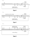
- FIG. 2 there is shown a partial cross-sectional view of a handling wafer structure 2 which includes a first substrate 101 and a plurality of defined insulator layers 102, 106, 108 and conductor layer(s) 104 formed over a first monocrystalline membrane wafer substrate 101.
- the first substrate 101 may be formed with a highly doped (e.g., n-type) monocrystalline membrane wafer substrate material, such as a bulk insulator substrate, a bulk metal substrate, a bulk silicon substrate, single crystalline silicon (doped or undoped), semiconductor-on-insulator (SOI) substrate, a multi-layered composite film wafer substrate or any semiconductor material including, for example, Si, SiC, SiGe, SiGeC, Ge, GaAs, InAs, InP as well as other Group III-IV compound semiconductors or any combination thereof.
- a highly doped (e.g., n-type) monocrystalline membrane wafer substrate material such as a bulk insulator substrate, a bulk metal substrate, a bulk silicon substrate, single crystalline silicon (doped or undoped), semiconductor-on-insulator (SOI) substrate, a multi-layered composite film wafer substrate or any semiconductor material including, for example, Si, SiC, SiGe, SiGeC, Ge, GaAs, InAs
- a first insulator layer 102 is formed (e.g., grown or deposited).
- the surface of the first substrate 101 is cleaned and a thin (e.g., 2 microns) layer of oxide is thermally grown to passivate the first substrate 101 and to serve an etch stop for future structural silicon etch processing (described hereinbelow).
- a field oxide layer, local oxidation of silicon (LOCOS), or oxide-nitride-oxide (ONO) layer may be formed.
- the insulator layer 102 may be implemented as silicon dioxide or some low-k dielectric material, but may include other materials such as phosphor-silicate glass (PSG) oxide, fluorinated silicon glass (FSG) oxide, silicon nitride, and/or other types of dielectric, including low-K dielectric materials with high thermal conductivity for cooling.
- PSG phosphor-silicate glass
- FSG fluorinated silicon glass
- Si nitride silicon nitride
- other types of dielectric including low-K dielectric materials with high thermal conductivity for cooling.
- a first conductive layer 104 may be formed, such as by depositing a poly layer 104 that may be doped or implanted to form the first conductive layer 104.
- an epitaxial growth process may be used to form the depicted interconnect substrate contacts 104A-E from exposed portions of the first substrate 101, followed by an optional patterned etch process and/or planarization or polishing step for form the interconnect substrate contacts 104A-E.
- the patterned first conductive layer 104 forms various mechanical and electrical functional structures such as vertical stop, vertical sensing electrodes, electrical interconnects, and bond ring structures on the first MEMS wafer device 100.
- the first conductive layer 104 is formed on the patterned insulator layer 102 and exposed first substrate 101 using any desired epitaxial growth, deposition, or sputtering process, such as chemical vapor deposition (CVD), plasma-enhanced chemical vapor deposition (PECVD), physical vapor deposition (PVD), atomic layer deposition (ALD), molecular beam deposition (MBD) or any combination(s) thereof.
- CVD chemical vapor deposition
- PECVD plasma-enhanced chemical vapor deposition
- PVD physical vapor deposition
- ALD atomic layer deposition
- MBD molecular beam deposition
- a suitable material for use as the first conductive layer 104 is doped polysilicon layer that is deposited to a predetermined thickness of less than 5 microns (e.g., 0.2-1 microns), though other conductive materials with different thicknesses may be used.
- the pattern transfer and etching of the first conductive layer 104 may use one or more etching steps to remove the unprotected portions of the first conductive layer 104, including a dry etching process such as reactive-ion etching, ion beam etching, plasma etching or laser etching, a wet etching process wherein a chemical etchant is employed or any combination thereof.
- a dry etching process such as reactive-ion etching, ion beam etching, plasma etching or laser etching, a wet etching process wherein a chemical etchant is employed or any combination thereof.
- a dry etching process such as reactive-ion etching, ion beam etching, plasma etching or laser etching
- a wet etching process wherein a chemical etchant is employed or any combination thereof.
- one or more additional insulators and/or conductive layers may also be formed over the first conductive layer 104 with additional de
- the first conductive layer 104 is formed by depositing a doped polysilicon layer
- the bottom surface of the first conductive layer 104 is relatively smooth when formed on an underlying thermal oxide or insulator layer 102 which has a relatively smooth upper surface.
- the upper or top surface of the first conductive layer 104 is relatively rough due to the nature of the polycrystalline structure resulting from the poly deposition process.
- a second insulator layer 106 may be formed, such as by depositing a layer of field nitride or alumina (Al 2 0 3 ) over the semiconductor wafer structure 2 to cover the patterned first conductive layer 104, followed by an optional selective pattern and etch process to selectively form defined insulator layers 106. Subsequently, a planarized dielectric or insulator layer 108 may be formed over the defined insulator layers 106 to cover the semiconductor wafer structure 2.
- the planarized dielectric layer 108 may be formed by depositing and planarizing a layer of tetra-ethyl ortho-silicate (TEOS) or silane-based oxide over the semiconductor wafer structure 3 to cover the second insulator layer 106 and first conductive layer 104 and the patterned openings therein.
- TEOS tetra-ethyl ortho-silicate
- a chemical mechanical polish process or other planarization step may be applied to planarize the planarized dielectric layer 108.
- the handle wafer structure 110 is a single crystal silicon wafer with good surface smoothness, and provides mechanical support for subsequent processing of the monocrystalline membrane wafer structure 101.
- a suitable cleaning step is performed prior to attaching the handle wafer structure 110 and membrane wafer structure 101 to prepare the handle wafer structure 110 for subsequent fusion bonding.
- the single crystal silicon layer 101 may be thinned to a suitable or targeted thickness to form the eventual MEMS device layer.
- a recess or polish process may be applied to thin the deposited membrane wafer substrate layer 101 down to a predetermined thickness (e.g., approximately 25 microns), though other thicknesses may be desired.
- a Germanium (Ge) layer may also be deposited and patterned on the top surface of the monocrystalline membrane wafer structure 101 to prepare for eutectic bonding with the cap wafer later.
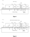
- FIG. 5 there is shown a partial cross-sectional view of the handling wafer structure 5 after applying a patterned etch process 111 to the membrane wafer substrate layer 101 to form openings 111A-E which expose the underlying first insulator layer 102 and which define patterned monocrystalline membrane wafer structural elements 101A-F.
- one or more selective etch processes are applied to form the interconnect, bond, and seal ring structures, as well as the MEMS transducer elements, such as any mechanical elements in the MEMS sensor (e.g., a gyroscope sensor).
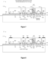
- FIG. 6 there is shown a partial cross-sectional view of the handling wafer structure 6 after applying one or more MEMS structural release etch process 112 to selectively remove exposed portions of the first insulator layer 102 and form electrode openings 112A-D, thereby defining all of the component parts of the MEMs sensor device.
- component parts include the structural connection elements (e.g., 101B) and the bond ring structures (e.g., 101A, 101F) which are fixedly coupled to the handle wafer substrate 110.
- the component parts also include the seal ring structures (e.g., 101C, 101E) which are fixedly coupled to the handle wafer substrate 110 to surround the polycrystalline MEMS proof mass 101D.
- the component parts include the mechanical elements 101D of the MEMS sensor device, such as one or more proof mass structures, plates, flexures, frame, and hinges (not shown).
- the release etch process 112 may include a vapor release etch (VPE) which is applied to remove the thermal oxide layer 102 from below the MEMS proof mass 101D, thereby releasing these elements.
- VPE vapor release etch
- vHF vapor hydrofluoric acid
- the release etch process 112 also removes part of the first insulator layer 102 as part of the opening which will expose the bond pad area 111A in the finally formed MEMS device wafer assembly.
- one or more processing steps 113 may include applying a non-homogeneous etch step which is controlled to non-uniformly etch the exposed surfaces 115E of the patterned poly electrode layer 104D.
- a non-homogeneous etch process 113 may employ a plasma etch using sulfur hexafluoride (SF 6 ) and oxygen (O 2 ) chemistry or a carbon fluorine chemistry which etches at least the poly grain boundaries and nearby areas faster on the upper sensing gap surface 115E of the poly electrode layer 104D, creating valleys in the grain boundary areas and peaks in the non-boundary regions. As a result, the surface roughness of the roughened or abraded patterned poly electrode layer 104D at the sensing gap surface 115E is increased.
- SF 6 sulfur hexafluoride
- O 2 oxygen
- the processing steps 113 may include a very thin and non-uniform polymer deposition step, followed by a silicon etch step which etches the surface layers where formed and, in the process, removes the non-uniform polymer layer.
- the polymer deposition step With the polymer deposition step, the sensing gap surfaces at the bottom of the patterned membrane wafer substrate layers 101A-F and at the top of the sensing poly gate electrode 104D are coated with the non-uniform polymer.
- all exposed surfaces of the layers 101A-F, 104D will be coated with the polymer layer, but the relevant area of interest is the sensing gap surfaces.
- the non-uniform polymer deposition step may use a carbon fluorine chemistry to deposit the very thin and non-uniform polymer layers 114A-F, 115E. Due to the nature of the non-uniform polymer layers 114, 115, the subsequent silicon etching step results in a non-uniform etching of the sensing gap surfaces since the removal of the non-uniform polymer layers 114, 115 shields the underlying surfaces (but not the exposed surfaces) from etching, resulting in peak and valleys in the sensing gap surfaces 114 at the bottom of the patterned membrane wafer substrate layers 101A-F and in the sensing gap surface 115 at the top of the sensing electrode 104D.
- a suitable etch process can be a fluorine or chlorine etch chemistry.
- the patterned bond anchor elements 116A-C, 116E-F are formed as patterned germanium anchor elements by depositing a layer of germanium 116 on the semiconductor wafer structure 8.
- the top surface of the semiconductor wafer structure 8 may be cleaned, and then a layer of germanium may be formed and then patterned and etched using the patterned resist or mask layer (not shown) to define germanium interconnect structures 116A-C, 116E-F in the interconnect, bond ring, and seal ring areas.
- the deposited germanium layer 116 may be covered by a patterned hardmask layer (e.g., TEOS) that is used to both etch the germanium layer 116 and protect the resulting patterned germanium bond anchor elements 116A-C, 116E-F during subsequent etching of the membrane wafer substrate layer 101.
- a patterned hardmask layer e.g., TEOS
- the cap wafer structure 200 includes a second substrate 201 and a plurality of defined insulator layers 202, 206, 208, 210, and conductor layers 204, 212 that are formed and patterned over the second substrate 201.
- the second substrate 201 may be implemented with monocrystalline semiconductor material, such as a bulk insulator substrate, a bulk metal substrate, a bulk silicon substrate, single crystalline silicon (doped or undoped), semiconductor-on-insulator (SOI) substrate, a multi-layered composite film wafer substrate or any semiconductor material including, for example, Si, SiC, SiGe, SiGeC, Ge, GaAs, InAs, InP as well as other Group III-IV compound semiconductors or any combination thereof.
- a protective insulator layer 201A may be formed, such as by thermally growing an oxide layer 201a (e.g., silicon oxide) to a predetermined thickness.
- a first insulator layer 202 is formed (e.g., grown or deposited) on a first or top surface of the second substrate 201, such as by cleaning the surface of the second substrate 201 and then thermally growing a thin (e.g., 2 microns) layer of passivation oxide or other insulator material, such as PSG oxide, FSG oxide, silicon nitride, and/or other types of dielectric, including low-K dielectric materials with high thermal conductivity for cooling.
- passivation oxide or other insulator material such as PSG oxide, FSG oxide, silicon nitride, and/or other types of dielectric, including low-K dielectric materials with high thermal conductivity for cooling.
- the first insulator layer 202 may be patterned and selectively etched to form one or more openings to expose the second substrate 201.
- a patterned masking layer (not shown) may be formed over the insulator layer 202, and a selective etch process may be applied to form openings in the insulator layer 202 that expose the second substrate 201 which provide an electrical interconnect path to conductive lines or paths (not shown) in the substrate 201.
- a first conductive layer 204 may be formed by depositing a metal or conductive polysilicon layer on the cap wafer structure 200 using any desired deposition or sputtering process, such as CVD, PECVD, PVD, ALD, MBD or any combination(s) thereof.
- the first conductive layer may be a deposited aluminum layer.
- the first conductive layer 204 may be patterned and etched to define electrode, interconnect, and bond ring structures on the first cap wafer structure 200.
- a patterned resist or mask layer may be formed to protect predetermined portions of the first conductive layer 204 and exposed portions of the first conductive layer 204 may be selectively etched and removed, thereby leaving portions of the first conductive layer 204, including interconnect conductors 204A and interconnect substrate contacts 204B to the substrate 201, though other patterned conductive layers (e.g., interconnect structures and sensor electrode structures) may also be formed.
- the pattern transfer and etching of the first conductive layer 204 may use one or more etching steps to remove the unprotected portions of the first conductive layer 204, including a dry etching process such as reactive-ion etching, ion beam etching, plasma etching or laser etching, a wet etching process wherein a chemical etchant is employed or any combination thereof.
- a dry etching process such as reactive-ion etching, ion beam etching, plasma etching or laser etching, a wet etching process wherein a chemical etchant is employed or any combination thereof.
- the patterned first conductive layer 204 is used for bonding the cap wafer structure 200 to the membrane wafer substrate structure 100.
- a patterned first conductive layer 204 of aluminum may be used for the dual purposes of conductive interconnect and Al-Ge bonding with the patterned bond anchor elements 116A-C, 116E-F, thereby eliminating the need to form separate standoff structures 206, 208, 210, 212 as described hereinbelow.
- separate standoff structures are formed on the patterned first conductive layer 204 by forming a second insulator layer 206 on the cap wafer structure 200, such as by depositing one or more interlayer dielectric (ILD) layers over the cap wafer structure 200 to a predetermined thickness.
- the second insulator layer 206 may be formed by depositing and planarizing a first cap oxide layer 206 over the cap wafer structure 200 to cover the first conductive layer 204 and the patterned openings therein.
- a cap etch stop layer 208 e.g., silicon nitride
- second cap oxide layer 210 are sequentially deposited, patterned, and etched to form patterned standoff elements 208/210 which are positioned for alignment with the patterned bond anchor elements 116A-C, 116E-F during bonding.
- one or more patterned etch processes may be applied to selectively etch the first cap oxide layer 206 and expose the underlying first conductive layer 204 at predetermined via openings.
- patterned cap metal bond anchor elements 212 are formed on the cap wafer structure 200.
- an aluminum layer may be deposited or sputtered to a predetermined thickness (e.g., 1-2 microns), though other deposition processes, materials, and thicknesses may be used.
- a photolithographic mask and etch processing is applied to define the aluminum bond anchor elements 212 which are positioned in the bond pad area and for alignment with the patterned bond anchor elements 116A-C, 116E-F from the first MEMS wafer device 100.
- Figure 9 shows two patterned interconnect layers 210, 212 are formed on the cap wafer structure 200, those skilled in the art will appreciate that the cap wafer structure 200 may also be formed with additional (three or more) or fewer (one) electrical interconnect layers.
- a cap cavity 207 may be formed in the second substrate 201 by patterning and etching the cap wafer structure 200.
- a patterned cap resist or mask layer (not shown) may be formed to expose and remove the cap oxide layer 206 over the intended cap cavity 207, followed by selectively removal of the exposed portions of the second substrate 201 to form a cap cavity 207 to a predetermined depth and width which is positioned for alignment with the patterned polycrystalline MEMS proof mass 101D from the MEMS wafer device 100.
- the pattern transfer and etching of the second substrate 201 may use one or more silicon etching steps, including a dry etching process such as reactive-ion etching, ion beam etching, plasma etching or laser etching, a wet etching process wherein a chemical etchant is employed or any combination thereof.
- a dry etching process such as reactive-ion etching, ion beam etching, plasma etching or laser etching, a wet etching process wherein a chemical etchant is employed or any combination thereof.
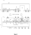
- the cap wafer structure 200 has been flipped upside down in preparation for bonding attachment 300 to the top of the fusion-bonded membrane/handle wafer structure 100.
- the handling wafer structure 100 and the cap wafer structure 200 may each be cleaned, such as by using a non-oxidizing ash chemistry or solvent-based wet removal process which does not oxidize the underlying metal layers.
- the MEMS handling wafer structure 100 and cap wafer structure 200 are bonded together using metal compression bonding techniques, such as a combination of thermal and pressure bonding.
- metal compression bonding techniques such as a combination of thermal and pressure bonding.
- AlGe bonding techniques may be used to provide both a hermetic sealing of the cavities (e.g., 207) enclosing the released MEMS structures, and the electrical connections between the MEMS structures to the cap wafer structure 200.
- the metal thermocompression bonding techniques described hereinabove provide a hermetic barrier between the MEMS transducer structures 101D (formed from the MEMS handling wafer structure 100) and the ambient environment which is superior to the sealing performance provided by oxide or glass sealing techniques.
- other bonding techniques may be used to obtain additional sealing protections.
- the bond anchor elements 116A-C, 116E-F are replaced with patterned germanium anchor elements 116A-C, 116E-F so that an aluminum-germanium eutectic bond may be formed to bond the MEMS handling wafer structure 100 and the cap wafer structure 200 together.
- the protective cap wafer structure 200 and MEMS handling wafer structure 100 are bonded together using an aluminum-germanium eutectic bond under vacuum conditions.
- the high aspect ratio polycrystalline MEMS proof mass structures 110D formed from the MEMS handling wafer structure 100 can be hermetically sealed.
- thermocompression bonding may be implemented by applying pressure at or above a predetermined threshold (e.g., 30MPa) in combination with a relatively low temperature heat process (e.g., at or below 500 degrees Celsius).
- thermocompression bonding may be implemented by aligning and compressing the first MEMS handling wafer structure 100 and cap wafer structure 200 with 70-90 kiloNewtons of force while heating the wafer structures 100, 200 to 400-500 degrees Celsius for approximately 30-50 minutes.
- the MEMS handling wafer structure 100 By attaching the MEMS handling wafer structure 100 to the first cap wafer structure 200 using a metal-to-metal bond technique, the MEMS transducer structures formed from the MEMS handling wafer structure 100 can be hermetically sealed by the bonding and seal ring structures 208/210/212/116/110/106/104.
- additional or different processing steps may be used to complete the fabrication of the depicted MEMS device wafer assembly into functioning devices.
- additional backend processing steps may be performed, such as forming contact plugs and multiple levels of interconnect(s) that are used to connect the device components in a desired manner to achieve the desired functionality.
- the specific sequence of steps used to complete the fabrication of the device components may vary, depending on the process and/or design requirements. It is understood that the terms so used are interchangeable under appropriate circumstances such that the embodiments of the invention described herein are, for example, capable of operation in other orientations than those illustrated or otherwise described herein.
- FIG. 10 depicts a simplified flow chart 10 showing the processing steps 1000-1009 for fabricating a MEMS sensor device with reduced Z-axis stiction.
- a membrane wafer having a poly electrode layer and monocrystalline proof mass layer is fabricated (step 10001).
- the membrane wafer 101 may be fabricated on a first crystal silicon wafer substrate using a sequence of processing steps to deposit, pattern and etch insulator layers and conductive poly sense electrode layers to define MEMS wafer interconnect layers and sense electrode layers.
- Figure 3 shows a semiconductor wafer structure 3 having a monocrystalline proof mass layer 101, a plurality of insulator layers 102, 106, 108, conductive poly electrode layers 104, and one or more covering insulator layers 106, 108.
- a handle wafer 110 is fabricated.
- the handle wafer may be fabricated with a second crystal silicon wafer substrate.
- the membrane wafer 101 is bonded to the handle wafer.
- the handle wafer provides mechanical support for subsequent processing of the membrane wafer.
- Figure 4 shows the handling wafer structure 4 wherein a handling wafer 110 is bonded to the planarized dielectric layer 108 on the membrane wafer 101.
- the monocrystalline proof mass layer 101 of the membrane wafer 101 may be thinned to a targeted thickness to form the eventual MEMS device layer.
- a cap wafer is fabricated.
- the cap wafer may be fabricated with a third crystal silicon wafer substrate which is separately processed with a sequence of processing steps to deposit, pattern and etch insulator layers and conductive layers.
- the cap wafer may be processed to form an array of through silicon vias (TSVs) using a deep reactive ion etch (DRIE) process 111 to selectively etch the third crystal silicon wafer substrate, followed by a polysilicon deposition process and chemical mechanical polish step to form the TSVs.
- TSVs through silicon vias
- DRIE deep reactive ion etch
- the monocrystalline proof mass layer on the membrane wafer is selectively etched.
- a patterned transducer resist or mask layer is formed on the monocrystalline proof mass layer to protect selected portions of the monocrystalline proof mass layer, and then the exposed portions of the monocrystalline proof mass layer may be selectively etched and removed with a deep reactive ion etch (DRIE) process.
- DRIE deep reactive ion etch
- a release etch process is applied to the membrane wafer to release the monocrystalline MEMS proof mass elements.
- the release etch process may include a vapor release etch (VPE) that is applied to remove a sacrificial dielectric or insulator layer from below the MEMS proof mass elements, thereby releasing these elements.
- VPE vapor release etch
- the membrane wafer and handle wafer are bonded to the cap wafer.
- the cap wafer is bonded with the combined membrane/handle wafer using AlGe eutectic bonding.
- cap wafer may be thinned, and contacts to the TSV and redistribution routing layers (RDLs) are fabricated before the final passivation step.
- RDLs redistribution routing layers
- step 1009 the fabrication process ends.
- the disclosed MEMS sensor device includes a first inertial transducer element formed in a multi-layer semiconductor structure.
- the first inertial transducer element is a z-axis accelerometer sensor.
- the disclosed MEMS sensor device also includes a cap device bonded to the multi-layer semiconductor structure to protect the first inertial transducer element from ambient environmental conditions.
- the cap device is bonded to the multi-layer semiconductor structure with a high temperature eutectic seal ring bonding structure to form a vacuum in a first sensor cavity which houses the first inertial transducer element.
- the first inertial transducer element includes a first monocrystalline semiconductor proof mass element and a second conductive electrode element separated from one another by an air sensing gap.
- the first monocrystalline semiconductor proof mass element is a cantilevered monocrystalline silicon beam anchored to the multi-layer semiconductor structure.
- the second conductive electrode element may include a conductive layer (e.g., conductive polycrystalline layer) formed in the multi-layer semiconductor structure to be positioned in alignment with but separated from the cantilevered monocrystalline silicon beam.
- At least a first sensing gap surface of the first monocrystalline semiconductor proof mass element is a first rough surface that has been selectively etched to reduce stiction between the first monocrystalline semiconductor proof mass element and the second conductive electrode element.
- at least a second sensing gap surface of the second conductive electrode element is a second rough surface that has been selectively etched to reduce stiction between the first monocrystalline semiconductor proof mass element and the second conductive electrode element.
- at least the first sensing gap surface of the first monocrystalline semiconductor proof mass element includes a non-uniform layer of deposited polymer that has been selectively etched to form the first rough surface on at least the first sensing gap surface.
- at least the second sensing gap surface of the second conductive electrode element includes a non-uniform layer of deposited polymer that has been selectively etched to form the second rough surface on at least the second sensing gap surface.
- a transducer and associated method for fabrication in another form, there is provided a transducer and associated method for fabrication.
- a MEMS wafer structure in the disclosed methodology, includes a first semiconductor electrode and a first semiconductor layer that is formed over the first semiconductor electrode.
- the first semiconductor electrode is formed as a polycrystalline silicon electrode, and the first semiconductor layer is formed as a first monocrystalline semiconductor layer.
- the first semiconductor electrode is formed as a polycrystalline silicon electrode, and the first semiconductor layer is formed as a first polycrystalline semiconductor layer.
- the disclosed method also includes selectively etching the first semiconductor layer to form a first MEMS inertial transducer element and surrounding frame support elements.
- the first semiconductor layer is selectively etched by etching the first semiconductor layer with a deep reactive ion etch process to form the first MEMS inertial transducer element as a high aspect ratio proof mass transducer element (e.g., a z-axis accelerometer sensor).
- the disclosed method includes applying a structural release etch process to release the first MEMS inertial transducer element and to expose a first sensing gap surface of the first MEMS inertial transducer element and a second sensing gap surface of the first semiconductor electrode.
- the structural release etch process may be applied using a vapor release etch to remove a sacrificial dielectric layer formed between the semiconductor electrode and the first semiconductor layer.
- the disclosed method also includes applying a surface abrasion etch process to roughen one or both of the first sensing gap surface of the first MEMS inertial transducer element or the second sensing gap surface of the first semiconductor electrode, thereby reducing stiction between the first MEMS inertial transducer element and the first semiconductor electrode.
- the surface abrasion etch process may be applied using a non-homogeneous plasma etch which etches crystalline grain boundary regions in either or both of the first MEMS inertial transducer element or the first semiconductor electrode faster than non-boundary regions in either or both of the first MEMS inertial transducer element or the first semiconductor electrode.
- the surface abrasion etch process may be applied by depositing a non-uniform polymer layer on at least the first and second sensing gap surfaces; and applying a semiconductor etch process which roughens the first and second sensing gap surfaces by selectively etching the first MEMS inertial transducer element and the first semiconductor electrode not protected by the non-uniform polymer layer.
- the disclosed method includes attaching a first cap wafer structure to the MEMS wafer structure using a first bonding process.
- the first cap wafer structure may be attached to the MEMS wafer structure by bonding the first cap wafer structure to the MEMS wafer structure with a high temperature eutectic seal ring bonding structure to form a vacuum in a first sensor cavity of the cap wafer structure which houses the first MEMS inertial transducer element.
- a high aspect ratio transducer and method for making same includes a first cap structure which includes a substrate, a plurality of first metal interconnect bond spacer structures, and a high vacuum cavity formed in the substrate to define a first inertial transducer space.
- the disclosed transducer also includes a first semiconductor substrate structure attached to the plurality of first metal interconnect bond spacer structures, where the first semiconductor substrate structure includes a first surface on which a second patterned metallic layer is formed and bonded to the plurality of first metal interconnect bond spacer structures, a first high aspect ratio proof mass element which is aligned with the first inertial transducer space, and a second surface on which a plurality of spacer structures are formed to define an out-of-plane semiconductor sensing electrode space.
- the disclosed transducer includes a second semiconductor substrate structure attached to the plurality of spacer structures and comprising an out-of-plane semiconductor sensing electrode which is aligned with the first high aspect ratio proof mass element.
- At least a first sensing gap surface of the first high aspect ratio proof mass element is a first rough surface that has been selectively etched to reduce stiction between the first high aspect ratio proof mass element and the out-of-plane semiconductor sensing electrode.
- the first high aspect ratio proof mass element is a cantilevered monocrystalline silicon beam anchored to the first semiconductor substrate structure
- the out-of-plane semiconductor sensing electrode is a polycrystalline silicon electrode layer formed in the second semiconductor substrate structure.
- at least second sensing gap surface of the out-of-plane semiconductor sensing electrode is a second rough surface that has been selectively etched to reduce stiction between the first high aspect ratio proof mass element and the out-of-plane semiconductor sensing electrode.
- the methodology of the present disclosure may be applied using materials other than expressly set forth herein.
- the process steps may be performed in an alternative order than what is presented. For example, the sequence of wafer bonding steps may be reversed.
- certain layers of materials will be deposited and removed to form the depicted MEMS device wafer structures. Where the specific procedures for depositing or removing such layers are not detailed, any desired technique may be used for depositing, removing or otherwise forming such layers at appropriate thicknesses. Such details are well known and not considered necessary to teach one skilled in the art of how to make or use the present disclosure.
- MEMS devices may be implemented with accelerometer and/or gyroscope sensors
- the fabrication process described herein is not limited to such MEMS sensors or any other type of sensor, but is also applicable to any one of numerous MEMS devices that include some type of structure that is movably suspended by one or more springs and that is formed by bonding an active wafer to a reference wafer.
- Non-limiting examples of such devices include various types of accelerometers and switches, optical MEMS system components, and other MEMS system devices that use drive and sense electrodes.
Landscapes
- Engineering & Computer Science (AREA)
- Microelectronics & Electronic Packaging (AREA)
- Computer Hardware Design (AREA)
- Manufacturing & Machinery (AREA)
- Physics & Mathematics (AREA)
- General Physics & Mathematics (AREA)
- Mechanical Engineering (AREA)
- Health & Medical Sciences (AREA)
- General Health & Medical Sciences (AREA)
- Toxicology (AREA)
- Pressure Sensors (AREA)
Abstract
Description
- The present disclosure is directed in general to the field of semiconductor devices. In one aspect, the present disclosure relates to MEMS devices and methods for fabricating MEMS devices.
- Micro-Electro-Mechanical Systems (MEMS) technology is increasingly used to integrate mechanical elements, sensors, actuators, and electronics on a common silicon substrate through microfabrication technology. For example, inertial sensors may be formed with MEMS devices on an integrated circuit wafer substrate to form various applications, such accelerometers for measuring linear acceleration, gyroscopes for measuring angular velocity, optical devices, pressure sensors, switches, and so forth. A conventional MEMS device typically includes a moveable element, such as a proof mass, diaphragm, mirror, and the like that is flexible or movable, and is attached to the rest of the device. Relative motion between this movable element and the rest of the device is driven by actuators and/or sensed by sensors in various ways, depending on device design. With existing semiconductor processing techniques, it has been observed that Z-axis accelerometer devices are more prone to stiction. One of the reasons for this is that there is a higher likelihood of stiction between the very smooth contact surface of the single crystal silicon proof mass and the very smooth contact surface of the polysilicon electrode surface. While anti-stiction coatings have been proposed for use with forming accelerometer sensors, such coatings can interfere with the eutectic bonding process used to form gyrometer sensors. As a result, the existing design, operation, and manufacturability of integrated circuit MEMS sensors are extremely difficult to implement at a practical level.
- In accordance with a first aspect of the present disclosure, a MEMS sensor device is provided, comprising: a first inertial transducer element formed in a multi-layer semiconductor structure; and a cap device bonded to the multi-layer semiconductor structure to protect the first inertial transducer element from ambient environmental conditions, where the first inertial transducer element comprises a first monocrystalline semiconductor proof mass element and a second conductive electrode element separated from one another by an air sensing gap, and where at least a first sensing gap surface of the first monocrystalline semiconductor proof mass element is a first rough surface that has been selectively etched to reduce stiction between the first monocrystalline semiconductor proof mass element and the second conductive electrode element.
- In one or more embodiments, at least a second sensing gap surface of the second conductive electrode element is a second rough surface that has been selectively etched to reduce stiction between the first monocrystalline semiconductor proof mass element and the second conductive electrode element.
- In one or more embodiments, the first inertial transducer element comprises a z-axis accelerometer sensor.
- In one or more embodiments, the first monocrystalline semiconductor proof mass element comprises a cantilevered monocrystalline silicon beam anchored to the multi-layer semiconductor structure.
- In one or more embodiments, the second conductive electrode element comprises a conductive polysilicon layer formed in the multi-layer semiconductor structure to be positioned in alignment with but separated from the cantilevered monocrystalline silicon beam.
- In one or more embodiments, the cap device is bonded to the multi-layer semiconductor structure with a high temperature eutectic seal ring bonding structure to form a vacuum in a first sensor cavity which houses the first inertial transducer element.
- In one or more embodiments, at least the first sensing gap surface of the first monocrystalline semiconductor proof mass element includes a non-uniform layer of deposited polymer that has been selectively etched to form the first rough surface.
- In one or more embodiments, at least the second sensing gap surface of the second conductive electrode element includes a non-uniform layer of deposited polymer that has been selectively etched to form the second rough surface.
- In accordance with a second aspect of the present disclosure, a method for fabricating a transducer is conceived, comprising: providing a MEMS wafer structure comprising a first semiconductor electrode and a first semiconductor layer that is formed over the first semiconductor electrode; selectively etching the first semiconductor layer to form a first MEMS inertial transducer element and surrounding frame support elements; applying a structural release etch process to release the first MEMS inertial transducer element and to expose a first sensing gap surface of the first MEMS inertial transducer element and a second sensing gap surface of the first semiconductor electrode; applying a surface abrasion etch process to roughen one or both of the first sensing gap surface of the first MEMS inertial transducer element or the second sensing gap surface of the first semiconductor electrode, thereby reducing stiction between the first MEMS inertial transducer element and the first semiconductor electrode; and attaching a first cap wafer structure to the MEMS wafer structure using a first bonding process.
- In one or more embodiments, providing the MEMS wafer structure comprises forming the first semiconductor electrode as a polycrystalline silicon electrode over which the first semiconductor layer is formed as a first monocrystalline semiconductor layer.
- In one or more embodiments, providing the MEMS wafer structure comprises forming the first semiconductor electrode as a polycrystalline silicon electrode over which the first semiconductor layer is formed as a first polycrystalline semiconductor layer.
- In one or more embodiments, selectively etching the first semiconductor layer comprises etching the first semiconductor layer with a deep reactive ion etch process to form the first MEMS inertial transducer element as a high aspect ratio proof mass transducer element.
- In one or more embodiments, the high aspect ratio proof mass transducer element comprises a z-axis accelerometer sensor.
- In one or more embodiments, applying the structural release etch process comprises applying a vapor release etch to remove a sacrificial dielectric layer formed between the semiconductor electrode and the first semiconductor layer.
- In one or more embodiments, applying the surface abrasion etch process comprises applying a non-homogeneous plasma etch which etches crystalline grain boundary regions in either or both of the first MEMS inertial transducer element or the first semiconductor electrode faster than non-boundary regions in either or both of the first MEMS inertial transducer element or the first semiconductor electrode.
- In one or more embodiments, applying the surface abrasion etch process comprises: depositing a non-uniform polymer layer on at least the first and second sensing gap surfaces; and applying a semiconductor etch process which roughens the first and second sensing gap surfaces by selectively etching the first MEMS inertial transducer element and the first semiconductor electrode not protected by the non-uniform polymer layer.
- In one or more embodiments, attaching the first cap wafer structure to the MEMS wafer structure comprises bonding the first cap wafer structure to the MEMS wafer structure with a high temperature eutectic seal ring bonding structure to form a vacuum in a first sensor cavity of the cap wafer structure which houses the first MEMS inertial transducer element.
- In accordance with a third aspect of the present disclosure, a high aspect ratio transducer is provided, comprising: a first cap structure comprising a substrate, a plurality of first metal interconnect bond spacer structures, and a high vacuum cavity formed in the substrate to define a first inertial transducer space; a first semiconductor substrate structure attached to the plurality of first metal interconnect bond spacer structures, the first semiconductor substrate structure comprising: a first surface on which a second patterned metallic layer is formed and bonded to the plurality of first metal interconnect bond spacer structures, a first high aspect ratio proof mass element which is aligned with the first inertial transducer space, and a second surface on which a plurality of spacer structures are formed to define an out-of-plane semiconductor sensing electrode space; and a second semiconductor substrate structure attached to the plurality of spacer structures and comprising an out-of-plane semiconductor sensing electrode which is aligned with the first high aspect ratio proof mass element, where at least a first sensing gap surface of the first high aspect ratio proof mass element is a first rough surface that has been selectively etched to reduce stiction between the first high aspect ratio proof mass element and the out-of-plane semiconductor sensing electrode.
- In one or more embodiments, the first high aspect ratio proof mass element comprises a cantilevered monocrystalline silicon beam anchored to the first semiconductor substrate structure, where the out-of-plane semiconductor sensing electrode comprises a polycrystalline silicon electrode layer formed in the second semiconductor substrate structure.
- In one or more embodiments, at least second sensing gap surface of the out-of-plane semiconductor sensing electrode is a second rough surface that has been selectively etched to reduce stiction between the first high aspect ratio proof mass element and the out-of-plane semiconductor sensing electrode.
- The present disclosure may be understood, and its numerous objects, features and advantages obtained, when the following detailed description of a preferred embodiment is considered in conjunction with the following drawings.
-
Figure 1 is a simplified cross section view of a MEMS sensor device which includes MEMS transducer elements with reduced Z-axis stiction in accordance with selected embodiments of the present disclosure. -
Figures 2-9 are simplified cross section views of various exemplary fabrication steps for making the MEMS sensor device shown inFigure 1 in accordance with selected embodiments of the present disclosure. -
Figure 10 depicts a simplified flow chart showing the processing steps for fabricating a MEMS sensor device with reduced Z-axis stiction in accordance with selected embodiments of the present disclosure. - A method and apparatus are described for fabricating high aspect ratio transducers (i.e., an "inertial transducer element") in a MEMS device wafer assembly by applying one or more non-homogeneous etch and/or deposition process step(s) to roughen at least one of the contact surfaces of the single crystal silicon proof mass and/or the polysilicon electrode, thereby reducing Z-axis stiction for the MEMS device. By creating at least one rough surface, the effective contact area when the proof-mass touches the bottom electrode is significantly reduced, thereby reducing the adhesion force and contact stiction. In selected embodiments, a MEMS device wafer having a deposited polycrystalline electrode layer and a monocrystalline substrate or proof mass layer is subjected to a first patterned transducer etch process of the monocrystalline substrate or proof mass layer to form one or more monocrystalline proof mass elements, including a movable sensor proof mass used for a MEMS sensor (e.g., a gyroscope sensor mass), and is then subjected to a non-homogeneous etch step that non-uniformly etches the surface of the monocrystalline proof mass element(s) and the polysilicon electrode layer. By choosing a non-homogeneous etch process which etches the grain boundaries and nearby areas of the polysilicon electrode layer faster than the rest of the polysilicon electrode layer, valleys are created in the grain boundary areas and peaks are created in the non-boundary regions. As a result, the surface roughness of polysilicon electrode layer is increased. In other selected embodiments, a MEMS device wafer with one or more patterned monocrystalline proof mass elements is subjected to a very thin and non-uniform polymer deposition step and a subsequent silicon etch step. By depositing a suitable non-uniform polymer, the subsequent silicon etching step will non-uniformly etch the patterned monocrystalline proof mass elements, resulting in peaks and valleys in the patterned monocrystalline proof mass element(s). This method can increase the surface roughness in both the single crystal silicon surface of the patterned monocrystalline proof mass element(s) and the polysilicon electrode layer. As will be appreciated, additional processing may be used to form one or more sensor electrodes, driver electrodes, and/or interconnect routing in the MEMS device.
- Referring now to
Figure 1 , there is shown a simplified cross section view of a MEMS sensordevice wafer assembly 1 that includes a cap wafer structure (i.e., a "cap device") 200 attached or affixed to aMEMS wafer device 100 which includes one or more of MEMS transducer sensor elements (i.e., "MEMS inertial elements") that are formed in a multi-layer semiconductor structure with reduced Z-axis stiction in accordance with selected embodiments of the present disclosure. Generally speaking, theMEMS wafer device 100 is formed on a monocrystalline semiconductor membrane wafer substrate 101 (i.e., "first substrate") by selectively forminganchor elements 102/104A-E/106, which include depositedpolysilicon layers 104D (i.e., a polysense electrode layer 104D) on the monocrystallinemembrane wafer substrate 101, along with a planarizeddielectric layer 108 and patterned bond anchor elements 116. At exposedsensing gap surfaces 114A-F (i.e., "first sensing gap surface") at the monocrystallineproof mass elements 101D (i.e., "first monocrystalline semiconductor proof mass elements") and a polysense electrode layer 104D/115E (i.e., "second conductive electrode element"), abraded or rough surface layers are formed (referred to collectively as abraded or roughed surface layers 114). In addition, the cap wafer structure 200 (i.e., "cap device") is formed on amonocrystalline semiconductor wafer 201 by selectively formingdefined insulator layers monocrystalline semiconductor wafer 201 to form anetched cap cavity 207, and then selectively forming metalbond anchor elements 208/210/212. - In the depicted
MEMS wafer device 100, the MEMS transducer sensor element may be a gyro sensor formed with a high aspect ratio monocrystalline semiconductor proofmass element monocrystalline 101D withabraded surfaces 114D (i.e., "first rough surfaces") and one or more out-of-planepolycrystalline sensing electrodes 104D/115E that are integrated with theMEMS wafer device 100 that is attached or bonded to acap wafer structure 200 using metal compression bonding techniques. As used herein, and in some embodiments, an "abraded" or "roughed surface" means a surface having a roughness average (RA) of between about 150 angstroms and about 500 angstroms. In other embodiments, a roughed or abraded surface may have an RA between about 100 and about 1,000 angstroms, although other higher or lower RA values may be used. In addition or in the alternative, an "abraded" or "roughed surface" may refer to a polycrystalline semiconductor layer having peaks and/or valleys formed on the surface of the polycrystalline semiconductor layer, such as etched or recessed valleys at the poly grain boundaries and nearby areas and/or peaks at the non-boundary surface areas. In addition or in the alternative, an "abraded" or "roughed surface" may refer to a monocrystalline semiconductor layer having peaks and valleys on the surface of the monocrystalline semiconductor layer that are formed by depositing a non-uniform polymer layer on the surface of the monocrystalline semiconductor layer, followed by an etch process which removes the non-uniform polymer layer to form the peaks and valleys on the surface of the monocrystalline semiconductor layer. As will be appreciated, the MEMS transducer sensor element can represent any type of MEMS sensor (such as an accelerometer, a gyroscope, etc.), and any number of MEMS sensor devices could be formed in either or both of theMEMS wafer device 100 andcap wafer structure 200. - As formed, the MEMS transducer sensor element may include a monocrystalline semiconductor
proof mass element 101D that is formed under ahigh vacuum cavity 207 in thecap wafer structure 200 and suspended within the monocrystalline semiconductormembrane wafer substrate 101 by, for example, one or more suspension springs (not shown). In other embodiments, the monocrystalline semiconductorproof mass element 101D may be formed as a cantilevered monocrystalline silicon beam anchored to a multi-layer semiconductor structure. As disclosed herein and indicated with the cross-hatching, roughened orabraded surfaces 114A-F are formed on at least the monocrystallineMEMS proof mass 101D (if not also the one or morestructural connection elements 101A-C, 101E-F) by applying one or more non-homogeneous etch and/or deposition process step(s). The MEMS transducer sensor element may also include one or morepolycrystalline sensing electrodes 104D/115E which are positioned to detect vibrational movement of the monocrystallineMEMS proof mass 101D/114D. In addition, the MEMS transducer sensor element includes one or morestructural connection elements 101A-C, 101E-F formed in the monocrystalline semiconductormembrane wafer layer 101 which are fixedly coupled to the cap wafer structure 200 (by the metalbond anchor elements 208/210/212/116) and to the monocrystalline handle wafer substrate layer 110 (by thebond anchor elements 102/104/106/108). In addition to serving as a mechanical anchor of theproof mass 101D/114D to the surrounding frame, the structural connection elements (e.g., 101C, 101E) may also function as a seal ring structure to provide a vacuum seal for thehigh vacuum cavity 207 when the firstMEMS wafer device 100 and firstcap wafer structure 200 are bonded together, such as by using a eutectic bonding process. In addition or in the alternative, the structural connection elements (e.g., 101A, 101F) may also function as bond ring structures which are formed to fixedly couple the firstMEMS wafer device 100 to the firstcap wafer structure 200 across metalbond anchor elements 208/210/212/116) and to the monocrystalline handle wafer substrate layer 110 (by thebond anchor elements 106/104/102). In addition or in the alternative, the structural connection elements (e.g., 101B, 101E) may also function as electrical interconnect structures which provide an electrical connection between one part of the circuit in the firstMEMS wafer device 100 and another circuit in the firstcap wafer structure 200. - Though shown in simplified cross section view, it will be appreciated that the MEMS sensor
device wafer assembly 1 may also include one or more non-illustrated moving electrodes and one or more non-illustrated fixed electrodes. The moving electrodes may form part of the suspendedsensor structures 101D/114D, and the fixed electrodes may be fixedly coupled to the monocrystallinemembrane wafer layer 101 and/or monocrystallinehandle wafer layer 110. The specific structure and configuration of the MEMS sensor may vary. Moreover, a description of the specific structure and configuration of the MEMS sensor is not needed to enable or fully describe the present disclosure, and will thus not be further described in more detail. - Having described an embodiment of a MEMS sensor
device wafer assembly 1 from a structural standpoint, an example process sequence for fabricating the MEMS sensordevice wafer assembly 1 will now be described with reference toFigures 2-9 which depict simplified cross section views of various exemplary fabrication steps for making the MEMS sensor device in accordance with selected embodiments of the present disclosure. While the depicted process sequence is provided with reference to making the MEMS sensordevice wafer assembly 1 shown inFigure 1 , it will be appreciated that the process is applicable to any one of numerous other MEMS devices, and that there are additional process steps that are not described, as these may be formed using any one of numerous processes, now known or developed in the future. Moreover, although for convenience the method is described using a particular order of steps, portions of the method could be performed in a different order or using different types of steps than what is described below. - Referring first to
Figure 2 , there is shown a partial cross-sectional view of a handlingwafer structure 2 which includes afirst substrate 101 and a plurality of defined insulator layers 102, 106, 108 and conductor layer(s) 104 formed over a first monocrystallinemembrane wafer substrate 101. Depending on the type of device being fabricated, thefirst substrate 101 may be formed with a highly doped (e.g., n-type) monocrystalline membrane wafer substrate material, such as a bulk insulator substrate, a bulk metal substrate, a bulk silicon substrate, single crystalline silicon (doped or undoped), semiconductor-on-insulator (SOI) substrate, a multi-layered composite film wafer substrate or any semiconductor material including, for example, Si, SiC, SiGe, SiGeC, Ge, GaAs, InAs, InP as well as other Group III-IV compound semiconductors or any combination thereof. Though not shown, one or more alignment mark(s) can be formed in thefirst substrate 101 to assist with pattern etching using any desired marking process. - On a first or top surface of the
first substrate 101, afirst insulator layer 102 is formed (e.g., grown or deposited). In selected embodiments, the surface of thefirst substrate 101 is cleaned and a thin (e.g., 2 microns) layer of oxide is thermally grown to passivate thefirst substrate 101 and to serve an etch stop for future structural silicon etch processing (described hereinbelow). In addition or in the alternative, a field oxide layer, local oxidation of silicon (LOCOS), or oxide-nitride-oxide (ONO) layer may be formed. Thus, theinsulator layer 102 may be implemented as silicon dioxide or some low-k dielectric material, but may include other materials such as phosphor-silicate glass (PSG) oxide, fluorinated silicon glass (FSG) oxide, silicon nitride, and/or other types of dielectric, including low-K dielectric materials with high thermal conductivity for cooling. - If desired, the
first insulator layer 102 may be patterned and etched to form one or more openings to expose thefirst substrate 101. Alternatively, a partial etch may be applied to form patterned recessed openings in thefirst insulator layer 102. Though not shown, a patterned masking layer may be formed over theinsulator layer 102, and any desired etching technique may be used to form the (recess) opening(s) in theinsulator layer 102. The defined openings in theinsulator layer 102 may provide an electrical interconnect path to thesubstrate 101 or otherwise define grounding contact regions to thefirst substrate 101 for a subsequently formed bond ring structure. - After forming the
patterned insulator layer 102, a first conductive layer 104 may be formed, such as by depositing a poly layer 104 that may be doped or implanted to form the first conductive layer 104. In other embodiments, an epitaxial growth process may be used to form the depictedinterconnect substrate contacts 104A-E from exposed portions of thefirst substrate 101, followed by an optional patterned etch process and/or planarization or polishing step for form theinterconnect substrate contacts 104A-E. When formed with a doped polysilicon layer, the patterned first conductive layer 104 forms various mechanical and electrical functional structures such as vertical stop, vertical sensing electrodes, electrical interconnects, and bond ring structures on the firstMEMS wafer device 100. In selected embodiments, the first conductive layer 104 is formed on the patternedinsulator layer 102 and exposedfirst substrate 101 using any desired epitaxial growth, deposition, or sputtering process, such as chemical vapor deposition (CVD), plasma-enhanced chemical vapor deposition (PECVD), physical vapor deposition (PVD), atomic layer deposition (ALD), molecular beam deposition (MBD) or any combination(s) thereof. A suitable material for use as the first conductive layer 104 is doped polysilicon layer that is deposited to a predetermined thickness of less than 5 microns (e.g., 0.2-1 microns), though other conductive materials with different thicknesses may be used. However the first conductive layer 104 is formed, a patterned resist or mask layer (not shown) may be formed on the first conductive layer 104 to protect predetermined portions of the first conductive layer 104, and the exposed portions of the first conductive layer 104 are selectively etched and removed, thereby leaving portions of the first conductive layer 104, includinginterconnect conductors 104A,interconnect substrate contacts substrate 101,structural connection elements 104C, andsensor electrode structures 104D in the movable mass or proof mass area. The pattern transfer and etching of the first conductive layer 104 may use one or more etching steps to remove the unprotected portions of the first conductive layer 104, including a dry etching process such as reactive-ion etching, ion beam etching, plasma etching or laser etching, a wet etching process wherein a chemical etchant is employed or any combination thereof. Though not shown, it will be appreciated that one or more additional insulators and/or conductive layers may also be formed over the first conductive layer 104 with additional deposition, pattern and etch processing steps. - In embodiments where the first conductive layer 104 is formed by depositing a doped polysilicon layer, it will be appreciated that the bottom surface of the first conductive layer 104 is relatively smooth when formed on an underlying thermal oxide or
insulator layer 102 which has a relatively smooth upper surface. However, it will also be appreciated that the upper or top surface of the first conductive layer 104 is relatively rough due to the nature of the polycrystalline structure resulting from the poly deposition process. - After forming the patterned first conductive layer 104, a
second insulator layer 106 may be formed, such as by depositing a layer of field nitride or alumina (Al203) over thesemiconductor wafer structure 2 to cover the patterned first conductive layer 104, followed by an optional selective pattern and etch process to selectively form defined insulator layers 106. Subsequently, a planarized dielectric orinsulator layer 108 may be formed over the defined insulator layers 106 to cover thesemiconductor wafer structure 2. - Referring now to
Figure 3 , there is shown a partial cross-sectional view of the handlingwafer structure 3 after a planarizeddielectric layer 108 is formed. In selected embodiments, the planarizeddielectric layer 108 may be formed by depositing and planarizing a layer of tetra-ethyl ortho-silicate (TEOS) or silane-based oxide over thesemiconductor wafer structure 3 to cover thesecond insulator layer 106 and first conductive layer 104 and the patterned openings therein. In addition, a chemical mechanical polish process or other planarization step may be applied to planarize the planarizeddielectric layer 108. - Referring now to
Figure 4 , there is shown a partial cross-sectional view of the handlingwafer structure 4 after the monocrystallinemembrane wafer structure 101 is flipped, attached to ahandle wafer structure 110, and thinned. In selected embodiments, thehandle wafer structure 110 is a single crystal silicon wafer with good surface smoothness, and provides mechanical support for subsequent processing of the monocrystallinemembrane wafer structure 101. Prior to attaching thehandle wafer structure 110 andmembrane wafer structure 101, a suitable cleaning step is performed to prepare thehandle wafer structure 110 for subsequent fusion bonding. After fusing the monocrystallinemembrane wafer structure 101 and handlewafer structure 110, the singlecrystal silicon layer 101 may be thinned to a suitable or targeted thickness to form the eventual MEMS device layer. For example, a recess or polish process may be applied to thin the deposited membranewafer substrate layer 101 down to a predetermined thickness (e.g., approximately 25 microns), though other thicknesses may be desired. Though not shown, a Germanium (Ge) layer may also be deposited and patterned on the top surface of the monocrystallinemembrane wafer structure 101 to prepare for eutectic bonding with the cap wafer later. - Referring now to
Figure 5 , there is shown a partial cross-sectional view of the handlingwafer structure 5 after applying apatterned etch process 111 to the membranewafer substrate layer 101 to formopenings 111A-E which expose the underlyingfirst insulator layer 102 and which define patterned monocrystalline membrane waferstructural elements 101A-F. In selected embodiments, one or more selective etch processes are applied to form the interconnect, bond, and seal ring structures, as well as the MEMS transducer elements, such as any mechanical elements in the MEMS sensor (e.g., a gyroscope sensor). For example, any suitable photolithography and deep reactive ion etch (DRIE) processes may be applied to fabricate the MEMS device structures using the single crystal silicon layer from themembrane wafer substrate 101. The selective etch of the membranewafer substrate layer 101 forms anopening 111A which will expose the bond pad area in the finally formed MEMS device wafer assembly, and also formsopenings 111B-E which define the patterned monocrystalline membrane waferstructural elements 101B-F. While the membranewafer substrate layer 101 may be structurally etched using a DRIE process to define theactive layer elements 101A-F, it will be appreciated that any desired pattern and etching processes may be used, including application and patterning of photoresist directly on the membrane waferstructural layer 101. In selected embodiments, the structural etch process is selected that is suitable for creating high-aspect ratio features. - Referring now to
Figure 6 , there is shown a partial cross-sectional view of the handlingwafer structure 6 after applying one or more MEMS structuralrelease etch process 112 to selectively remove exposed portions of thefirst insulator layer 102 andform electrode openings 112A-D, thereby defining all of the component parts of the MEMs sensor device. These component parts include the structural connection elements (e.g., 101B) and the bond ring structures (e.g., 101A, 101F) which are fixedly coupled to thehandle wafer substrate 110. The component parts also include the seal ring structures (e.g., 101C, 101E) which are fixedly coupled to thehandle wafer substrate 110 to surround the polycrystalline MEMSproof mass 101D. Finally, the component parts include themechanical elements 101D of the MEMS sensor device, such as one or more proof mass structures, plates, flexures, frame, and hinges (not shown). In selected embodiments, therelease etch process 112 may include a vapor release etch (VPE) which is applied to remove thethermal oxide layer 102 from below the MEMSproof mass 101D, thereby releasing these elements. For example, a single vapor hydrofluoric acid (vHF) etching step may be used to release the MEMSmechanical elements 101D by etching away exposed portions of thefirst insulator layer 102. Therelease etch process 112 also removes part of thefirst insulator layer 102 as part of the opening which will expose thebond pad area 111A in the finally formed MEMS device wafer assembly. - Referring now to
Figure 7 , there is shown a partial cross-sectional view of the handlingwafer structure 7 after applying one or more processing steps 113 to roughen or abrade sensing gap surfaces of the patterned membrane wafer substrate layers 101A-F and/orpoly electrode layer 104D, thereby forming roughened or abraded surface layers 114A-F, 115E. In selected embodiments, one or more processing steps 113 may include applying a non-homogeneous etch step which is controlled to non-uniformly etch the exposed surfaces 115E of the patternedpoly electrode layer 104D. For example, a non-homogeneous etch process 113 may employ a plasma etch using sulfur hexafluoride (SF6) and oxygen (O2) chemistry or a carbon fluorine chemistry which etches at least the poly grain boundaries and nearby areas faster on the uppersensing gap surface 115E of thepoly electrode layer 104D, creating valleys in the grain boundary areas and peaks in the non-boundary regions. As a result, the surface roughness of the roughened or abraded patternedpoly electrode layer 104D at thesensing gap surface 115E is increased. - In other selected embodiments, the processing steps 113 may include a very thin and non-uniform polymer deposition step, followed by a silicon etch step which etches the surface layers where formed and, in the process, removes the non-uniform polymer layer. With the polymer deposition step, the sensing gap surfaces at the bottom of the patterned membrane wafer substrate layers 101A-F and at the top of the sensing
poly gate electrode 104D are coated with the non-uniform polymer. Of course, all exposed surfaces of thelayers 101A-F, 104D will be coated with the polymer layer, but the relevant area of interest is the sensing gap surfaces. In an example embodiment, the non-uniform polymer deposition step may use a carbon fluorine chemistry to deposit the very thin andnon-uniform polymer layers 114A-F, 115E. Due to the nature of the non-uniform polymer layers 114, 115, the subsequent silicon etching step results in a non-uniform etching of the sensing gap surfaces since the removal of the non-uniform polymer layers 114, 115 shields the underlying surfaces (but not the exposed surfaces) from etching, resulting in peak and valleys in the sensing gap surfaces 114 at the bottom of the patterned membrane wafer substrate layers 101A-F and in the sensing gap surface 115 at the top of thesensing electrode 104D. In selected embodiments, a suitable etch process can be a fluorine or chlorine etch chemistry. As a result, the surface roughness of the roughened or abraded patterned poly layers 114A-F and sensingelectrode surface 104D/115E at the sensing gap surfaces is increased. - Referring now to
Figure 8 , there is shown a partial cross-sectional view of the handling wafer structure 8 after forming patternedbond anchor elements 116A-C, 116E-F on the top surface of the semiconductor wafer structure 8. In selected embodiments, the patternedbond anchor elements 116A-C, 116E-F are formed as patterned germanium anchor elements by depositing a layer of germanium 116 on the semiconductor wafer structure 8. To this end, the top surface of the semiconductor wafer structure 8 may be cleaned, and then a layer of germanium may be formed and then patterned and etched using the patterned resist or mask layer (not shown) to definegermanium interconnect structures 116A-C, 116E-F in the interconnect, bond ring, and seal ring areas. If formed before etching the membranewafer substrate layer 101, the deposited germanium layer 116 may be covered by a patterned hardmask layer (e.g., TEOS) that is used to both etch the germanium layer 116 and protect the resulting patterned germaniumbond anchor elements 116A-C, 116E-F during subsequent etching of the membranewafer substrate layer 101. - Referring now to
Figure 9 , there is shown a partialcross-sectional view 9 of acap wafer structure 200 being attached to the membranewafer substrate structure 100. As depicted, thecap wafer structure 200 includes asecond substrate 201 and a plurality of defined insulator layers 202, 206, 208, 210, and conductor layers 204, 212 that are formed and patterned over thesecond substrate 201. Depending on the type of device being fabricated, thesecond substrate 201 may be implemented with monocrystalline semiconductor material, such as a bulk insulator substrate, a bulk metal substrate, a bulk silicon substrate, single crystalline silicon (doped or undoped), semiconductor-on-insulator (SOI) substrate, a multi-layered composite film wafer substrate or any semiconductor material including, for example, Si, SiC, SiGe, SiGeC, Ge, GaAs, InAs, InP as well as other Group III-IV compound semiconductors or any combination thereof. On a backside of thesecond substrate 201, aprotective insulator layer 201A may be formed, such as by thermally growing anoxide layer 201a (e.g., silicon oxide) to a predetermined thickness. - To fabricate the
cap wafer structure 200, afirst insulator layer 202 is formed (e.g., grown or deposited) on a first or top surface of thesecond substrate 201, such as by cleaning the surface of thesecond substrate 201 and then thermally growing a thin (e.g., 2 microns) layer of passivation oxide or other insulator material, such as PSG oxide, FSG oxide, silicon nitride, and/or other types of dielectric, including low-K dielectric materials with high thermal conductivity for cooling. - In addition, the
first insulator layer 202 may be patterned and selectively etched to form one or more openings to expose thesecond substrate 201. For example, a patterned masking layer (not shown) may be formed over theinsulator layer 202, and a selective etch process may be applied to form openings in theinsulator layer 202 that expose thesecond substrate 201 which provide an electrical interconnect path to conductive lines or paths (not shown) in thesubstrate 201. - After forming the
insulator layer 202, a first conductive layer 204 may be formed by depositing a metal or conductive polysilicon layer on thecap wafer structure 200 using any desired deposition or sputtering process, such as CVD, PECVD, PVD, ALD, MBD or any combination(s) thereof. In selected embodiments, the first conductive layer may be a deposited aluminum layer. Once deposited, the first conductive layer 204 may be patterned and etched to define electrode, interconnect, and bond ring structures on the firstcap wafer structure 200. For example, a patterned resist or mask layer (not shown) may be formed to protect predetermined portions of the first conductive layer 204 and exposed portions of the first conductive layer 204 may be selectively etched and removed, thereby leaving portions of the first conductive layer 204, includinginterconnect conductors 204A andinterconnect substrate contacts 204B to thesubstrate 201, though other patterned conductive layers (e.g., interconnect structures and sensor electrode structures) may also be formed. The pattern transfer and etching of the first conductive layer 204 may use one or more etching steps to remove the unprotected portions of the first conductive layer 204, including a dry etching process such as reactive-ion etching, ion beam etching, plasma etching or laser etching, a wet etching process wherein a chemical etchant is employed or any combination thereof. - In selected embodiments, the patterned first conductive layer 204 is used for bonding the
cap wafer structure 200 to the membranewafer substrate structure 100. For example, a patterned first conductive layer 204 of aluminum may be used for the dual purposes of conductive interconnect and Al-Ge bonding with the patternedbond anchor elements 116A-C, 116E-F, thereby eliminating the need to formseparate standoff structures - However, in other embodiments, separate standoff structures are formed on the patterned first conductive layer 204 by forming a
second insulator layer 206 on thecap wafer structure 200, such as by depositing one or more interlayer dielectric (ILD) layers over thecap wafer structure 200 to a predetermined thickness. In selected embodiments, thesecond insulator layer 206 may be formed by depositing and planarizing a firstcap oxide layer 206 over thecap wafer structure 200 to cover the first conductive layer 204 and the patterned openings therein. Subsequently, a cap etch stop layer 208 (e.g., silicon nitride) and secondcap oxide layer 210 are sequentially deposited, patterned, and etched to form patternedstandoff elements 208/210 which are positioned for alignment with the patternedbond anchor elements 116A-C, 116E-F during bonding. In addition, one or more patterned etch processes may be applied to selectively etch the firstcap oxide layer 206 and expose the underlying first conductive layer 204 at predetermined via openings. - In preparation for bonding, patterned cap metal
bond anchor elements 212 are formed on thecap wafer structure 200. For example, when the metalbond anchor elements 212 are formed with patterned aluminum, an aluminum layer may be deposited or sputtered to a predetermined thickness (e.g., 1-2 microns), though other deposition processes, materials, and thicknesses may be used. Once deposited, a photolithographic mask and etch processing is applied to define the aluminumbond anchor elements 212 which are positioned in the bond pad area and for alignment with the patternedbond anchor elements 116A-C, 116E-F from the firstMEMS wafer device 100. WhileFigure 9 shows two patterned interconnect layers 210, 212 are formed on thecap wafer structure 200, those skilled in the art will appreciate that thecap wafer structure 200 may also be formed with additional (three or more) or fewer (one) electrical interconnect layers. - Before or after formation of the patterned cap metal bond anchor elements 216, a
cap cavity 207 may be formed in thesecond substrate 201 by patterning and etching thecap wafer structure 200. For example, a patterned cap resist or mask layer (not shown) may be formed to expose and remove thecap oxide layer 206 over the intendedcap cavity 207, followed by selectively removal of the exposed portions of thesecond substrate 201 to form acap cavity 207 to a predetermined depth and width which is positioned for alignment with the patterned polycrystalline MEMSproof mass 101D from theMEMS wafer device 100. The pattern transfer and etching of thesecond substrate 201 may use one or more silicon etching steps, including a dry etching process such as reactive-ion etching, ion beam etching, plasma etching or laser etching, a wet etching process wherein a chemical etchant is employed or any combination thereof. - As illustrated in
Figure 9 , thecap wafer structure 200 has been flipped upside down in preparation forbonding attachment 300 to the top of the fusion-bonded membrane/handle wafer structure 100. In preparation for bonding, the handlingwafer structure 100 and thecap wafer structure 200 may each be cleaned, such as by using a non-oxidizing ash chemistry or solvent-based wet removal process which does not oxidize the underlying metal layers. In selected embodiments, the MEMShandling wafer structure 100 andcap wafer structure 200 are bonded together using metal compression bonding techniques, such as a combination of thermal and pressure bonding. For example, AlGe bonding techniques may be used to provide both a hermetic sealing of the cavities (e.g., 207) enclosing the released MEMS structures, and the electrical connections between the MEMS structures to thecap wafer structure 200. - The metal thermocompression bonding techniques described hereinabove provide a hermetic barrier between the
MEMS transducer structures 101D (formed from the MEMS handling wafer structure 100) and the ambient environment which is superior to the sealing performance provided by oxide or glass sealing techniques. However, it is contemplated that other bonding techniques may be used to obtain additional sealing protections. For example, instead of using thermocompression bonding techniques to bond the aligned aluminumbond anchor elements bond anchor elements 116A-C, 116E-F are replaced with patternedgermanium anchor elements 116A-C, 116E-F so that an aluminum-germanium eutectic bond may be formed to bond the MEMShandling wafer structure 100 and thecap wafer structure 200 together. To this end, the protectivecap wafer structure 200 and MEMShandling wafer structure 100 are bonded together using an aluminum-germanium eutectic bond under vacuum conditions. As a result, the high aspect ratio polycrystalline MEMSproof mass structures 110D formed from the MEMShandling wafer structure 100 can be hermetically sealed. - In other embodiments where the
bond anchor elements handling wafer structure 100 andcap wafer structure 200 with 70-90 kiloNewtons of force while heating thewafer structures handling wafer structure 100 to the firstcap wafer structure 200 using a metal-to-metal bond technique, the MEMS transducer structures formed from the MEMShandling wafer structure 100 can be hermetically sealed by the bonding andseal ring structures 208/210/212/116/110/106/104. - As will be appreciated, additional or different processing steps may be used to complete the fabrication of the depicted MEMS device wafer assembly into functioning devices. In addition to various front end processing steps (such as sacrificial oxide formation, stripping, isolation region formation, implantation, spacer formation, annealing, silicide formation, and polishing steps), additional backend processing steps may be performed, such as forming contact plugs and multiple levels of interconnect(s) that are used to connect the device components in a desired manner to achieve the desired functionality. Thus, the specific sequence of steps used to complete the fabrication of the device components may vary, depending on the process and/or design requirements. It is understood that the terms so used are interchangeable under appropriate circumstances such that the embodiments of the invention described herein are, for example, capable of operation in other orientations than those illustrated or otherwise described herein.
- To provide additional details for an improved contextual understanding of selected embodiments of the present disclosure, reference is now made to
Figure 10 which depicts asimplified flow chart 10 showing the processing steps 1000-1009 for fabricating a MEMS sensor device with reduced Z-axis stiction. After the process begins atstep 1000, a membrane wafer having a poly electrode layer and monocrystalline proof mass layer is fabricated (step 10001). As will be appreciated, themembrane wafer 101 may be fabricated on a first crystal silicon wafer substrate using a sequence of processing steps to deposit, pattern and etch insulator layers and conductive poly sense electrode layers to define MEMS wafer interconnect layers and sense electrode layers. For example,Figure 3 shows asemiconductor wafer structure 3 having a monocrystallineproof mass layer 101, a plurality of insulator layers 102, 106, 108, conductive poly electrode layers 104, and one or more covering insulator layers 106, 108. - At
step 1002, ahandle wafer 110 is fabricated. As will be appreciated, the handle wafer may be fabricated with a second crystal silicon wafer substrate. - At
step 1003, themembrane wafer 101 is bonded to the handle wafer. In this way, the handle wafer provides mechanical support for subsequent processing of the membrane wafer. For example,Figure 4 shows the handlingwafer structure 4 wherein ahandling wafer 110 is bonded to the planarizeddielectric layer 108 on themembrane wafer 101. After bonding the membrane wafer to the handle wafer, the monocrystallineproof mass layer 101 of themembrane wafer 101 may be thinned to a targeted thickness to form the eventual MEMS device layer. - At
step 1004, a cap wafer is fabricated. As will be appreciated, the cap wafer may be fabricated with a third crystal silicon wafer substrate which is separately processed with a sequence of processing steps to deposit, pattern and etch insulator layers and conductive layers. For example, the cap wafer may be processed to form an array of through silicon vias (TSVs) using a deep reactive ion etch (DRIE)process 111 to selectively etch the third crystal silicon wafer substrate, followed by a polysilicon deposition process and chemical mechanical polish step to form the TSVs. - At
step 1005, the monocrystalline proof mass layer on the membrane wafer is selectively etched. For example, a patterned transducer resist or mask layer is formed on the monocrystalline proof mass layer to protect selected portions of the monocrystalline proof mass layer, and then the exposed portions of the monocrystalline proof mass layer may be selectively etched and removed with a deep reactive ion etch (DRIE) process. The selective etching of the monocrystalline proof mass layer defines monocrystalline MEMS proof mass elements which are fixed to the membrane wafer. - At
step 1006, a release etch process is applied to the membrane wafer to release the monocrystalline MEMS proof mass elements. In selected embodiments, the release etch process may include a vapor release etch (VPE) that is applied to remove a sacrificial dielectric or insulator layer from below the MEMS proof mass elements, thereby releasing these elements. - At
step 1007, the membrane wafer and handle wafer are bonded to the cap wafer. In selected embodiments, the cap wafer is bonded with the combined membrane/handle wafer using AlGe eutectic bonding. - At
step 1008, additional MEMs wafer processing steps are applied. For example, the cap wafer may be thinned, and contacts to the TSV and redistribution routing layers (RDLs) are fabricated before the final passivation step. - At
step 1009, the fabrication process ends. - By now, it will be appreciated that there has been provided herein a MEMS sensor device and associated method for fabricating same. The disclosed MEMS sensor device includes a first inertial transducer element formed in a multi-layer semiconductor structure. In selected embodiments, the first inertial transducer element is a z-axis accelerometer sensor. The disclosed MEMS sensor device also includes a cap device bonded to the multi-layer semiconductor structure to protect the first inertial transducer element from ambient environmental conditions. In selected embodiments, the cap device is bonded to the multi-layer semiconductor structure with a high temperature eutectic seal ring bonding structure to form a vacuum in a first sensor cavity which houses the first inertial transducer element. As disclosed, the first inertial transducer element includes a first monocrystalline semiconductor proof mass element and a second conductive electrode element separated from one another by an air sensing gap. In selected embodiments, the first monocrystalline semiconductor proof mass element is a cantilevered monocrystalline silicon beam anchored to the multi-layer semiconductor structure. In addition, the second conductive electrode element may include a conductive layer (e.g., conductive polycrystalline layer) formed in the multi-layer semiconductor structure to be positioned in alignment with but separated from the cantilevered monocrystalline silicon beam. In the disclosed first inertial transducer element, at least a first sensing gap surface of the first monocrystalline semiconductor proof mass element is a first rough surface that has been selectively etched to reduce stiction between the first monocrystalline semiconductor proof mass element and the second conductive electrode element. In selected embodiments, at least a second sensing gap surface of the second conductive electrode element is a second rough surface that has been selectively etched to reduce stiction between the first monocrystalline semiconductor proof mass element and the second conductive electrode element. In other selected embodiments, at least the first sensing gap surface of the first monocrystalline semiconductor proof mass element includes a non-uniform layer of deposited polymer that has been selectively etched to form the first rough surface on at least the first sensing gap surface. In other selected embodiments, at least the second sensing gap surface of the second conductive electrode element includes a non-uniform layer of deposited polymer that has been selectively etched to form the second rough surface on at least the second sensing gap surface.
- In another form, there is provided a transducer and associated method for fabrication. In the disclosed methodology, a MEMS wafer structure is provided that includes a first semiconductor electrode and a first semiconductor layer that is formed over the first semiconductor electrode. In selected embodiments, the first semiconductor electrode is formed as a polycrystalline silicon electrode, and the first semiconductor layer is formed as a first monocrystalline semiconductor layer. In other embodiments, the first semiconductor electrode is formed as a polycrystalline silicon electrode, and the first semiconductor layer is formed as a first polycrystalline semiconductor layer. The disclosed method also includes selectively etching the first semiconductor layer to form a first MEMS inertial transducer element and surrounding frame support elements. In selected embodiments, the first semiconductor layer is selectively etched by etching the first semiconductor layer with a deep reactive ion etch process to form the first MEMS inertial transducer element as a high aspect ratio proof mass transducer element (e.g., a z-axis accelerometer sensor). In addition, the disclosed method includes applying a structural release etch process to release the first MEMS inertial transducer element and to expose a first sensing gap surface of the first MEMS inertial transducer element and a second sensing gap surface of the first semiconductor electrode. In selected embodiments, the structural release etch process may be applied using a vapor release etch to remove a sacrificial dielectric layer formed between the semiconductor electrode and the first semiconductor layer. The disclosed method also includes applying a surface abrasion etch process to roughen one or both of the first sensing gap surface of the first MEMS inertial transducer element or the second sensing gap surface of the first semiconductor electrode, thereby reducing stiction between the first MEMS inertial transducer element and the first semiconductor electrode. In selected embodiments, the surface abrasion etch process may be applied using a non-homogeneous plasma etch which etches crystalline grain boundary regions in either or both of the first MEMS inertial transducer element or the first semiconductor electrode faster than non-boundary regions in either or both of the first MEMS inertial transducer element or the first semiconductor electrode. In other selected embodiments, the surface abrasion etch process may be applied by depositing a non-uniform polymer layer on at least the first and second sensing gap surfaces; and applying a semiconductor etch process which roughens the first and second sensing gap surfaces by selectively etching the first MEMS inertial transducer element and the first semiconductor electrode not protected by the non-uniform polymer layer. In addition, the disclosed method includes attaching a first cap wafer structure to the MEMS wafer structure using a first bonding process. In selected embodiments, the first cap wafer structure may be attached to the MEMS wafer structure by bonding the first cap wafer structure to the MEMS wafer structure with a high temperature eutectic seal ring bonding structure to form a vacuum in a first sensor cavity of the cap wafer structure which houses the first MEMS inertial transducer element.
- In yet another form, there is provided a high aspect ratio transducer and method for making same. The disclosed transducer includes a first cap structure which includes a substrate, a plurality of first metal interconnect bond spacer structures, and a high vacuum cavity formed in the substrate to define a first inertial transducer space. The disclosed transducer also includes a first semiconductor substrate structure attached to the plurality of first metal interconnect bond spacer structures, where the first semiconductor substrate structure includes a first surface on which a second patterned metallic layer is formed and bonded to the plurality of first metal interconnect bond spacer structures, a first high aspect ratio proof mass element which is aligned with the first inertial transducer space, and a second surface on which a plurality of spacer structures are formed to define an out-of-plane semiconductor sensing electrode space. In addition, the disclosed transducer includes a second semiconductor substrate structure attached to the plurality of spacer structures and comprising an out-of-plane semiconductor sensing electrode which is aligned with the first high aspect ratio proof mass element. In the disclosed transducer, at least a first sensing gap surface of the first high aspect ratio proof mass element is a first rough surface that has been selectively etched to reduce stiction between the first high aspect ratio proof mass element and the out-of-plane semiconductor sensing electrode. In selected embodiments, the first high aspect ratio proof mass element is a cantilevered monocrystalline silicon beam anchored to the first semiconductor substrate structure, and the out-of-plane semiconductor sensing electrode is a polycrystalline silicon electrode layer formed in the second semiconductor substrate structure. In other selected embodiments, at least second sensing gap surface of the out-of-plane semiconductor sensing electrode is a second rough surface that has been selectively etched to reduce stiction between the first high aspect ratio proof mass element and the out-of-plane semiconductor sensing electrode.
- Various illustrative embodiments of the present disclosure have been described in detail with reference to the accompanying figures. While various details are set forth in the foregoing description, it will be appreciated that the present disclosure may be practiced without these specific details, and that numerous implementation-specific decisions may be made to the disclosure described herein to achieve the device designer's specific goals, such as compliance with process technology or design-related constraints, which will vary from one implementation to another. While such a development effort might be complex and time-consuming, it would nevertheless be a routine undertaking for those of ordinary skill in the art having the benefit of this disclosure. For example, selected aspects are depicted with reference to simplified cross sectional drawings of example MEMS device wafer structures without including every device feature or geometry in order to avoid limiting or obscuring the present disclosure. In addition, the methodology of the present disclosure may be applied using materials other than expressly set forth herein. In addition, the process steps may be performed in an alternative order than what is presented. For example, the sequence of wafer bonding steps may be reversed. In addition, it is noted that, throughout this detailed description, certain layers of materials will be deposited and removed to form the depicted MEMS device wafer structures. Where the specific procedures for depositing or removing such layers are not detailed, any desired technique may be used for depositing, removing or otherwise forming such layers at appropriate thicknesses. Such details are well known and not considered necessary to teach one skilled in the art of how to make or use the present disclosure. And while the disclosed MEMS devices may be implemented with accelerometer and/or gyroscope sensors, the fabrication process described herein is not limited to such MEMS sensors or any other type of sensor, but is also applicable to any one of numerous MEMS devices that include some type of structure that is movably suspended by one or more springs and that is formed by bonding an active wafer to a reference wafer. Non-limiting examples of such devices include various types of accelerometers and switches, optical MEMS system components, and other MEMS system devices that use drive and sense electrodes.
- It is also noted that, throughout this detailed description, certain elements in the figures are illustrated for simplicity and clarity and have not necessarily been drawn to scale so that the illustrated dimensions of some of the elements in the figures may be exaggerated relative to other elements to help improve the understanding of the embodiments of the present invention. Thus, the particular embodiments disclosed above are illustrative only and should not be taken as limitations upon the present invention, as the invention may be modified and practiced in different but equivalent manners apparent to those skilled in the art having the benefit of the teachings herein. Accordingly, the foregoing description is not intended to limit the invention to the particular form set forth, but on the contrary, is intended to cover such alternatives, modifications and equivalents as may be included within the spirit and scope of the invention as defined by the appended claims so that those skilled in the art should understand that they can make various changes, substitutions and alterations without departing from the spirit and scope of the invention in its broadest form.
- Benefits, other advantages, and solutions to problems have been described above with regard to specific embodiments. However, the benefits, advantages, solutions to problems, and any element(s) that may cause any benefit, advantage, or solution to occur or become more pronounced are not to be construed as a critical, required, or essential feature or element of any or all the claims. As used herein, the terms "comprises," "comprising," or any other variation thereof, are intended to cover a non-exclusive inclusion, such that a process, method, article, or apparatus that comprises a list of elements does not include only those elements but may include other elements not expressly listed or inherent to such process, method, article, or apparatus.
Claims (15)
- A MEMS sensor device, comprising:a first inertial transducer element formed in a multi-layer semiconductor structure; anda cap device bonded to the multi-layer semiconductor structure to protect the first inertial transducer element from ambient environmental conditions,where the first inertial transducer element comprises a first monocrystalline semiconductor proof mass element and a second conductive electrode element separated from one another by an air sensing gap, andwhere at least a first sensing gap surface of the first monocrystalline semiconductor proof mass element is a first rough surface that has been selectively etched to reduce stiction between the first monocrystalline semiconductor proof mass element and the second conductive electrode element.
- The MEMS sensor device of claim 1, where at least a second sensing gap surface of the second conductive electrode element is a second rough surface that has been selectively etched to reduce stiction between the first monocrystalline semiconductor proof mass element and the second conductive electrode element.
- The MEMS sensor device of claim 1 or 2, where the first inertial transducer element comprises a z-axis accelerometer sensor.
- The MEMS sensor device of any preceding claim, where the first monocrystalline semiconductor proof mass element comprises a cantilevered monocrystalline silicon beam anchored to the multi-layer semiconductor structure.
- The MEMS sensor device of claim 4, where the second conductive electrode element comprises a conductive polysilicon layer formed in the multi-layer semiconductor structure to be positioned in alignment with but separated from the cantilevered monocrystalline silicon beam.
- The MEMS sensor device of any preceding claim, where the cap device is bonded to the multi-layer semiconductor structure with a high temperature eutectic seal ring bonding structure to form a vacuum in a first sensor cavity which houses the first inertial transducer element.
- The MEMS sensor device of any preceding claim, where at least the first sensing gap surface of the first monocrystalline semiconductor proof mass element includes a non-uniform layer of deposited polymer that has been selectively etched to form the first rough surface.
- The MEMS sensor device of claim 2 or any one of claims 3 to 7 when dependent on claim 2, where at least the second sensing gap surface of the second conductive electrode element includes a non-uniform layer of deposited polymer that has been selectively etched to form the second rough surface.
- A method for fabricating a transducer comprising:providing a MEMS wafer structure comprising a first semiconductor electrode and a first semiconductor layer that is formed over the first semiconductor electrode;selectively etching the first semiconductor layer to form a first MEMS inertial transducer element and surrounding frame support elements;applying a structural release etch process to release the first MEMS inertial transducer element and to expose a first sensing gap surface of the first MEMS inertial transducer element and a second sensing gap surface of the first semiconductor electrode;applying a surface abrasion etch process to roughen one or both of the first sensing gap surface of the first MEMS inertial transducer element or the second sensing gap surface of the first semiconductor electrode, thereby reducing stiction between the first MEMS inertial transducer element and the first semiconductor electrode; andattaching a first cap wafer structure to the MEMS wafer structure using a first bonding process.
- The method of claim 9, where providing the MEMS wafer structure comprises forming the first semiconductor electrode as a polycrystalline silicon electrode over which the first semiconductor layer is formed as a first monocrystalline semiconductor layer.
- The method of claim 9, where providing the MEMS wafer structure comprises forming the first semiconductor electrode as a polycrystalline silicon electrode over which the first semiconductor layer is formed as a first polycrystalline semiconductor layer.
- The method of any one of claims 9 to 11, where selectively etching the first semiconductor layer comprises etching the first semiconductor layer with a deep reactive ion etch process to form the first MEMS inertial transducer element as a high aspect ratio proof mass transducer element.
- The method of claim 12, where the high aspect ratio proof mass transducer element comprises a z-axis accelerometer sensor.
- The method of any one of claims 9 to 13, where applying the structural release etch process comprises applying a vapor release etch to remove a sacrificial dielectric layer formed between the semiconductor electrode and the first semiconductor layer.
- The method of any one of claims 9 to 14, where applying the surface abrasion etch process comprises applying a non-homogeneous plasma etch which etches crystalline grain boundary regions in either or both of the first MEMS inertial transducer element or the first semiconductor electrode faster than non-boundary regions in either or both of the first MEMS inertial transducer element or the first semiconductor electrode.
Applications Claiming Priority (1)
| Application Number | Priority Date | Filing Date | Title |
|---|---|---|---|
| US18/195,317 US20240375937A1 (en) | 2023-05-09 | 2023-05-09 | MEMS Device and Fabrication Process with Reduced Z-Axis Stiction |
Publications (1)
| Publication Number | Publication Date |
|---|---|
| EP4464656A1 true EP4464656A1 (en) | 2024-11-20 |
Family
ID=91027168
Family Applications (1)
| Application Number | Title | Priority Date | Filing Date |
|---|---|---|---|
| EP24174388.9A Pending EP4464656A1 (en) | 2023-05-09 | 2024-05-06 | Mems device and fabrication process with reduced z-axis stiction |
Country Status (3)
| Country | Link |
|---|---|
| US (1) | US20240375937A1 (en) |
| EP (1) | EP4464656A1 (en) |
| CN (1) | CN118929559A (en) |
Citations (3)
| Publication number | Priority date | Publication date | Assignee | Title |
|---|---|---|---|---|
| US20060144816A1 (en) * | 2003-07-04 | 2006-07-06 | Commissariat A L'energie Atomique | Method for separating a useful layer and component obtained by said method |
| US20120060607A1 (en) * | 2010-09-10 | 2012-03-15 | Yokogawa Electric Corporation | Vibration transducer and its manufacturing method |
| US20170313573A1 (en) * | 2016-04-29 | 2017-11-02 | Freescale Semiconductor, Inc. | Rough mems surface |
Family Cites Families (1)
| Publication number | Priority date | Publication date | Assignee | Title |
|---|---|---|---|---|
| US9527721B2 (en) * | 2015-05-15 | 2016-12-27 | Taiwan Semiconductor Manufacturing Co., Ltd. | Movement microelectromechanical systems (MEMS) package |
-
2023
- 2023-05-09 US US18/195,317 patent/US20240375937A1/en active Pending
-
2024
- 2024-05-06 EP EP24174388.9A patent/EP4464656A1/en active Pending
- 2024-05-08 CN CN202410564621.6A patent/CN118929559A/en active Pending
Patent Citations (3)
| Publication number | Priority date | Publication date | Assignee | Title |
|---|---|---|---|---|
| US20060144816A1 (en) * | 2003-07-04 | 2006-07-06 | Commissariat A L'energie Atomique | Method for separating a useful layer and component obtained by said method |
| US20120060607A1 (en) * | 2010-09-10 | 2012-03-15 | Yokogawa Electric Corporation | Vibration transducer and its manufacturing method |
| US20170313573A1 (en) * | 2016-04-29 | 2017-11-02 | Freescale Semiconductor, Inc. | Rough mems surface |
Also Published As
| Publication number | Publication date |
|---|---|
| US20240375937A1 (en) | 2024-11-14 |
| CN118929559A (en) | 2024-11-12 |
Similar Documents
| Publication | Publication Date | Title |
|---|---|---|
| US9463976B2 (en) | MEMS fabrication process with two cavities operating at different pressures | |
| US20100193884A1 (en) | Method of Fabricating High Aspect Ratio Transducer Using Metal Compression Bonding | |
| JP5602761B2 (en) | Micro-electromechanical system device having separated microstructure and manufacturing method thereof | |
| US8742595B1 (en) | MEMS devices and methods of forming same | |
| US8710599B2 (en) | Micromachined devices and fabricating the same | |
| EP2023151B1 (en) | Sensor with position-indepedent drive electrodes in multi-layer silicon on insulator substrate | |
| US9452924B2 (en) | MEMS devices and fabrication methods thereof | |
| TWI543280B (en) | Method for forming MEMS components | |
| US9450109B2 (en) | MEMS devices and fabrication methods thereof | |
| JP2003531017A (en) | Method for manufacturing micromachining structural element and structural element manufactured by the method | |
| WO2008042304A2 (en) | Interconnect structure using through wafer vias and method of fabrication | |
| US8685776B2 (en) | Wafer level packaged MEMS device | |
| JP6108792B2 (en) | Method for manufacturing a structure comprising at least one active part having regions of different thickness | |
| US7671515B2 (en) | Microelectromechanical devices and fabrication methods | |
| US7618837B2 (en) | Method for fabricating high aspect ratio MEMS device with integrated circuit on the same substrate using post-CMOS process | |
| CN110719889A (en) | Method for fabricating a microelectromechanical system | |
| EP1375416B1 (en) | Micro-electro-mechanical device, in particular micro-actuator for hard-disk drive, and manufacturing process thereof | |
| US20240375937A1 (en) | MEMS Device and Fabrication Process with Reduced Z-Axis Stiction | |
| CN120698410A (en) | Micro-electromechanical systems (MEMS) and methods of manufacturing the same | |
| US10843921B2 (en) | Electrical connection to a micro electro-mechanical system | |
| US12017909B2 (en) | Fabrication method for a MEMS device | |
| US7531424B1 (en) | Vacuum wafer-level packaging for SOI-MEMS devices | |
| US20250304434A1 (en) | Actuator layer deposition and transfer | |
| US20240300808A1 (en) | Mems stress isolation technology with backside etched isolation trenches | |
| JP5827365B2 (en) | Method for forming device packaged at wafer level |
Legal Events
| Date | Code | Title | Description |
|---|---|---|---|
| PUAI | Public reference made under article 153(3) epc to a published international application that has entered the european phase |
Free format text: ORIGINAL CODE: 0009012 |
|
| STAA | Information on the status of an ep patent application or granted ep patent |
Free format text: STATUS: THE APPLICATION HAS BEEN PUBLISHED |
|
| AK | Designated contracting states |
Kind code of ref document: A1 Designated state(s): AL AT BE BG CH CY CZ DE DK EE ES FI FR GB GR HR HU IE IS IT LI LT LU LV MC ME MK MT NL NO PL PT RO RS SE SI SK SM TR |
|
| STAA | Information on the status of an ep patent application or granted ep patent |
Free format text: STATUS: REQUEST FOR EXAMINATION WAS MADE |
|
| 17P | Request for examination filed |
Effective date: 20250520 |
|
| RAP1 | Party data changed (applicant data changed or rights of an application transferred) |
Owner name: STMICROELECTRONICS INTERNATIONAL N.V. |
|
| GRAP | Despatch of communication of intention to grant a patent |
Free format text: ORIGINAL CODE: EPIDOSNIGR1 |
|
| STAA | Information on the status of an ep patent application or granted ep patent |
Free format text: STATUS: GRANT OF PATENT IS INTENDED |