EP4462665A1 - Improved isolated, primary side switched resonant converter for supplying a led load - Google Patents
Improved isolated, primary side switched resonant converter for supplying a led load Download PDFInfo
- Publication number
- EP4462665A1 EP4462665A1 EP23172469.1A EP23172469A EP4462665A1 EP 4462665 A1 EP4462665 A1 EP 4462665A1 EP 23172469 A EP23172469 A EP 23172469A EP 4462665 A1 EP4462665 A1 EP 4462665A1
- Authority
- EP
- European Patent Office
- Prior art keywords
- converter
- primary side
- rising
- control circuit
- current
- Prior art date
- Legal status (The legal status is an assumption and is not a legal conclusion. Google has not performed a legal analysis and makes no representation as to the accuracy of the status listed.)
- Granted
Links
Images

Classifications
-
- H—ELECTRICITY
- H02—GENERATION; CONVERSION OR DISTRIBUTION OF ELECTRIC POWER
- H02M—APPARATUS FOR CONVERSION BETWEEN AC AND AC, BETWEEN AC AND DC, OR BETWEEN DC AND DC, AND FOR USE WITH MAINS OR SIMILAR POWER SUPPLY SYSTEMS; CONVERSION OF DC OR AC INPUT POWER INTO SURGE OUTPUT POWER; CONTROL OR REGULATION THEREOF
- H02M3/00—Conversion of DC power input into DC power output
- H02M3/01—Resonant DC/DC converters
-
- H—ELECTRICITY
- H02—GENERATION; CONVERSION OR DISTRIBUTION OF ELECTRIC POWER
- H02M—APPARATUS FOR CONVERSION BETWEEN AC AND AC, BETWEEN AC AND DC, OR BETWEEN DC AND DC, AND FOR USE WITH MAINS OR SIMILAR POWER SUPPLY SYSTEMS; CONVERSION OF DC OR AC INPUT POWER INTO SURGE OUTPUT POWER; CONTROL OR REGULATION THEREOF
- H02M1/00—Details of apparatus for conversion
- H02M1/0048—Circuits or arrangements for reducing losses
- H02M1/0054—Transistor switching losses
- H02M1/0058—Transistor switching losses by employing soft switching techniques, i.e. commutation of transistors when applied voltage is zero or when current flow is zero
-
- H—ELECTRICITY
- H02—GENERATION; CONVERSION OR DISTRIBUTION OF ELECTRIC POWER
- H02M—APPARATUS FOR CONVERSION BETWEEN AC AND AC, BETWEEN AC AND DC, OR BETWEEN DC AND DC, AND FOR USE WITH MAINS OR SIMILAR POWER SUPPLY SYSTEMS; CONVERSION OF DC OR AC INPUT POWER INTO SURGE OUTPUT POWER; CONTROL OR REGULATION THEREOF
- H02M3/00—Conversion of DC power input into DC power output
- H02M3/22—Conversion of DC power input into DC power output with intermediate conversion into AC
- H02M3/24—Conversion of DC power input into DC power output with intermediate conversion into AC by static converters
- H02M3/28—Conversion of DC power input into DC power output with intermediate conversion into AC by static converters using discharge tubes with control electrode or semiconductor devices with control electrode to produce the intermediate AC
- H02M3/325—Conversion of DC power input into DC power output with intermediate conversion into AC by static converters using discharge tubes with control electrode or semiconductor devices with control electrode to produce the intermediate AC using devices of a triode or a transistor type requiring continuous application of a control signal
- H02M3/335—Conversion of DC power input into DC power output with intermediate conversion into AC by static converters using discharge tubes with control electrode or semiconductor devices with control electrode to produce the intermediate AC using devices of a triode or a transistor type requiring continuous application of a control signal using semiconductor devices only
- H02M3/33569—Conversion of DC power input into DC power output with intermediate conversion into AC by static converters using discharge tubes with control electrode or semiconductor devices with control electrode to produce the intermediate AC using devices of a triode or a transistor type requiring continuous application of a control signal using semiconductor devices only having several active switching elements
- H02M3/33571—Half-bridge at primary side of an isolation transformer
-
- H—ELECTRICITY
- H05—ELECTRIC TECHNIQUES NOT OTHERWISE PROVIDED FOR
- H05B—ELECTRIC HEATING; ELECTRIC LIGHT SOURCES NOT OTHERWISE PROVIDED FOR; CIRCUIT ARRANGEMENTS FOR ELECTRIC LIGHT SOURCES, IN GENERAL
- H05B45/00—Circuit arrangements for operating light-emitting diodes [LED]
- H05B45/30—Driver circuits
- H05B45/37—Converter circuits
- H05B45/3725—Switched mode power supply [SMPS]
- H05B45/382—Switched mode power supply [SMPS] with galvanic isolation between input and output
Definitions
- the invention relates to isolated, primary side switched resonant converters for supplying a LED load, a LED lighting module comprising such converters and a LED load, a method for operating an isolated, primary side switched resonant converter supplying an LED load, and an integrated control circuit implementing such a method.
- Resonant converters are preferably operated with a frequency close to their resonant frequency.
- a change of output current or voltage is performed by modulating high frequency pulses of the resonant converter with a low frequency pulse width modulation PWM signal.
- PWM signal By adjusting the duty cycle of the PWM signal, a dimming of the power transmitted by the converter, and thus the resulting current through the load can be achieved.
- EP 3 907 870 A1 discloses a resonant converter comprising a primary converter side, comprising a converter switching circuit, a secondary converter side, and a controller.
- the controller is configured to operate the converter switching circuit using pulse width modulation, for regulating a power transfer from the primary converter side to the secondary converter side.
- the resonant converter comprises an overshoot protection circuit connected to the primary converter side and/or to the controller.
- the overshoot protection circuit is configured to, and as switch-off event, effectively stop a power transfer from the primary converter side to the secondary converter side at the end of a pulse width modulation pulse.
- the overshoot protection circuit comprises a zero crossing detection circuit.
- the zero crossing detection circuit comprises a current measuring coil, which is coupled to the first resonant inductor, and a current measuring circuit, connected to the current measuring coil.
- a current measuring coil which is coupled to the first resonant inductor
- a current measuring circuit connected to the current measuring coil.
- the object of the invention is to provide an improved power converter, which allows not only for a very accurate output current control but also for a particularly high cost-efficiency.
- an isolated, primary side switched resonant converter for supplying an LED load.
- Said converter comprises an isolation barrier defining a primary side and a secondary side, a control circuit arranged for varying the power transmitted by the converter by modulating HF switching operations, preferably with constant frequencies, of at least primary side switch of the converter with LF PWM pulses with variable duty cycle, and means for detecting the falling zero crossing of a current through a primary side resonance circuit of the converter.
- the converter is void of means for detecting the rising zero crossings of the current through the primary side resonance circuit of the converter.
- control circuit is arranged to control the trailing high/low transition of each PWM pulse to be during one of the rising/falling zero crossings.
- a particularly high cost-efficiency can be ensured especially in the context of a very accurate output current control.
- an isolated, primary side switched resonant converter for supplying an LED load.
- Said converter comprises an isolation barrier defining a primary side and a secondary side, a control circuit arranged for varying the power transmitted by the converter by modulating HF switching operations, preferably with constant frequencies, of at least primary side switch of the converter with LF PWM pulses with variable duty cycle, and means for detecting the falling zero crossings of a current through a primary side resonance circuit of the converter.
- the control circuit is designed to calculate the timing of the rising zero crossings of the current through the primary side resonance circuit of the converter.
- control circuit is arranged to control the trailing high/low transition of each PWM pulse to be during one of the rising/falling zero crossings.
- a particularly high cost-efficiency can be ensured especially in the context of a very accurate output current control.
- the means for detecting the falling zero crossing comprises or is a resistor, preferably a shunt resistor.
- a resistor preferably a shunt resistor.
- complexity can be reduced, thereby increasing cost-efficiency.
- the resistor, preferably the shunt resistor can be connected in series to a low side switch of a half bridge of the converter. Note that the shunt can then in addition also be used for other monitoring purposes, such as over current or (indirect) over voltage conditions.
- the means for detecting the falling zero crossing comprises or is a resistor, preferably a shunt resistor.
- a resistor preferably a shunt resistor.
- complexity can be reduced, which leads to an increased cost-efficiency.
- the resistor, preferably the shunt resistor can be connected in series to a low side switch of a half bridge of the converter.
- calculating the timing of the rising zero crossings comprises an extrapolation.
- the timing of the rising zero crossing can be calculated in a particularly cost-efficient manner.
- the extrapolation is based on the modulation of the HF switching operations.
- complexity of extrapolation can be reduced, thereby increasing cost-efficiency.
- control circuit is designed to not limit the leading low/high transition of each PWM pulse to the rising/falling zero crossing periods.
- the converter can further be improved.
- the converter is any of a half bridge LLC, half bridge LCC or resonant flyback converter.
- a high flexibility can be ensured, which leads to an increased cost-efficiency.
- control circuit has a dimming signal input.
- accuracy and cost-efficiency can further be increased.
- a LED lighting module comprises a converter according to the first aspect of the invention or the second aspect of the invention, or any of its implementation forms, respectively, and a LED load supplied directly or indirectly by said converter.
- a particularly high cost-efficiency can be ensured especially in the context of a very accurate output current control.
- a method for operating an isolated, primary side switched resonant converter supplying an LED load comprises the steps of varying the power transmitted by the converter by modulating HF switching operations, preferably with constant frequencies, of at least primary side switch of the converter with LF PWM pulses with variable duty cycle, detecting the falling zero crossing of a current through a primary side resonance circuit of the converter, calculating the timing of the rising zero crossings of the current through the primary side resonance circuit of the converter, and controlling the trailing high/low transition of each PWM pulse to be during one of the rising/falling zero crossings.
- a particularly high cost-efficiency can be ensured especially in the context of a very accurate output current control.
- the falling zero crossing is detected with the aid of a resistor, preferably a shunt resistor.
- a resistor preferably a shunt resistor.
- complexity can be reduced, thereby increasing cost-efficiency.
- the resistor, preferably the shunt resistor can be connected in series to a low side switch of a half bridge of the converter.
- calculating the timing of the rising zero crossings comprises performing an extrapolation.
- the timing of the rising zero crossing can be calculated in a particularly cost-efficient manner.
- the extrapolation is based on the modulation of the HF switching operations.
- complexity of extrapolation can be reduced, thereby increasing cost-efficiency.
- an integrated control circuit arranged for implementing the steps of the fourth aspect of the invention or any of its implementation forms, respectively, is provided.
- a particularly high cost-efficiency can be ensured especially in the context of a very accurate output current control.
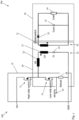
- FIG. 1 a block diagram of an exemplary embodiment of an isolated, primary side switched resonant converter 100 for supplying an LED load 34 is illustrated.
- Said converter 100 comprises an isolation barrier defining a primary side 61 and a secondary side 62, and means for detecting the falling zero crossing of a current through a primary side resonance circuit of the converter 100 exemplarily in the form of a shunt resistor 24.
- the converter 100 comprises a not explicitly shown control circuit arranged for varying the power transmitted by the converter 100 by modulating HF (high frequency) switching operations, preferably with constant frequencies, of at least primary side switch, such as the high side switch 11 and/or the low side switch 12, of the converter 100 with LF (low frequency) PWM (pulse width modulation) pulses with variable duty cycle.
- HF high frequency
- LF low frequency
- PWM pulse width modulation
- the converter 100 is void of means for detecting the rising zero crossings of the current through the primary side resonance circuit of the converter 100. Additionally, the control circuit is designed to calculate the timing of the rising zero crossings of the current through the primary side resonance circuit of the converter 100.
- control circuit is arranged to control the trailing high/low transition of each PWM pulse to be during one of the rising/falling zero crossings.
- the extrapolation is based on the modulation of the HF switching operations.
- control circuit may preferably be designed to not limit the leading low/high transition of each PWM pulse to the rising/falling zero crossing periods.
- the converter 100 is any of a half bridge LLC, half bridge LCC or resonant flyback converter.
- the converter 100 especially is a resonant hybrid flyback converter.
- Hybrid flyback can especially be understood as a "half-bridge circuit supplying a flyback resonant tank”.
- control circuit has a dimming signal input.
- Fig. 1 also depicts a LED lighting module 200 comprising the above-mentioned converter 100 and the above-mentioned LED load 34 supplied directly or indirectly by said converter 100. Said further details are especially explained in the light that the converter 100 exemplarily is a resonant hybrid flyback converter as already mentioned above.
- the converter or the resonant hybrid flyback converter 100 exemplarily comprises a half-bridge 10, and a flyback resonant tank 20 comprising a transformer with a primary side 61 and a secondary side 62.
- the half-bridge 10 is configured to supply said primary side 61.
- the resonant hybrid flyback converter 100 is configured to sense a primary-side current in the flyback resonant tank 20 or to detect the falling zero crossing of the current through the primary side resonance circuit of the converter 100, respectively.
- said sensing can be used for an overcurrent detection.
- said control circuit can be a control unit especially controlling the operation of the high side switch 11 and/or the low side switch 12 of the half-bridge 10 and/or being supplied with a feedback signal ("sensing" or reference sign 25, respectively) from a sensing circuit (Rshunt or reference sign 24, respectively) configured to sense a primary-side current in the flyback resonant tank 20.
- a feedback signal (“sensing" or reference sign 25, respectively) from a sensing circuit (Rshunt or reference sign 24, respectively) configured to sense a primary-side current in the flyback resonant tank 20.
- control unit can also be a control and/or processing unit.
- control and/or processing unit will be used, wherein the corresponding features can analogously apply for the control unit 70. Nevertheless, it is also possible that such a control and/or processing unit is employed in addition to the control unit 70.
- the above-mentioned half-bridge 10 comprises a high-side switch 11, exemplarily in the form of a first field-effect transistor, and a low-side switch 12, exemplarily in the form of a second field-effect transistor.
- said field-effect transistors 11 and 12 are exemplarily of an n-channel enhancement type.
- a first terminal, exemplarily a drain terminal, of the first field-effect transistor 11 is connected to a voltage potential, exemplarily a supply voltage
- a second terminal, exemplarily a source terminal, of the first field-effect transistor 11 is connected to a first terminal, exemplarily a drain terminal, of the second field-effect transistor 12.
- a second terminal, exemplarily a source terminal, of said second field-effect transistor 12 is connected to a voltage potential, especially another voltage potential, exemplarily ground.
- a third terminal, exemplarily a gate terminal, of the first field-effect transistor 11 may especially be connected to the above-mentioned control circuit or control unit, respectively.
- a third terminal, exemplarily a gate terminal, of the second field-effect transistor 12 may especially be connected to the above-mentioned control circuit or control unit, respectively.
- the above-mentioned primary side 61 comprises a series connection of a leakage inductance 22, which can be optional or omitted, respectively, a corresponding transformer main inductance 21 and a capacitance 23, exemplarily a resonance capacitor.
- the corresponding primary-side current especially flows through said series connection.
- the flyback resonant tank 20, exemplarily the primary side 61 comprises a resistance, exemplarily the shunt resistor 24 providing a sensing voltage in accordance with the corresponding primary-side current.
- the shunt resistor 24 is connected in series with the low side switch 12 of the half bridge 10 of the converter 100.
- shunt resistor 24 can then in addition also be used for other monitoring purposes, such as over current or (indirect) over voltage conditions.
- the series connection further comprises said resistance or said shunt resistor 24 providing the sensing voltage in accordance with the corresponding primary-side current, respectively.
- the above-mentioned first terminal, exemplarily the drain terminal, of the second field-effect transistor 12 is connected to a first terminal of the leakage inductance 22, whereas a second terminal of said leakage inductance 22 is connected to a first terminal of the transformer main inductance 21.
- the leakage inductance 22 is omitted, it is noted that the first terminal of the second field-effect transistor 12 is connected to said first terminal of the transformer main inductance 21.
- a second terminal of the transformer main inductance 21 is connected to a first terminal of the above-mentioned capacitance 23.
- the low side switch 12 of the half bridge 10 is connected to a first terminal of the shunt resistor 24, whereas a second terminal of said shunt resistor 24 providing the sensing voltage in accordance with the corresponding primary-side current is connected to a voltage potential, exemplarily ground.
- the first terminal of the shunt resistor 24 is connected to a sensing terminal 25.
- the resonant hybrid flyback converter 100 further comprises supplying means 30 being configured to be supplied by the secondary side 62 and to supply the LED lighting means or the load 34, respectively.
- the supplying means 30 comprise a switch and/or a diode, exemplarily a diode 32, and a capacitance, exemplarily an output capacitor 33.
- the capacitance 33 is exemplarily connected in parallel to the load 34, whereas the diode 32 is exemplarily connected in series to the load 34.
- a first terminal of a transformer secondary inductance 31 is connected to a first terminal, exemplarily an anode terminal, of the diode 32, whereas a second terminal, exemplarily a cathode terminal, of said diode 32 is connected to a first terminal of the capacitance 33 and to a first terminal of the load 34.
- a second terminal of the transformer secondary inductance 31 is connected to a second terminal of the capacitance 33 and to a second terminal of the load 34.
- Fig. 2 shows a flow chart of an embodiment of the inventive method for operating an isolated, primary side switched resonant converter supplying an LED load.
- a first step 301 comprises varying the power transmitted by the converter by modulating HF switching operations, preferably with constant frequencies, of at least primary side switch of the converter with LF PWM pulses with variable duty cycle.
- a second step 302 comprises detecting the falling zero crossing of a current through a primary side resonance circuit of the converter.
- a third step 303 comprises calculating the timing of the rising zero crossings of the current through the primary side resonance circuit of the converter.
- a fourth step 304 comprises controlling the trailing high/low transition of each PWM pulse to be during one of the rising/falling zero crossings.
- step 302 it is noted that it might be advantageous if said falling zero crossing is detected with the aid of a resistor, preferably a shunt resistor.
- said resistor preferably said shunt resistor, is connected in series with a low side switch of a half bridge of the converter.
- step 303 it is noted that it might be advantageous if calculating the timing of the rising zero crossings comprises an extrapolation or performing an extrapolation, respectively.
- the extrapolation is based on the frequency of the HF switching operations or the modulation of the HF switching operations.
- the rising zero cross will occur one half HF switching cycle after the falling zero cross.
Landscapes
- Engineering & Computer Science (AREA)
- Power Engineering (AREA)
- Dc-Dc Converters (AREA)
- Circuit Arrangement For Electric Light Sources In General (AREA)
Abstract
Description
- The invention relates to isolated, primary side switched resonant converters for supplying a LED load, a LED lighting module comprising such converters and a LED load, a method for operating an isolated, primary side switched resonant converter supplying an LED load, and an integrated control circuit implementing such a method.
- Resonant converters are preferably operated with a frequency close to their resonant frequency. A change of output current or voltage is performed by modulating high frequency pulses of the resonant converter with a low frequency pulse width modulation PWM signal. By adjusting the duty cycle of the PWM signal, a dimming of the power transmitted by the converter, and thus the resulting current through the load can be achieved.
- When the converter is operated with a frequency different from the resonant frequency, typically higher than the resonance frequency, a switching-off of the high frequency pulses of the resonant converter does not necessary lead to an immediate switching off of the power transmission between the primary converter side and the secondary converter side of the converter. Rather, it can lead to an ongoing power transmission with a relatively high peak and a resulting ripple in the output current supplied to the load. This leads to a sub-optimal switching behavior with regard to output current control.
- For instance,
EP 3 907 870 A1 discloses a resonant converter comprising a primary converter side, comprising a converter switching circuit, a secondary converter side, and a controller. The controller is configured to operate the converter switching circuit using pulse width modulation, for regulating a power transfer from the primary converter side to the secondary converter side. The resonant converter comprises an overshoot protection circuit connected to the primary converter side and/or to the controller. The overshoot protection circuit is configured to, and as switch-off event, effectively stop a power transfer from the primary converter side to the secondary converter side at the end of a pulse width modulation pulse. Furthermore, the overshoot protection circuit comprises a zero crossing detection circuit. The zero crossing detection circuit comprises a current measuring coil, which is coupled to the first resonant inductor, and a current measuring circuit, connected to the current measuring coil. Disadvantageously, due to an expensive design especially in the sense of the required current measuring coil, said resonant converter does not allow for a particularly high cost-efficiency in the context of a very accurate output current control. - Accordingly, the object of the invention is to provide an improved power converter, which allows not only for a very accurate output current control but also for a particularly high cost-efficiency.
- The object is solved by the features of the independent claims. Additional features of the invention are provided in the dependent claims.
- According to a first aspect of the invention, an isolated, primary side switched resonant converter for supplying an LED load is provided. Said converter comprises an isolation barrier defining a primary side and a secondary side, a control circuit arranged for varying the power transmitted by the converter by modulating HF switching operations, preferably with constant frequencies, of at least primary side switch of the converter with LF PWM pulses with variable duty cycle, and means for detecting the falling zero crossing of a current through a primary side resonance circuit of the converter. In this context, the converter is void of means for detecting the rising zero crossings of the current through the primary side resonance circuit of the converter. In addition to this, the control circuit is arranged to control the trailing high/low transition of each PWM pulse to be during one of the rising/falling zero crossings. Advantageously, a particularly high cost-efficiency can be ensured especially in the context of a very accurate output current control.
- According to a second aspect of the invention, an isolated, primary side switched resonant converter for supplying an LED load is provided. Said converter comprises an isolation barrier defining a primary side and a secondary side, a control circuit arranged for varying the power transmitted by the converter by modulating HF switching operations, preferably with constant frequencies, of at least primary side switch of the converter with LF PWM pulses with variable duty cycle, and means for detecting the falling zero crossings of a current through a primary side resonance circuit of the converter. In this context, the control circuit is designed to calculate the timing of the rising zero crossings of the current through the primary side resonance circuit of the converter. In addition to this, the control circuit is arranged to control the trailing high/low transition of each PWM pulse to be during one of the rising/falling zero crossings. Advantageously, a particularly high cost-efficiency can be ensured especially in the context of a very accurate output current control.
- According to an implementation form of the first aspect of the invention, the means for detecting the falling zero crossing comprises or is a resistor, preferably a shunt resistor. Advantageously, for instance, complexity can be reduced, thereby increasing cost-efficiency. Further advantageously, the resistor, preferably the shunt resistor, can be connected in series to a low side switch of a half bridge of the converter. Note that the shunt can then in addition also be used for other monitoring purposes, such as over current or (indirect) over voltage conditions.
- According to an implementation form of the second aspect of the invention, the means for detecting the falling zero crossing comprises or is a resistor, preferably a shunt resistor. Advantageously, for example, complexity can be reduced, which leads to an increased cost-efficiency. Further advantageously, the resistor, preferably the shunt resistor, can be connected in series to a low side switch of a half bridge of the converter.
- According to further implementation form of the first aspect of the invention or of the second aspect of the invention, respectively, calculating the timing of the rising zero crossings comprises an extrapolation. Advantageously, for instance, the timing of the rising zero crossing can be calculated in a particularly cost-efficient manner.
- According to further implementation form of the first aspect of the invention or of the second aspect of the invention, respectively, the extrapolation is based on the modulation of the HF switching operations. Advantageously, for example, complexity of extrapolation can be reduced, thereby increasing cost-efficiency.
- According to further implementation form of the first aspect of the invention or of the second aspect of the invention, respectively, the control circuit is designed to not limit the leading low/high transition of each PWM pulse to the rising/falling zero crossing periods. Advantageously, for instance, the converter can further be improved.
- According to further implementation form of the first aspect of the invention or of the second aspect of the invention, respectively, the converter is any of a half bridge LLC, half bridge LCC or resonant flyback converter. Advantageously, for example, a high flexibility can be ensured, which leads to an increased cost-efficiency.
- According to further implementation form of the first aspect of the invention or of the second aspect of the invention, respectively, the control circuit has a dimming signal input. Advantageously, for instance, accuracy and cost-efficiency can further be increased.
- According to a third aspect of the invention, a LED lighting module is provided. Said LED lighting module comprises a converter according to the first aspect of the invention or the second aspect of the invention, or any of its implementation forms, respectively, and a LED load supplied directly or indirectly by said converter. Advantageously, a particularly high cost-efficiency can be ensured especially in the context of a very accurate output current control.
- According to a fourth aspect of the invention, a method for operating an isolated, primary side switched resonant converter supplying an LED load is provided. Said method comprises the steps of varying the power transmitted by the converter by modulating HF switching operations, preferably with constant frequencies, of at least primary side switch of the converter with LF PWM pulses with variable duty cycle, detecting the falling zero crossing of a current through a primary side resonance circuit of the converter, calculating the timing of the rising zero crossings of the current through the primary side resonance circuit of the converter, and controlling the trailing high/low transition of each PWM pulse to be during one of the rising/falling zero crossings. Advantageously, a particularly high cost-efficiency can be ensured especially in the context of a very accurate output current control.
- According to an implementation form of the fourth aspect of the invention, the falling zero crossing is detected with the aid of a resistor, preferably a shunt resistor. Advantageously, for instance, complexity can be reduced, thereby increasing cost-efficiency. Further advantageously, the resistor, preferably the shunt resistor, can be connected in series to a low side switch of a half bridge of the converter.
- According to a further implementation form of the fourth aspect of the invention, calculating the timing of the rising zero crossings comprises performing an extrapolation. Advantageously, for example, the timing of the rising zero crossing can be calculated in a particularly cost-efficient manner.
- According to a further implementation form of the fourth aspect of the invention, the extrapolation is based on the modulation of the HF switching operations. Advantageously, for instance, complexity of extrapolation can be reduced, thereby increasing cost-efficiency.
- According to a fifth aspect of the invention, an integrated control circuit arranged for implementing the steps of the fourth aspect of the invention or any of its implementation forms, respectively, is provided. Advantageously, a particularly high cost-efficiency can be ensured especially in the context of a very accurate output current control.
- Exemplary embodiments of the invention are now further explained with respect to the drawings by way of example only, and not for limitation. In the drawings:
- Fig. 1
- shows an exemplary embodiment of the first aspect of the invention or the second aspect of the invention, respectively, in combination with the third aspect of the invention; and
- Fig. 2
- shows a flow chart of an embodiment of the fourth aspect of the invention.
- With respect to
Fig. 1 , a block diagram of an exemplary embodiment of an isolated, primary side switchedresonant converter 100 for supplying anLED load 34 is illustrated. - Said
converter 100 comprises an isolation barrier defining aprimary side 61 and asecondary side 62, and means for detecting the falling zero crossing of a current through a primary side resonance circuit of theconverter 100 exemplarily in the form of ashunt resistor 24. - With respect to said
shunt resistor 24, it is noted that it might generally be advantageous if said shunt resistor is connected in series with thelow side switch 12 of thehalf bridge 10 of theconverter 100. - Furthermore, the
converter 100 comprises a not explicitly shown control circuit arranged for varying the power transmitted by theconverter 100 by modulating HF (high frequency) switching operations, preferably with constant frequencies, of at least primary side switch, such as thehigh side switch 11 and/or thelow side switch 12, of theconverter 100 with LF (low frequency) PWM (pulse width modulation) pulses with variable duty cycle. - In this context, the
converter 100 is void of means for detecting the rising zero crossings of the current through the primary side resonance circuit of theconverter 100. Additionally, the control circuit is designed to calculate the timing of the rising zero crossings of the current through the primary side resonance circuit of theconverter 100. - Moreover, it is noted that the control circuit is arranged to control the trailing high/low transition of each PWM pulse to be during one of the rising/falling zero crossings.
- It is further noted that it might be advantageous if the above-mentioned calculating the timing of the rising zero crossings comprises an extrapolation.
- In this context, it might be advantageous if the extrapolation is based on the modulation of the HF switching operations.
- Furthermore, the control circuit may preferably be designed to not limit the leading low/high transition of each PWM pulse to the rising/falling zero crossing periods.
- It is further noted that it might be advantageous if the
converter 100 is any of a half bridge LLC, half bridge LCC or resonant flyback converter. - Exemplarily, the
converter 100 especially is a resonant hybrid flyback converter. "Hybrid flyback" can especially be understood as a "half-bridge circuit supplying a flyback resonant tank". - With respect to the above-mentioned control circuit, it is noted that it might be advantageous if the control circuit has a dimming signal input.
- Before some further details of
Fig. 1 are explained in the following, it is noted that saidFig. 1 also depicts aLED lighting module 200 comprising the above-mentionedconverter 100 and the above-mentionedLED load 34 supplied directly or indirectly by saidconverter 100. Said further details are especially explained in the light that theconverter 100 exemplarily is a resonant hybrid flyback converter as already mentioned above. - As it can be seen from
Fig. 1 , the converter or the resonanthybrid flyback converter 100, respectively, exemplarily comprises a half-bridge 10, and a flybackresonant tank 20 comprising a transformer with aprimary side 61 and asecondary side 62. - In this context, the half-
bridge 10 is configured to supply saidprimary side 61. Furthermore, the resonanthybrid flyback converter 100 is configured to sense a primary-side current in the flybackresonant tank 20 or to detect the falling zero crossing of the current through the primary side resonance circuit of theconverter 100, respectively. - Advantageously, it is noted that said sensing can be used for an overcurrent detection.
- With respect to the above-mentioned control circuit, it is noted that said control circuit can be a control unit especially controlling the operation of the
high side switch 11 and/or thelow side switch 12 of the half-bridge 10 and/or being supplied with a feedback signal ("sensing" orreference sign 25, respectively) from a sensing circuit (Rshunt orreference sign 24, respectively) configured to sense a primary-side current in the flybackresonant tank 20. - With respect to said control unit, it is noted that the control unit can also be a control and/or processing unit. In the following, the term "control and/or processing unit" will be used, wherein the corresponding features can analogously apply for the control unit 70. Nevertheless, it is also possible that such a control and/or processing unit is employed in addition to the control unit 70.
- The above-mentioned half-
bridge 10 comprises a high-side switch 11, exemplarily in the form of a first field-effect transistor, and a low-side switch 12, exemplarily in the form of a second field-effect transistor. - For the sake of completeness, with respect to said field-
effect transistors - In this context, a first terminal, exemplarily a drain terminal, of the first field-
effect transistor 11 is connected to a voltage potential, exemplarily a supply voltage, whereas a second terminal, exemplarily a source terminal, of the first field-effect transistor 11 is connected to a first terminal, exemplarily a drain terminal, of the second field-effect transistor 12. Furthermore, a second terminal, exemplarily a source terminal, of said second field-effect transistor 12 is connected to a voltage potential, especially another voltage potential, exemplarily ground. - It is further noted that a third terminal, exemplarily a gate terminal, of the first field-
effect transistor 11 may especially be connected to the above-mentioned control circuit or control unit, respectively. In addition to this or as an alternative, a third terminal, exemplarily a gate terminal, of the second field-effect transistor 12 may especially be connected to the above-mentioned control circuit or control unit, respectively. - Moreover, the above-mentioned
primary side 61 comprises a series connection of aleakage inductance 22, which can be optional or omitted, respectively, a corresponding transformermain inductance 21 and acapacitance 23, exemplarily a resonance capacitor. In this context, the corresponding primary-side current especially flows through said series connection. - Furthermore, especially in the context of sensing the corresponding primary-side current, the flyback
resonant tank 20, exemplarily theprimary side 61, comprises a resistance, exemplarily theshunt resistor 24 providing a sensing voltage in accordance with the corresponding primary-side current. Preferably theshunt resistor 24 is connected in series with thelow side switch 12 of thehalf bridge 10 of theconverter 100. - Note that the
shunt resistor 24 can then in addition also be used for other monitoring purposes, such as over current or (indirect) over voltage conditions. - Exemplarily, in accordance with
Fig. 1 , the series connection further comprises said resistance or saidshunt resistor 24 providing the sensing voltage in accordance with the corresponding primary-side current, respectively. - Moreover, the above-mentioned first terminal, exemplarily the drain terminal, of the second field-
effect transistor 12 is connected to a first terminal of theleakage inductance 22, whereas a second terminal of saidleakage inductance 22 is connected to a first terminal of the transformermain inductance 21. For the case that theleakage inductance 22 is omitted, it is noted that the first terminal of the second field-effect transistor 12 is connected to said first terminal of the transformermain inductance 21. - In addition to this, a second terminal of the transformer
main inductance 21 is connected to a first terminal of the above-mentionedcapacitance 23. - The
low side switch 12 of thehalf bridge 10 is connected to a first terminal of theshunt resistor 24, whereas a second terminal of saidshunt resistor 24 providing the sensing voltage in accordance with the corresponding primary-side current is connected to a voltage potential, exemplarily ground. - In further addition to this, the first terminal of the
shunt resistor 24 is connected to asensing terminal 25. - As it can further be seen from
Fig. 1 , the resonanthybrid flyback converter 100 further comprises supplying means 30 being configured to be supplied by thesecondary side 62 and to supply the LED lighting means or theload 34, respectively. - In this context, the supplying
means 30 comprise a switch and/or a diode, exemplarily adiode 32, and a capacitance, exemplarily anoutput capacitor 33. - Furthermore, the
capacitance 33 is exemplarily connected in parallel to theload 34, whereas thediode 32 is exemplarily connected in series to theload 34. - In particular, a first terminal of a transformer
secondary inductance 31 is connected to a first terminal, exemplarily an anode terminal, of thediode 32, whereas a second terminal, exemplarily a cathode terminal, of saiddiode 32 is connected to a first terminal of thecapacitance 33 and to a first terminal of theload 34. - In addition to this, a second terminal of the transformer
secondary inductance 31 is connected to a second terminal of thecapacitance 33 and to a second terminal of theload 34. - Finally,
Fig. 2 shows a flow chart of an embodiment of the inventive method for operating an isolated, primary side switched resonant converter supplying an LED load. Afirst step 301 comprises varying the power transmitted by the converter by modulating HF switching operations, preferably with constant frequencies, of at least primary side switch of the converter with LF PWM pulses with variable duty cycle. Furthermore, asecond step 302 comprises detecting the falling zero crossing of a current through a primary side resonance circuit of the converter. Moreover, athird step 303 comprises calculating the timing of the rising zero crossings of the current through the primary side resonance circuit of the converter. In addition to this, afourth step 304 comprises controlling the trailing high/low transition of each PWM pulse to be during one of the rising/falling zero crossings. - With respect to the above-mentioned falling zero crossing according to step 302, it is noted that it might be advantageous if said falling zero crossing is detected with the aid of a resistor, preferably a shunt resistor.
- It is further noted that it might be advantageous if said resistor, preferably said shunt resistor, is connected in series with a low side switch of a half bridge of the converter.
- With respect to the above-mentioned
step 303, it is noted that it might be advantageous if calculating the timing of the rising zero crossings comprises an extrapolation or performing an extrapolation, respectively. - With respect to said extrapolation, it is noted that it might be advantageous if the extrapolation is based on the frequency of the HF switching operations or the modulation of the HF switching operations. The rising zero cross will occur one half HF switching cycle after the falling zero cross.
- While various embodiments of the present invention have been described above, it should be understood that they have been presented by way of example only, and not limitation. Numerous changes to the disclosed embodiments can be made in accordance with the disclosure herein without departing from the spirit or scope of the invention. Thus, the breadth and scope of the present invention should not be limited by any of the above described embodiments. Rather, the scope of the invention should be defined in accordance with the following claims and their equivalents.
- Although the invention has been illustrated and described with respect to one or more implementations, equivalent alterations and modifications will occur to others skilled in the art upon the reading and understanding of this specification and the annexed drawings. In addition, while a particular feature of the invention may have been disclosed with respect to only one of several implementations, such feature may be combined with one or more other features of the other implementations as may be desired and advantageous for any given or particular application.
Claims (15)
- Isolated, primary side switched resonant converter (100) for supplying a LED load (34),
comprising:- an isolation barrier defining a primary side (61) and a secondary side (62),- a control circuit arranged for varying the power transmitted by the converter by modulating HF switching operations, preferably with constant frequencies, of at least primary side switch (11, 12) of the converter (100) with LF PWM pulses with variable duty cycle,- means for detecting (24) the falling zero crossing of a current through a primary side resonance circuit of the converter (100),wherein the converter (100) is void of means for detecting the rising zero crossings of the current through the primary side resonance circuit of the converter (100), and wherein the control circuit is arranged to control the trailing high/low transition of each PWM pulse to be during one of the rising/falling zero crossings. - Isolated, primary side switched resonant converter (100) for supplying a LED load (34),
comprising:- an isolation barrier defining a primary side (61) and a secondary side (62),- a control circuit arranged for varying the power transmitted by the converter (100) by modulating HF switching operations, preferably with constant frequencies, of at least primary side switch (11, 12) of the converter (100) with LF PWM pulses with variable duty cycle,- means for detecting (24) the falling zero crossings of a current through a primary side resonance circuit of the converter (100),wherein the control circuit is designed to calculate the timing of the rising zero crossings of the current through the primary side resonance circuit of the converter (100), andwherein the control circuit is arranged to control the trailing high/low transition of each PWM pulse to be during one of the rising/falling zero crossings. - The converter (100) of claim 1 or 2,
wherein the means for detecting (24) the falling zero crossing comprises or is a resistor, preferably a shunt resistor. - The converter (100) of claim 1 or 2,
wherein the means for detecting (24) the falling zero crossing comprises a shunt resistor arranged between a low side switch of a half-bridge converter and ground potential. - The converter (100) of claim 2 or 4,
wherein calculating the timing of the rising zero crossings comprises an extrapolation. - The converter (100) of claim 5,
wherein the extrapolation is based on the frequency of the HF switching operations. - The converter (100) of any of the preceding claims,
wherein the control circuit is designed to not limit the leading low/high transition of each PWM pulse to the rising/falling zero crossing periods. - The converter (100) of any of the preceding claims, wherein the converter is any of a half bridge LLC, half bridge LCC or resonant flyback converter.
- The converter (100) of any of the preceding claims, wherein the control circuit has a dimming signal input.
- A LED lighting module (200) comprising a converter (100) according to any of the preceding claims and a LED load (34) supplied directly or indirectly by said converter.
- A method for operating an isolated, primary side switched resonant converter supplying an LED load, comprising the steps of:- varying (301) the power transmitted by the converter by modulating HF switching operations, preferably with constant frequencies, of at least primary side switch of the converter with LF PWM pulses with variable duty cycle,- detecting (302) the falling zero crossing of a current through a primary side resonance circuit of the converter,- calculating (303) the timing of the rising zero crossings of the current through the primary side resonance circuit of the converter, and- controlling (304) the trailing high/low transition of each PWM pulse to be during one of the rising/falling zero crossings.
- The method of claim 11,
wherein the falling zero crossing is detected with the aid of a resistor, preferably a shunt resistor. - The method of claim 11 or 12,
wherein calculating the timing of the rising zero crossings comprises performing an extrapolation. - The method of claim 13,
wherein the extrapolation is based on the modulation of the HF switching operations. - An integrated control circuit arranged for implementing the steps of any of the claims 11 to 14.
Priority Applications (2)
| Application Number | Priority Date | Filing Date | Title |
|---|---|---|---|
| EP23172469.1A EP4462665B1 (en) | 2023-05-10 | 2023-05-10 | Isolated, primary side switched resonant conversion for supplying a led load |
| PCT/EP2024/060233 WO2024231048A1 (en) | 2023-05-10 | 2024-04-16 | Improved isolated, primary side switched resonant converter for supplying a led load |
Applications Claiming Priority (1)
| Application Number | Priority Date | Filing Date | Title |
|---|---|---|---|
| EP23172469.1A EP4462665B1 (en) | 2023-05-10 | 2023-05-10 | Isolated, primary side switched resonant conversion for supplying a led load |
Publications (2)
| Publication Number | Publication Date |
|---|---|
| EP4462665A1 true EP4462665A1 (en) | 2024-11-13 |
| EP4462665B1 EP4462665B1 (en) | 2026-03-11 |
Family
ID=86331202
Family Applications (1)
| Application Number | Title | Priority Date | Filing Date |
|---|---|---|---|
| EP23172469.1A Active EP4462665B1 (en) | 2023-05-10 | 2023-05-10 | Isolated, primary side switched resonant conversion for supplying a led load |
Country Status (2)
| Country | Link |
|---|---|
| EP (1) | EP4462665B1 (en) |
| WO (1) | WO2024231048A1 (en) |
Citations (3)
| Publication number | Priority date | Publication date | Assignee | Title |
|---|---|---|---|---|
| US20150002032A1 (en) * | 2011-12-23 | 2015-01-01 | Tridonic Gmbh & Co Kg | Led converter with adaptive pfc and resonant converter |
| US9960693B1 (en) * | 2016-10-27 | 2018-05-01 | Infineon Technologies Austria Ag | Control of switching frequency based on difference in phase relations |
| EP3907870A1 (en) | 2020-05-04 | 2021-11-10 | Tridonic GmbH & Co. KG | Power converter with overshoot protection |
-
2023
- 2023-05-10 EP EP23172469.1A patent/EP4462665B1/en active Active
-
2024
- 2024-04-16 WO PCT/EP2024/060233 patent/WO2024231048A1/en not_active Ceased
Patent Citations (3)
| Publication number | Priority date | Publication date | Assignee | Title |
|---|---|---|---|---|
| US20150002032A1 (en) * | 2011-12-23 | 2015-01-01 | Tridonic Gmbh & Co Kg | Led converter with adaptive pfc and resonant converter |
| US9960693B1 (en) * | 2016-10-27 | 2018-05-01 | Infineon Technologies Austria Ag | Control of switching frequency based on difference in phase relations |
| EP3907870A1 (en) | 2020-05-04 | 2021-11-10 | Tridonic GmbH & Co. KG | Power converter with overshoot protection |
Also Published As
| Publication number | Publication date |
|---|---|
| EP4462665B1 (en) | 2026-03-11 |
| WO2024231048A1 (en) | 2024-11-14 |
Similar Documents
| Publication | Publication Date | Title |
|---|---|---|
| US8188617B2 (en) | Current balancing apparatus, current balancing method, and power supply apparatus | |
| CN120582463A (en) | Power converter controller, power converter, and method for operating a power converter | |
| EP2432105B1 (en) | Power factor correcting current resonance converter | |
| US9209703B2 (en) | Control device for a rectifier of a switching converter | |
| JP6932633B2 (en) | Switching power supply | |
| US8724352B2 (en) | Power supply apparatus driving circuit, power supply apparatus driving integrated circuit, and power supply apparatus | |
| KR20120038466A (en) | Low cost power supply circuit and method | |
| JP2021090264A (en) | Gate drive circuit and control circuit of switching circuit, and switching power supply | |
| CN111224551B (en) | Power Converters | |
| US10826402B1 (en) | Methods and systems of controlling switching frequency of LLC resonant power converters | |
| US8421505B2 (en) | Drive circuit for semiconductor switching element | |
| CN115833610B (en) | Power supply conversion circuit and electronic device | |
| US20180076713A1 (en) | Switch drive circuit and switching power supply device using same | |
| US12160230B2 (en) | Switching circuit apparatus capable of controlling multiple switching elements to synchronously turn on and off with bootstrap circuit | |
| EP4462665B1 (en) | Isolated, primary side switched resonant conversion for supplying a led load | |
| EP3907870A1 (en) | Power converter with overshoot protection | |
| EP4387069A1 (en) | Resonant hybrid flyback converter for a led-based load | |
| US9426854B1 (en) | Electronic driver for controlling an illumination device | |
| CN110168890B (en) | Control circuit with two-point regulator for regulating clock-driven converter | |
| EP4612784A1 (en) | Resonant hybrid flyback converter for a led-based load | |
| EP4387395A1 (en) | Resonant hybrid flyback converter for a led-based load | |
| US11444531B2 (en) | Voltage converter | |
| EP3766308B1 (en) | Power supplier circuit, controlling method and electronic equipment | |
| EP3926808A1 (en) | A synchronous flyback converter | |
| EP4560901A1 (en) | Switching power supply, and method of operating the same |
Legal Events
| Date | Code | Title | Description |
|---|---|---|---|
| PUAI | Public reference made under article 153(3) epc to a published international application that has entered the european phase |
Free format text: ORIGINAL CODE: 0009012 |
|
| STAA | Information on the status of an ep patent application or granted ep patent |
Free format text: STATUS: THE APPLICATION HAS BEEN PUBLISHED |
|
| AK | Designated contracting states |
Kind code of ref document: A1 Designated state(s): AL AT BE BG CH CY CZ DE DK EE ES FI FR GB GR HR HU IE IS IT LI LT LU LV MC ME MK MT NL NO PL PT RO RS SE SI SK SM TR |
|
| STAA | Information on the status of an ep patent application or granted ep patent |
Free format text: STATUS: REQUEST FOR EXAMINATION WAS MADE |
|
| 17P | Request for examination filed |
Effective date: 20250207 |
|
| GRAP | Despatch of communication of intention to grant a patent |
Free format text: ORIGINAL CODE: EPIDOSNIGR1 |
|
| STAA | Information on the status of an ep patent application or granted ep patent |
Free format text: STATUS: GRANT OF PATENT IS INTENDED |
|
| RAP3 | Party data changed (applicant data changed or rights of an application transferred) |
Owner name: TRIDONIC GMBH & CO KG |
|
| GRAS | Grant fee paid |
Free format text: ORIGINAL CODE: EPIDOSNIGR3 |
|
| GRAA | (expected) grant |
Free format text: ORIGINAL CODE: 0009210 |
|
| STAA | Information on the status of an ep patent application or granted ep patent |
Free format text: STATUS: THE PATENT HAS BEEN GRANTED |
|
| INTG | Intention to grant announced |
Effective date: 20260108 |
|
| AK | Designated contracting states |
Kind code of ref document: B1 Designated state(s): AL AT BE BG CH CY CZ DE DK EE ES FI FR GB GR HR HU IE IS IT LI LT LU LV MC ME MK MT NL NO PL PT RO RS SE SI SK SM TR |
|
| REG | Reference to a national code |
Ref country code: CH Ref legal event code: F10 Free format text: ST27 STATUS EVENT CODE: U-0-0-F10-F00 (AS PROVIDED BY THE NATIONAL OFFICE) Effective date: 20260311 Ref country code: GB Ref legal event code: FG4D |
|
| P01 | Opt-out of the competence of the unified patent court (upc) registered |
Free format text: CASE NUMBER: UPC_APP_0005587_4462665/2026 Effective date: 20260216 |
|
| REG | Reference to a national code |
Ref country code: DE Ref legal event code: R096 Ref document number: 602023013225 Country of ref document: DE |
|
| REG | Reference to a national code |
Ref country code: IE Ref legal event code: FG4D |
|
| REG | Reference to a national code |
Ref country code: DE Ref legal event code: R084 Ref document number: 602023013225 Country of ref document: DE |
|
| PG25 | Lapsed in a contracting state [announced via postgrant information from national office to epo] |
Ref country code: RS Free format text: LAPSE BECAUSE OF FAILURE TO SUBMIT A TRANSLATION OF THE DESCRIPTION OR TO PAY THE FEE WITHIN THE PRESCRIBED TIME-LIMIT Effective date: 20260611 |
|
| PG25 | Lapsed in a contracting state [announced via postgrant information from national office to epo] |
Ref country code: ES Free format text: LAPSE BECAUSE OF FAILURE TO SUBMIT A TRANSLATION OF THE DESCRIPTION OR TO PAY THE FEE WITHIN THE PRESCRIBED TIME-LIMIT Effective date: 20260311 |
|
| PG25 | Lapsed in a contracting state [announced via postgrant information from national office to epo] |
Ref country code: GR Free format text: LAPSE BECAUSE OF FAILURE TO SUBMIT A TRANSLATION OF THE DESCRIPTION OR TO PAY THE FEE WITHIN THE PRESCRIBED TIME-LIMIT Effective date: 20260612 |
|
| REG | Reference to a national code |
Ref country code: LT Ref legal event code: MG9D |
|
| PG25 | Lapsed in a contracting state [announced via postgrant information from national office to epo] |
Ref country code: LT Free format text: LAPSE BECAUSE OF FAILURE TO SUBMIT A TRANSLATION OF THE DESCRIPTION OR TO PAY THE FEE WITHIN THE PRESCRIBED TIME-LIMIT Effective date: 20260311 |
|
| PGFP | Annual fee paid to national office [announced via postgrant information from national office to epo] |
Ref country code: DE Payment date: 20260522 Year of fee payment: 4 |
|
| PG25 | Lapsed in a contracting state [announced via postgrant information from national office to epo] |
Ref country code: NO Free format text: LAPSE BECAUSE OF FAILURE TO SUBMIT A TRANSLATION OF THE DESCRIPTION OR TO PAY THE FEE WITHIN THE PRESCRIBED TIME-LIMIT Effective date: 20260611 |
|
| PG25 | Lapsed in a contracting state [announced via postgrant information from national office to epo] |
Ref country code: FI Free format text: LAPSE BECAUSE OF FAILURE TO SUBMIT A TRANSLATION OF THE DESCRIPTION OR TO PAY THE FEE WITHIN THE PRESCRIBED TIME-LIMIT Effective date: 20260311 Ref country code: SE Free format text: LAPSE BECAUSE OF FAILURE TO SUBMIT A TRANSLATION OF THE DESCRIPTION OR TO PAY THE FEE WITHIN THE PRESCRIBED TIME-LIMIT Effective date: 20260311 |
|
| REG | Reference to a national code |
Ref country code: NL Ref legal event code: MP Effective date: 20260311 |
|
| PG25 | Lapsed in a contracting state [announced via postgrant information from national office to epo] |
Ref country code: HR Free format text: LAPSE BECAUSE OF FAILURE TO SUBMIT A TRANSLATION OF THE DESCRIPTION OR TO PAY THE FEE WITHIN THE PRESCRIBED TIME-LIMIT Effective date: 20260311 |
|
| PGFP | Annual fee paid to national office [announced via postgrant information from national office to epo] |
Ref country code: FR Payment date: 20260522 Year of fee payment: 4 |
|
| PG25 | Lapsed in a contracting state [announced via postgrant information from national office to epo] |
Ref country code: LV Free format text: LAPSE BECAUSE OF FAILURE TO SUBMIT A TRANSLATION OF THE DESCRIPTION OR TO PAY THE FEE WITHIN THE PRESCRIBED TIME-LIMIT Effective date: 20260311 |
|
| PG25 | Lapsed in a contracting state [announced via postgrant information from national office to epo] |
Ref country code: BG Free format text: LAPSE BECAUSE OF FAILURE TO SUBMIT A TRANSLATION OF THE DESCRIPTION OR TO PAY THE FEE WITHIN THE PRESCRIBED TIME-LIMIT Effective date: 20260311 |