EP4462661A1 - Motor controller and powertrain - Google Patents
Motor controller and powertrain Download PDFInfo
- Publication number
- EP4462661A1 EP4462661A1 EP24172153.9A EP24172153A EP4462661A1 EP 4462661 A1 EP4462661 A1 EP 4462661A1 EP 24172153 A EP24172153 A EP 24172153A EP 4462661 A1 EP4462661 A1 EP 4462661A1
- Authority
- EP
- European Patent Office
- Prior art keywords
- voltage
- power supply
- control
- conversion circuit
- bridge arm
- Prior art date
- Legal status (The legal status is an assumption and is not a legal conclusion. Google has not performed a legal analysis and makes no representation as to the accuracy of the status listed.)
- Pending
Links
Images



Classifications
-
- H—ELECTRICITY
- H02—GENERATION; CONVERSION OR DISTRIBUTION OF ELECTRIC POWER
- H02P—CONTROL OR REGULATION OF ELECTRIC MOTORS, ELECTRIC GENERATORS OR DYNAMO-ELECTRIC CONVERTERS; CONTROLLING TRANSFORMERS, REACTORS OR CHOKE COILS
- H02P27/00—Arrangements or methods for the control of AC motors characterised by the kind of supply voltage
- H02P27/04—Arrangements or methods for the control of AC motors characterised by the kind of supply voltage using variable-frequency supply voltage, e.g. inverter or converter supply voltage
- H02P27/06—Arrangements or methods for the control of AC motors characterised by the kind of supply voltage using variable-frequency supply voltage, e.g. inverter or converter supply voltage using DC to AC converters or inverters
-
- H—ELECTRICITY
- H02—GENERATION; CONVERSION OR DISTRIBUTION OF ELECTRIC POWER
- H02J—ELECTRIC POWER NETWORKS; CIRCUIT ARRANGEMENTS OR SYSTEMS FOR SUPPLYING OR DISTRIBUTING ELECTRIC POWER; SYSTEMS FOR STORING ELECTRIC ENERGY
- H02J1/00—Circuit arrangements for DC mains or DC distribution networks
- H02J1/08—Three-wire DC power distribution systems; Systems having more than three wires
- H02J1/082—DC supplies with two or more different DC voltage levels
-
- H—ELECTRICITY
- H02—GENERATION; CONVERSION OR DISTRIBUTION OF ELECTRIC POWER
- H02J—ELECTRIC POWER NETWORKS; CIRCUIT ARRANGEMENTS OR SYSTEMS FOR SUPPLYING OR DISTRIBUTING ELECTRIC POWER; SYSTEMS FOR STORING ELECTRIC ENERGY
- H02J3/00—Circuit arrangements for AC mains or AC distribution networks
- H02J3/007—Arrangements for selectively connecting one or more loads to one or more power sources or power lines
- H02J3/0075—Arrangements for selectively connecting one or more loads to one or more power sources or power lines for providing alternative feeding paths between load and source according to economic or energy efficiency considerations, e.g. economic dispatch
-
- H—ELECTRICITY
- H02—GENERATION; CONVERSION OR DISTRIBUTION OF ELECTRIC POWER
- H02J—ELECTRIC POWER NETWORKS; CIRCUIT ARRANGEMENTS OR SYSTEMS FOR SUPPLYING OR DISTRIBUTING ELECTRIC POWER; SYSTEMS FOR STORING ELECTRIC ENERGY
- H02J7/00—Circuit arrangements for charging or discharging batteries or for supplying loads from batteries
- H02J7/855—Circuit arrangements for charging or discharging batteries or for supplying loads from batteries with circuits adapted for supplying loads from the battery
-
- H—ELECTRICITY
- H02—GENERATION; CONVERSION OR DISTRIBUTION OF ELECTRIC POWER
- H02M—APPARATUS FOR CONVERSION BETWEEN AC AND AC, BETWEEN AC AND DC, OR BETWEEN DC AND DC, AND FOR USE WITH MAINS OR SIMILAR POWER SUPPLY SYSTEMS; CONVERSION OF DC OR AC INPUT POWER INTO SURGE OUTPUT POWER; CONTROL OR REGULATION THEREOF
- H02M1/00—Details of apparatus for conversion
- H02M1/0003—Details of control, feedback or regulation circuits
- H02M1/0006—Arrangements for supplying an adequate voltage to the control circuit of converters
-
- H—ELECTRICITY
- H02—GENERATION; CONVERSION OR DISTRIBUTION OF ELECTRIC POWER
- H02M—APPARATUS FOR CONVERSION BETWEEN AC AND AC, BETWEEN AC AND DC, OR BETWEEN DC AND DC, AND FOR USE WITH MAINS OR SIMILAR POWER SUPPLY SYSTEMS; CONVERSION OF DC OR AC INPUT POWER INTO SURGE OUTPUT POWER; CONTROL OR REGULATION THEREOF
- H02M1/00—Details of apparatus for conversion
- H02M1/32—Means for protecting converters other than automatic disconnection
-
- H—ELECTRICITY
- H02—GENERATION; CONVERSION OR DISTRIBUTION OF ELECTRIC POWER
- H02M—APPARATUS FOR CONVERSION BETWEEN AC AND AC, BETWEEN AC AND DC, OR BETWEEN DC AND DC, AND FOR USE WITH MAINS OR SIMILAR POWER SUPPLY SYSTEMS; CONVERSION OF DC OR AC INPUT POWER INTO SURGE OUTPUT POWER; CONTROL OR REGULATION THEREOF
- H02M1/00—Details of apparatus for conversion
- H02M1/36—Means for starting or stopping converters
-
- H—ELECTRICITY
- H02—GENERATION; CONVERSION OR DISTRIBUTION OF ELECTRIC POWER
- H02P—CONTROL OR REGULATION OF ELECTRIC MOTORS, ELECTRIC GENERATORS OR DYNAMO-ELECTRIC CONVERTERS; CONTROLLING TRANSFORMERS, REACTORS OR CHOKE COILS
- H02P29/00—Arrangements for regulating or controlling electric motors, appropriate for both AC and DC motors
- H02P29/02—Providing protection against overload without automatic interruption of supply
-
- H—ELECTRICITY
- H02—GENERATION; CONVERSION OR DISTRIBUTION OF ELECTRIC POWER
- H02P—CONTROL OR REGULATION OF ELECTRIC MOTORS, ELECTRIC GENERATORS OR DYNAMO-ELECTRIC CONVERTERS; CONTROLLING TRANSFORMERS, REACTORS OR CHOKE COILS
- H02P6/00—Arrangements for controlling synchronous motors or other dynamo-electric motors using electronic commutation dependent on the rotor position; Electronic commutators therefor
- H02P6/08—Arrangements for controlling the speed or torque of a single motor
- H02P6/085—Arrangements for controlling the speed or torque of a single motor in a bridge configuration
-
- B—PERFORMING OPERATIONS; TRANSPORTING
- B60—VEHICLES IN GENERAL
- B60L—PROPULSION OF ELECTRICALLY-PROPELLED VEHICLES; SUPPLYING ELECTRIC POWER FOR AUXILIARY EQUIPMENT OF ELECTRICALLY-PROPELLED VEHICLES; ELECTRODYNAMIC BRAKE SYSTEMS FOR VEHICLES IN GENERAL; MAGNETIC SUSPENSION OR LEVITATION FOR VEHICLES; MONITORING OPERATING VARIABLES OF ELECTRICALLY-PROPELLED VEHICLES; ELECTRIC SAFETY DEVICES FOR ELECTRICALLY-PROPELLED VEHICLES
- B60L2210/00—Converter types
- B60L2210/40—DC to AC converters
-
- B—PERFORMING OPERATIONS; TRANSPORTING
- B60—VEHICLES IN GENERAL
- B60L—PROPULSION OF ELECTRICALLY-PROPELLED VEHICLES; SUPPLYING ELECTRIC POWER FOR AUXILIARY EQUIPMENT OF ELECTRICALLY-PROPELLED VEHICLES; ELECTRODYNAMIC BRAKE SYSTEMS FOR VEHICLES IN GENERAL; MAGNETIC SUSPENSION OR LEVITATION FOR VEHICLES; MONITORING OPERATING VARIABLES OF ELECTRICALLY-PROPELLED VEHICLES; ELECTRIC SAFETY DEVICES FOR ELECTRICALLY-PROPELLED VEHICLES
- B60L3/00—Electric devices on electrically-propelled vehicles for safety purposes; Monitoring operating variables, e.g. speed, deceleration or energy consumption
- B60L3/0023—Detecting, eliminating, remedying or compensating for drive train abnormalities, e.g. failures within the drive train
- B60L3/003—Detecting, eliminating, remedying or compensating for drive train abnormalities, e.g. failures within the drive train relating to inverters
-
- H—ELECTRICITY
- H02—GENERATION; CONVERSION OR DISTRIBUTION OF ELECTRIC POWER
- H02J—ELECTRIC POWER NETWORKS; CIRCUIT ARRANGEMENTS OR SYSTEMS FOR SUPPLYING OR DISTRIBUTING ELECTRIC POWER; SYSTEMS FOR STORING ELECTRIC ENERGY
- H02J1/00—Circuit arrangements for DC mains or DC distribution networks
- H02J1/10—Parallel operation of DC sources
- H02J1/108—Parallel operation of DC sources having arrangements for blocking reverse current flow, e.g. using diodes
-
- H—ELECTRICITY
- H02—GENERATION; CONVERSION OR DISTRIBUTION OF ELECTRIC POWER
- H02J—ELECTRIC POWER NETWORKS; CIRCUIT ARRANGEMENTS OR SYSTEMS FOR SUPPLYING OR DISTRIBUTING ELECTRIC POWER; SYSTEMS FOR STORING ELECTRIC ENERGY
- H02J2105/00—Networks for supplying or distributing electric power characterised by their spatial reach or by the load
- H02J2105/30—Networks for supplying or distributing electric power characterised by their spatial reach or by the load the load networks being external to vehicles, i.e. exchanging power with vehicles
- H02J2105/33—Networks for supplying or distributing electric power characterised by their spatial reach or by the load the load networks being external to vehicles, i.e. exchanging power with vehicles exchanging power with road vehicles
- H02J2105/37—Networks for supplying or distributing electric power characterised by their spatial reach or by the load the load networks being external to vehicles, i.e. exchanging power with vehicles exchanging power with road vehicles exchanging power with electric vehicles [EV] or with hybrid electric vehicles [HEV]
-
- H—ELECTRICITY
- H02—GENERATION; CONVERSION OR DISTRIBUTION OF ELECTRIC POWER
- H02M—APPARATUS FOR CONVERSION BETWEEN AC AND AC, BETWEEN AC AND DC, OR BETWEEN DC AND DC, AND FOR USE WITH MAINS OR SIMILAR POWER SUPPLY SYSTEMS; CONVERSION OF DC OR AC INPUT POWER INTO SURGE OUTPUT POWER; CONTROL OR REGULATION THEREOF
- H02M1/00—Details of apparatus for conversion
- H02M1/32—Means for protecting converters other than automatic disconnection
- H02M1/34—Snubber circuits
- H02M1/348—Passive dissipative snubbers
-
- H—ELECTRICITY
- H02—GENERATION; CONVERSION OR DISTRIBUTION OF ELECTRIC POWER
- H02M—APPARATUS FOR CONVERSION BETWEEN AC AND AC, BETWEEN AC AND DC, OR BETWEEN DC AND DC, AND FOR USE WITH MAINS OR SIMILAR POWER SUPPLY SYSTEMS; CONVERSION OF DC OR AC INPUT POWER INTO SURGE OUTPUT POWER; CONTROL OR REGULATION THEREOF
- H02M3/00—Conversion of DC power input into DC power output
- H02M3/22—Conversion of DC power input into DC power output with intermediate conversion into AC
- H02M3/24—Conversion of DC power input into DC power output with intermediate conversion into AC by static converters
- H02M3/28—Conversion of DC power input into DC power output with intermediate conversion into AC by static converters using discharge tubes with control electrode or semiconductor devices with control electrode to produce the intermediate AC
- H02M3/325—Conversion of DC power input into DC power output with intermediate conversion into AC by static converters using discharge tubes with control electrode or semiconductor devices with control electrode to produce the intermediate AC using devices of a triode or a transistor type requiring continuous application of a control signal
- H02M3/335—Conversion of DC power input into DC power output with intermediate conversion into AC by static converters using discharge tubes with control electrode or semiconductor devices with control electrode to produce the intermediate AC using devices of a triode or a transistor type requiring continuous application of a control signal using semiconductor devices only
- H02M3/33507—Conversion of DC power input into DC power output with intermediate conversion into AC by static converters using discharge tubes with control electrode or semiconductor devices with control electrode to produce the intermediate AC using devices of a triode or a transistor type requiring continuous application of a control signal using semiconductor devices only with automatic control of the output voltage or current, e.g. flyback converters
Definitions
- This application relates to the field of motor control technologies, and in particular, to a motor controller and a powertrain.
- a power supply architecture of the safety state control circuit generally includes a main power supply and a backup power supply.
- the safety state control circuit receives electric energy output by the main power supply and the backup power supply, and controls a motor to enter a safety state.
- the backup power supply generally includes a flyback conversion circuit, and a power switching transistor in the flyback conversion circuit has poor reliability when an input voltage is high.
- this application provides a motor controller and a powertrain, to control an operating status of a flyback conversion circuit based on an operating status of a main power supply and a voltage value of a bus voltage. This improves reliability of the flyback conversion circuit in a high-voltage condition.
- this application provides a motor controller, where the motor controller includes a power supply control circuit, a safety state control circuit, and switching bridge arms.
- the safety state control circuit is configured to: receive electric energy of a main power supply or a backup power supply and control the switching bridge arm.
- the power supply control circuit is configured to control the backup power supply to supply power to the safety state control circuit.
- the backup power supply includes a flyback conversion circuit.
- the flyback conversion circuit is configured to: receive bus voltages at two ends of the switching bridge arm, convert the bus voltages, and supply power to the safety state control circuit.
- the power supply control circuit is configured to: in response to that the main power supply operates normally and the bus voltage is greater than a first preset voltage, control the flyback conversion circuit to stop operating.
- the motor controller provided in this application may control an operating status of the flyback conversion circuit in the backup power supply based on the bus voltage when the main power supply operates normally. This improves reliability of the flyback conversion circuit when the bus voltage is high, and prolongs a service life of a power switching transistor in the flyback conversion circuit.
- the power supply control circuit in response to that the main power supply operates normally, is configured to: in response to a result of comparing the bus voltage with at least one of a plurality of voltage thresholds, control an operating status of the flyback conversion circuit.
- the motor controller provided in this application may control the operating status of the flyback conversion circuit in the backup power supply based on the result of comparing the bus voltage with the plurality of voltage thresholds when the main power supply operates normally. This improves the reliability of the flyback conversion circuit when the bus voltage is high, and prolongs the service life of the power switching transistor in the flyback conversion circuit.
- the plurality of voltage thresholds include a first voltage, a second voltage, and a third voltage
- the power supply control circuit in response to that the main power supply operates normally, is configured to: in response to that the bus voltage is less than or equal to the first voltage, control the flyback conversion circuit to stop operating; and in response to that the bus voltage is greater than or equal to the second voltage and less than or equal to the third voltage, control the flyback conversion circuit to operate normally.
- the first voltage is less than or equal to the second voltage
- the second voltage is less than or equal to the third voltage
- the third voltage is less than or equal to the first preset voltage.
- the motor controller provided in this application may, in response to that the bus voltage is less than or equal to the first voltage, control the flyback conversion circuit to stop operating, and in response to that the bus voltage is greater than or equal to the second voltage and less than or equal to the third voltage, control the flyback conversion circuit to operate normally. In this way, the motor controller provided in this application may dynamically adjust the operating status of the flyback conversion circuit. This reduces power consumption of the flyback conversion circuit and a damage risk in a high-voltage environment.
- the power supply control circuit in response to that the main power supply operates normally, is configured to: in response to that the bus voltage is greater than the first voltage and less than the second voltage and in response to that the bus voltage increases, control the flyback conversion circuit to stop operating; and in response to that the bus voltage is greater than the first voltage and less than the second voltage and in response to that the bus voltage decreases, control the flyback conversion circuit to operate normally.
- the power supply control circuit in response to that the main power supply operates normally, is configured to: in response to that the bus voltage is greater than the third voltage and less than the first preset voltage and in response to that the bus voltage increases, control the flyback conversion circuit to operate normally; and in response to that the bus voltage is greater than the third voltage and less than the first preset voltage and in response to that the bus voltage decreases, control the flyback conversion circuit to stop operating.
- the plurality of voltage thresholds include the second voltage
- the power supply control circuit in response to that the main power supply operates normally, is configured to: in response to that the bus voltage is greater than the second voltage, control the flyback conversion circuit to operate normally, and control the flyback conversion circuit to stop operating after preset time.
- the motor controller provided in this application may control the flyback conversion circuit to start a self-check procedure when the main power supply operates normally, and control the flyback conversion circuit to stop operating when the self-check procedure is completed after the preset time. This can reduce a risk that the flyback conversion circuit cannot start normally when the main power supply enters an abnormal operating state.
- the power supply control circuit in response to that the main power supply operates normally, is configured to: control the flyback conversion circuit to stop operating.
- the motor controller provided in this application may control the flyback conversion circuit to continuously stop operating when the main power supply operates normally. This can reduce the power consumption of the flyback conversion circuit, and improve the reliability of the flyback conversion circuit in the high-voltage environment.
- the power supply control circuit is configured to: in response to that the main power supply operates abnormally, control the flyback conversion circuit to operate normally. That the main power supply operates abnormally means that an output voltage of the main power supply is less than a second preset voltage.
- the flyback conversion circuit includes a power switching transistor, that the main power supply operates normally means that the output voltage of the main power supply is greater than or equal to the second preset voltage, that the flyback conversion circuit stops operating means that a switching frequency of the power switching transistor is zero and the power switching transistor is in an off state, and that the flyback conversion circuit operates normally means that the switching frequency of the power switching transistor is not zero.
- the motor controller includes a control apparatus, each switching bridge arm includes an upper bridge arm switching transistor and a lower bridge arm switching transistor, the safety state control circuit is configured to output a safety state control signal to control the control apparatus, and the control apparatus is configured to: control, based on the safety state control signal, each upper bridge arm switching transistor and each lower bridge arm switching transistor of the switching bridge arm to be turned off; control, based on the safety state control signal, each upper bridge arm switching transistor of the switching bridge arm to be turned off and each lower bridge arm switching transistor to be turned on; or control, based on the safety state control signal, each upper bridge arm switching transistor of the switching bridge arm to be turned on and each lower bridge arm switching transistor to be turned off.
- this application provides a powertrain, including a motor and the motor controller provided in any one of the implementations of the first aspect, where the motor controller is configured to control running of the motor.
- beneficial effects corresponding to implementations of the second aspect refer to beneficial effects obtained in the implementations corresponding to the first aspect. Details are not described herein again.
- connection relationship described in this application is a direct or indirect connection.
- a is connected to B may be that A is directly connected to B, or may be that A is indirectly connected to B by using one or more other electrical components.
- A may be directly connected to C, and C may be directly connected to B, so that A and B are connected by using C.
- a is connected to B described in this application may be that A is directly connected to B, or may be that A is indirectly connected to B by using one or more other electrical components.
- A/B may represent A or B.
- the term "and/or" in this specification describes only an association relationship between associated objects and indicates that three relationships may exist.
- a and/or B may represent the following three cases: Only A exists, both A and B exist, and only B exists.
- FIG. 1 is a schematic diagram of a structure of a motor controller 100 according to this application.
- the motor controller 100 is configured to control running of a motor 106.
- the motor controller 100 includes a main power supply 101, a backup power supply 102, a safety state control circuit 103, a control apparatus 104, and a bridge arm circuit 105.
- the main power supply 101 and the backup power supply 102 jointly supply power to the safety state control circuit 103.
- an output terminal of the main power supply 101 is connected to an input terminal of the safety state control circuit 103 by using a diode D1
- an output terminal of the backup power supply 102 is connected to an input terminal of the safety state control circuit 103 by using another diode D1.
- a power supply voltage of the safety state control circuit 103 is a larger output voltage of the main power supply 101 and the backup power supply 102. For example, if an output voltage of the main power supply 101 is a direct current 12 V, and an output voltage of the backup power supply 102 is a direct current 10 V, the power supply voltage of the safety state control circuit 103 is 12 V
- a low-voltage battery 101a supplies power to the main power supply 101
- a high-voltage battery 102a supplies power to the backup power supply 102.
- An output terminal of the high-voltage battery 102a is connected to an end of each upper bridge arm switching transistor.
- an output voltage of the high-voltage battery 102a is a bus voltage
- an input voltage of the backup power supply 102 is also a bus voltage, so that the backup power supply 102 may convert the input bus voltage, and supply power to the safety state control circuit 103.
- the safety state control circuit 103 is configured to control the motor 106 to enter a safety state. Specifically, based on a functional safety requirement of the motor 106, to prevent the motor 106 from generating unexpected torque, the safety state control circuit 103 may control the motor 106 to enter the safety state in an emergency.
- the emergency includes a fault in the motor controller 100, a fault in the motor 106, and the like.
- the safety state control circuit 103 may output a safety state control signal to the control apparatus 104, and the control apparatus 104 may control, based on the safety state control signal, the bridge arm circuit 105 to control the motor 106 to enter the safety state.
- the bridge arm circuit 105 includes switching bridge arms. Each switching bridge arm includes an upper bridge arm switching transistor and a lower bridge arm switching transistor.
- a connection point between the upper bridge arm switching transistor and the lower bridge arm switching transistor in each switching bridge arm is a bridge arm midpoint of the switching bridge arm, and each switching bridge arm outputs a corresponding single-phase alternating current to the motor 106 by using the bridge arm midpoint.
- the control apparatus 104 may control the upper bridge arm switching transistor and the lower bridge arm switching transistor in the bridge arm circuit 105 to be turned on or off, to control the motor 106 to enter the safety state.
- the safety state control signal includes a stop pulse-width modulation output (SPO) signal and an active short circuit (ASC) signal.
- the control apparatus 104 may control, based on the SPO signal, each upper bridge arm switching transistor and each lower bridge arm switching transistor in the bridge arm circuit 105 to be turned off, so that the motor 106 enters an SPO safety state; may control, based on the ASC signal, each upper bridge arm switching transistor in the bridge arm circuit 105 to be turned off and each lower bridge arm switching transistor to be turned on, so that the motor 106 enters an ASC safety state; or may control, based on an ASC signal, each upper bridge arm switching transistor in the bridge arm circuit 105 to be turned on and each lower bridge arm switching transistor to be turned off, so that the motor 106 enters an ASC safety state.
- control apparatus 104 outputs a control signal to control the upper bridge arm switching transistor and the lower bridge arm switching transistor.
- a pulse-width modulation (PWM) signal is used as an example.
- the control apparatus 104 may adjust an output frequency of the PWM signal to adjust switching frequencies of the upper bridge arm switching transistor and the lower bridge arm switching transistor, and the control apparatus 104 may further adjust a duty cycle of the PWM signal to adjust a three-phase current output by the bridge arm circuit 105.
- control apparatus 104 may include a pulse-width modulation (PWM) controller, a central processing unit (CPU), another general purpose processor, a digital signal processor (DSP), an application-specific integrated circuit (ASIC), a field-programmable gate array (FPGA), or another programmable logic device, a discrete gate, a transistor logic device, or the like.
- PWM pulse-width modulation
- CPU central processing unit
- DSP digital signal processor
- ASIC application-specific integrated circuit
- FPGA field-programmable gate array
- FPGA field-programmable gate array
- an anode of the diode D1 may alternatively be connected to one end of a filter capacitor, the other end of the filter capacitor is grounded, and the filter capacitor is configured to filter the output voltage of the main power supply 101 and/or the output voltage of the backup power supply 102.
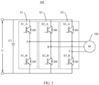
- FIG. 2 is a schematic diagram of a structure of the bridge arm circuit 105 according to this application.
- the switching bridge arm receives a bus voltage U by using a positive electrode and a negative electrode of a bus.
- the switching bridge arm is connected in parallel between the positive electrode and the negative electrode of the bus.
- the upper bridge arm switching transistor and the lower bridge arm switching transistor in each switching bridge arm are connected in series between the positive electrode and the negative electrode of the bus.
- the bridge arm circuit 105 includes a first switching bridge arm S1, a second switching bridge arm S2, and a third switching bridge arm S3. Two ends of the first switching bridge arm S1, the second switching bridge arm S2, and the third switching bridge arm S3 are respectively connected to the positive electrode and the negative electrode of the bus. Bridge arm midpoints of the first switching bridge arm S1, the second switching bridge arm S2, and the third switching bridge arm S3 are respectively connected to three-phase windings of the motor 106. Each of the bridge arm midpoints of the first switching bridge arm S1, the second switching bridge arm S2, and the third switching bridge arm S3 outputs a single-phase alternating current.
- the first switching bridge arm S1 includes a first upper bridge arm switching transistor S 1_A and a first lower bridge arm switching transistor S1_B.
- a drain of the first upper bridge arm switching transistor S1_A is electrically connected to one end of a capacitor C1 and one electrode of the bus
- a source of the first lower bridge arm switching transistor S1_B is electrically connected to the other end of the capacitor C1 and the other electrode of the bus
- a source of the first upper bridge arm switching transitor S1_A is electrically connected to a drain of the first lower bridge arm switching transistor S1_B and is used as a first bridge arm midpoint A of the first switching bridge arm S1.
- the first switching bridge arm S1 is configured to output a first-phase alternating current by using the first bridge arm midpoint A.
- the second switching bridge arm S2 includes a second upper bridge arm switching transistor S2_A and a second lower bridge arm switching transistor S2_B.
- a drain of the second upper bridge arm switching transistor S2_A is electrically connected to one end of the capacitor C1 and one electrode of the bus
- a source of the second lower bridge arm switching transistor S2_B is electrically connected to the other end of the capacitor C1 and the other electrode of the bus
- a source of the second upper bridge arm switching transistor S2_A is electrically connected to a drain of the second lower bridge arm switching transistor S2_B and is used as the second bridge arm midpoint B of the second switching bridge arm S2.
- the second bridge arm midpoint B is configured to output a second-phase alternating current.
- the third switching bridge arm S3 includes a third upper bridge arm switching transistor S3_A and a third lower bridge arm switching transistor S3_B.
- a drain of the third upper bridge arm switching transistor S3_A is electrically connected to one end of the capacitor C1 and one electrode of the bus
- a source of the third lower bridge arm switching transistor S3_B is electrically connected to the other end of the capacitor C1 and the other electrode of the bus
- a source of the third upper bridge arm S3_A is electrically connected to a drain of the third lower bridge arm switching transistor S3_B and is used as the third bridge arm midpoint C of the third switching bridge arm S3.
- the third bridge arm midpoint C is configured to output a third-phase alternating current.
- the upper bridge arm switching transistor and the lower bridge arm switching transistor in each switching bridge arm in the bridge arm circuit 105 are mutually turned on. For example, when the upper bridge arm switching transistor is turned on, the lower bridge arm switching transistor is turned off; and when the lower bridge arm switching transistor is turned on, the upper bridge arm switching transistor is turned off.
- the motor controller 100 further includes the capacitor C1.
- the capacitor C1 is electrically connected between the positive electrode and the negative electrode of the bus.
- the capacitor C1 is configured to stabilize the bus voltage.
- the upper bridge arm switching transistors and the lower bridge arm switching transistors of the first switching bridge arm S1, the second switching bridge arm S2, and the third switching bridge arm S3 are metal oxide semiconductor (MOS) transistors.
- MOS metal oxide semiconductor
- Each upper bridge arm switching transistor or lower bridge arm switching transistor includes a freewheeling diode D0.
- the freewheeling diode D0 is used as a freewheeling channel of a load current, and can prevent the switching transistor from being damaged.
- FIG. 3 is a circuit diagram of the backup power supply 102 according to this application.
- the backup power supply 102 includes a flyback conversion circuit.
- the flyback conversion circuit includes a power switching transistor M, a resistor R, a diode D2, a Zener diode DZ, a primary-side winding 1021, and a secondary-side winding 1022.
- a dotted terminal of the primary-side winding 1021 is connected to an anode of the Zener diode DZ, and the dotted terminal of the primary-side winding 1021 receives the bus voltage U.
- a cathode of the Zener diode DZ is connected to a cathode of the diode D2, and an anode of the diode D2 is connected to a drain of the power switching transistor M.
- a gate of the power switching transistor M receives a control signal of the control apparatus 104, a source of the power switching transistor M is connected to one end of the resistor R, and the other end of the resistor R is grounded.
- An output voltage Vo at two ends of the secondary-side winding 1022 supplies power to the safety state control circuit 103.
- the diode D2 and the Zener diode DZ that are connected in series are configured to provide overvoltage protection for the power switching transistor M.
- the diode D2 and the Zener diode DZ can prevent a peak voltage from breaking down the power switching transistor M.
- the primary-side winding 1021 When the power switching transistor M is turned on, the primary-side winding 1021 receives the bus voltage U and stores energy. When the power switching transistor M is turned off, the primary-side winding 1021 is coupled to the secondary-side winding 1022 to transmit the stored energy to the secondary-side winding 1022, so that the output voltage Vo of the secondary-side winding 1022 supplies power to the safety state control circuit 103.
- control apparatus 104 may output the control signal to control the power switching transistor M.
- control signal may be a PWM signal.
- the control apparatus 104 may adjust an output frequency of the PWM signal to adjust a switching frequency of the power switching transistor M, and the control apparatus 104 may further adjust a duty cycle of the PWM signal to adjust the output voltage Vo of the secondary-side winding 1022.
- a single-transistor flyback conversion circuit is used as an example of the flyback conversion circuit. Because the flyback conversion circuit includes the power switching transistor M, and the power switching transistor M has limited operating stability and a limited life in a high-voltage environment, when a received bus voltage U is high, reliability of the power switching transistor M is poor.
- the motor controller 100 provided in this application may control an operating status of the flyback conversion circuit based on an operating status of the main power supply and a value of the bus voltage. This improves reliability of the flyback conversion circuit in a high-voltage condition.
- the motor controller 100 further includes a power supply control circuit 107.
- the power supply control circuit 107 is configured to: in response to that the main power supply 101 operates normally, control an operating status of the flyback conversion circuit based on the bus voltage U.
- the power supply control circuit 107 may, in response to that the bus voltage U is greater than a first preset voltage, control the flyback conversion circuit in the backup power supply 102 to stop operating. It may be understood that in a condition in which the main power supply 101 operates normally and the bus voltage U is greater than the first preset voltage, the power supply control circuit 107 may control the flyback conversion circuit to stop operating. This reduces operating duration of the flyback conversion circuit in an environment in which the bus voltage U is excessively high, improves reliability of the flyback conversion circuit in the high-voltage condition, and reduces power consumption of the backup power supply 102.
- the power supply control circuit 107 may, in response to a result of comparing the bus voltage U to at least one of a plurality of voltage thresholds, control the operating status of the flyback conversion circuit.
- the plurality of voltage thresholds include a first voltage U1, a second voltage U2, and a third voltage U3.
- the power supply control circuit 107 may, in response to that the bus voltage U is less than or equal to the first voltage U1, control the flyback conversion circuit to stop operating.
- the power supply control circuit 107 may, in response to that the bus voltage U is greater than or equal to the second voltage U2 and less than or equal to the third voltage U3, control the flyback conversion circuit to operate normally.
- the first voltage U1 is less than or equal to the second voltage U2, the second voltage is less than or equal to the third voltage U3, and the third voltage U3 is less than or equal to a first preset voltage U4.
- the power supply control circuit 107 may, in response to that the bus voltage U is greater than the first voltage U1 and less than the second voltage U2 and in response to that the bus voltage U increases, control the flyback conversion circuit to stop operating.
- the power supply control circuit 107 may, in response to that the bus voltage U is greater than the first voltage U1 and less than the second voltage U2 and in response to that the bus voltage U decreases, control the flyback conversion circuit to operate normally.
- the power supply control circuit 107 may, in response to that the bus voltage U is greater than the third voltage U3 and less than the first preset voltage U4 and in response to that the bus voltage U increases, control the flyback conversion circuit to operate normally.
- the power supply control circuit 107 may, in response to that the bus voltage U is greater than the third voltage U3 and less than the first preset voltage U4 and in response to that the bus voltage U decreases, control the flyback conversion circuit to stop operating.
- the power supply control circuit 107 may, in response to that the bus voltage U is greater than the second voltage U2, control the flyback conversion circuit to operate normally, and control the flyback conversion circuit to stop operating after preset time T.
- the power supply control circuit 107 may directly control the flyback conversion circuit to stop operating.
- that the main power supply 101 operates normally means that an output voltage Vo1 of the main power supply 101 is greater than or equal to a second preset voltage.
- That the flyback conversion circuit operates normally may include that the output voltage of the secondary-side winding 1022 is not zero, the switching frequency of the power switching transistor M is not zero, and the like.
- That the flyback conversion circuit stops operating may include that the switching frequency of the power switching transistor M is zero, a side that is of the primary-side winding 1021 and that is configured to receive the bus voltage U is disconnected, the output voltage of the secondary-side winding 1022 is zero, and the like.
- the power supply control circuit 107 is further configured to: in response to that the main power supply 101 operates abnormally, control the flyback conversion circuit to operate normally. That the main power supply 101 operates abnormally means that the output voltage Vo1 of the main power supply is less than the second preset voltage.
- the first preset voltage U4 may be 750 V
- the first voltage U1 may be 60 V
- the second voltage U2 may be 190 V
- the third voltage U3 may be 600 V
- the power supply control circuit 107 controls the operating status of the flyback conversion circuit based on different bus voltages U, to optimize control logic of the flyback conversion circuit, and to maximumly control the flyback conversion circuit to stop operating in the high-voltage condition. This improves the reliability of the flyback conversion circuit in the high-voltage condition, and prolongs a service life of the flyback conversion circuit.
- the power supply control circuit 107 may further control the flyback conversion circuit to operate normally, so that the flyback conversion circuit can quickly start when the main power supply 101 operates abnormally. This ensures continuous power supply to the safety state control circuit 103, and improves safety performance of the motor 106.
- the power supply control circuit 107 may obtain the bus voltage by using an electronic component such as a voltage sensor, a voltage detection circuit, or the like, to obtain the result of comparing the bus voltage with the plurality of voltage thresholds, or directly obtain the result of comparing the bus voltage with the plurality of voltage thresholds, to perform corresponding control.
- an electronic component such as a voltage sensor, a voltage detection circuit, or the like
- the bus voltage U is controlled by the motor controller 100 and a vehicle control unit (VCU) and dynamically changes.
- VCU vehicle control unit
- the motor controller 100 starts to be powered on, and the bus voltage U gradually increases from zero.
- the bus voltage U is less than or equal to the first voltage U1
- the power supply control circuit 107 controls the flyback conversion circuit to stop operating, and an output voltage of the flyback conversion circuit is zero.
- the motor 106 continues to run, and the bus voltage U continues to increase.
- the bus voltage U increases to be greater than or equal to the second voltage U2
- a power-on procedure of the motor controller 100 ends, and the motor controller 100 enters a running state.
- the power supply control circuit 107 controls the flyback conversion circuit to operate normally, and the output voltage of the flyback conversion circuit is not zero.
- the motor 106 continues to run, and the bus voltage U continues to increase.
- the bus voltage U increases to be greater than the first preset voltage U4
- the bus voltage U is high, and the power supply control circuit 107 controls the flyback conversion circuit to stop operating. This ensures reliability of the flyback conversion circuit in a high-voltage environment.
- the motor 106 continues to run, and in this case, the bus voltage U decreases.
- the bus voltage U decreases to be less than or equal to the third voltage U3
- the bus voltage U is already out of the high-voltage condition, and the power supply control circuit 107 controls the flyback conversion circuit to operate normally.
- the motor 106 gradually stops operating, the motor controller 100 enters from the running state to a power-off procedure, and the bus voltage U continues to decrease.
- the power supply control circuit 107 controls the flyback conversion circuit to suspend or stop operating.
- the motor controller 100 and the VCU control the bus voltage U based on a running status of the motor 106. As the running status of the motor 106 is switched, the bus voltage U also changes accordingly.
- the motor controller 100 provided in this application may control the operating status of the flyback conversion circuit based on a dynamic change of the bus voltage U in a case in which the main power supply 101 operates normally. This improves reliability of the power switching transistor M in the flyback conversion circuit in the high-voltage condition, and prolongs a service life of the power switching transistor M.
- a running status and a running time sequence of the motor 106 are the same as the running status and the running time sequence in FIG. 4 , but a control policy of the power supply control circuit 107 for the flyback conversion circuit is different.
- the motor controller 100 is in a power-on procedure.
- the power supply control circuit 107 controls the flyback conversion circuit to operate normally.
- the flyback conversion circuit starts a self-check procedure to check whether the flyback conversion circuit can operate normally, to reduce a risk that when the main power supply 101 operates abnormally, the flyback conversion circuit cannot operate normally and causes the safety state control circuit 103 to be powered off.
- the flyback conversion circuit completes the self-check procedure.
- the power supply control circuit 107 controls the flyback conversion circuit to stop operating. This reduces operating duration of the flyback conversion circuit, and reduces power consumption of the flyback conversion circuit.
- a running status and a running time sequence of the motor 106 are the same as the running status and the running time sequence in FIG. 4 , but a control policy of the power supply control circuit 107 for the flyback conversion circuit is different.
- the power supply control circuit 107 controls the flyback conversion circuit to continuously stop operating or stop operating. This can further reduce the power consumption of the flyback conversion circuit, reduce the operating duration of the flyback conversion circuit in the high-voltage condition, and improve the reliability of the power switching transistor M.
- FIG. 7 is a time sequence diagram of the output voltage of the backup power supply 102, the output voltage of the main power supply 101, and an input voltage of the safety state control circuit 103 in the motor controller 100 according to this application.
- a broken line L1 represents the output voltage of the backup power supply 102
- a broken line L2 represents the output voltage of the main power supply 101
- a broken line L3 represents the input voltage of the safety state control circuit 103.
- the flyback conversion circuit is in a normal operating state.
- the output voltage of the main power supply 101 is U6, the main power supply 101 operates normally, and the input voltage of the safety state control circuit 103 is determined by the output voltage U6 of the main power supply 101. Therefore, the broken line L2 and the broken line L3 overlap before the moment T1.
- the main power supply 101 encounters an abnormal power failure, and enters an abnormal operating state. In this case, the output voltage of the main power supply 101 decreases, and an output voltage U5 of the backup power supply 102 remains constant.
- the input voltage of the safety state control circuit 103 is determined by the output voltage U5 of the backup power supply 102. Because the backup power supply 102 continuously operates normally, the backup power supply 102 can continue to supply power to the safety state control circuit 103 when the main power supply 101 operates abnormally.
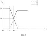
- FIG. 8 is another time sequence diagram of the output voltage of the backup power supply 102, the output voltage of the main power supply 101, and the input voltage of the safety state control circuit 103 in the motor controller 100 according to this application.
- a broken line L1 represents the output voltage of the backup power supply 102
- a broken line L2 represents the output voltage of the main power supply 101
- a broken line L3 represents the input voltage of the safety state control circuit 103.
- an example in which the flyback conversion circuit stops operating is used.
- an output voltage U6 of the main power supply 101 is not zero, the main power supply 101 operates normally, and the input voltage of the safety state control circuit 103 is determined by the output voltage U6 of the main power supply 101. Therefore, the broken line L2 and the broken line L3 overlap before the moment T1.
- the main power supply 101 encounters an abnormal power failure, and enters an abnormal operating state. In this case, the output voltage of the main power supply 101 decreases.
- the power supply control circuit 107 in response to that the main power supply 101 operates abnormally, controls the flyback conversion circuit to operate normally, and the output voltage of the backup power supply 102 gradually increases from zero.
- the output voltage of the backup power supply 102 increases to U8, and the output voltage of the main power supply 101 decreases to U8.
- the output voltage of the backup power supply 102 increases to a current value of the output voltage of the main power supply 101, and the input voltage of the safety state control circuit 103 is determined by the output voltage U8 of the backup power supply 102.
- the output voltage of the backup power supply 102 continues to increase, and finally remains constant. This can ensure that a power supply voltage of the safety state control circuit 103 is stable. Therefore, after the moment T2, the broken line L1 and the broken line L3 overlap.
- the powertrain provided in this application includes the motor controller 100 and the motor 106.
- the motor controller 100 is configured to: in response to that the main power supply 101 operates normally, control the operating status of the flyback conversion circuit based on the bus voltage U; or control, when the main power supply 101 operates abnormally, the flyback conversion circuit to operate normally.
- the motor controller 100 in the powertrain provided in this application may control the operating status of the flyback conversion circuit based on the operating status of the main power supply 101 and the value of the bus voltage. This improves the reliability of the flyback conversion circuit in the high-voltage condition.
Landscapes
- Engineering & Computer Science (AREA)
- Power Engineering (AREA)
- Inverter Devices (AREA)
- Stopping Of Electric Motors (AREA)
- Control Of Direct Current Motors (AREA)
Abstract
This application provides a motor controller. The motor controller includes a power supply control circuit, a safety state control circuit, and switching bridge aims. The power supply control circuit is configured to control a backup power supply to supply power to the safety state control circuit. The backup power supply includes a flyback conversion circuit. The power supply control circuit is configured to: in response to that a main power supply operates normally and a bus voltage is greater than a first preset voltage, control the flyback conversion circuit to stop operating. This application further provides a powertrain. Therefore, the motor controller and the powertrain provided in this application can improve reliability of the flyback conversion circuit.
Description
- This application relates to the field of motor control technologies, and in particular, to a motor controller and a powertrain.
- With development of a motor control technology, a safety state control circuit has been used more widely. A power supply architecture of the safety state control circuit generally includes a main power supply and a backup power supply. The safety state control circuit receives electric energy output by the main power supply and the backup power supply, and controls a motor to enter a safety state. However, the backup power supply generally includes a flyback conversion circuit, and a power switching transistor in the flyback conversion circuit has poor reliability when an input voltage is high.
- In view of the foregoing problem, this application provides a motor controller and a powertrain, to control an operating status of a flyback conversion circuit based on an operating status of a main power supply and a voltage value of a bus voltage. This improves reliability of the flyback conversion circuit in a high-voltage condition.
- According to a first aspect, this application provides a motor controller, where the motor controller includes a power supply control circuit, a safety state control circuit, and switching bridge arms. The safety state control circuit is configured to: receive electric energy of a main power supply or a backup power supply and control the switching bridge arm. The power supply control circuit is configured to control the backup power supply to supply power to the safety state control circuit. The backup power supply includes a flyback conversion circuit. The flyback conversion circuit is configured to: receive bus voltages at two ends of the switching bridge arm, convert the bus voltages, and supply power to the safety state control circuit. The power supply control circuit is configured to: in response to that the main power supply operates normally and the bus voltage is greater than a first preset voltage, control the flyback conversion circuit to stop operating. The motor controller provided in this application may control an operating status of the flyback conversion circuit in the backup power supply based on the bus voltage when the main power supply operates normally. This improves reliability of the flyback conversion circuit when the bus voltage is high, and prolongs a service life of a power switching transistor in the flyback conversion circuit.
- With reference to the first aspect, in a possible implementation, in response to that the main power supply operates normally, the power supply control circuit is configured to: in response to a result of comparing the bus voltage with at least one of a plurality of voltage thresholds, control an operating status of the flyback conversion circuit. The motor controller provided in this application may control the operating status of the flyback conversion circuit in the backup power supply based on the result of comparing the bus voltage with the plurality of voltage thresholds when the main power supply operates normally. This improves the reliability of the flyback conversion circuit when the bus voltage is high, and prolongs the service life of the power switching transistor in the flyback conversion circuit.
- With reference to the first aspect, in a possible implementation, the plurality of voltage thresholds include a first voltage, a second voltage, and a third voltage, and in response to that the main power supply operates normally, the power supply control circuit is configured to: in response to that the bus voltage is less than or equal to the first voltage, control the flyback conversion circuit to stop operating; and in response to that the bus voltage is greater than or equal to the second voltage and less than or equal to the third voltage, control the flyback conversion circuit to operate normally. The first voltage is less than or equal to the second voltage, the second voltage is less than or equal to the third voltage, and the third voltage is less than or equal to the first preset voltage. When the main power supply operates normally, the motor controller provided in this application may, in response to that the bus voltage is less than or equal to the first voltage, control the flyback conversion circuit to stop operating, and in response to that the bus voltage is greater than or equal to the second voltage and less than or equal to the third voltage, control the flyback conversion circuit to operate normally. In this way, the motor controller provided in this application may dynamically adjust the operating status of the flyback conversion circuit. This reduces power consumption of the flyback conversion circuit and a damage risk in a high-voltage environment.
- With reference to the first aspect, in a possible implementation, in response to that the main power supply operates normally, the power supply control circuit is configured to: in response to that the bus voltage is greater than the first voltage and less than the second voltage and in response to that the bus voltage increases, control the flyback conversion circuit to stop operating; and in response to that the bus voltage is greater than the first voltage and less than the second voltage and in response to that the bus voltage decreases, control the flyback conversion circuit to operate normally.
- With reference to the first aspect, in a possible implementation, in response to that the main power supply operates normally, the power supply control circuit is configured to: in response to that the bus voltage is greater than the third voltage and less than the first preset voltage and in response to that the bus voltage increases, control the flyback conversion circuit to operate normally; and in response to that the bus voltage is greater than the third voltage and less than the first preset voltage and in response to that the bus voltage decreases, control the flyback conversion circuit to stop operating.
- With reference to the first aspect, in a possible implementation, the plurality of voltage thresholds include the second voltage, and in response to that the main power supply operates normally, the power supply control circuit is configured to: in response to that the bus voltage is greater than the second voltage, control the flyback conversion circuit to operate normally, and control the flyback conversion circuit to stop operating after preset time. The motor controller provided in this application may control the flyback conversion circuit to start a self-check procedure when the main power supply operates normally, and control the flyback conversion circuit to stop operating when the self-check procedure is completed after the preset time. This can reduce a risk that the flyback conversion circuit cannot start normally when the main power supply enters an abnormal operating state.
- With reference to the first aspect, in a possible implementation, in response to that the main power supply operates normally, the power supply control circuit is configured to: control the flyback conversion circuit to stop operating. The motor controller provided in this application may control the flyback conversion circuit to continuously stop operating when the main power supply operates normally. This can reduce the power consumption of the flyback conversion circuit, and improve the reliability of the flyback conversion circuit in the high-voltage environment.
- With reference to the first aspect, in a possible implementation, the power supply control circuit is configured to: in response to that the main power supply operates abnormally, control the flyback conversion circuit to operate normally. That the main power supply operates abnormally means that an output voltage of the main power supply is less than a second preset voltage.
- With reference to the first aspect, in a possible implementation, the flyback conversion circuit includes a power switching transistor, that the main power supply operates normally means that the output voltage of the main power supply is greater than or equal to the second preset voltage, that the flyback conversion circuit stops operating means that a switching frequency of the power switching transistor is zero and the power switching transistor is in an off state, and that the flyback conversion circuit operates normally means that the switching frequency of the power switching transistor is not zero.
- With reference to the first aspect, in a possible implementation, the motor controller includes a control apparatus, each switching bridge arm includes an upper bridge arm switching transistor and a lower bridge arm switching transistor, the safety state control circuit is configured to output a safety state control signal to control the control apparatus, and the control apparatus is configured to: control, based on the safety state control signal, each upper bridge arm switching transistor and each lower bridge arm switching transistor of the switching bridge arm to be turned off; control, based on the safety state control signal, each upper bridge arm switching transistor of the switching bridge arm to be turned off and each lower bridge arm switching transistor to be turned on; or control, based on the safety state control signal, each upper bridge arm switching transistor of the switching bridge arm to be turned on and each lower bridge arm switching transistor to be turned off.
- According to a second aspect, this application provides a powertrain, including a motor and the motor controller provided in any one of the implementations of the first aspect, where the motor controller is configured to control running of the motor.
- In addition, for beneficial effects corresponding to implementations of the second aspect, refer to beneficial effects obtained in the implementations corresponding to the first aspect. Details are not described herein again.
-
-
FIG. 1 is a schematic diagram of a structure of a motor controller according to this application; -
FIG. 2 is a schematic diagram of a structure of a bridge arm circuit according to this application; -
FIG. 3 is a circuit diagram of a backup power supply according to this application; -
FIG. 4 is a time sequence diagram of an operating procedure of a motor controller according to this application; -
FIG. 5 is a time sequence diagram of another operating procedure of a motor controller according to this application; -
FIG. 6 is a time sequence diagram of still another operating procedure of a motor controller according to this application; -
FIG. 7 is a time sequence diagram of an output voltage of a backup power supply, an output voltage of a main power supply, and an input voltage of a safety state control circuit according to this application; and -
FIG. 8 is another time sequence diagram of an output voltage of a backup power supply, an output voltage of a main power supply, and an input voltage of a safety state control circuit according to this application. - Description of reference signs of main components:
-
Motor controller 100 -
Main power supply 101 -
Backup power supply 102 - High-
voltage battery 102a - Low-
voltage battery 101a - Safety
state control circuit 103 -
Control apparatus 104 -
Bridge arm circuit 105 -
Motor 106 - Diodes D1 and D2
- Bus voltage U
- Capacitor C1
- Primary-
side winding 1021 - Secondary-
side winding 1022 - Zener diode DZ
- Leakage inductance L
- Power switching transistor M
- Resistor R
- The following clearly describes technical solutions in embodiments of this application with reference to accompanying drawings in embodiments of this application.
- It may be understood that a connection relationship described in this application is a direct or indirect connection. For example, that A is connected to B may be that A is directly connected to B, or may be that A is indirectly connected to B by using one or more other electrical components. For example, A may be directly connected to C, and C may be directly connected to B, so that A and B are connected by using C. It may be further understood that "A is connected to B" described in this application may be that A is directly connected to B, or may be that A is indirectly connected to B by using one or more other electrical components.
- In descriptions of this application, unless otherwise specified, "/" means "or". For example, A/B may represent A or B. The term "and/or" in this specification describes only an association relationship between associated objects and indicates that three relationships may exist. For example, A and/or B may represent the following three cases: Only A exists, both A and B exist, and only B exists.
- In descriptions of this application, the words such as "first", "second", and the like are merely used to distinguish between different objects, and do not limit quantities and execution sequences. In addition, the words such as "first", "second", and the like are not necessarily different. In addition, the terms "including" and "having" and any other variants thereof are intended to cover a non-exclusive inclusion.
- The technical solutions of this application are further described below in detail with reference to the accompanying drawings.
-
FIG. 1 is a schematic diagram of a structure of amotor controller 100 according to this application. Themotor controller 100 is configured to control running of amotor 106. Themotor controller 100 includes amain power supply 101, abackup power supply 102, a safetystate control circuit 103, acontrol apparatus 104, and abridge arm circuit 105. - The
main power supply 101 and thebackup power supply 102 jointly supply power to the safetystate control circuit 103. Specifically, an output terminal of themain power supply 101 is connected to an input terminal of the safetystate control circuit 103 by using a diode D1, and an output terminal of thebackup power supply 102 is connected to an input terminal of the safetystate control circuit 103 by using another diode D1. In this way, when amplitudes of the output voltages of themain power supply 101 and thebackup power supply 102 are different, a power supply voltage of the safetystate control circuit 103 is a larger output voltage of themain power supply 101 and thebackup power supply 102. For example, if an output voltage of themain power supply 101 is a direct current 12 V, and an output voltage of thebackup power supply 102 is a direct current 10 V, the power supply voltage of the safetystate control circuit 103 is 12 V - In an embodiment, a low-
voltage battery 101a supplies power to themain power supply 101, and a high-voltage battery 102a supplies power to thebackup power supply 102. An output terminal of the high-voltage battery 102a is connected to an end of each upper bridge arm switching transistor. In this way, an output voltage of the high-voltage battery 102a is a bus voltage, and an input voltage of thebackup power supply 102 is also a bus voltage, so that thebackup power supply 102 may convert the input bus voltage, and supply power to the safetystate control circuit 103. - The safety
state control circuit 103 is configured to control themotor 106 to enter a safety state. Specifically, based on a functional safety requirement of themotor 106, to prevent themotor 106 from generating unexpected torque, the safetystate control circuit 103 may control themotor 106 to enter the safety state in an emergency. The emergency includes a fault in themotor controller 100, a fault in themotor 106, and the like. The safetystate control circuit 103 may output a safety state control signal to thecontrol apparatus 104, and thecontrol apparatus 104 may control, based on the safety state control signal, thebridge arm circuit 105 to control themotor 106 to enter the safety state. Thebridge arm circuit 105 includes switching bridge arms. Each switching bridge arm includes an upper bridge arm switching transistor and a lower bridge arm switching transistor. A connection point between the upper bridge arm switching transistor and the lower bridge arm switching transistor in each switching bridge arm is a bridge arm midpoint of the switching bridge arm, and each switching bridge arm outputs a corresponding single-phase alternating current to themotor 106 by using the bridge arm midpoint. - The
control apparatus 104 may control the upper bridge arm switching transistor and the lower bridge arm switching transistor in thebridge arm circuit 105 to be turned on or off, to control themotor 106 to enter the safety state. For example, the safety state control signal includes a stop pulse-width modulation output (SPO) signal and an active short circuit (ASC) signal. Thecontrol apparatus 104 may control, based on the SPO signal, each upper bridge arm switching transistor and each lower bridge arm switching transistor in thebridge arm circuit 105 to be turned off, so that themotor 106 enters an SPO safety state; may control, based on the ASC signal, each upper bridge arm switching transistor in thebridge arm circuit 105 to be turned off and each lower bridge arm switching transistor to be turned on, so that themotor 106 enters an ASC safety state; or may control, based on an ASC signal, each upper bridge arm switching transistor in thebridge arm circuit 105 to be turned on and each lower bridge arm switching transistor to be turned off, so that themotor 106 enters an ASC safety state. - It may be understood that the
control apparatus 104 outputs a control signal to control the upper bridge arm switching transistor and the lower bridge arm switching transistor. A pulse-width modulation (PWM) signal is used as an example. Thecontrol apparatus 104 may adjust an output frequency of the PWM signal to adjust switching frequencies of the upper bridge arm switching transistor and the lower bridge arm switching transistor, and thecontrol apparatus 104 may further adjust a duty cycle of the PWM signal to adjust a three-phase current output by thebridge arm circuit 105. - In this embodiment of this application, the
control apparatus 104 may include a pulse-width modulation (PWM) controller, a central processing unit (CPU), another general purpose processor, a digital signal processor (DSP), an application-specific integrated circuit (ASIC), a field-programmable gate array (FPGA), or another programmable logic device, a discrete gate, a transistor logic device, or the like. - In an embodiment, an anode of the diode D1 may alternatively be connected to one end of a filter capacitor, the other end of the filter capacitor is grounded, and the filter capacitor is configured to filter the output voltage of the
main power supply 101 and/or the output voltage of thebackup power supply 102. -
FIG. 2 is a schematic diagram of a structure of thebridge arm circuit 105 according to this application. As shown inFIG. 2 , the switching bridge arm receives a bus voltage U by using a positive electrode and a negative electrode of a bus. The switching bridge arm is connected in parallel between the positive electrode and the negative electrode of the bus. The upper bridge arm switching transistor and the lower bridge arm switching transistor in each switching bridge arm are connected in series between the positive electrode and the negative electrode of the bus. - For example, the
bridge arm circuit 105 includes a first switching bridge arm S1, a second switching bridge arm S2, and a third switching bridge arm S3. Two ends of the first switching bridge arm S1, the second switching bridge arm S2, and the third switching bridge arm S3 are respectively connected to the positive electrode and the negative electrode of the bus. Bridge arm midpoints of the first switching bridge arm S1, the second switching bridge arm S2, and the third switching bridge arm S3 are respectively connected to three-phase windings of themotor 106. Each of the bridge arm midpoints of the first switching bridge arm S1, the second switching bridge arm S2, and the third switching bridge arm S3 outputs a single-phase alternating current. - The first switching bridge arm S1 includes a first upper bridge arm switching transistor S 1_A and a first lower bridge arm switching transistor S1_B. A drain of the first upper bridge arm switching transistor S1_A is electrically connected to one end of a capacitor C1 and one electrode of the bus, a source of the first lower bridge arm switching transistor S1_B is electrically connected to the other end of the capacitor C1 and the other electrode of the bus, and a source of the first upper bridge arm switching transitor S1_A is electrically connected to a drain of the first lower bridge arm switching transistor S1_B and is used as a first bridge arm midpoint A of the first switching bridge arm S1. The first switching bridge arm S1 is configured to output a first-phase alternating current by using the first bridge arm midpoint A.
- The second switching bridge arm S2 includes a second upper bridge arm switching transistor S2_A and a second lower bridge arm switching transistor S2_B. A drain of the second upper bridge arm switching transistor S2_A is electrically connected to one end of the capacitor C1 and one electrode of the bus, a source of the second lower bridge arm switching transistor S2_B is electrically connected to the other end of the capacitor C1 and the other electrode of the bus, and a source of the second upper bridge arm switching transistor S2_A is electrically connected to a drain of the second lower bridge arm switching transistor S2_B and is used as the second bridge arm midpoint B of the second switching bridge arm S2. The second bridge arm midpoint B is configured to output a second-phase alternating current.
- The third switching bridge arm S3 includes a third upper bridge arm switching transistor S3_A and a third lower bridge arm switching transistor S3_B. A drain of the third upper bridge arm switching transistor S3_A is electrically connected to one end of the capacitor C1 and one electrode of the bus, a source of the third lower bridge arm switching transistor S3_B is electrically connected to the other end of the capacitor C1 and the other electrode of the bus, and a source of the third upper bridge arm S3_A is electrically connected to a drain of the third lower bridge arm switching transistor S3_B and is used as the third bridge arm midpoint C of the third switching bridge arm S3. The third bridge arm midpoint C is configured to output a third-phase alternating current.
- It may be understood that when the
motor 106 does not enter the safety state, the upper bridge arm switching transistor and the lower bridge arm switching transistor in each switching bridge arm in thebridge arm circuit 105 are mutually turned on. For example, when the upper bridge arm switching transistor is turned on, the lower bridge arm switching transistor is turned off; and when the lower bridge arm switching transistor is turned on, the upper bridge arm switching transistor is turned off. - In an embodiment, the
motor controller 100 further includes the capacitor C1. The capacitor C1 is electrically connected between the positive electrode and the negative electrode of the bus. The capacitor C1 is configured to stabilize the bus voltage. - In an embodiment, the upper bridge arm switching transistors and the lower bridge arm switching transistors of the first switching bridge arm S1, the second switching bridge arm S2, and the third switching bridge arm S3 are metal oxide semiconductor (MOS) transistors. Each upper bridge arm switching transistor or lower bridge arm switching transistor includes a freewheeling diode D0. The freewheeling diode D0 is used as a freewheeling channel of a load current, and can prevent the switching transistor from being damaged.
-
FIG. 3 is a circuit diagram of thebackup power supply 102 according to this application. Thebackup power supply 102 includes a flyback conversion circuit. The flyback conversion circuit includes a power switching transistor M, a resistor R, a diode D2, a Zener diode DZ, a primary-side winding 1021, and a secondary-side winding 1022. - A dotted terminal of the primary-side winding 1021 is connected to an anode of the Zener diode DZ, and the dotted terminal of the primary-side winding 1021 receives the bus voltage U. A cathode of the Zener diode DZ is connected to a cathode of the diode D2, and an anode of the diode D2 is connected to a drain of the power switching transistor M. A gate of the power switching transistor M receives a control signal of the
control apparatus 104, a source of the power switching transistor M is connected to one end of the resistor R, and the other end of the resistor R is grounded. An output voltage Vo at two ends of the secondary-side winding 1022 supplies power to the safetystate control circuit 103. - The diode D2 and the Zener diode DZ that are connected in series are configured to provide overvoltage protection for the power switching transistor M. For example, the diode D2 and the Zener diode DZ can prevent a peak voltage from breaking down the power switching transistor M.
- When the power switching transistor M is turned on, the primary-side winding 1021 receives the bus voltage U and stores energy. When the power switching transistor M is turned off, the primary-side winding 1021 is coupled to the secondary-side winding 1022 to transmit the stored energy to the secondary-side winding 1022, so that the output voltage Vo of the secondary-side winding 1022 supplies power to the safety
state control circuit 103. - It may be understood that the
control apparatus 104 may output the control signal to control the power switching transistor M. In an embodiment, the control signal may be a PWM signal. Thecontrol apparatus 104 may adjust an output frequency of the PWM signal to adjust a switching frequency of the power switching transistor M, and thecontrol apparatus 104 may further adjust a duty cycle of the PWM signal to adjust the output voltage Vo of the secondary-side winding 1022. - It may be understood that because the primary-side winding 1021 is not completely coupled to the secondary-side winding 1022, an equivalent leakage inductance L is generated, and the leakage inductance L is equivalently electrically connected between an undotted terminal of the primary-side winding 1021 and the anode of the diode D2.
- It may be understood that in this embodiment, a single-transistor flyback conversion circuit is used as an example of the flyback conversion circuit. Because the flyback conversion circuit includes the power switching transistor M, and the power switching transistor M has limited operating stability and a limited life in a high-voltage environment, when a received bus voltage U is high, reliability of the power switching transistor M is poor.
- Therefore, the
motor controller 100 provided in this application may control an operating status of the flyback conversion circuit based on an operating status of the main power supply and a value of the bus voltage. This improves reliability of the flyback conversion circuit in a high-voltage condition. - Specifically, refer to
FIG. 1 to FIG. 3 . Themotor controller 100 further includes a powersupply control circuit 107. The powersupply control circuit 107 is configured to: in response to that themain power supply 101 operates normally, control an operating status of the flyback conversion circuit based on the bus voltage U. - For example, the power
supply control circuit 107 may, in response to that the bus voltage U is greater than a first preset voltage, control the flyback conversion circuit in thebackup power supply 102 to stop operating. It may be understood that in a condition in which themain power supply 101 operates normally and the bus voltage U is greater than the first preset voltage, the powersupply control circuit 107 may control the flyback conversion circuit to stop operating. This reduces operating duration of the flyback conversion circuit in an environment in which the bus voltage U is excessively high, improves reliability of the flyback conversion circuit in the high-voltage condition, and reduces power consumption of thebackup power supply 102. - For another example, the power
supply control circuit 107 may, in response to a result of comparing the bus voltage U to at least one of a plurality of voltage thresholds, control the operating status of the flyback conversion circuit. For example, the plurality of voltage thresholds include a first voltage U1, a second voltage U2, and a third voltage U3. The powersupply control circuit 107 may, in response to that the bus voltage U is less than or equal to the first voltage U1, control the flyback conversion circuit to stop operating. For another example, the powersupply control circuit 107 may, in response to that the bus voltage U is greater than or equal to the second voltage U2 and less than or equal to the third voltage U3, control the flyback conversion circuit to operate normally. The first voltage U1 is less than or equal to the second voltage U2, the second voltage is less than or equal to the third voltage U3, and the third voltage U3 is less than or equal to a first preset voltage U4. - For still another example, the power
supply control circuit 107 may, in response to that the bus voltage U is greater than the first voltage U1 and less than the second voltage U2 and in response to that the bus voltage U increases, control the flyback conversion circuit to stop operating. Alternatively, the powersupply control circuit 107 may, in response to that the bus voltage U is greater than the first voltage U1 and less than the second voltage U2 and in response to that the bus voltage U decreases, control the flyback conversion circuit to operate normally. - For yet another example, the power
supply control circuit 107 may, in response to that the bus voltage U is greater than the third voltage U3 and less than the first preset voltage U4 and in response to that the bus voltage U increases, control the flyback conversion circuit to operate normally. Alternatively, the powersupply control circuit 107 may, in response to that the bus voltage U is greater than the third voltage U3 and less than the first preset voltage U4 and in response to that the bus voltage U decreases, control the flyback conversion circuit to stop operating. - For still yet another example, in response to that the
main power supply 101 operates normally, the powersupply control circuit 107 may, in response to that the bus voltage U is greater than the second voltage U2, control the flyback conversion circuit to operate normally, and control the flyback conversion circuit to stop operating after preset time T. Alternatively, the powersupply control circuit 107 may directly control the flyback conversion circuit to stop operating. - In an embodiment, that the
main power supply 101 operates normally means that an output voltage Vo1 of themain power supply 101 is greater than or equal to a second preset voltage. That the flyback conversion circuit operates normally may include that the output voltage of the secondary-side winding 1022 is not zero, the switching frequency of the power switching transistor M is not zero, and the like. That the flyback conversion circuit stops operating may include that the switching frequency of the power switching transistor M is zero, a side that is of the primary-side winding 1021 and that is configured to receive the bus voltage U is disconnected, the output voltage of the secondary-side winding 1022 is zero, and the like. - In addition, the power
supply control circuit 107 is further configured to: in response to that themain power supply 101 operates abnormally, control the flyback conversion circuit to operate normally. That themain power supply 101 operates abnormally means that the output voltage Vo1 of the main power supply is less than the second preset voltage. - In this embodiment, the first preset voltage U4 may be 750 V, the first voltage U1 may be 60 V, the second voltage U2 may be 190 V, and the third voltage U3 may be 600 V
- It may be understood that when the
main power supply 101 operates normally, the powersupply control circuit 107 controls the operating status of the flyback conversion circuit based on different bus voltages U, to optimize control logic of the flyback conversion circuit, and to maximumly control the flyback conversion circuit to stop operating in the high-voltage condition. This improves the reliability of the flyback conversion circuit in the high-voltage condition, and prolongs a service life of the flyback conversion circuit. In addition, when themain power supply 101 operates abnormally, the powersupply control circuit 107 may further control the flyback conversion circuit to operate normally, so that the flyback conversion circuit can quickly start when themain power supply 101 operates abnormally. This ensures continuous power supply to the safetystate control circuit 103, and improves safety performance of themotor 106. - In an embodiment, the power
supply control circuit 107 may obtain the bus voltage by using an electronic component such as a voltage sensor, a voltage detection circuit, or the like, to obtain the result of comparing the bus voltage with the plurality of voltage thresholds, or directly obtain the result of comparing the bus voltage with the plurality of voltage thresholds, to perform corresponding control. - The following describes operating procedures of the
motor controller 100 with reference toFIG. 4 and FIG. 5 . - As shown in
FIG. 4 , in this embodiment, an example in which themain power supply 101 operates normally is used. As themotor 106 runs, the bus voltage U is controlled by themotor controller 100 and a vehicle control unit (VCU) and dynamically changes. - At a moment T0, the
motor controller 100 starts to be powered on, and the bus voltage U gradually increases from zero. In this case, the bus voltage U is less than or equal to the first voltage U1, the powersupply control circuit 107 controls the flyback conversion circuit to stop operating, and an output voltage of the flyback conversion circuit is zero. - At a moment T1, the
motor 106 continues to run, and the bus voltage U continues to increase. When the bus voltage U increases to be greater than or equal to the second voltage U2, a power-on procedure of themotor controller 100 ends, and themotor controller 100 enters a running state. In this case, the powersupply control circuit 107 controls the flyback conversion circuit to operate normally, and the output voltage of the flyback conversion circuit is not zero. - At a moment T2, the
motor 106 continues to run, and the bus voltage U continues to increase. When the bus voltage U increases to be greater than the first preset voltage U4, the bus voltage U is high, and the powersupply control circuit 107 controls the flyback conversion circuit to stop operating. This ensures reliability of the flyback conversion circuit in a high-voltage environment. - At a moment T3, the
motor 106 continues to run, and in this case, the bus voltage U decreases. When the bus voltage U decreases to be less than or equal to the third voltage U3, the bus voltage U is already out of the high-voltage condition, and the powersupply control circuit 107 controls the flyback conversion circuit to operate normally. - At a moment T4, the
motor 106 gradually stops operating, themotor controller 100 enters from the running state to a power-off procedure, and the bus voltage U continues to decrease. When the bus voltage U decreases to be less than or equal to the first voltage U1, the powersupply control circuit 107 controls the flyback conversion circuit to suspend or stop operating. - It may be understood that in an embodiment, the
motor controller 100 and the VCU control the bus voltage U based on a running status of themotor 106. As the running status of themotor 106 is switched, the bus voltage U also changes accordingly. Themotor controller 100 provided in this application may control the operating status of the flyback conversion circuit based on a dynamic change of the bus voltage U in a case in which themain power supply 101 operates normally. This improves reliability of the power switching transistor M in the flyback conversion circuit in the high-voltage condition, and prolongs a service life of the power switching transistor M. - As shown in
FIG. 5 , in another embodiment, a running status and a running time sequence of themotor 106 are the same as the running status and the running time sequence inFIG. 4 , but a control policy of the powersupply control circuit 107 for the flyback conversion circuit is different. - Specifically, at a moment T1, the
motor controller 100 is in a power-on procedure. When the bus voltage U increases to be greater than or equal to the second voltage U2, the powersupply control circuit 107 controls the flyback conversion circuit to operate normally. In this case, the flyback conversion circuit starts a self-check procedure to check whether the flyback conversion circuit can operate normally, to reduce a risk that when themain power supply 101 operates abnormally, the flyback conversion circuit cannot operate normally and causes the safetystate control circuit 103 to be powered off. - At a moment T2, the flyback conversion circuit completes the self-check procedure. After preset time, the power
supply control circuit 107 controls the flyback conversion circuit to stop operating. This reduces operating duration of the flyback conversion circuit, and reduces power consumption of the flyback conversion circuit. - As shown in
FIG. 6 , in still another embodiment, a running status and a running time sequence of themotor 106 are the same as the running status and the running time sequence inFIG. 4 , but a control policy of the powersupply control circuit 107 for the flyback conversion circuit is different. - Specifically, when the
main power supply 101 operates normally, thebackup power supply 102 may be continuously turned off. Therefore, the powersupply control circuit 107 controls the flyback conversion circuit to continuously stop operating or stop operating. This can further reduce the power consumption of the flyback conversion circuit, reduce the operating duration of the flyback conversion circuit in the high-voltage condition, and improve the reliability of the power switching transistor M. -
FIG. 7 is a time sequence diagram of the output voltage of thebackup power supply 102, the output voltage of themain power supply 101, and an input voltage of the safetystate control circuit 103 in themotor controller 100 according to this application. As shown inFIG. 7 , a broken line L1 represents the output voltage of thebackup power supply 102, a broken line L2 represents the output voltage of themain power supply 101, and a broken line L3 represents the input voltage of the safetystate control circuit 103. - In this embodiment, an example in which the flyback conversion circuit is in a normal operating state is used. Before a moment T1, the output voltage of the
main power supply 101 is U6, themain power supply 101 operates normally, and the input voltage of the safetystate control circuit 103 is determined by the output voltage U6 of themain power supply 101. Therefore, the broken line L2 and the broken line L3 overlap before the moment T1. - At the moment T1, the
main power supply 101 encounters an abnormal power failure, and enters an abnormal operating state. In this case, the output voltage of themain power supply 101 decreases, and an output voltage U5 of thebackup power supply 102 remains constant. - At a moment T2, when the output voltage of the
main power supply 101 decreases to be less than the output voltage of thebackup power supply 102, the input voltage of the safetystate control circuit 103 is determined by the output voltage U5 of thebackup power supply 102. Because thebackup power supply 102 continuously operates normally, thebackup power supply 102 can continue to supply power to the safetystate control circuit 103 when themain power supply 101 operates abnormally. -
FIG. 8 is another time sequence diagram of the output voltage of thebackup power supply 102, the output voltage of themain power supply 101, and the input voltage of the safetystate control circuit 103 in themotor controller 100 according to this application. As shown inFIG. 8 , a broken line L1 represents the output voltage of thebackup power supply 102, a broken line L2 represents the output voltage of themain power supply 101, and a broken line L3 represents the input voltage of the safetystate control circuit 103. - In this embodiment, an example in which the flyback conversion circuit stops operating is used. Before a moment T1, an output voltage U6 of the
main power supply 101 is not zero, themain power supply 101 operates normally, and the input voltage of the safetystate control circuit 103 is determined by the output voltage U6 of themain power supply 101. Therefore, the broken line L2 and the broken line L3 overlap before the moment T1. - At the moment T1, the
main power supply 101 encounters an abnormal power failure, and enters an abnormal operating state. In this case, the output voltage of themain power supply 101 decreases. In this case, the powersupply control circuit 107, in response to that themain power supply 101 operates abnormally, controls the flyback conversion circuit to operate normally, and the output voltage of thebackup power supply 102 gradually increases from zero. - At a moment T2, the output voltage of the
backup power supply 102 increases to U8, and the output voltage of themain power supply 101 decreases to U8. In this case, the output voltage of thebackup power supply 102 increases to a current value of the output voltage of themain power supply 101, and the input voltage of the safetystate control circuit 103 is determined by the output voltage U8 of thebackup power supply 102. The output voltage of thebackup power supply 102 continues to increase, and finally remains constant. This can ensure that a power supply voltage of the safetystate control circuit 103 is stable. Therefore, after the moment T2, the broken line L1 and the broken line L3 overlap. - This application further provides a powertrain. Correspondingly, the powertrain provided in this application includes the
motor controller 100 and themotor 106. Themotor controller 100 is configured to: in response to that themain power supply 101 operates normally, control the operating status of the flyback conversion circuit based on the bus voltage U; or control, when themain power supply 101 operates abnormally, the flyback conversion circuit to operate normally. - It may be understood that the
motor controller 100 in the powertrain provided in this application may control the operating status of the flyback conversion circuit based on the operating status of themain power supply 101 and the value of the bus voltage. This improves the reliability of the flyback conversion circuit in the high-voltage condition.
Claims (11)
- A motor controller, wherein the motor controller comprises a power supply control circuit, a safety state control circuit, and switching bridge arms, the safety state control circuit is configured to: receive electric energy of a main power supply or a backup power supply and control the switching bridge arm, the power supply control circuit is configured to control the backup power supply to supply power to the safety state control circuit, the backup power supply comprises a flyback conversion circuit, the flyback conversion circuit is configured to: receive bus voltages at two ends of the switching bridge arm, convert the bus voltages, and supply power to the safety state control circuit, and the power supply control circuit is configured to:in response to that the main power supply operates normally and the bus voltage is greater than a first preset voltage, control the flyback conversion circuit to stop operating, whereinthat the main power supply operates normally means that an output voltage of the main power supply is greater than or equal to a second preset voltage.
- The motor controller according to claim 1, wherein in response to that the main power supply operates normally, the power supply control circuit is configured to:in response to a result of comparing the bus voltage with at least one of a plurality of voltage thresholds, control an operating status of the flyback conversion circuit, whereinthe plurality of voltage thresholds comprise a first voltage, a second voltage, and a third voltage, the first voltage is less than or equal to the second voltage, the second voltage is less than or equal to the third voltage, and the third voltage is less than or equal to the first preset voltage.
- The motor controller according to claim 2, wherein in response to that the main power supply operates normally, the power supply control circuit is configured to:in response to that the bus voltage is less than or equal to the first voltage, control the flyback conversion circuit to stop operating; andin response to that the bus voltage is greater than or equal to the second voltage and less than or equal to the third voltage, control the flyback conversion circuit to operate normally.
- The motor controller according to claim 2, wherein in response to that the main power supply operates normally, the power supply control circuit is configured to:in response to that the bus voltage is greater than the first voltage and less than the second voltage and in response to that the bus voltage increases, control the flyback conversion circuit to stop operating; andin response to that the bus voltage is greater than the first voltage and less than the second voltage and in response to that the bus voltage decreases, control the flyback conversion circuit to operate normally.
- The motor controller according to claim 2, wherein in response to that the main power supply operates normally, the power supply control circuit is configured to:in response to that the bus voltage is greater than the third voltage and less than the first preset voltage and in response to that the bus voltage increases, control the flyback conversion circuit to operate normally; andin response to that the bus voltage is greater than the third voltage and less than the first preset voltage and in response to that the bus voltage decreases, control the flyback conversion circuit to stop operating.
- The motor controller according to claim 2, wherein in response to that the main power supply operates normally, the power supply control circuit is configured to:
in response to that the bus voltage is greater than the second voltage, control the flyback conversion circuit to operate normally, and control the flyback conversion circuit to stop operating after preset time. - The motor controller according to claim 1, wherein in response to that the main power supply operates normally, the power supply control circuit is configured to:
control the flyback conversion circuit to stop operating. - The motor controller according to any one of claims 1 to 7, wherein the power supply control circuit is configured to:in response to that the main power supply operates abnormally, control the flyback conversion circuit to operate normally, whereinthat the main power supply operates abnormally means that the output voltage of the main power supply is less than the second preset voltage.
- The motor controller according to any one of claims 1 to 8, wherein the flyback conversion circuit comprises a power switching transistor, that the flyback conversion circuit stops operating means that a switching frequency of the power switching transistor is zero and the power switching transistor is in an off state, and that the flyback conversion circuit operates normally means that the switching frequency of the power switching transistor is not zero.
- The motor controller according to any one of claims 1 to 9, wherein the motor controller comprises a control apparatus, the switching bridge arm comprises an upper bridge arm switching transistor and a lower bridge arm switching transistor, the safety state control circuit is configured to output a safety state control signal to control the control apparatus, and the control apparatus is configured to:control, based on the safety state control signal, each upper bridge arm switching transistor and each lower bridge arm switching transistor of the switching bridge arm to be turned off;control, based on the safety state control signal, each upper bridge arm switching transistor of the switching bridge arm to be turned off and each lower bridge arm switching transistor to be turned on; orcontrol, based on the safety state control signal, each upper bridge arm switching transistor of the switching bridge arm to be turned on and each lower bridge arm switching transistor to be turned off.
- A powertrain, comprising a motor and the motor controller according to any one of claims 1 to 10, wherein the motor controller is configured to control running of the motor.
Applications Claiming Priority (1)
| Application Number | Priority Date | Filing Date | Title |
|---|---|---|---|
| CN202310525277.5A CN116667679A (en) | 2023-05-10 | 2023-05-10 | Motor controller and powertrain |
Publications (1)
| Publication Number | Publication Date |
|---|---|
| EP4462661A1 true EP4462661A1 (en) | 2024-11-13 |
Family
ID=87727073
Family Applications (1)
| Application Number | Title | Priority Date | Filing Date |
|---|---|---|---|
| EP24172153.9A Pending EP4462661A1 (en) | 2023-05-10 | 2024-04-24 | Motor controller and powertrain |
Country Status (3)
| Country | Link |
|---|---|
| US (1) | US20240380349A1 (en) |
| EP (1) | EP4462661A1 (en) |
| CN (1) | CN116667679A (en) |
Citations (6)
| Publication number | Priority date | Publication date | Assignee | Title |
|---|---|---|---|---|
| EP3101791A2 (en) * | 2015-06-02 | 2016-12-07 | LSIS Co., Ltd. | Control power supply device for inverter |
| US20200180440A1 (en) * | 2018-12-10 | 2020-06-11 | Subaru Corporation | Power supply device for vehicle |
| WO2022188098A1 (en) * | 2021-03-11 | 2022-09-15 | 华为数字能源技术有限公司 | Power supply topology, motor drive controller, and vehicle |
| US20220320885A1 (en) * | 2021-03-30 | 2022-10-06 | Hyundai Motor Company | System and method for controlling low voltage dc converter for vehicle |
| EP4087118A1 (en) * | 2019-12-31 | 2022-11-09 | BYD Company Limited | Electric motor control system and vehicle having same |
| US20230132537A1 (en) * | 2020-03-31 | 2023-05-04 | Valeo Equipements Electriques Moteur | An undervoltage protection circuit for a dc/dc converter and method thereof |
Family Cites Families (1)
| Publication number | Priority date | Publication date | Assignee | Title |
|---|---|---|---|---|
| JP7115601B1 (en) * | 2021-07-15 | 2022-08-09 | 富士電機株式会社 | Control device, motor drive device and motor drive system |
-
2023
- 2023-05-10 CN CN202310525277.5A patent/CN116667679A/en active Pending
-
2024
- 2024-04-24 EP EP24172153.9A patent/EP4462661A1/en active Pending
- 2024-05-01 US US18/652,385 patent/US20240380349A1/en active Pending
Patent Citations (6)
| Publication number | Priority date | Publication date | Assignee | Title |
|---|---|---|---|---|
| EP3101791A2 (en) * | 2015-06-02 | 2016-12-07 | LSIS Co., Ltd. | Control power supply device for inverter |
| US20200180440A1 (en) * | 2018-12-10 | 2020-06-11 | Subaru Corporation | Power supply device for vehicle |
| EP4087118A1 (en) * | 2019-12-31 | 2022-11-09 | BYD Company Limited | Electric motor control system and vehicle having same |
| US20230132537A1 (en) * | 2020-03-31 | 2023-05-04 | Valeo Equipements Electriques Moteur | An undervoltage protection circuit for a dc/dc converter and method thereof |
| WO2022188098A1 (en) * | 2021-03-11 | 2022-09-15 | 华为数字能源技术有限公司 | Power supply topology, motor drive controller, and vehicle |
| US20220320885A1 (en) * | 2021-03-30 | 2022-10-06 | Hyundai Motor Company | System and method for controlling low voltage dc converter for vehicle |
Also Published As
| Publication number | Publication date |
|---|---|
| CN116667679A (en) | 2023-08-29 |
| US20240380349A1 (en) | 2024-11-14 |
Similar Documents
| Publication | Publication Date | Title |
|---|---|---|
| US20240072534A1 (en) | Start method for photovoltaic rapid shutdown system, application apparatus and system | |
| EP3758208B1 (en) | Two-stage converter and method for starting the same, llc converter, and application system | |
| JP5328483B2 (en) | Emergency power supply | |
| US12500424B2 (en) | Power supply system and solar photovoltaic inverter | |
| US20230231506A1 (en) | Protection apparatus and brushless motor system | |
| US12316097B2 (en) | Polarity protection for a converter | |
| EP4030616B1 (en) | Motor control system | |
| EP4462661A1 (en) | Motor controller and powertrain | |
| JPH09284994A (en) | Overvoltage protection circuit | |
| JPWO2000074199A1 (en) | Power transmission device and power transmission method | |
| US5675481A (en) | Drive signal controlled under-voltage lockout circuit | |
| EP0479196B1 (en) | Power supply circuit | |
| CN114614688A (en) | Protection device for inverter, inverter system, and electric vehicle | |
| US6876177B2 (en) | Load dump transient voltage controller | |
| CN114257089A (en) | Cascade type conversion system and voltage-sharing control method thereof | |
| EP1396926A1 (en) | DC-DC converter with active clamp circuit | |
| CN213782946U (en) | Charging circuit and uninterruptible power supply comprising same | |
| US12081154B2 (en) | Variable speed drive for a compressor module | |
| CN110957800B (en) | Power supply control method of elevator power supply system and elevator power supply system | |
| JP7669901B2 (en) | Power Conversion Equipment | |
| EP4318905B1 (en) | Direct current junction box, photovoltaic power generation system, and fault detection method | |
| JP3267204B2 (en) | Transformer drive circuit | |
| EP4109735B1 (en) | System for controlling an inductor freewheeling voltage | |
| JPH05344724A (en) | DC-DC converter | |
| KR100979939B1 (en) | Low Voltage Shutdown Circuit in DC / DC Converters |
Legal Events
| Date | Code | Title | Description |
|---|---|---|---|
| PUAI | Public reference made under article 153(3) epc to a published international application that has entered the european phase |
Free format text: ORIGINAL CODE: 0009012 |
|
| STAA | Information on the status of an ep patent application or granted ep patent |
Free format text: STATUS: REQUEST FOR EXAMINATION WAS MADE |
|
| 17P | Request for examination filed |
Effective date: 20240424 |
|
| AK | Designated contracting states |
Kind code of ref document: A1 Designated state(s): AL AT BE BG CH CY CZ DE DK EE ES FI FR GB GR HR HU IE IS IT LI LT LU LV MC ME MK MT NL NO PL PT RO RS SE SI SK SM TR |