EP4462591A1 - Antenna element and antenna array - Google Patents
Antenna element and antenna array Download PDFInfo
- Publication number
- EP4462591A1 EP4462591A1 EP23172064.0A EP23172064A EP4462591A1 EP 4462591 A1 EP4462591 A1 EP 4462591A1 EP 23172064 A EP23172064 A EP 23172064A EP 4462591 A1 EP4462591 A1 EP 4462591A1
- Authority
- EP
- European Patent Office
- Prior art keywords
- thin
- film membrane
- antenna element
- antenna
- frame
- Prior art date
- Legal status (The legal status is an assumption and is not a legal conclusion. Google has not performed a legal analysis and makes no representation as to the accuracy of the status listed.)
- Pending
Links
- 239000010409 thin film Substances 0.000 claims abstract description 75
- 239000012528 membrane Substances 0.000 claims abstract description 71
- 239000011248 coating agent Substances 0.000 claims abstract description 7
- 238000000576 coating method Methods 0.000 claims abstract description 7
- 230000007246 mechanism Effects 0.000 claims description 10
- 230000005855 radiation Effects 0.000 claims description 4
- 230000005540 biological transmission Effects 0.000 description 8
- 230000005670 electromagnetic radiation Effects 0.000 description 3
- 239000000463 material Substances 0.000 description 3
- 230000009286 beneficial effect Effects 0.000 description 1
- 239000006185 dispersion Substances 0.000 description 1
- 230000000694 effects Effects 0.000 description 1
- 239000002184 metal Substances 0.000 description 1
- 230000000737 periodic effect Effects 0.000 description 1
- 230000000135 prohibitive effect Effects 0.000 description 1
- 239000000758 substrate Substances 0.000 description 1
Images


Classifications
-
- H—ELECTRICITY
- H01—ELECTRIC ELEMENTS
- H01Q—ANTENNAS, i.e. RADIO AERIALS
- H01Q21/00—Antenna arrays or systems
- H01Q21/06—Arrays of individually energised antenna units similarly polarised and spaced apart
- H01Q21/061—Two dimensional planar arrays
- H01Q21/065—Patch antenna array
-
- H—ELECTRICITY
- H01—ELECTRIC ELEMENTS
- H01Q—ANTENNAS, i.e. RADIO AERIALS
- H01Q1/00—Details of, or arrangements associated with, antennas
- H01Q1/36—Structural form of radiating elements, e.g. cone, spiral, umbrella; Particular materials used therewith
- H01Q1/38—Structural form of radiating elements, e.g. cone, spiral, umbrella; Particular materials used therewith formed by a conductive layer on an insulating support
-
- H—ELECTRICITY
- H01—ELECTRIC ELEMENTS
- H01Q—ANTENNAS, i.e. RADIO AERIALS
- H01Q1/00—Details of, or arrangements associated with, antennas
- H01Q1/08—Means for collapsing antennas or parts thereof
-
- H—ELECTRICITY
- H01—ELECTRIC ELEMENTS
- H01Q—ANTENNAS, i.e. RADIO AERIALS
- H01Q1/00—Details of, or arrangements associated with, antennas
- H01Q1/27—Adaptation for use in or on movable bodies
- H01Q1/28—Adaptation for use in or on aircraft, missiles, satellites, or balloons
- H01Q1/285—Aircraft wire antennas
-
- H—ELECTRICITY
- H01—ELECTRIC ELEMENTS
- H01Q—ANTENNAS, i.e. RADIO AERIALS
- H01Q15/00—Devices for reflection, refraction, diffraction or polarisation of waves radiated from an antenna, e.g. quasi-optical devices
- H01Q15/0006—Devices acting selectively as reflecting surface, as diffracting or as refracting device, e.g. frequency filtering or angular spatial filtering devices
- H01Q15/0086—Devices acting selectively as reflecting surface, as diffracting or as refracting device, e.g. frequency filtering or angular spatial filtering devices said selective devices having materials with a synthesized negative refractive index, e.g. metamaterials or left-handed materials
-
- H—ELECTRICITY
- H01—ELECTRIC ELEMENTS
- H01Q—ANTENNAS, i.e. RADIO AERIALS
- H01Q21/00—Antenna arrays or systems
-
- H—ELECTRICITY
- H01—ELECTRIC ELEMENTS
- H01Q—ANTENNAS, i.e. RADIO AERIALS
- H01Q21/00—Antenna arrays or systems
- H01Q21/0006—Particular feeding systems
- H01Q21/0025—Modular arrays
-
- H—ELECTRICITY
- H01—ELECTRIC ELEMENTS
- H01Q—ANTENNAS, i.e. RADIO AERIALS
- H01Q21/00—Antenna arrays or systems
- H01Q21/06—Arrays of individually energised antenna units similarly polarised and spaced apart
- H01Q21/061—Two dimensional planar arrays
-
- H—ELECTRICITY
- H01—ELECTRIC ELEMENTS
- H01Q—ANTENNAS, i.e. RADIO AERIALS
- H01Q9/00—Electrically-short antennas having dimensions not more than twice the operating wavelength and consisting of conductive active radiating elements
- H01Q9/04—Resonant antennas
- H01Q9/0407—Substantially flat resonant element parallel to ground plane, e.g. patch antenna
Definitions
- the present invention is directed to an antenna element and an antenna array.
- metasurfaces Layers consisting of usually periodic arrangements of subwavelength metallic inclusions in a dielectric host medium are referred to as metasurfaces. They can be designed to achieve unusual reflection/transmission properties of space waves and/or to modify the dispersion properties of surface/guided waves.
- metasurfaces could be used to create antennas for the wireless transmission of energy via electromagnetic waves. This could be especially beneficial in the aerospace field, where energy transmission by wires is often not feasible, for example in order to power aircraft or even for satellites designed to collect solar power and transmit that power to Earth.
- antennas in particular for the wireless transmission of energy, which have reduced weight, in particular for applications in space.
- an antenna element comprising a first thin-film membrane, second thin-film membrane arranged essentially parallel to and spaced apart from the first thin-film membrane, an electromagnetic metasurface arranged on a first side of the first thin-film membrane opposite of the second thin-film membrane, and a metallic coating arranged on a first side of the second thin-film membrane opposite of the first thin-film membrane, is provided.
- an antenna array comprising a mounting device and a plurality of antenna elements according to the first aspect of the invention is provided.
- the plurality of antenna elements are attached to the mounting device.
- the electromagnetic metasurface comprises a feeding mechnism, which is configured to induce an emission of electromagnetic waves from the electromagnetic metasurface.
- the antenna element can be advantageously used for emitting electromagnetic radiation.
- the antenna element further comprises at least one third thin-film membrane arranged essentially parallel and spaced apart from the first thin-film membrane and the second thin-film membrane.
- These additional thin-film membranes can be advantageously used to adapt the antenna array to various purposes.
- the at least one third thin-film membrane is arranged on a side of the first thin-film membrane opposite to the second thin-film membrane. This can advantageously improve the electrical properties of the antenna element.
- the at least one third thin-film membrane is arranged on a side of the second thin-film membrane opposite to the first thin-film membrane. This can advantageously allow the implementation of various feeding mechanisms.
- the antenna element is configured to be foldable. This advantageously reduces the space requirements of the antenna element, in particular during deployment for use in space.
- the electromagnetic metasurface is configured to receive and/or emit microwave radiation. This wavelength range is particularly advantageous for the wireless transmission of energy over long distances.
- the antenna element further comprises a frame, wherein the first thin-film membrane and the second thin-film membrane are attached to the frame. This advantageously increases the stability of the antenna element.
- the frame comprises a form suited for regular tiling. This allows the antenna element to be used to efficiently cover a surface when used in multiples.
- the frame comprises a hexagonal form or a square form. This are particularly simple examples of forms used for regular tiling.
- the frame is configured to connect to a frame of an adjacent identical antenna element. This is particularly advantageous when deploying multiple antenna elements in conjunction.
- the mounting device is configured to be foldable. This advantageously reduces the space requirements of the antenna array, in particular during deployment for use in space.
- the mounting device comprises a frame structure which defines a planar area. This advantageously increases the stability of the antenna array.
- the plurality of antenna elements cover substantially the entirety of the planar area. This advantageously increases the efficiency of the antenna array per surface.
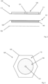
- Fig. 1 shows a schematic cross-sectional view of an antenna element 100 according to an embodiment of the present invention.
- the antenna element 100 comprises a first thin-film membrane 110, a second thin-film membrane 120, an electromagnetic metasurface 130, and a metallic coating 140.
- the second thin-film membrane 120 is arranged essentially parallel to and spaced apart from the first thin-film membrane 110.
- the electromagnetic metasurface 130 is arranged on a first side 111 of the first thin-film membrane 110 opposite of the second thin-film membrane 120.
- the metallic coating 140 is arranged on a first side 121 of the second thin-film membrane 120 opposite of the first thin-film membrane 110.
- the first thin-film layer 110 and the second thin-film layer 120 are separated from each other, the space between them filled either by air or any other atmosphere the antenna element is used in, or by vacuum, if the antenna element is used in space.
- the thin-film layers 110 and 120 and the space between serve as the dielectric medium between the electromagnetic metasurface 130 and the metal coating 140 which serves as a grounding plate. This way, the antenna element 100 can receive electromagnetic radiation.
- the thin-film membranes 110 and 120 are not further specified for this embodiment concerning their exact configurations and the materials used therein.
- the thin-film layer 110 and 120 can be configured in many ways depending on the specifics of the use-case for the antenna element 100.
- the antenna element 100 may be configured to be foldable. This is particularly advantageous for applications in space, where components should be designed with minimum space requirements, in particular during deployment of for example a satellite.
- the electromagnetic metasurface 130 may be configured to receive and/or emit microwave radiation. This wavelength range is particularly suited for the wireless transfer of energy over long distances.
- Fig. 2 shows a schematic cross-sectional view of an antenna element 100 according to an embodiment of the present invention.
- the antenna element 100 comprises all features of the antenna element shown in Fig. 1 .
- the electromagnetic metasurface 130 further comprises a feeding mechanism 131, which is configured to induce an emission of electromagnetic waves from the electromagnetic metasurface 130.
- the electromagnetic metasurface 130 induced by the feeding mechanism 131, can serve to emit electromagnetic radiation. It is not explicitly shown in Fig. 2 , how the feeding mechanism 131 is configured in detail. Fig. 2 shows one singular mechanism which could be understood to work as a feeding pin, however other mechanisms, e.g. slots and the like, can also be provided.
- FIG. 2 An additional, optional third thin-film membrane 150 is shown in Fig. 2 .
- the third thin-film membrane 150 is arranged essentially parallel to the first thin-film membrane 110 and the second thin-film membrane 120 on a side of the second thin-film membrane 120 opposite to the first thin-film membrane 110. In this way, the third thin-film membrane 150 can be useful for the implementation of various feeding mechanisms.
- the third thin-film membrane 150 could also be arranged on a side of the first thin-film membrane 110 opposite to the second thin-film membrane 120. Such a third thin-film membrane 150 could improve the electrical properties of the antenna element 100. Any number of third thin-film membranes 150 can be provided at both positions depending on the intended properties of the antenna element 100.
- Fig. 3 shows a schematic top view of an antenna element 100 according to an embodiment of the present invention.
- the antenna element 100 is configured the same way as the antenna element shown in Fig. 2 , wherein the first thin-film membrane 110, the electromagnetic metasurface 130 and the feeding mechanism 131 cane be seen in this view.
- the antenna element 100 further comprises a frame 150.
- the first thin-film membrane 110 and the second thin-film membrane, which is not shown, are attached to the frame 150.
- the frame 150 comprises a hexagonal form. This is one particular example of a form suited for regular tiling. In this way, a plurality of antenna elements 100 can be arranged in a lattice which covers substantially all of a given surface, as is for example indicated in Figure 3 . Other forms can also be used for this effect, for example the frame 150 may also comprise a square form. In order to facilitate this arrangement, the frame 150 may also be configured to connect to a frame 150 of an adjacent identical antenna element 100.
- the frame 150 may also comprise a circular shape, which might provide advantages with respect to the foldability of the antenna element 100.
- the frame 150 may also be configured to be foldable.
- Fig. 4 shows a schematic top view of an antenna array 10 according to an embodiment of the present invention.
- the antenna array 10 comprises a mounting device 11 and a plurality of antenna elements 100.
- the plurality of antenna elements 100 are attached to the mounting device 11.
- the mounting device 11 shown in Fig. 4 comprises a circular frame structure 12 which defines a planar area 13.
- the antenna elements 100 shown in Fig. 4 are configured the same way as the antenna element shown in Fig. 3 .
- the plurality of antenna elements 100 form a regular lattice arranged within the planar area 13.
- the plurality of antenna elements 100 does not cover the whole surface area of the planar are 13.
- the frame structure 12 comprises a mounting surface, which is not shown, to which the plurality of antenna elements 100 are attached.
- the plurality of antenna elements 100 might be attached directly to the frame structure 12, in particular in cases where the plurality of antenna elements 100 comprise frames which can be connected to one another.
- the mounting device 11 and frame structure 12 are not further defined for this embodiment, as there are many ways in which the mounting device 11 and frame structure 12 can be configured depending on the use-case of the antenna array 10. In particular the dimensions and materials used can be chosen according to the preferred properties of the antenna array 10.
- the mounting device 11 may be configured to be foldable. This is particularly advantageous for applications in space, where components should be designed with minimum space requirements, in particular during deployment of for example a satellite. In particular, the mounting device 11 can be configured to unfold itself and the antenna elements 100 all at the same time.
Landscapes
- Engineering & Computer Science (AREA)
- Aviation & Aerospace Engineering (AREA)
- Remote Sensing (AREA)
- Physics & Mathematics (AREA)
- Astronomy & Astrophysics (AREA)
- General Physics & Mathematics (AREA)
- Details Of Aerials (AREA)
- Aerials With Secondary Devices (AREA)
Abstract
The present invention is directed to an antenna element (100) comprising a first thin-film membrane (110); second thin-film membrane (120) arranged essentially parallel to and spaced apart from the first thin-film membrane (110); an electromagnetic metasurface (130) arranged on a first side (111) of the first thin-film membrane (110) opposite of the second thin-film membrane (120); and a metallic coating (140) arranged on a first side (121) of the second thin-film membrane (120) opposite of the first thin-film membrane (110). The present invention is further directed to an antenna array.
Description
- The present invention is directed to an antenna element and an antenna array.
- Layers consisting of usually periodic arrangements of subwavelength metallic inclusions in a dielectric host medium are referred to as metasurfaces. They can be designed to achieve unusual reflection/transmission properties of space waves and/or to modify the dispersion properties of surface/guided waves.
- In theory, such metasurfaces could be used to create antennas for the wireless transmission of energy via electromagnetic waves. This could be especially beneficial in the aerospace field, where energy transmission by wires is often not feasible, for example in order to power aircraft or even for satellites designed to collect solar power and transmit that power to Earth.
- However, the use of dielectric substrates in metasurface antennas limits their suitability for aerospace application, where weight and space requirements are often prohibitive.
- In view of the above, it is an objective of the present invention to provide antennas, in particular for the wireless transmission of energy, which have reduced weight, in particular for applications in space.
- This objective is achieved by an antenna element with the features of patent claim 1, and an antenna array with the features of
patent claim 12. - According to a first aspect of the invention, an antenna element comprising a first thin-film membrane, second thin-film membrane arranged essentially parallel to and spaced apart from the first thin-film membrane, an electromagnetic metasurface arranged on a first side of the first thin-film membrane opposite of the second thin-film membrane, and a metallic coating arranged on a first side of the second thin-film membrane opposite of the first thin-film membrane, is provided.
- According to a further aspect of the invention, an antenna array comprising a mounting device and a plurality of antenna elements according to the first aspect of the invention is provided. The plurality of antenna elements are attached to the mounting device.
- It is an idea of the invention to combine thin-film membranes and a metasurface in order to create an antenna, which can receive and emit radiation, depending on the specific embodiment, in particular for the purpose of wireless transmission of energy. This allows for a particularly light-weight antenna, which in turn allows the wireless transmission of energy in scenarios where conventional antennas used for the wireless transmission of energy might be not suited.
- According to a preferred embodiment of the antenna element, the electromagnetic metasurface comprises a feeding mechnism, which is configured to induce an emission of electromagnetic waves from the electromagnetic metasurface. In this way, the antenna element can be advantageously used for emitting electromagnetic radiation.
- According an embodiment of the present invention, the antenna element further comprises at least one third thin-film membrane arranged essentially parallel and spaced apart from the first thin-film membrane and the second thin-film membrane. These additional thin-film membranes can be advantageously used to adapt the antenna array to various purposes.
- According to a further embodiment of the antenna element, the at least one third thin-film membrane is arranged on a side of the first thin-film membrane opposite to the second thin-film membrane. This can advantageously improve the electrical properties of the antenna element.
- According to a further embodiment of the antenna element, the at least one third thin-film membrane is arranged on a side of the second thin-film membrane opposite to the first thin-film membrane. This can advantageously allow the implementation of various feeding mechanisms.
- According to a further embodiment of the present invention, the antenna element is configured to be foldable. This advantageously reduces the space requirements of the antenna element, in particular during deployment for use in space.
- According to a further embodiment of the antenna element, the electromagnetic metasurface is configured to receive and/or emit microwave radiation. This wavelength range is particularly advantageous for the wireless transmission of energy over long distances.
- According to a further embodiment, the antenna element further comprises a frame, wherein the first thin-film membrane and the second thin-film membrane are attached to the frame. This advantageously increases the stability of the antenna element.
- According to a further embodiment, the frame comprises a form suited for regular tiling. This allows the antenna element to be used to efficiently cover a surface when used in multiples.
- According to a further embodiment, the frame comprises a hexagonal form or a square form. This are particularly simple examples of forms used for regular tiling.
- According to a further embodiment, the frame is configured to connect to a frame of an adjacent identical antenna element. This is particularly advantageous when deploying multiple antenna elements in conjunction.
- According to a further embodiment of the antenna array, the mounting device is configured to be foldable. This advantageously reduces the space requirements of the antenna array, in particular during deployment for use in space.
- According to a further embodiment of the antenna array, the mounting device comprises a frame structure which defines a planar area. This advantageously increases the stability of the antenna array.
- According to a further embodiment, the plurality of antenna elements cover substantially the entirety of the planar area. This advantageously increases the efficiency of the antenna array per surface.
- The present invention is explained in more detail below with reference to the embodiments shown in the schematic figures:
- Fig. 1
- shows a schematic cross-sectional view of an antenna element according to an embodiment of the present invention;
- Fig. 2
- shows a schematic cross-sectional view of an antenna element according to an embodiment of the present invention;
- Fig. 3
- shows a schematic top view of an antenna element according to an embodiment of the present invention; and
- Fig. 4
- shows a schematic top view of an antenna array according to an embodiment of the present invention.
- In the figures of the drawing, elements, features and components which are identical, functionally identical and of identical action are denoted in each case by the same reference designations unless stated otherwise.
-
Fig. 1 shows a schematic cross-sectional view of anantenna element 100 according to an embodiment of the present invention. - The
antenna element 100 comprises a first thin-film membrane 110, a second thin-film membrane 120, anelectromagnetic metasurface 130, and ametallic coating 140. The second thin-film membrane 120 is arranged essentially parallel to and spaced apart from the first thin-film membrane 110. Theelectromagnetic metasurface 130 is arranged on afirst side 111 of the first thin-film membrane 110 opposite of the second thin-film membrane 120. Themetallic coating 140 is arranged on afirst side 121 of the second thin-film membrane 120 opposite of the first thin-film membrane 110. - The first thin-
film layer 110 and the second thin-film layer 120 are separated from each other, the space between them filled either by air or any other atmosphere the antenna element is used in, or by vacuum, if the antenna element is used in space. In both cases, the thin-film layers electromagnetic metasurface 130 and themetal coating 140 which serves as a grounding plate. This way, theantenna element 100 can receive electromagnetic radiation. - The thin-
film membranes film layer antenna element 100. In a particularly preferred embodiment, theantenna element 100 may be configured to be foldable. This is particularly advantageous for applications in space, where components should be designed with minimum space requirements, in particular during deployment of for example a satellite. - The same way, the specifics of the design of the
electromagnetic metasurface 130 are not presented in this embodiment, as there are many ways in which theelectromagnetic metasurface 130 can be designed, depending on the use-case of the antenna element. In particular, the sizes, arrangements and materials used for the elements which make up the metasurface can be chosen according to the desired properties of theantenna element 100. In one particularly preferred embodiment, theelectromagnetic metasurface 130 may configured to receive and/or emit microwave radiation. This wavelength range is particularly suited for the wireless transfer of energy over long distances. -
Fig. 2 shows a schematic cross-sectional view of anantenna element 100 according to an embodiment of the present invention. - The
antenna element 100 comprises all features of the antenna element shown inFig. 1 . Theelectromagnetic metasurface 130 further comprises afeeding mechanism 131, which is configured to induce an emission of electromagnetic waves from theelectromagnetic metasurface 130. - In this embodiment, the
electromagnetic metasurface 130, induced by thefeeding mechanism 131, can serve to emit electromagnetic radiation. It is not explicitly shown inFig. 2 , how thefeeding mechanism 131 is configured in detail.Fig. 2 shows one singular mechanism which could be understood to work as a feeding pin, however other mechanisms, e.g. slots and the like, can also be provided. - An additional, optional third thin-
film membrane 150 is shown inFig. 2 . The third thin-film membrane 150 is arranged essentially parallel to the first thin-film membrane 110 and the second thin-film membrane 120 on a side of the second thin-film membrane 120 opposite to the first thin-film membrane 110. In this way, the third thin-film membrane 150 can be useful for the implementation of various feeding mechanisms. The third thin-film membrane 150 could also be arranged on a side of the first thin-film membrane 110 opposite to the second thin-film membrane 120. Such a third thin-film membrane 150 could improve the electrical properties of theantenna element 100. Any number of third thin-film membranes 150 can be provided at both positions depending on the intended properties of theantenna element 100. -
Fig. 3 shows a schematic top view of anantenna element 100 according to an embodiment of the present invention. - The
antenna element 100 is configured the same way as the antenna element shown inFig. 2 , wherein the first thin-film membrane 110, theelectromagnetic metasurface 130 and thefeeding mechanism 131 cane be seen in this view. Theantenna element 100 further comprises aframe 150. - The first thin-
film membrane 110 and the second thin-film membrane, which is not shown, are attached to theframe 150. - In the embodiment shown, the
frame 150 comprises a hexagonal form. This is one particular example of a form suited for regular tiling. In this way, a plurality ofantenna elements 100 can be arranged in a lattice which covers substantially all of a given surface, as is for example indicated inFigure 3 . Other forms can also be used for this effect, for example theframe 150 may also comprise a square form. In order to facilitate this arrangement, theframe 150 may also be configured to connect to aframe 150 of an adjacentidentical antenna element 100. - Alternatively, the
frame 150 may also comprise a circular shape, which might provide advantages with respect to the foldability of theantenna element 100. - The
frame 150 may also be configured to be foldable. -
Fig. 4 shows a schematic top view of anantenna array 10 according to an embodiment of the present invention. - The
antenna array 10 comprises a mountingdevice 11 and a plurality ofantenna elements 100. The plurality ofantenna elements 100 are attached to the mountingdevice 11. The mountingdevice 11 shown inFig. 4 comprises acircular frame structure 12 which defines aplanar area 13. - The
antenna elements 100 shown inFig. 4 are configured the same way as the antenna element shown inFig. 3 . The plurality ofantenna elements 100, of which four are shown inFig. 4 , form a regular lattice arranged within theplanar area 13. In the embodiment shown, the plurality ofantenna elements 100 does not cover the whole surface area of the planar are 13. This implies that theframe structure 12 comprises a mounting surface, which is not shown, to which the plurality ofantenna elements 100 are attached. In cases where the plurality ofantenna elements 100 are arranged to cover the entirety of theplanar area 13, the plurality ofantenna elements 100 might be attached directly to theframe structure 12, in particular in cases where the plurality ofantenna elements 100 comprise frames which can be connected to one another. - The specifics of the mounting
device 11, and in particular theframe structure 12 are not further defined for this embodiment, as there are many ways in which the mountingdevice 11 andframe structure 12 can be configured depending on the use-case of theantenna array 10. In particular the dimensions and materials used can be chosen according to the preferred properties of theantenna array 10. In a particularly preferred embodiment, the mountingdevice 11 may be configured to be foldable. This is particularly advantageous for applications in space, where components should be designed with minimum space requirements, in particular during deployment of for example a satellite. In particular, the mountingdevice 11 can be configured to unfold itself and theantenna elements 100 all at the same time. -
- 10
- antenna array
- 11
- mounting device
- 12
- frame structure
- 13
- planar area
- 100
- antenna element
- 110
- first thin-film membrane
- 111
- first side
- 120
- second thin-film membrane
- 121
- first side
- 130
- electromagnetic metasurface
- 131
- feeding mechanism
- 140
- metallic coating
- 150
- frame
Claims (15)
- Antenna element (100) comprisinga first thin-film membrane (110);second thin-film membrane (120) arranged essentially parallel to and spaced apart from the first thin-film membrane (110);an electromagnetic metasurface (130) arranged on a first side (111) of the first thin-film membrane (110) opposite of the second thin-film membrane (120); anda metallic coating (140) arranged on a first side (121) of the second thin-film membrane (120) opposite of the first thin-film membrane (110).
- Antenna element (100) according to claim 1, wherein the electromagnetic metasurface (130) comprises a feeding mechanism (131), which is configured to induce an emission of electromagnetic waves from the electromagnetic metasurface (130).
- Antenna element (100) according to any one of claims 1 or 2, further comprising at least one third thin-film membrane (150) arranged essentially parallel and spaced apart from the first thin-film membrane (110) and the second thin-film membrane (120).
- Antenna element (100) according to claim 3, wherein the at least one third thin-film membrane (150) is arranged on a side of the first thin-film membrane (110) opposite to the second thin-film membrane (120).
- Antenna element (100) according to any one of claims 3 or 4, wherein the at least one third thin-film membrane (150) is arranged on a side of the second thin-film membrane (120) opposite to the first thin-film membrane (110).
- Antenna element (100) according to any one of the preceding claims,
wherein the antenna element (100) is configured to be foldable. - Antenna element (100) according to any one of the preceding claims,
wherein the electromagnetic metasurface (130) is configured to receive and/or emit microwave radiation. - Antenna element (100) according to any one of the preceding claims, further comprising a frame (150), wherein the first thin-film membrane (110) and the second thin-film membrane (120) are attached to the frame (150).
- Antenna element (100) according to claim 8, wherein the frame (150) comprises a form suited for regular tiling.
- Antenna element (100) according to claim 9, wherein the frame (150) comprises a hexagonal form or a square form.
- Antenna element (100) according to any one of claims 8 to 10, wherein the frame (150) is configured to connect to a frame (150) of an adjacent identical antenna element (100).
- Antenna array (10) comprising a mounting device (11) and a plurality of antenna elements (100) according to any one of claims 1 to 11, wherein the plurality of antenna elements (100) are attached to the mounting device (11).
- Antenna array (10) according to claim 12, wherein the mounting device (11) is configured to be foldable.
- Antenna array (10) according to any one of claims 12 or 13, wherein the mounting device (11) comprises a frame structure (12) which defines a planar area (13).
- Antenna array (10) according to claim 14, wherein the plurality of antenna elements (100) cover substantially the entirety of the planar area (13).
Priority Applications (3)
| Application Number | Priority Date | Filing Date | Title |
|---|---|---|---|
| EP23172064.0A EP4462591A1 (en) | 2023-05-08 | 2023-05-08 | Antenna element and antenna array |
| US18/655,585 US20240380119A1 (en) | 2023-05-08 | 2024-05-06 | Antenna element and antenna array |
| CN202410560101.8A CN118920077A (en) | 2023-05-08 | 2024-05-08 | Antenna element and antenna array |
Applications Claiming Priority (1)
| Application Number | Priority Date | Filing Date | Title |
|---|---|---|---|
| EP23172064.0A EP4462591A1 (en) | 2023-05-08 | 2023-05-08 | Antenna element and antenna array |
Publications (1)
| Publication Number | Publication Date |
|---|---|
| EP4462591A1 true EP4462591A1 (en) | 2024-11-13 |
Family
ID=86330343
Family Applications (1)
| Application Number | Title | Priority Date | Filing Date |
|---|---|---|---|
| EP23172064.0A Pending EP4462591A1 (en) | 2023-05-08 | 2023-05-08 | Antenna element and antenna array |
Country Status (3)
| Country | Link |
|---|---|
| US (1) | US20240380119A1 (en) |
| EP (1) | EP4462591A1 (en) |
| CN (1) | CN118920077A (en) |
Citations (4)
| Publication number | Priority date | Publication date | Assignee | Title |
|---|---|---|---|---|
| US6091367A (en) * | 1997-09-30 | 2000-07-18 | Mitsubishi Denki Kabushiki Kaisha | Light-weight flat antenna device tolerant of temperature variation |
| CN112768911A (en) * | 2020-12-29 | 2021-05-07 | 中山大学 | Rectangular patch array staggered super-surface antenna |
| CN114914698A (en) * | 2022-05-30 | 2022-08-16 | 湖北汽车工业学院 | Design method of coating type double-frequency millimeter wave metamaterial divinatory microstrip antenna |
| US20220384954A1 (en) * | 2019-11-14 | 2022-12-01 | Nissha Co., Ltd. | Cover with antenna function |
Family Cites Families (1)
| Publication number | Priority date | Publication date | Assignee | Title |
|---|---|---|---|---|
| EP4418460A4 (en) * | 2021-10-15 | 2024-12-04 | Beijing Xiaomi Mobile Software Co., Ltd. | ANTENNA NETWORK AND COMMUNICATION DEVICE |
-
2023
- 2023-05-08 EP EP23172064.0A patent/EP4462591A1/en active Pending
-
2024
- 2024-05-06 US US18/655,585 patent/US20240380119A1/en active Pending
- 2024-05-08 CN CN202410560101.8A patent/CN118920077A/en active Pending
Patent Citations (4)
| Publication number | Priority date | Publication date | Assignee | Title |
|---|---|---|---|---|
| US6091367A (en) * | 1997-09-30 | 2000-07-18 | Mitsubishi Denki Kabushiki Kaisha | Light-weight flat antenna device tolerant of temperature variation |
| US20220384954A1 (en) * | 2019-11-14 | 2022-12-01 | Nissha Co., Ltd. | Cover with antenna function |
| CN112768911A (en) * | 2020-12-29 | 2021-05-07 | 中山大学 | Rectangular patch array staggered super-surface antenna |
| CN114914698A (en) * | 2022-05-30 | 2022-08-16 | 湖北汽车工业学院 | Design method of coating type double-frequency millimeter wave metamaterial divinatory microstrip antenna |
Non-Patent Citations (2)
| Title |
|---|
| KOMSAN KANJANASIT ET AL: "A high directivity broadband aperture coupled patch antenna using a metamaterial based superstrate", ANTENNAS AND PROPAGATION CONFERENCE (LAPC), 2012 LOUGHBOROUGH, IEEE, 12 November 2012 (2012-11-12), pages 1 - 4, XP032299105, ISBN: 978-1-4673-2218-8, DOI: 10.1109/LAPC.2012.6403004 * |
| MOUSSESSIAN ALINA ET AL: "Architectural study of active membrane antennas", 2002 9TH INTERNATIONAL SYMPOSIUM ON ANTENNA TECHNOLOGY AND APPLIED ELECTROMAGNETICS [ANTEM], IEEE, 31 July 2002 (2002-07-31), pages 1 - 4, XP033072034, ISBN: 978-0-9692563-8-0, [retrieved on 20170224] * |
Also Published As
| Publication number | Publication date |
|---|---|
| CN118920077A (en) | 2024-11-08 |
| US20240380119A1 (en) | 2024-11-14 |
Similar Documents
| Publication | Publication Date | Title |
|---|---|---|
| US7154451B1 (en) | Large aperture rectenna based on planar lens structures | |
| CN106450765B (en) | A kind of millimeter wave reconfigurable antenna | |
| US4943811A (en) | Dual polarization electromagnetic power reception and conversion system | |
| EP3149777B1 (en) | Large-scale space-based solar power station: efficient power generation tiles | |
| CN106848558B (en) | Solar sailboard conformal antenna of spacecraft | |
| US20170110803A1 (en) | Deployable reflectarray high gain antenna for satellite applications | |
| JPH0799409A (en) | Duplex polarized wave dipole group antenna | |
| US12288933B2 (en) | Antenna system for satellite applications | |
| Zawadzki et al. | Integrated RF antenna and solar array for spacecraft application | |
| US11658398B1 (en) | Lightweight conformal phased array antenna using aerogel substrate | |
| US20170025992A1 (en) | Mirrors Transparent to Specific Regions of the Electromagnetic Spectrum | |
| EP2664029B1 (en) | Printed circuit board based feed horn | |
| US11923618B2 (en) | Digital conformal antenna | |
| US20240145905A1 (en) | Base station antennas having light weight multi-layer composite frequency selective surfaces | |
| Thandullu Naganathan et al. | Patch antenna integrated on solar cells for green wireless communication: A feature oriented survey and design issues | |
| EP3764463B1 (en) | Deployable horn antenna and associated methods | |
| US20240380119A1 (en) | Antenna element and antenna array | |
| JP2014003436A (en) | Antenna device using ebg structure | |
| EP2853005A1 (en) | Lightweight stiffener with integrated rf cavity-backed radiator for flexible rf emitters | |
| WO2024250162A1 (en) | A dielectric and conductive foil based distribution network with bendable feeding probes | |
| JP5665028B2 (en) | Transmit antenna | |
| US10931022B1 (en) | Reconfigurable arrays with multiple unit cells | |
| US11005189B2 (en) | Technique for reconstruction of radiation patterns for antennas working in close proximity of conductive bodies | |
| JP2006311421A (en) | Polarization converter and antenna device using the same | |
| Gopika et al. | Differential loop rectenna unit for extendable large arrays |
Legal Events
| Date | Code | Title | Description |
|---|---|---|---|
| PUAI | Public reference made under article 153(3) epc to a published international application that has entered the european phase |
Free format text: ORIGINAL CODE: 0009012 |
|
| STAA | Information on the status of an ep patent application or granted ep patent |
Free format text: STATUS: REQUEST FOR EXAMINATION WAS MADE |
|
| 17P | Request for examination filed |
Effective date: 20240624 |
|
| AK | Designated contracting states |
Kind code of ref document: A1 Designated state(s): AL AT BE BG CH CY CZ DE DK EE ES FI FR GB GR HR HU IE IS IT LI LT LU LV MC ME MK MT NL NO PL PT RO RS SE SI SK SM TR |