EP4462485A1 - Lateral diode for backside power rail application - Google Patents
Lateral diode for backside power rail application Download PDFInfo
- Publication number
- EP4462485A1 EP4462485A1 EP24172734.6A EP24172734A EP4462485A1 EP 4462485 A1 EP4462485 A1 EP 4462485A1 EP 24172734 A EP24172734 A EP 24172734A EP 4462485 A1 EP4462485 A1 EP 4462485A1
- Authority
- EP
- European Patent Office
- Prior art keywords
- well
- structures
- semiconductor
- type doped
- contacts
- Prior art date
- Legal status (The legal status is an assumption and is not a legal conclusion. Google has not performed a legal analysis and makes no representation as to the accuracy of the status listed.)
- Pending
Links
Images


Classifications
-
- H—ELECTRICITY
- H10—SEMICONDUCTOR DEVICES; ELECTRIC SOLID-STATE DEVICES NOT OTHERWISE PROVIDED FOR
- H10D—INORGANIC ELECTRIC SEMICONDUCTOR DEVICES
- H10D8/00—Diodes
-
- H—ELECTRICITY
- H10—SEMICONDUCTOR DEVICES; ELECTRIC SOLID-STATE DEVICES NOT OTHERWISE PROVIDED FOR
- H10W—GENERIC PACKAGES, INTERCONNECTIONS, CONNECTORS OR OTHER CONSTRUCTIONAL DETAILS OF DEVICES COVERED BY CLASS H10
- H10W20/00—Interconnections in chips, wafers or substrates
- H10W20/40—Interconnections external to wafers or substrates, e.g. back-end-of-line [BEOL] metallisations or vias connecting to gate electrodes
- H10W20/41—Interconnections external to wafers or substrates, e.g. back-end-of-line [BEOL] metallisations or vias connecting to gate electrodes characterised by their conductive parts
- H10W20/427—Power or ground buses
-
- H—ELECTRICITY
- H10—SEMICONDUCTOR DEVICES; ELECTRIC SOLID-STATE DEVICES NOT OTHERWISE PROVIDED FOR
- H10D—INORGANIC ELECTRIC SEMICONDUCTOR DEVICES
- H10D62/00—Semiconductor bodies, or regions thereof, of devices having potential barriers
- H10D62/10—Shapes, relative sizes or dispositions of the regions of the semiconductor bodies; Shapes of the semiconductor bodies
- H10D62/113—Isolations within a component, i.e. internal isolations
- H10D62/115—Dielectric isolations, e.g. air gaps
-
- H—ELECTRICITY
- H10—SEMICONDUCTOR DEVICES; ELECTRIC SOLID-STATE DEVICES NOT OTHERWISE PROVIDED FOR
- H10D—INORGANIC ELECTRIC SEMICONDUCTOR DEVICES
- H10D62/00—Semiconductor bodies, or regions thereof, of devices having potential barriers
- H10D62/10—Shapes, relative sizes or dispositions of the regions of the semiconductor bodies; Shapes of the semiconductor bodies
- H10D62/124—Shapes, relative sizes or dispositions of the regions of semiconductor bodies or of junctions between the regions
- H10D62/126—Top-view geometrical layouts of the regions or the junctions
-
- H—ELECTRICITY
- H10—SEMICONDUCTOR DEVICES; ELECTRIC SOLID-STATE DEVICES NOT OTHERWISE PROVIDED FOR
- H10D—INORGANIC ELECTRIC SEMICONDUCTOR DEVICES
- H10D64/00—Electrodes of devices having potential barriers
- H10D64/01—Manufacture or treatment
- H10D64/017—Manufacture or treatment using dummy gates in processes wherein at least parts of the final gates are self-aligned to the dummy gates, i.e. replacement gate processes
-
- H—ELECTRICITY
- H10—SEMICONDUCTOR DEVICES; ELECTRIC SOLID-STATE DEVICES NOT OTHERWISE PROVIDED FOR
- H10D—INORGANIC ELECTRIC SEMICONDUCTOR DEVICES
- H10D64/00—Electrodes of devices having potential barriers
- H10D64/20—Electrodes characterised by their shapes, relative sizes or dispositions
- H10D64/23—Electrodes carrying the current to be rectified, amplified, oscillated or switched, e.g. sources, drains, anodes or cathodes
- H10D64/251—Source or drain electrodes for field-effect devices
- H10D64/256—Source or drain electrodes for field-effect devices for lateral devices wherein the source or drain electrodes are recessed in semiconductor bodies
-
- H—ELECTRICITY
- H10—SEMICONDUCTOR DEVICES; ELECTRIC SOLID-STATE DEVICES NOT OTHERWISE PROVIDED FOR
- H10D—INORGANIC ELECTRIC SEMICONDUCTOR DEVICES
- H10D8/00—Diodes
- H10D8/411—PN diodes having planar bodies
-
- H—ELECTRICITY
- H10—SEMICONDUCTOR DEVICES; ELECTRIC SOLID-STATE DEVICES NOT OTHERWISE PROVIDED FOR
- H10D—INORGANIC ELECTRIC SEMICONDUCTOR DEVICES
- H10D89/00—Aspects of integrated devices not covered by groups H10D84/00 - H10D88/00
- H10D89/10—Integrated device layouts
-
- H—ELECTRICITY
- H10—SEMICONDUCTOR DEVICES; ELECTRIC SOLID-STATE DEVICES NOT OTHERWISE PROVIDED FOR
- H10D—INORGANIC ELECTRIC SEMICONDUCTOR DEVICES
- H10D89/00—Aspects of integrated devices not covered by groups H10D84/00 - H10D88/00
- H10D89/60—Integrated devices comprising arrangements for electrical or thermal protection, e.g. protection circuits against electrostatic discharge [ESD]
-
- H—ELECTRICITY
- H10—SEMICONDUCTOR DEVICES; ELECTRIC SOLID-STATE DEVICES NOT OTHERWISE PROVIDED FOR
- H10D—INORGANIC ELECTRIC SEMICONDUCTOR DEVICES
- H10D64/00—Electrodes of devices having potential barriers
- H10D64/111—Field plates
-
- H—ELECTRICITY
- H10—SEMICONDUCTOR DEVICES; ELECTRIC SOLID-STATE DEVICES NOT OTHERWISE PROVIDED FOR
- H10D—INORGANIC ELECTRIC SEMICONDUCTOR DEVICES
- H10D84/00—Integrated devices formed in or on semiconductor substrates that comprise only semiconducting layers, e.g. on Si wafers or on GaAs-on-Si wafers
- H10D84/01—Manufacture or treatment
- H10D84/0123—Integrating together multiple components covered by H10D12/00 or H10D30/00, e.g. integrating multiple IGBTs
- H10D84/0126—Integrating together multiple components covered by H10D12/00 or H10D30/00, e.g. integrating multiple IGBTs the components including insulated gates, e.g. IGFETs
- H10D84/0149—Manufacturing their interconnections or electrodes, e.g. source or drain electrodes
-
- H—ELECTRICITY
- H10—SEMICONDUCTOR DEVICES; ELECTRIC SOLID-STATE DEVICES NOT OTHERWISE PROVIDED FOR
- H10D—INORGANIC ELECTRIC SEMICONDUCTOR DEVICES
- H10D84/00—Integrated devices formed in or on semiconductor substrates that comprise only semiconducting layers, e.g. on Si wafers or on GaAs-on-Si wafers
- H10D84/01—Manufacture or treatment
- H10D84/02—Manufacture or treatment characterised by using material-based technologies
- H10D84/03—Manufacture or treatment characterised by using material-based technologies using Group IV technology, e.g. silicon technology or silicon-carbide [SiC] technology
- H10D84/038—Manufacture or treatment characterised by using material-based technologies using Group IV technology, e.g. silicon technology or silicon-carbide [SiC] technology using silicon technology, e.g. SiGe
Definitions
- a power delivery network is designed to provide power supply and reference voltage to the active devices on the die most efficiently. Traditionally, it is realized as a network of low-resistive metal wires fabricated through back-end-of-line (BEOL) processing on the front-side of the wafer. The power delivery network shares this space with the signal network.
- BEOL back-end-of-line
- a backside power delivery is developed to eliminate the need to share interconnect resources between signal and power lines on the front-side of the wafer. Instead, the power line is moved to the back of the wafer so only signals are carried by front-side interconnects.
- a silicon substrate will be thinning by polish, and a conventional diode may have no suitable current path for current transport.
- the conventional diode may have a P+ epitaxy and a N+ epitaxy positioned on different oxide definitions, and a current path is formed from the P+ epitaxy, N-well or P-well to the N+ epitaxy. If the wafer is polished very thin, the N-well/P-well connections between different operation domains will be cut off, causing the current path of the diode to disappear.
- a semiconductor structure comprising an oxide definition region, a plurality of metal gate structures and a plurality of S/D contacts.
- the oxide definition region is disposed over a semiconductor substrate and surrounded by insulating regions.
- the plurality of metal gate structures are disposed on an N-well or a P-well manufactured on the semiconductor substrate.
- the plurality of S/D contacts are disposed on the N-well or the P-well manufactured on the semiconductor substrate.
- the plurality of metal gate structures, the plurality of S/D contacts and the at least one dummy gate structure are within the oxide definition region.
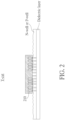
- FIG. 1 - FIG. 3 are cross-section views of a lateral diode 100 according to one embodiment of the present invention, wherein FIG. 1 shows a top view (Z-direction) of the lateral diode 100, FIG. 2 shows a cross-section view of the Y-cut, and FIG. 3 shows a cross-section view of the X-cut.
- a plurality source/drain (S/D) contacts (MD) and a plurality of metal gate structure (MG) are formed on a N-well or P-well manufactured on a semiconductor substrate such as silicon substrate, wherein the S/D contacts and metal gate structures are arranged in parallel and alternately.
- the S/D contacts comprise source contacts and drain contacts, and the source contacts and the drain contacts are separated by a dummy gate structure, wherein the dummy gate structure is generally called an oxide definition edge (CPODE) pattern, and the dummy gate structure can serve as an insulating region manufactured by using silicon oxide, silicon nitride or silicon oxynitride.
- the source contacts and the drain contacts are all manufactured on the same oxide definition (OD) 110.
- a continuous poly on the CPODE pattern is used to form a trench by removing a dummy structure and a portion of a substrate under the dummy structure.
- the term "oxide definition (OD)" is an active region for a semiconductor device such as a transistor or the lateral diode 100, i.e., the area where a source, a drain, and a channel under a gate of the transistor are formed.
- the OD region is disposed over the semiconductor substrate and is between insulating regions, wherein the insulating regions are also called inactive regions or isolation regions.
- the insulating regions are shallow trench isolation (STI), field oxide (FOX) areas, or other suitable electrically insulating structures.
- the source/drain (S/D) contacts shown in FIG. 2 comprise metal layer and a plurality of epitaxial layer of N-doped or P-doped 210.
- the P-type epitaxial material may include one or more epitaxial layers of silicon germanium (epi SiGe) doped with a P-type dopant such as boron, gallium, indium, and/or other P-type dopants.
- the N-type epitaxial material may include one or more epitaxial layers of silicon (epi Si) or silicon carbon (epi SiC) doped with an N-type dopant such as arsenic, phosphorus, and/or other n-type dopant.
- the lateral diode 100 is manufactured on the same OD surrounded by the insulating regions 310_1 and 310_2, wherein the insulating regions 310_1 and 310_2 may include silicon oxide, silicon nitride, silicon oxynitride, fluoride-doped silicate glass (FSG), a low-k dielectric material, other suitable materials, or combinations thereof.
- the insulating regions 310_1 and 310_2 may include silicon oxide, silicon nitride, silicon oxynitride, fluoride-doped silicate glass (FSG), a low-k dielectric material, other suitable materials, or combinations thereof.
- the lateral diode 100 comprises a plurality of first structures 320_1 and 320_2, a plurality of second structures 330_1 - 330_6, a plurality of dummy gate structures 340_1 and 340_2, and a plurality of metal gate structures 350_1 - 350_5 manufactured on the N-well or the P-well.
- the first structures 320_1 and 320_2 are included in source contacts or drain contacts, and the first structures 320_1 and 320_2 are positioned near the edge of the OD, that is the first structure 320_1 is positioned between the insulating region 310_1 and the dummy gate structure 340_1, and the first structure 320_2 is positioned between the insulating region 310_2 and the dummy gate structure 340_2.
- the second structures 330_1 - 330_6 are included in source contacts or drain contacts different from the first structures 320_1 and 320_2, and the second structures 330_1 - 330_6 are positioned between the dummy gate structures 340_1 and 340_2.
- the first structures 320_1 and 320_2 and the second structures 330_1 - 330_6 are manufactured by epitaxial growth, and the first structures 320_1 and 320_2 and the second structures 330_1 - 330_6 are epitaxial layers with different type of doped materials.
- the first structures 320_1 and 320_2 may be formed by the epitaxial layer of P-type epitaxial material, and the second structures 330_1 - 330_6 may be formed by the epitaxial layer of N-type epitaxial material.
- first structures 320_1 and 320_2 may be formed by the epitaxial layer of N-type epitaxial material
- the second structures 330_1 - 330_6 may be formed by the epitaxial layer of P-type epitaxial material.
- a current path can be formed to between the first structures 320_1 and 320_2 and the second structures 330_1 - 330_6 through the N-well or P-well below.
- first structures 320_1 and 320_2 have the N-type epitaxial material and the second structures 330_1 - 330_6 have the P-type epitaxial material, a current is flowing from the second structures 330_1 - 330_6 to the first structures 320_1 and 320_2 through the N-well or P-well.
- first structures 320_1 and 320_2 have the P-type epitaxial material and the second structures 330_1 - 330_6 have the N-type epitaxial material, a current is flowing from the first structures 320_1 and 320_2 to the second structures 330_1 - 330_6 through the N-well or P-well.
- the semiconductor device can still provide a current path in the X direction so that the lateral diode 100 can operate smoothly.
Landscapes
- Electrodes Of Semiconductors (AREA)
- Insulated Gate Type Field-Effect Transistor (AREA)
Abstract
Description
- This application claims the benefit of
U.S. Provisional Application No. 63/464,930, filed on May 8th, 2023 - A power delivery network is designed to provide power supply and reference voltage to the active devices on the die most efficiently. Traditionally, it is realized as a network of low-resistive metal wires fabricated through back-end-of-line (BEOL) processing on the front-side of the wafer. The power delivery network shares this space with the signal network.
- When the semiconductor process technology keeps scaling, BEOL capacitance and IR drop becomes serious and degrade the chip performance. In order to solve these problems, a backside power delivery is developed to eliminate the need to share interconnect resources between signal and power lines on the front-side of the wafer. Instead, the power line is moved to the back of the wafer so only signals are carried by front-side interconnects.
- However, for the wafer having backside power delivery design, a silicon substrate will be thinning by polish, and a conventional diode may have no suitable current path for current transport. In detail, the conventional diode may have a P+ epitaxy and a N+ epitaxy positioned on different oxide definitions, and a current path is formed from the P+ epitaxy, N-well or P-well to the N+ epitaxy. If the wafer is polished very thin, the N-well/P-well connections between different operation domains will be cut off, causing the current path of the diode to disappear.
- It is therefore an objective of the present invention to provide a diode design, which has one directional current path for the backside power delivery applications, to solve the above-mentioned problems.
- According to one embodiment of the present invention, a semiconductor structure is disclosed. The semiconductor structure comprises an oxide definition region, a plurality of metal gate structures and a plurality of S/D contacts. The oxide definition region is disposed over a semiconductor substrate and surrounded by insulating regions. The plurality of metal gate structures are disposed on an N-well or a P-well manufactured on the semiconductor substrate. The plurality of S/D contacts are disposed on the N-well or the P-well manufactured on the semiconductor substrate. In addition, the plurality of metal gate structures, the plurality of S/D contacts and the at least one dummy gate structure are within the oxide definition region.
- These and other objectives of the present invention will no doubt become obvious to those of ordinary skill in the art after reading the following detailed description of the preferred embodiment that is illustrated in the various figures and drawings.
-
-
FIG. 1 shows a top view of a lateral diode according to one embodiment of the present invention. -
FIG. 2 shows a cross-section view of the Y-cut according to one embodiment of the present invention. -
FIG. 3 shows a cross-section view of the X-cut according to one embodiment of the present invention. - Certain terms are used throughout the following description and claims to refer to particular system components. As one skilled in the art will appreciate, manufacturers may refer to a component by different names. This document does not intend to distinguish between components that differ in name but not function. In the following discussion and in the claims, the terms "including" and "comprising" are used in an open-ended fashion, and thus should be interpreted to mean "including, but not limited to ...". The terms "couple" and "couples" are intended to mean either an indirect or a direct electrical connection. Thus, if a first device couples to a second device, that connection may be through a direct electrical connection, or through an indirect electrical connection via other devices and connections.
-
FIG. 1 - FIG. 3 are cross-section views of alateral diode 100 according to one embodiment of the present invention, whereinFIG. 1 shows a top view (Z-direction) of thelateral diode 100,FIG. 2 shows a cross-section view of the Y-cut, andFIG. 3 shows a cross-section view of the X-cut. - In
FIG. 1 , a plurality source/drain (S/D) contacts (MD) and a plurality of metal gate structure (MG) are formed on a N-well or P-well manufactured on a semiconductor substrate such as silicon substrate, wherein the S/D contacts and metal gate structures are arranged in parallel and alternately. In this embodiment, the S/D contacts comprise source contacts and drain contacts, and the source contacts and the drain contacts are separated by a dummy gate structure, wherein the dummy gate structure is generally called an oxide definition edge (CPODE) pattern, and the dummy gate structure can serve as an insulating region manufactured by using silicon oxide, silicon nitride or silicon oxynitride. In addition, the source contacts and the drain contacts are all manufactured on the same oxide definition (OD) 110. - A continuous poly on the CPODE pattern is used to form a trench by removing a dummy structure and a portion of a substrate under the dummy structure. In at least one example, the term "oxide definition (OD)" is an active region for a semiconductor device such as a transistor or the
lateral diode 100, i.e., the area where a source, a drain, and a channel under a gate of the transistor are formed. In some examples, the OD region is disposed over the semiconductor substrate and is between insulating regions, wherein the insulating regions are also called inactive regions or isolation regions. In some embodiments, the insulating regions are shallow trench isolation (STI), field oxide (FOX) areas, or other suitable electrically insulating structures. - The source/drain (S/D) contacts shown in
FIG. 2 comprise metal layer and a plurality of epitaxial layer of N-doped or P-doped 210. In some embodiments, the P-type epitaxial material may include one or more epitaxial layers of silicon germanium (epi SiGe) doped with a P-type dopant such as boron, gallium, indium, and/or other P-type dopants. The N-type epitaxial material may include one or more epitaxial layers of silicon (epi Si) or silicon carbon (epi SiC) doped with an N-type dopant such as arsenic, phosphorus, and/or other n-type dopant. - In the cross-section view of the X-cut shown in
FIG. 3 , thelateral diode 100 is manufactured on the same OD surrounded by the insulating regions 310_1 and 310_2, wherein the insulating regions 310_1 and 310_2 may include silicon oxide, silicon nitride, silicon oxynitride, fluoride-doped silicate glass (FSG), a low-k dielectric material, other suitable materials, or combinations thereof. Thelateral diode 100 comprises a plurality of first structures 320_1 and 320_2, a plurality of second structures 330_1 - 330_6, a plurality of dummy gate structures 340_1 and 340_2, and a plurality of metal gate structures 350_1 - 350_5 manufactured on the N-well or the P-well. The first structures 320_1 and 320_2 are included in source contacts or drain contacts, and the first structures 320_1 and 320_2 are positioned near the edge of the OD, that is the first structure 320_1 is positioned between the insulating region 310_1 and the dummy gate structure 340_1, and the first structure 320_2 is positioned between the insulating region 310_2 and the dummy gate structure 340_2. The second structures 330_1 - 330_6 are included in source contacts or drain contacts different from the first structures 320_1 and 320_2, and the second structures 330_1 - 330_6 are positioned between the dummy gate structures 340_1 and 340_2. - The first structures 320_1 and 320_2 and the second structures 330_1 - 330_6 are manufactured by epitaxial growth, and the first structures 320_1 and 320_2 and the second structures 330_1 - 330_6 are epitaxial layers with different type of doped materials. In one embodiment, the first structures 320_1 and 320_2 may be formed by the epitaxial layer of P-type epitaxial material, and the second structures 330_1 - 330_6 may be formed by the epitaxial layer of N-type epitaxial material. In another embodiment, the first structures 320_1 and 320_2 may be formed by the epitaxial layer of N-type epitaxial material, and the second structures 330_1 - 330_6 may be formed by the epitaxial layer of P-type epitaxial material.
- In the embodiment shown in
FIG. 1 - FIG. 3 , by manufacturing the first structures 320_1 and 320_2 with the first-type doped material and the second structures 330_1 - 330_6 with the second-type doped material on the same OD, a current path can be formed to between the first structures 320_1 and 320_2 and the second structures 330_1 - 330_6 through the N-well or P-well below. Specifically, if the first structures 320_1 and 320_2 have the N-type epitaxial material and the second structures 330_1 - 330_6 have the P-type epitaxial material, a current is flowing from the second structures 330_1 - 330_6 to the first structures 320_1 and 320_2 through the N-well or P-well. - If the first structures 320_1 and 320_2 have the P-type epitaxial material and the second structures 330_1 - 330_6 have the N-type epitaxial material, a current is flowing from the first structures 320_1 and 320_2 to the second structures 330_1 - 330_6 through the N-well or P-well.
- By using the embodiments mentioned above, if the wafer has backside power delivery design and a semiconductor substrate needs to be thinning by polish, the semiconductor device can still provide a current path in the X direction so that the
lateral diode 100 can operate smoothly. - Those skilled in the art will readily observe that numerous modifications and alterations of the device and method may be made while retaining the teachings of the invention. Accordingly, the above disclosure should be construed as limited only by the metes and bounds of the appended claims.
Claims (9)
- A semiconductor structure, comprising:an oxide definition, OD, region disposed over a semiconductor substrate and surrounded by insulating regions (310_1, 310_2);a plurality of metal gate structures (350_1-350_5) disposed on an N-well or a P-well manufactured on the semiconductor substrate;a plurality of source/drain, S/D, contacts disposed on the N-well or the P-well manufactured on the semiconductor substrate; andwherein the plurality of metal gate structures (350_1-350_5), the plurality of S/D contacts and the at least one dummy gate structure (340_1, 340_2) are within the OD region.
- The semiconductor structure of claim 1, wherein the plurality of S/D contacts comprise at least one source contact and at least one drain contact, and the semiconductor structure further comprises:at least one first structure (320_1, 320_2) within one of the at least one source contact or the at least one drain contact, wherein the at least one first structure (320_1, 320_2) is formed by a first-type doped material; andat least one second structure (330_1-330_6) within the other one of the at least one source contact or the at least one drain contact, wherein the at least one second structure (330_1-330_6) is formed by a second-type doped material.
- The semiconductor structure of claim 2, wherein the first-type doped material is a P-type epitaxial material, and the second-type doped material is an N-type epitaxial material; or the first-type doped material is the N-type epitaxial material, and the second-type doped material is the P-type epitaxial material.
- The semiconductor structure of claim 2, further comprising:
at least one dummy gate structure (340_1, 340_2) positioned between the at least one source contact or the at least one drain contact. - The semiconductor structure of claim 4, wherein the at least one dummy gate structure (340_1, 340_2) is an oxide definition edge, CPODE, pattern serving as another insulating region (310_1, 310_2).
- The semiconductor structure of claim 4, wherein the at least one first structure (320_1, 320_2) is positioned between the at least one dummy gate structure (340_1, 340_2) and the insulating regions (310_1, 310_2).
- The semiconductor structure of claim 4, wherein the first-type doped material is a P-type epitaxial material, the second-type doped material is an N-type epitaxial material, and a current path is from the at least one first structure (320_1, 320_2) to the at least one second structure through the N-well or the P-well.
- The semiconductor structure of claim 4, wherein the first-type doped material is an N-type epitaxial material, the second-type doped material is a P-type epitaxial material, and a current path is from the at least one second structure to the at least one first structure (320_1, 320_2) through the N-well or the P-well.
- The semiconductor structure of claim 1, wherein the semiconductor structure is a lateral diode (100).
Applications Claiming Priority (2)
| Application Number | Priority Date | Filing Date | Title |
|---|---|---|---|
| US202363464930P | 2023-05-08 | 2023-05-08 | |
| US18/638,650 US20240379549A1 (en) | 2023-05-08 | 2024-04-17 | Lateral diode for backside power rail application |
Publications (1)
| Publication Number | Publication Date |
|---|---|
| EP4462485A1 true EP4462485A1 (en) | 2024-11-13 |
Family
ID=90922428
Family Applications (1)
| Application Number | Title | Priority Date | Filing Date |
|---|---|---|---|
| EP24172734.6A Pending EP4462485A1 (en) | 2023-05-08 | 2024-04-26 | Lateral diode for backside power rail application |
Country Status (3)
| Country | Link |
|---|---|
| US (1) | US20240379549A1 (en) |
| EP (1) | EP4462485A1 (en) |
| TW (1) | TW202445843A (en) |
Citations (3)
| Publication number | Priority date | Publication date | Assignee | Title |
|---|---|---|---|---|
| US20120256292A1 (en) * | 2011-04-08 | 2012-10-11 | Taiwan Semiconductor Manufacturing Company, Ltd. | Diodes with Embedded Dummy Gate Electrodes |
| US20220285274A1 (en) * | 2021-03-08 | 2022-09-08 | Globalfoundries U.S. Inc. | Well tap for an integrated circuit product and methods of forming such a well tap |
| US20220415925A1 (en) * | 2021-06-25 | 2022-12-29 | Intel Corporation | Substrate-less lateral diode integrated circuit structures |
-
2024
- 2024-04-17 US US18/638,650 patent/US20240379549A1/en active Pending
- 2024-04-26 EP EP24172734.6A patent/EP4462485A1/en active Pending
- 2024-05-07 TW TW113116835A patent/TW202445843A/en unknown
Patent Citations (3)
| Publication number | Priority date | Publication date | Assignee | Title |
|---|---|---|---|---|
| US20120256292A1 (en) * | 2011-04-08 | 2012-10-11 | Taiwan Semiconductor Manufacturing Company, Ltd. | Diodes with Embedded Dummy Gate Electrodes |
| US20220285274A1 (en) * | 2021-03-08 | 2022-09-08 | Globalfoundries U.S. Inc. | Well tap for an integrated circuit product and methods of forming such a well tap |
| US20220415925A1 (en) * | 2021-06-25 | 2022-12-29 | Intel Corporation | Substrate-less lateral diode integrated circuit structures |
Also Published As
| Publication number | Publication date |
|---|---|
| TW202445843A (en) | 2024-11-16 |
| US20240379549A1 (en) | 2024-11-14 |
Similar Documents
| Publication | Publication Date | Title |
|---|---|---|
| US6638807B2 (en) | Technique for gated lateral bipolar transistors | |
| US6812103B2 (en) | Methods of fabricating a dielectric plug in MOSFETS to suppress short-channel effects | |
| US8298895B1 (en) | Selective threshold voltage implants for long channel devices | |
| KR20050065891A (en) | Nmos device, pmos device and sige bicmos device on soi substrate and method of fabricating the same | |
| US20240371882A1 (en) | Semiconductor on insulator having a semiconductor layer with different thicknesses | |
| US7276419B2 (en) | Semiconductor device and method for forming the same | |
| US11575029B2 (en) | Lateral bipolar junction transistor and method | |
| US20240379549A1 (en) | Lateral diode for backside power rail application | |
| US12557330B2 (en) | Semiconductor device including gate with different laterally adjacent sections and method | |
| IL278199B2 (en) | Integrated circuit device and method for its manufacture | |
| CN116895689A (en) | High Holding Voltage Bipolar Junction Device | |
| US12356644B2 (en) | Gate tunnel current-triggered semiconductor controlled rectifier | |
| US12336243B2 (en) | Lateral bipolar transistor with gated collector | |
| US20250227999A1 (en) | Crystalline semiconductor layer between bipolar transistor and field effect transistor structures | |
| US9825141B2 (en) | Three dimensional monolithic LDMOS transistor | |
| US11955472B2 (en) | Semiconductor-controlled rectifier with low trigger voltage for electrostatic discharge protection | |
| CN118919572A (en) | Semiconductor structure | |
| EP4586323A1 (en) | Bipolar transistor base structure coupled to field effect transistor gate structure | |
| EP4564432A1 (en) | Fully depleted semiconductor-on-insulator switch with built-in electrostatic discharge protection | |
| US20260101587A1 (en) | Chip including silicon device and iii-v semiconductor device on iii-v semiconductor layer | |
| US11837653B2 (en) | Lateral bipolar junction transistor including a stress layer and method | |
| US20250120117A1 (en) | Field effect transistor having a trench gate structure | |
| US20250380480A1 (en) | Diode device with field plate structure | |
| US20240097029A1 (en) | Field effect transistor with adjustable effective gate length | |
| US20230032080A1 (en) | Asymmetric lateral bipolar transistor and method |
Legal Events
| Date | Code | Title | Description |
|---|---|---|---|
| PUAI | Public reference made under article 153(3) epc to a published international application that has entered the european phase |
Free format text: ORIGINAL CODE: 0009012 |
|
| STAA | Information on the status of an ep patent application or granted ep patent |
Free format text: STATUS: THE APPLICATION HAS BEEN PUBLISHED |
|
| AK | Designated contracting states |
Kind code of ref document: A1 Designated state(s): AL AT BE BG CH CY CZ DE DK EE ES FI FR GB GR HR HU IE IS IT LI LT LU LV MC ME MK MT NL NO PL PT RO RS SE SI SK SM TR |
|
| STAA | Information on the status of an ep patent application or granted ep patent |
Free format text: STATUS: REQUEST FOR EXAMINATION WAS MADE |
|
| 17P | Request for examination filed |
Effective date: 20250430 |
|
| STAA | Information on the status of an ep patent application or granted ep patent |
Free format text: STATUS: EXAMINATION IS IN PROGRESS |
|
| 17Q | First examination report despatched |
Effective date: 20250917 |