EP4462483A2 - Pad structures for semiconductor devices - Google Patents
Pad structures for semiconductor devices Download PDFInfo
- Publication number
- EP4462483A2 EP4462483A2 EP24203225.8A EP24203225A EP4462483A2 EP 4462483 A2 EP4462483 A2 EP 4462483A2 EP 24203225 A EP24203225 A EP 24203225A EP 4462483 A2 EP4462483 A2 EP 4462483A2
- Authority
- EP
- European Patent Office
- Prior art keywords
- die
- semiconductor
- semiconductor device
- semiconductor portion
- structures
- Prior art date
- Legal status (The legal status is an assumption and is not a legal conclusion. Google has not performed a legal analysis and makes no representation as to the accuracy of the status listed.)
- Pending
Links
Images

Classifications
-
- H—ELECTRICITY
- H10—SEMICONDUCTOR DEVICES; ELECTRIC SOLID-STATE DEVICES NOT OTHERWISE PROVIDED FOR
- H10W—GENERIC PACKAGES, INTERCONNECTIONS, CONNECTORS OR OTHER CONSTRUCTIONAL DETAILS OF DEVICES COVERED BY CLASS H10
- H10W90/00—Package configurations
- H10W90/701—Package configurations characterised by the relative positions of pads or connectors relative to package parts
-
- H—ELECTRICITY
- H10—SEMICONDUCTOR DEVICES; ELECTRIC SOLID-STATE DEVICES NOT OTHERWISE PROVIDED FOR
- H10W—GENERIC PACKAGES, INTERCONNECTIONS, CONNECTORS OR OTHER CONSTRUCTIONAL DETAILS OF DEVICES COVERED BY CLASS H10
- H10W90/00—Package configurations
-
- H—ELECTRICITY
- H10—SEMICONDUCTOR DEVICES; ELECTRIC SOLID-STATE DEVICES NOT OTHERWISE PROVIDED FOR
- H10W—GENERIC PACKAGES, INTERCONNECTIONS, CONNECTORS OR OTHER CONSTRUCTIONAL DETAILS OF DEVICES COVERED BY CLASS H10
- H10W72/00—Interconnections or connectors in packages
- H10W72/90—Bond pads, in general
-
- H—ELECTRICITY
- H10—SEMICONDUCTOR DEVICES; ELECTRIC SOLID-STATE DEVICES NOT OTHERWISE PROVIDED FOR
- H10B—ELECTRONIC MEMORY DEVICES
- H10B43/00—EEPROM devices comprising charge-trapping gate insulators
- H10B43/20—EEPROM devices comprising charge-trapping gate insulators characterised by three-dimensional [3D] arrangements, e.g. with cells on different height levels
-
- H—ELECTRICITY
- H10—SEMICONDUCTOR DEVICES; ELECTRIC SOLID-STATE DEVICES NOT OTHERWISE PROVIDED FOR
- H10B—ELECTRONIC MEMORY DEVICES
- H10B43/00—EEPROM devices comprising charge-trapping gate insulators
- H10B43/30—EEPROM devices comprising charge-trapping gate insulators characterised by the memory core region
- H10B43/35—EEPROM devices comprising charge-trapping gate insulators characterised by the memory core region with cell select transistors, e.g. NAND
-
- H—ELECTRICITY
- H10—SEMICONDUCTOR DEVICES; ELECTRIC SOLID-STATE DEVICES NOT OTHERWISE PROVIDED FOR
- H10W—GENERIC PACKAGES, INTERCONNECTIONS, CONNECTORS OR OTHER CONSTRUCTIONAL DETAILS OF DEVICES COVERED BY CLASS H10
- H10W20/00—Interconnections in chips, wafers or substrates
- H10W20/01—Manufacture or treatment
- H10W20/021—Manufacture or treatment of interconnections within wafers or substrates
- H10W20/023—Manufacture or treatment of interconnections within wafers or substrates the interconnections being through-semiconductor vias
-
- H—ELECTRICITY
- H10—SEMICONDUCTOR DEVICES; ELECTRIC SOLID-STATE DEVICES NOT OTHERWISE PROVIDED FOR
- H10W—GENERIC PACKAGES, INTERCONNECTIONS, CONNECTORS OR OTHER CONSTRUCTIONAL DETAILS OF DEVICES COVERED BY CLASS H10
- H10W20/00—Interconnections in chips, wafers or substrates
- H10W20/01—Manufacture or treatment
- H10W20/031—Manufacture or treatment of conductive parts of the interconnections
- H10W20/067—Manufacture or treatment of conductive parts of the interconnections by modifying the pattern of conductive parts
-
- H—ELECTRICITY
- H10—SEMICONDUCTOR DEVICES; ELECTRIC SOLID-STATE DEVICES NOT OTHERWISE PROVIDED FOR
- H10W—GENERIC PACKAGES, INTERCONNECTIONS, CONNECTORS OR OTHER CONSTRUCTIONAL DETAILS OF DEVICES COVERED BY CLASS H10
- H10W70/00—Package substrates; Interposers; Redistribution layers [RDL]
- H10W70/01—Manufacture or treatment
- H10W70/05—Manufacture or treatment of insulating or insulated package substrates, or of interposers, or of redistribution layers
-
- H—ELECTRICITY
- H10—SEMICONDUCTOR DEVICES; ELECTRIC SOLID-STATE DEVICES NOT OTHERWISE PROVIDED FOR
- H10W—GENERIC PACKAGES, INTERCONNECTIONS, CONNECTORS OR OTHER CONSTRUCTIONAL DETAILS OF DEVICES COVERED BY CLASS H10
- H10W70/00—Package substrates; Interposers; Redistribution layers [RDL]
- H10W70/01—Manufacture or treatment
- H10W70/05—Manufacture or treatment of insulating or insulated package substrates, or of interposers, or of redistribution layers
- H10W70/093—Connecting or disconnecting other interconnections thereto or therefrom, e.g. connecting bond wires or bumps
-
- H—ELECTRICITY
- H10—SEMICONDUCTOR DEVICES; ELECTRIC SOLID-STATE DEVICES NOT OTHERWISE PROVIDED FOR
- H10W—GENERIC PACKAGES, INTERCONNECTIONS, CONNECTORS OR OTHER CONSTRUCTIONAL DETAILS OF DEVICES COVERED BY CLASS H10
- H10W70/00—Package substrates; Interposers; Redistribution layers [RDL]
- H10W70/60—Insulating or insulated package substrates; Interposers; Redistribution layers
- H10W70/62—Insulating or insulated package substrates; Interposers; Redistribution layers characterised by their interconnections
- H10W70/65—Shapes or dispositions of interconnections
-
- H—ELECTRICITY
- H10—SEMICONDUCTOR DEVICES; ELECTRIC SOLID-STATE DEVICES NOT OTHERWISE PROVIDED FOR
- H10W—GENERIC PACKAGES, INTERCONNECTIONS, CONNECTORS OR OTHER CONSTRUCTIONAL DETAILS OF DEVICES COVERED BY CLASS H10
- H10W80/00—Direct bonding of chips, wafers or substrates
-
- H—ELECTRICITY
- H10—SEMICONDUCTOR DEVICES; ELECTRIC SOLID-STATE DEVICES NOT OTHERWISE PROVIDED FOR
- H10W—GENERIC PACKAGES, INTERCONNECTIONS, CONNECTORS OR OTHER CONSTRUCTIONAL DETAILS OF DEVICES COVERED BY CLASS H10
- H10W80/00—Direct bonding of chips, wafers or substrates
- H10W80/701—Direct bonding of chips, wafers or substrates characterised by the pads after the direct bonding
-
- H—ELECTRICITY
- H10—SEMICONDUCTOR DEVICES; ELECTRIC SOLID-STATE DEVICES NOT OTHERWISE PROVIDED FOR
- H10B—ELECTRONIC MEMORY DEVICES
- H10B43/00—EEPROM devices comprising charge-trapping gate insulators
- H10B43/20—EEPROM devices comprising charge-trapping gate insulators characterised by three-dimensional [3D] arrangements, e.g. with cells on different height levels
- H10B43/23—EEPROM devices comprising charge-trapping gate insulators characterised by three-dimensional [3D] arrangements, e.g. with cells on different height levels with source and drain on different levels, e.g. with sloping channels
- H10B43/27—EEPROM devices comprising charge-trapping gate insulators characterised by three-dimensional [3D] arrangements, e.g. with cells on different height levels with source and drain on different levels, e.g. with sloping channels the channels comprising vertical portions, e.g. U-shaped channels
-
- H—ELECTRICITY
- H10—SEMICONDUCTOR DEVICES; ELECTRIC SOLID-STATE DEVICES NOT OTHERWISE PROVIDED FOR
- H10B—ELECTRONIC MEMORY DEVICES
- H10B43/00—EEPROM devices comprising charge-trapping gate insulators
- H10B43/40—EEPROM devices comprising charge-trapping gate insulators characterised by the peripheral circuit region
-
- H—ELECTRICITY
- H10—SEMICONDUCTOR DEVICES; ELECTRIC SOLID-STATE DEVICES NOT OTHERWISE PROVIDED FOR
- H10B—ELECTRONIC MEMORY DEVICES
- H10B43/00—EEPROM devices comprising charge-trapping gate insulators
- H10B43/50—EEPROM devices comprising charge-trapping gate insulators characterised by the boundary region between the core and peripheral circuit regions
-
- H—ELECTRICITY
- H10—SEMICONDUCTOR DEVICES; ELECTRIC SOLID-STATE DEVICES NOT OTHERWISE PROVIDED FOR
- H10W—GENERIC PACKAGES, INTERCONNECTIONS, CONNECTORS OR OTHER CONSTRUCTIONAL DETAILS OF DEVICES COVERED BY CLASS H10
- H10W72/00—Interconnections or connectors in packages
- H10W72/01—Manufacture or treatment
- H10W72/019—Manufacture or treatment of bond pads
- H10W72/01931—Manufacture or treatment of bond pads using blanket deposition
-
- H—ELECTRICITY
- H10—SEMICONDUCTOR DEVICES; ELECTRIC SOLID-STATE DEVICES NOT OTHERWISE PROVIDED FOR
- H10W—GENERIC PACKAGES, INTERCONNECTIONS, CONNECTORS OR OTHER CONSTRUCTIONAL DETAILS OF DEVICES COVERED BY CLASS H10
- H10W72/00—Interconnections or connectors in packages
- H10W72/01—Manufacture or treatment
- H10W72/019—Manufacture or treatment of bond pads
- H10W72/01951—Changing the shapes of bond pads
- H10W72/01953—Changing the shapes of bond pads by etching
-
- H—ELECTRICITY
- H10—SEMICONDUCTOR DEVICES; ELECTRIC SOLID-STATE DEVICES NOT OTHERWISE PROVIDED FOR
- H10W—GENERIC PACKAGES, INTERCONNECTIONS, CONNECTORS OR OTHER CONSTRUCTIONAL DETAILS OF DEVICES COVERED BY CLASS H10
- H10W72/00—Interconnections or connectors in packages
- H10W72/01—Manufacture or treatment
- H10W72/0198—Manufacture or treatment batch processes
-
- H—ELECTRICITY
- H10—SEMICONDUCTOR DEVICES; ELECTRIC SOLID-STATE DEVICES NOT OTHERWISE PROVIDED FOR
- H10W—GENERIC PACKAGES, INTERCONNECTIONS, CONNECTORS OR OTHER CONSTRUCTIONAL DETAILS OF DEVICES COVERED BY CLASS H10
- H10W72/00—Interconnections or connectors in packages
- H10W72/823—Interconnections through encapsulations, e.g. pillars through molded resin on a lateral side a chip
-
- H—ELECTRICITY
- H10—SEMICONDUCTOR DEVICES; ELECTRIC SOLID-STATE DEVICES NOT OTHERWISE PROVIDED FOR
- H10W—GENERIC PACKAGES, INTERCONNECTIONS, CONNECTORS OR OTHER CONSTRUCTIONAL DETAILS OF DEVICES COVERED BY CLASS H10
- H10W72/00—Interconnections or connectors in packages
- H10W72/90—Bond pads, in general
- H10W72/921—Structures or relative sizes of bond pads
- H10W72/923—Bond pads having multiple stacked layers
-
- H—ELECTRICITY
- H10—SEMICONDUCTOR DEVICES; ELECTRIC SOLID-STATE DEVICES NOT OTHERWISE PROVIDED FOR
- H10W—GENERIC PACKAGES, INTERCONNECTIONS, CONNECTORS OR OTHER CONSTRUCTIONAL DETAILS OF DEVICES COVERED BY CLASS H10
- H10W72/00—Interconnections or connectors in packages
- H10W72/90—Bond pads, in general
- H10W72/921—Structures or relative sizes of bond pads
- H10W72/926—Multiple bond pads having different sizes
-
- H—ELECTRICITY
- H10—SEMICONDUCTOR DEVICES; ELECTRIC SOLID-STATE DEVICES NOT OTHERWISE PROVIDED FOR
- H10W—GENERIC PACKAGES, INTERCONNECTIONS, CONNECTORS OR OTHER CONSTRUCTIONAL DETAILS OF DEVICES COVERED BY CLASS H10
- H10W72/00—Interconnections or connectors in packages
- H10W72/90—Bond pads, in general
- H10W72/941—Dispositions of bond pads
- H10W72/9415—Dispositions of bond pads relative to the surface, e.g. recessed, protruding
-
- H—ELECTRICITY
- H10—SEMICONDUCTOR DEVICES; ELECTRIC SOLID-STATE DEVICES NOT OTHERWISE PROVIDED FOR
- H10W—GENERIC PACKAGES, INTERCONNECTIONS, CONNECTORS OR OTHER CONSTRUCTIONAL DETAILS OF DEVICES COVERED BY CLASS H10
- H10W72/00—Interconnections or connectors in packages
- H10W72/90—Bond pads, in general
- H10W72/941—Dispositions of bond pads
- H10W72/942—Dispositions of bond pads relative to underlying supporting features, e.g. bond pads, RDLs or vias
-
- H—ELECTRICITY
- H10—SEMICONDUCTOR DEVICES; ELECTRIC SOLID-STATE DEVICES NOT OTHERWISE PROVIDED FOR
- H10W—GENERIC PACKAGES, INTERCONNECTIONS, CONNECTORS OR OTHER CONSTRUCTIONAL DETAILS OF DEVICES COVERED BY CLASS H10
- H10W72/00—Interconnections or connectors in packages
- H10W72/90—Bond pads, in general
- H10W72/941—Dispositions of bond pads
- H10W72/944—Dispositions of multiple bond pads
-
- H—ELECTRICITY
- H10—SEMICONDUCTOR DEVICES; ELECTRIC SOLID-STATE DEVICES NOT OTHERWISE PROVIDED FOR
- H10W—GENERIC PACKAGES, INTERCONNECTIONS, CONNECTORS OR OTHER CONSTRUCTIONAL DETAILS OF DEVICES COVERED BY CLASS H10
- H10W72/00—Interconnections or connectors in packages
- H10W72/90—Bond pads, in general
- H10W72/951—Materials of bond pads
-
- H—ELECTRICITY
- H10—SEMICONDUCTOR DEVICES; ELECTRIC SOLID-STATE DEVICES NOT OTHERWISE PROVIDED FOR
- H10W—GENERIC PACKAGES, INTERCONNECTIONS, CONNECTORS OR OTHER CONSTRUCTIONAL DETAILS OF DEVICES COVERED BY CLASS H10
- H10W72/00—Interconnections or connectors in packages
- H10W72/90—Bond pads, in general
- H10W72/951—Materials of bond pads
- H10W72/952—Materials of bond pads comprising metals or metalloids, e.g. PbSn, Ag or Cu
-
- H—ELECTRICITY
- H10—SEMICONDUCTOR DEVICES; ELECTRIC SOLID-STATE DEVICES NOT OTHERWISE PROVIDED FOR
- H10W—GENERIC PACKAGES, INTERCONNECTIONS, CONNECTORS OR OTHER CONSTRUCTIONAL DETAILS OF DEVICES COVERED BY CLASS H10
- H10W80/00—Direct bonding of chips, wafers or substrates
- H10W80/211—Direct bonding of chips, wafers or substrates using auxiliary members, e.g. aids for protecting the bonding area
-
- H—ELECTRICITY
- H10—SEMICONDUCTOR DEVICES; ELECTRIC SOLID-STATE DEVICES NOT OTHERWISE PROVIDED FOR
- H10W—GENERIC PACKAGES, INTERCONNECTIONS, CONNECTORS OR OTHER CONSTRUCTIONAL DETAILS OF DEVICES COVERED BY CLASS H10
- H10W80/00—Direct bonding of chips, wafers or substrates
- H10W80/301—Bonding techniques, e.g. hybrid bonding
- H10W80/312—Bonding techniques, e.g. hybrid bonding characterised by the direct bonding of electrically conductive pads
-
- H—ELECTRICITY
- H10—SEMICONDUCTOR DEVICES; ELECTRIC SOLID-STATE DEVICES NOT OTHERWISE PROVIDED FOR
- H10W—GENERIC PACKAGES, INTERCONNECTIONS, CONNECTORS OR OTHER CONSTRUCTIONAL DETAILS OF DEVICES COVERED BY CLASS H10
- H10W80/00—Direct bonding of chips, wafers or substrates
- H10W80/301—Bonding techniques, e.g. hybrid bonding
- H10W80/327—Bonding techniques, e.g. hybrid bonding characterised by the direct bonding of insulating parts, e.g. of silicon oxide layers
-
- H—ELECTRICITY
- H10—SEMICONDUCTOR DEVICES; ELECTRIC SOLID-STATE DEVICES NOT OTHERWISE PROVIDED FOR
- H10W—GENERIC PACKAGES, INTERCONNECTIONS, CONNECTORS OR OTHER CONSTRUCTIONAL DETAILS OF DEVICES COVERED BY CLASS H10
- H10W80/00—Direct bonding of chips, wafers or substrates
- H10W80/701—Direct bonding of chips, wafers or substrates characterised by the pads after the direct bonding
- H10W80/743—Direct bonding of chips, wafers or substrates characterised by the pads after the direct bonding having disposition changed during the connecting
-
- H—ELECTRICITY
- H10—SEMICONDUCTOR DEVICES; ELECTRIC SOLID-STATE DEVICES NOT OTHERWISE PROVIDED FOR
- H10W—GENERIC PACKAGES, INTERCONNECTIONS, CONNECTORS OR OTHER CONSTRUCTIONAL DETAILS OF DEVICES COVERED BY CLASS H10
- H10W90/00—Package configurations
- H10W90/701—Package configurations characterised by the relative positions of pads or connectors relative to package parts
- H10W90/791—Package configurations characterised by the relative positions of pads or connectors relative to package parts of direct-bonded pads
- H10W90/792—Package configurations characterised by the relative positions of pads or connectors relative to package parts of direct-bonded pads between multiple chips
-
- H—ELECTRICITY
- H10—SEMICONDUCTOR DEVICES; ELECTRIC SOLID-STATE DEVICES NOT OTHERWISE PROVIDED FOR
- H10W—GENERIC PACKAGES, INTERCONNECTIONS, CONNECTORS OR OTHER CONSTRUCTIONAL DETAILS OF DEVICES COVERED BY CLASS H10
- H10W99/00—Subject matter not provided for in other groups of this subclass
Definitions
- the present application describes embodiments generally related to semiconductor memory devices.
- a semiconductor device communicates with the outside world through various input/output (I/O) pad structures, such as signaling pad structures, and power/ground (P/G) pad structures and the like.
- I/O pad structures such as signaling pad structures, and power/ground (P/G) pad structures and the like.
- a semiconductor chip can include multiple metal layers formed on top of circuitry above a substrate. One or more of the metal layers are used to form pad structures that are conductively coupled with the circuitry above the substrate.
- the pad structures can be formed to facilitate attachment of bonding wires that can conductively couple the pad structures with external components, such as power supply, ground, other semiconductor chips, metal lines on printed circuit board (PCB) and the like.
- PCB printed circuit board
- the semiconductor device includes a first die and a second die boned face-to-face.
- the first die includes first transistors formed on a face side of the first die in a semiconductor portion and at least a contact structure disposed in an insulating portion outside the semiconductor portion.
- the second die includes a substrate and second transistors formed on a face side of the second die.
- the semiconductor device includes a first pad structure disposed on a back side of the first die and the first pad structure is conductively coupled with the contact structure. An end of the contact structure protrudes from the insulating portion into the first pad structure.
- the semiconductor device includes a connection structure disposed on the back side of the first die and conductively connected with the semiconductor portion.
- the invention is directed to a semiconductor device according to any of claims 1 to 15.
- the first die and the second die may be boned face-to-face.
- connection structure and the semiconductor portion is substantially flat over the semiconductor portion.
- a bottom surface and a top surface of the connection structure on the semiconductor portion are about a same size.
- the contact structure includes at least a first metal material that is different from a second metal material in the first pad structure.
- the first metal material includes tungsten and the second metal material includes aluminum.
- a bottom surface of the first pad structure that interfaces with the insulating portion has a concave portion corresponding to the end of the contact structure.
- the first die includes at least a memory cell array formed in the semiconductor portion, and the second die includes a periphery circuit for the memory cell array.
- the contact structure on the first die is electrically coupled to an input/output circuit on the second die via bonding structures.
- the first die includes an input/output circuit that is electrically coupled to the contact structure.
- the method includes bonding a first die and a second die face-to-face.
- the first die includes a first substrate, first transistors formed in a semiconductor portion on a face side of the first die, and a contact structure disposed in an insulating portion outside the semiconductor portion.
- the second die includes a second substrate with second transistors formed on a face side of the second.
- the method includes removing the first substrate from a back side of the first die. The removing of the first substrate exposes an end of the contact structure on the back side of the first die.
- the method includes forming, on the back side of the first die, a first pad structure conductively connected with the contact structure. The end of the contact structure protrudes from the insulating portion inward the first pad structure.
- the method further includes forming, on the back side of the first die, a connection structure that is conductively connected with the semiconductor portion.
- the removing of the first substrate exposes the semiconductor portion from the back side of the first die, and the method includes depositing layers for forming the connection structure.
- An interface of the layers to the semiconductor portion is substantially flat over the semiconductor portion.
- the method includes patterning the layers to form the connection structure. A bottom surface and a top surface of the connection structure on the semiconductor portion are about a same size.
- the method includes depositing, on the contact structure that includes at least a first metal material, a second metal material that is different from the first metal material.
- the first pad structure includes at least the second metal material.
- the first metal material can be tungsten and the second metal material can be aluminum in an example.
- first and second features are formed in direct contact
- additional features may be formed between the first and second features, such that the first and second features may not be in direct contact
- present disclosure may repeat reference numerals and/or letters in the various examples. This repetition is for the purpose of simplicity and clarity and does not in itself dictate a relationship between the various embodiments and/or configurations discussed.
- spatially relative terms such as “beneath,” “below,” “lower,” “above,” “upper” and the like, may be used herein for ease of description to describe one element or feature's relationship to another element(s) or feature(s) as illustrated in the figures.
- the spatially relative terms are intended to encompass different orientations of the device in use or operation in addition to the orientation depicted in the figures.
- the apparatus may be otherwise oriented (rotated 90 degrees or at other orientations) and the spatially relative descriptors used herein may likewise be interpreted accordingly.
- aspects of the disclosure provide techniques for forming pad structures for a semiconductor device with two dies (e.g., a first die and a second die) bonded face-to-face.
- the pad structures are formed on a back side of one of the two dies, such as the first die.
- the techniques to form the pad structures do not need to form through silicon contacts (TSC) from the back side of the first die and simplify the processes to form the pad structures.
- circuit components are formed on the face sides of the two dies.
- at least a contact structure is formed in an insulating portion of the first die from the face side of the first die, and the contact structure is connected to an input/output (I/O) circuit.
- I/O input/output
- One of the pad structures on the back side of the first die is conductively coupled with the contact structure, and the contact structure includes an end that protrudes from the insulating portion inward the first pad structure.
- the first die includes a semiconductor portion with transistors formed in the semiconductor portion.
- a connection structure is formed with the pad structures, and is conductively coupled with the semiconductor portion.
- the connection structure is conductively coupled with the semiconductor portion without forming contact hole based contacts from the back side of the first die.
- the pad structures and the connection structure can be formed using same metal layer(s) in some examples.
- the semiconductor device can be a semiconductor memory device in which one of the two dies includes a memory cell array formed on the face side and is referred to as an array die and the other of the two dies includes periphery circuitry formed on the face side and is referred to as periphery die.
- the periphery circuitry is formed using complementary metal-oxide-semiconductor (CMOS) technology, and the periphery die is also referred to as CMOS die.
- CMOS complementary metal-oxide-semiconductor
- the pad structures and the connection structure can be formed on the back of the array die or can be formed on the back of the periphery die.
- the pad structures and the connection structure are formed on the back side of the array die.
- the array die includes a memory cell array formed in the semiconductor portion.
- the connection structure that is conductively coupled with the semiconductor portion can be configured to provide a connection for an array common source (ACS) of the memory cell array.
- ACS array common source
- the two dies are formed separately on two wafers.
- a first wafer that includes array dies and a second wafer that includes periphery dies are formed separately.
- the first wafer can be fabricated to optimize density and performance of the memory cell arrays without compromising to fabrication limitations due to the periphery circuitry; and the second wafer can be fabricated to optimize the performance of the periphery circuitry without compromising to fabrication limitations due to the memory cell array.
- the first wafer and the second wafer can be bonded face to face using a wafer-to-wafer bonding technology, thus the array dies on the first wafer are respectively bonded with periphery dies on the second wafer. Then, the techniques provided in the present disclosure can be used to fabricate pad structures on a back side of one of the two wafers.
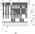
- FIG. 1 shows a cross-sectional view of a semiconductor device, such as a semiconductor memory device 100, according to some embodiments of the disclosure.
- the semiconductor memory device 100 includes two dies that are bonded face to face. Pad structures and connection structures are formed on a back side of one of the two dies using the techniques provided in the present disclosure.
- the semiconductor memory device 100 includes an array die 102 and a CMOS die 101 bonded face to face.
- a semiconductor memory device can include multiple array dies and a CMOS die.
- the multiple array dies and the CMOS die can be stacked and bonded together.
- the CMOS die is respectively coupled to the multiple array dies, and can drive the respective array dies in a similar manner.
- the semiconductor device 100 can be any suitable device.
- the semiconductor device 100 includes at least a first wafer and a second wafer bonded face to face.
- the array die 102 is disposed with other array dies on the first wafer
- the CMOS die 101 is disposed with other CMOS dies on the second wafer.
- the first wafer and the second wafer are bonded together, thus the array dies on the first wafer are bonded with corresponding CMOS dies on the second wafer.
- the semiconductor device 100 is a semiconductor chip with at least the array die 102 and the CMOS die 101 bonded together.
- the semiconductor chip is diced from wafers that are bonded together.
- the semiconductor device 100 is a semiconductor package that includes one or more semiconductor chips assembled on a package substrate.
- the array die 102 includes one or more semiconductor portions 105, and insulating portions 106 between the semiconductor portions 105.
- the memory cell arrays can be formed in the semiconductor portions 105, the insulating portions can isolate the semiconductor portions 105 and provide space for contact structures 170.
- the CMOS die 101 includes a substrate 104, and peripheral circuitry formed on the substrate 104.
- the main surface (of the dies or wafers) is referred to as an X-Y plane, and the direction perpendicular to the main surface is referred to as Z direction.
- connection structures 121 and pad structures 122-123 are formed on a back side of one of the two dies, such as the array die 102.
- the pad structures 122-123 are above the insulating portions 106 and each of the pad structures 122-123 can be conductively connected with one or more of the contact structures 170.
- a connection structure 121 is above a semiconductor portion 105 and is conductively connected to the semiconductor portion 105.
- the semiconductor portion 105 is coupled to an array common source (ACS) for a memory cell array, and the connection structure 121 is disposed over semiconductor portion(s) 105 for a block of memory cell arrays.
- ACS array common source
- connection structure 121 is formed of metal layers of relatively low resistivity, and when the connection structure 121 covers a relatively large portion of the semiconductor portion 105, the connection structure 121 can connect the ACS of the block of the memory cell arrays with very small parasitic resistance.
- the connection structure 121 can include a portion that is configured as a pad structure for ACS to receive ACS signal from an external source.
- the pad structures 122-123 and the connection structure 121 are made of suitable metal material(s), such as aluminum, and the like that can facilitate attachment of bonding wires.
- the pad structures 122-123 include a titanium layer 126 and an aluminum layer 128, and the connection structure 121 includes a titanium silicide layer 127 and the aluminum layer 128.
- the array die 102 initially includes a substrate and semiconductor portions 105 and the insulating portions 106 are formed on the substrate. The substrate is removed before the formation the pad structures 122-123 and the connection structure 121.
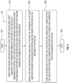
- FIG. 2 shows a flow chart outlining a process 200 for forming a semiconductor memory device, such as the semiconductor memory device 100 according to some embodiments of the disclosure, and FIGs. 3-6 show cross-sectional views of the semiconductor device 100 during the process in accordance with some embodiments.
- the process 200 starts from S201 and proceeds to S210.
- a first die and a second die are bonded face to face.
- the first die includes a first substrate, and includes semiconductor portions and insulating portions disposed on the first substrate on the face side. The insulating portions can insulate the semiconductor portions.
- the first die also includes first transistors formed in the semiconductor portions from the face side of the first die. Further, the first die includes contact structures disposed in the insulating portions that are outside the semiconductor portions. The insulating portions can also insulate the contact structures from each other and from the semiconductor portions.
- the second die includes a second substrate with second transistors formed on a face side of the second die.
- the first die is an array die, such as the array die 102 and the second die is a CMOS die, such as the CMOS die 101.
- the first die can be a CMOS die and the second die can be an array die.
- FIG. 3 shows a cross-sectional view of the semiconductor memory device 100 after a bonding process of two dies.
- the semiconductor memory device 100 includes the array die 102 and the CMOS die 101 that are bonded face to face.
- the array die 102 is fabricated with other array dies on a first wafer, and the CMOS die 101 is fabricated with other CMOS dies on a second wafer.
- the first wafer and the second wafer are fabricated separately.
- memory cell arrays and I/O contact structures are formed on the first wafer using processes that operate on the face side of the first wafer.
- first bonding structures are formed on the face side of the first wafer.
- periphery circuitry is formed on the second wafer using processes that operate on the face side of the second wafer, and second bonding structures are formed on the face side of the second wafer.
- the first wafer and the second wafer can be bonded face to face using a wafer-to-wafer bonding technology.
- the first bonding structures on the first wafer are bonded with corresponding second bonding structures on the second wafer, thus the array dies on the first wafer are respectively bonded with the CMOS dies on the second wafer.
- the array die 102 includes a substrate 103. On the substrate 103, one or more semiconductor portions 105 and insulating portions 106 are formed.
- the insulating portions 106 are formed of insulating material, such as silicon oxide and the like that can insulate the semiconductor portions 105. Further, memory cell arrays can be formed in the semiconductor portions 105 and contact structures can be formed in the insulating portions 106.
- the CMOS die 101 includes a substrate 104, and includes peripheral circuitry formed on the substrate 104.
- the substrate 103 and the substrate 104 respectively can be any suitable substrate, such as a silicon (Si) substrate, a germanium (Ge) substrate, a silicon-germanium (SiGe) substrate, and/or a silicon-on-insulator (SOI) substrate.
- the substrate 103 and the substrate 104 respectively may include a semiconductor material, for example, a Group IV semiconductor, a Group III-V compound semiconductor, or a Group II-VI oxide semiconductor.
- the Group IV semiconductor may include Si, Ge, or SiGe.
- the substrate 103 and the substrate 104 respectively may be a bulk wafer or an epitaxial layer.
- a substrate is formed of multiple layers.
- the substrate 103 includes multiple layers, such as a bulk portion 111, a silicon oxide layer 112 and a silicon nitride layer 113, as shown in FIG. 3 .
- the memory cell arrays are formed on the substrate 103 of the array die 102 and the peripheral circuitry is formed on the substrate 104 of the CMOS die 101.
- the array die 102 and the CMOS die 101 are disposed face to face (the surface with circuitry disposed on is referred to as face, and the opposite surface is referred to as back), and bonded together.
- a semiconductor portion 105 is formed on the substrate 103, and a block of three dimensional (3D) NAND memory cell strings can be formed in the semiconductor portion 105.
- the semiconductor portion 105 is conductively coupled with an array common source of the memory cell strings.
- a memory cell array is formed in a core region 115 as an array of vertical memory cell strings.
- the array die 102 includes a staircase region 116 and an insulating region 117.
- the staircase region 116 is used to facilitate making connections to, for example, gates of the memory cells in the vertical memory cell strings, gates of the select transistors, and the like.
- the gates of the memory cells in the vertical memory cell strings correspond to word lines for the NAND memory architecture.
- the insulating region 117 is used to form the insulating portion 106.
- vertical memory cell strings 180 are shown as representation of an array of vertical memory cell strings formed in the core region 115.
- the vertical memory cell strings 180 are formed in a stack of layers 190.
- the stack of layers 190 includes gate layers 195 and insulating layers 194 that are stacked alternatingly.
- the gate layers 195 and the insulating layers 194 are configured to form transistors that are stacked vertically.
- the stack of transistors includes memory cells and select transistors, such as one or more bottom select transistors, one or more top select transistors and the like.
- the stack of transistors can include one or more dummy select transistors.
- the gate layers 195 correspond to gates of the transistors.
- the gate layers 195 are made of gate stack materials, such as high dielectric constant (high-k) gate insulator layers, metal gate (MG) electrode, and the like.
- the insulating layers 194 are made of insulating material(s), such as silicon nitride, silicon dioxide, and the like.
- the vertical memory cell strings are formed of channel structures 181 that extend vertically (Z direction) into the stack of layers 190.
- the channel structures 181 can be disposed separate from each other in the X-Y plane.
- the channel structures 181 are disposed in the form of arrays between gate line cut structures (not shown).
- the gate line cut structures are used to facilitate replacement of sacrificial layers with the gate layers 195 in a gate-last process.
- the arrays of the channel structures 181 can have any suitable array shape, such as a matrix array shape along the X direction and the Y direction, a zig-zag array shape along the X or Y direction, a beehive (e.g., hexagonal) array shape, and the like.
- each of the channel structures has a circular shape in the X-Y plane, and a pillar shape in the X-Z plane and Y-Z plane.
- the quantity and arrangement of the channel structures between gate line cut structures is not limited.
- the channel structure 181 has a pillar shape that extends in the Z direction that is perpendicular to the direction of the main surface of the substrate 103.
- the channel structure 181 is formed by materials in the circular shape in the X-Y plane, and extends in the Z direction.
- the channel structure 181 includes function layers, such as a blocking insulating layer 182 (e.g., silicon oxide), a charge storage layer (e.g., silicon nitride) 183, a tunneling insulating layer 184 (e.g., silicon oxide), a semiconductor layer 185, and an insulating layer 186 that have the circular shape in the X-Y plane, and extend in the Z direction.
- a blocking insulating layer 182 e.g., silicon oxide
- a charge storage layer e.g., silicon nitride
- a tunneling insulating layer 184 e.g., silicon oxide
- semiconductor layer 185 e.g., silicon oxide
- the blocking insulating layer 182 (e.g., silicon oxide) is formed on the sidewall of a hole (into the stack of layers 190) for the channel structure 181, and then the charge storage layer (e.g., silicon nitride) 183, the tunneling insulating layer 184, the semiconductor layer 185, and the insulating layer 186 are sequentially stacked from the sidewall.
- the semiconductor layer 185 can be any suitable semiconductor material, such as polysilicon or monocrystalline silicon, and the semiconductor material may be un-doped or may include a p-type or n-type dopant. In some examples, the semiconductor material is intrinsic silicon material that is un-doped.
- the insulating layer 186 is formed of an insulating material, such as silicon oxide and/or silicon nitride, and/or may be formed as an air gap.
- the channel structure 181 and the stack of layers 190 together form the memory cell string 180.
- the semiconductor layer 185 corresponds to the channel portions for transistors in the memory cell string 180
- the gate layers 195 corresponds to the gates of the transistors in the memory cells string 180.
- a transistor has a gate that controls a channel, and has a drain and a source at each side of the channel.
- the drain the bottom side of the channel for transistors in FIG. 3
- the upper side of the channel for transistors in FIG. 3 is referred to as the source. It is noted that the drain and the source can be switched under certain driving configurations. In the FIG.
- the semiconductor layer 185 corresponds to connected channels of the transistors.
- the drain of the specific transistor is connected with a source of a lower transistor below the specific transistor, and the source of the specific transistor is connected with a drain of an upper transistor above the specific transistor in the FIG. 3 example.
- the transistors in the memory cell string 180 are connected in series. It is noted that “upper” and “lower” are used specific to FIG. 3 where the array die 102 is disposed upside down.
- the memory cell string 180 includes memory cell transistors (or referred to as memory cells).
- a memory cell transistor can have different threshold voltages based on carrier trappings in a portion of the charge storage layer 183 that corresponds to a floating gate for the memory cell transistor. For example, when a significant amount of holes are trapped (stored) in the floating gate of the memory cell transistor, the threshold voltage of the memory cell transistor is lower than a predefined value, then the memory cell transistor is in a un-programed state (also referred to as erased state) corresponding to logic "1". When holes are expelled from the floating gate, the threshold voltage of the memory cell transistor is above a predefined value, thus the memory cell transistor is in a programed state corresponding to logic "0" in some examples.
- the memory cell string 180 includes one or more top select transistors configured to couple/de-couple the memory cells in the memory cell string 180 to a bit line, and includes one or more bottom select transistors configured to couple/de-couple the memory cells in the memory cell string 180 to the ACS.
- the top select transistors are controlled by top select gates (TSG). For example, when a TSG voltage (voltage applied to the TSG) is larger than a threshold voltage of the top select transistors, the top select transistors in the memory cell string 180 are turned on and the memory cells in the memory cell string 180 are coupled to the bit line (e.g., drain of the string of memory cells is coupled to the bit line); and when the TSG voltage (voltage applied to the TSG) is smaller than the threshold voltage of the top select transistors, the top select transistors are turned off and the memory cells in the memory cell string 180 are de-coupled from the bit line (e.g., drain of the string of memory cells is decoupled from the bit line) .
- TSG top select gates
- the bottom select transistors are controlled by bottom select gates (BSG). For example, when a BSG voltage (voltage applied to the BSG) is larger than a threshold voltage of the bottom select transistors in a memory cell string 180, the bottom select transistors are turned on and the memory cells in the memory cell string 180 are coupled to the ACS (e.g., source of the string of memory cells in the memory cell string 180 is coupled to the ACS); and when the BSG voltage (voltage applied to the BSG) is smaller than the threshold voltage of the bottom select transistors, the bottom select transistors are turned off and the memory cells are de-coupled from the ACS (e.g., source of the string of memory cells in the memory cell string 180 is de-coupled from the ACS).
- BSG voltage voltage applied to the BSG
- the bottom select transistors are turned on and the memory cells in the memory cell string 180 are coupled to the ACS (e.g., source of the string of memory cells in the memory cell string 180 is coupled to the ACS).
- the upper portion of the semiconductor layer 185 in the channel hole corresponds to a source side of the vertical memory cell string 180, and the upper portion is labeled as 185(S).
- a common source layer 189 is formed in conductive connection with the source of the vertical memory cell string 180.
- the common source layer 189 can includes one or more layers.
- the common source layer 189 includes silicon material, such as intrinsic polysilicon, doped polysilicon (such as N-type doped silicon, P-type doped silicon and the like) and the like.
- the common source layer 189 may include metal silicide to improve conductivity.
- the common source layer 189 is similarly in conductive connection with sources of other vertical memory cell strings (not shown) in the semiconductor portion 105, and thus forms an array common source (ACS).
- ACS array common source
- the semiconductor portion 105 and the common source layer 189 are conductively coupled in some examples, thus the semiconductor portion 105 can be configured as the array common source for the vertical memory cell strings formed in the semiconductor portion 105.
- the semiconductor layer 185 extends vertically from the source side of the channel structure 181 down, and forms a bottom portion corresponds to a drain side of the vertical memory cell string 180.
- the bottom portion of the semiconductor layer 185 is labeled as 185(D). It is noted that drain side and the source side are named for the ease of description. The drain side and the source side may function differently from the names.
- interconnection structures such as a via 162, a metal wire 163, a bonding structure 164, and the like, can be formed to electrically couple the bottom portion of the semiconductor layer 185(D) to a bit line (BL).
- the staircase region 116 includes a staircase that is formed to facilitate word line connections to the gates of transistors (e.g., memory cells, top select transistor(s), bottom select transistor(s) and the like).
- a word line connection structure 150 includes a word line contact plug 151, a via structure 152, and metal wire 153 that are conductively coupled together.
- the word line connection structure 150 can electrically couple a WL to a gate terminal of a transistor in the memory cell string 180.
- the contact structures 170 are formed in the insulating region 117.
- the contact structures 170 can be formed at the same time as the word line connection structures 150 by processing on the face side of the array die 102.
- the contact structures 170 have similar structures as the word line connection structures 150.
- a contact structure 170 can include a contact plug 171, a via structure 172, and metal wire 173 that are conductively coupled together.
- a mask that includes patterns for the contact plugs 171 and the word line contact plugs 151 can be used.
- the mask is used to form contact holes for the contact plugs 171 and the word line contact plugs 151.
- Etch process can be used to form the contact holes.
- etching of the contact holes for the word line contact plugs 151 can stop on the gate layers 195 and the etching of the contact holes for the contact plugs 171 can stop in the oxide layer 112.
- the contact holes can be filled with suitable liner layer (e.g., titanium/titanium nitride) and a metal layer (e.g., tungsten) to form the contact plugs, such as the contact plugs 171 and the word line contact plugs 151.
- Further back end of line (BEOL) processes are used to form various connection structures, such via structures, metal wires, bonding structures, and the like.
- bonding structures are respectively formed on the face sides of the array die 102 and the CMOS die 101.
- bonding structures 174 and 164 are formed on face side of the array die 102
- bonding structures 131 and 134 are formed on the face side of the CMOS die 101.
- the array die 102 and the CMOS die 101 are disposed face-to-face (circuitry side is face, and the substrate side is back) and bonded together.
- Corresponding bonding structures on the array die 102 and the CMOS die 101 are aligned and bonded together, and form a bonding interface that conductively couple suitable components on the two dies.
- the bonding structure 164 and the bonding structure 131 are bonded together to couple the drain side of the memory cell string 180 with a bit line (BL).
- the bonding structure 174 and the bonding structure 134 are bonded together to couple a contact structure 170 on the array die 102 with an I/O circuit on the CMOS die 101.
- the first substrate of the first die is removed from the back side of the first die.
- the removal of the first substrate exposes the semiconductor portion and the contact structures 170 on the back side of the first die.
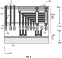
- FIG. 4 shows a cross-sectional view of the semiconductor memory device 100 after the removal of the first substrate 103 from the array die 102.
- the bulk portion 111, the silicon oxide layer 112 and the silicon nitride layer 113 are removed from the back side of the array die 102.
- a first wafer with array dies is bonded with a second wafer with CMOS dies.
- the first substrate is thinned from the back side of the first wafer.
- a chemical mechanical polishing (CMP) process or a grind process is used to remove a majority portion of the bulk portion 111 of the first wafer.
- CMP chemical mechanical polishing
- suitable etch process can be used to remove remaining bulk portion 111, the silicon oxide layer 112 and the silicon nitride layer 113 from the back side of the first wafer.
- the removal of the bulk portion 111, the silicon oxide layer 112 and the silicon nitride layer 113 can reveal the ends (as shown by 175) of the contact structures 170 that protrude from the insulating portions 106.
- the removal of the bulk portion 111, the silicon oxide layer 112 and the silicon nitride layer 113 can also reveal the semiconductor portion 105.
- pad structures and connection structures are formed.
- the pad structures include first pad structures that are conductively connected with the contact structures 170.
- the connection structures are conductively connected with semiconductor portions 150.
- the pad structures and the connection structures are mainly formed of aluminum (Al).
- interfacing layer(s) can be formed between the aluminum and the semiconductor portion 105.
- metal silicide thin films can be used as the interfacing layer(s).
- a metal silicide thin film can be used to enable ohmic contacts between the aluminum and the semiconductor portion 105.
- a metal silicide thin film is used to form local interconnects to the semiconductor portion 105.
- a metal silicide thin film is used as diffusion barriers to prevent aluminum diffusion into the semiconductor portion 105.
- titanium is deposited overall on the back side of the first wafer that is face-to-face bonded with the second wafer, and is then heated in a nitrogen atmosphere.
- the titanium can react with exposed silicon surfaces (such as the semiconductor portion 105) to form titanium silicide.
- the portions e.g., above the insulating portions, above the ends of the contact structures 170 and the like) of titanium which did not react to form silicide.
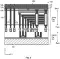
- FIG. 5 shows a cross-sectional view of the semiconductor memory device 100 after the deposition of metal film(s).
- a metal film 120 is deposited on the back side of the first wafer.
- the metal film 120 may have uneven surface due to the protrusion by the ends of the contact structures 170.
- the metal film 120 includes a titanium layer 126 and an aluminum layer 128.
- the titanium layer 126 on the semiconductor portion 105 can react with silicon surface to form titanium silicide 127.
- the titanium layer 126 is deposited and heated in nitrogen atmosphere. Then the aluminum layer 128 is deposited.
- the metal film 120 can be patterned to form pad structures and connection structures.
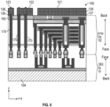
- FIG. 6 shows a cross-sectional view of the semiconductor memory device 100 after the metal film 120 is patterned into pad structures 122-123 and connection structure 121.
- the pad structures 122-123 are respectively connected to the contact structures 170 and are disposed above the insulating portions 106; the connection structure 121 is connected to the semiconductor portion 105.
- a photolithography process is used to define patterns for the pad structures 122-123 and the connection structure 121 into a photoresist layer according to a mask, then an etch process is used to transfer the patterns into the metal film 120 and to from the pad structures 122-123 and the connection structure 121.
- films of the connection structure 121 are directly deposited on the semiconductor portion 105, thus an interface between the connection structure 121 and the semiconductor portion 105 is substantially flat over the semiconductor portion 105.
- the semiconductor portion 105 can be covered by an insulating layer, contact holes are formed in the insulating layer, then suitable metal layers are deposited (into the holes and over the insulating layer) to form contacts and connections.
- the connection structure 121 is formed without using contact holes in insulating layers, and the interface between the connection structure 121 and the semiconductor portion 105 relatively flat, the bottom surface and the top surface of the connection structure 121 on the semiconductor portion 105 are about the same when etch profile related difference is ignored.
- the metal film 120 may have uneven surface.
- the bottom surface of the metal film 120 that interfaces with the insulating portion 106 may have concave portions corresponding to the ends of the contact structures 170, thus the bottom surface of the pad structures 122-123 may have concave portions corresponding to the ends of the contact structures 170.
- the wafer fabrication process can continue further processes, such as, passivation, testing, dicing and the like.
Landscapes
- Semiconductor Memories (AREA)
- Wire Bonding (AREA)
- Internal Circuitry In Semiconductor Integrated Circuit Devices (AREA)
- Non-Volatile Memory (AREA)
- Engineering & Computer Science (AREA)
- Manufacturing & Machinery (AREA)
Abstract
Description
- The present application describes embodiments generally related to semiconductor memory devices.
- Generally, a semiconductor device (e.g., a semiconductor chip) communicates with the outside world through various input/output (I/O) pad structures, such as signaling pad structures, and power/ground (P/G) pad structures and the like. In some examples, a semiconductor chip can include multiple metal layers formed on top of circuitry above a substrate. One or more of the metal layers are used to form pad structures that are conductively coupled with the circuitry above the substrate. The pad structures can be formed to facilitate attachment of bonding wires that can conductively couple the pad structures with external components, such as power supply, ground, other semiconductor chips, metal lines on printed circuit board (PCB) and the like.
- Aspects of the disclosure provide a semiconductor device. The semiconductor device includes a first die and a second die boned face-to-face. The first die includes first transistors formed on a face side of the first die in a semiconductor portion and at least a contact structure disposed in an insulating portion outside the semiconductor portion. The second die includes a substrate and second transistors formed on a face side of the second die. Further, the semiconductor device includes a first pad structure disposed on a back side of the first die and the first pad structure is conductively coupled with the contact structure. An end of the contact structure protrudes from the insulating portion into the first pad structure. Further, in some embodiments, the semiconductor device includes a connection structure disposed on the back side of the first die and conductively connected with the semiconductor portion.
- Especially, the invention is directed to a semiconductor device according to any of claims 1 to 15. The first die and the second die may be boned face-to-face.
- In an embodiment, an interface between the connection structure and the semiconductor portion is substantially flat over the semiconductor portion. In some examples, a bottom surface and a top surface of the connection structure on the semiconductor portion are about a same size.
- In some embodiments, the contact structure includes at least a first metal material that is different from a second metal material in the first pad structure. In an example, the first metal material includes tungsten and the second metal material includes aluminum.
- In some examples, due to the protrusion of the end of the contact structure, a bottom surface of the first pad structure that interfaces with the insulating portion has a concave portion corresponding to the end of the contact structure.
- In some embodiments, the first die includes at least a memory cell array formed in the semiconductor portion, and the second die includes a periphery circuit for the memory cell array. The contact structure on the first die is electrically coupled to an input/output circuit on the second die via bonding structures.
- In some embodiments, the first die includes an input/output circuit that is electrically coupled to the contact structure.
- Aspects of the disclosure provide a method for fabricating a semiconductor device. The method includes bonding a first die and a second die face-to-face. The first die includes a first substrate, first transistors formed in a semiconductor portion on a face side of the first die, and a contact structure disposed in an insulating portion outside the semiconductor portion. The second die includes a second substrate with second transistors formed on a face side of the second. Further, the method includes removing the first substrate from a back side of the first die. The removing of the first substrate exposes an end of the contact structure on the back side of the first die. Then the method includes forming, on the back side of the first die, a first pad structure conductively connected with the contact structure. The end of the contact structure protrudes from the insulating portion inward the first pad structure.
- In some embodiments, the method further includes forming, on the back side of the first die, a connection structure that is conductively connected with the semiconductor portion. In an embodiment, the removing of the first substrate exposes the semiconductor portion from the back side of the first die, and the method includes depositing layers for forming the connection structure. An interface of the layers to the semiconductor portion is substantially flat over the semiconductor portion. In some examples, the method includes patterning the layers to form the connection structure. A bottom surface and a top surface of the connection structure on the semiconductor portion are about a same size.
- In some embodiments, the method includes depositing, on the contact structure that includes at least a first metal material, a second metal material that is different from the first metal material. The first pad structure includes at least the second metal material. The first metal material can be tungsten and the second metal material can be aluminum in an example.
- Aspects of the present disclosure are best understood from the following detailed description when read with the accompanying figures. It is noted that, in accordance with the standard practice in the industry, various features are not drawn to scale. In fact, the dimensions of the various features may be arbitrarily increased or reduced for clarity of discussion.
-
FIG. 1 shows a cross-sectional view of a semiconductor device according to some embodiments of the disclosure. -
FIG. 2 shows a flow chart outlining a process for forming a semiconductor device. -
FIGs. 3-6 show cross-sectional views of a semiconductor device during a fabrication process in accordance with some embodiments. - The following disclosure provides many different embodiments, or examples, for implementing different features of the provided subject matter. Specific examples of components and arrangements are described below to simplify the present disclosure. These are, of course, merely examples and are not intended to be limiting. For example, the formation of a first feature over or on a second feature in the description that follows may include embodiments in which the first and second features are formed in direct contact, and may also include embodiments in which additional features may be formed between the first and second features, such that the first and second features may not be in direct contact. In addition, the present disclosure may repeat reference numerals and/or letters in the various examples. This repetition is for the purpose of simplicity and clarity and does not in itself dictate a relationship between the various embodiments and/or configurations discussed.
- Further, spatially relative terms, such as "beneath," "below," "lower," "above," "upper" and the like, may be used herein for ease of description to describe one element or feature's relationship to another element(s) or feature(s) as illustrated in the figures. The spatially relative terms are intended to encompass different orientations of the device in use or operation in addition to the orientation depicted in the figures. The apparatus may be otherwise oriented (rotated 90 degrees or at other orientations) and the spatially relative descriptors used herein may likewise be interpreted accordingly.
- Aspects of the disclosure provide techniques for forming pad structures for a semiconductor device with two dies (e.g., a first die and a second die) bonded face-to-face. The pad structures are formed on a back side of one of the two dies, such as the first die. The techniques to form the pad structures do not need to form through silicon contacts (TSC) from the back side of the first die and simplify the processes to form the pad structures. In some embodiments, circuit components are formed on the face sides of the two dies. Additionally, at least a contact structure is formed in an insulating portion of the first die from the face side of the first die, and the contact structure is connected to an input/output (I/O) circuit. One of the pad structures on the back side of the first die, such as a first pad structure, is conductively coupled with the contact structure, and the contact structure includes an end that protrudes from the insulating portion inward the first pad structure. In some examples, the first die includes a semiconductor portion with transistors formed in the semiconductor portion. In some embodiments, a connection structure is formed with the pad structures, and is conductively coupled with the semiconductor portion. In an example, the connection structure is conductively coupled with the semiconductor portion without forming contact hole based contacts from the back side of the first die. The pad structures and the connection structure can be formed using same metal layer(s) in some examples.
- According to some aspects of the disclosure, the semiconductor device can be a semiconductor memory device in which one of the two dies includes a memory cell array formed on the face side and is referred to as an array die and the other of the two dies includes periphery circuitry formed on the face side and is referred to as periphery die. In some examples, the periphery circuitry is formed using complementary metal-oxide-semiconductor (CMOS) technology, and the periphery die is also referred to as CMOS die. The pad structures and the connection structure can be formed on the back of the array die or can be formed on the back of the periphery die.
- In some embodiments, the pad structures and the connection structure are formed on the back side of the array die. The array die includes a memory cell array formed in the semiconductor portion. Then, in an example, the connection structure that is conductively coupled with the semiconductor portion can be configured to provide a connection for an array common source (ACS) of the memory cell array.
- According to some aspects of the disclosure, the two dies (e.g., the array die and the periphery die) are formed separately on two wafers. In some embodiments, a first wafer that includes array dies and a second wafer that includes periphery dies are formed separately. For example, the first wafer can be fabricated to optimize density and performance of the memory cell arrays without compromising to fabrication limitations due to the periphery circuitry; and the second wafer can be fabricated to optimize the performance of the periphery circuitry without compromising to fabrication limitations due to the memory cell array. In some embodiments, the first wafer and the second wafer can be bonded face to face using a wafer-to-wafer bonding technology, thus the array dies on the first wafer are respectively bonded with periphery dies on the second wafer. Then, the techniques provided in the present disclosure can be used to fabricate pad structures on a back side of one of the two wafers.
-
FIG. 1 shows a cross-sectional view of a semiconductor device, such as asemiconductor memory device 100, according to some embodiments of the disclosure. Thesemiconductor memory device 100 includes two dies that are bonded face to face. Pad structures and connection structures are formed on a back side of one of the two dies using the techniques provided in the present disclosure. - Specifically, in the
FIG. 1 example, thesemiconductor memory device 100 includes an array die 102 and a CMOS die 101 bonded face to face. It is noted that, in some embodiments, a semiconductor memory device can include multiple array dies and a CMOS die. The multiple array dies and the CMOS die can be stacked and bonded together. The CMOS die is respectively coupled to the multiple array dies, and can drive the respective array dies in a similar manner. - The
semiconductor device 100 can be any suitable device. In some examples, thesemiconductor device 100 includes at least a first wafer and a second wafer bonded face to face. The array die 102 is disposed with other array dies on the first wafer, and the CMOS die 101 is disposed with other CMOS dies on the second wafer. The first wafer and the second wafer are bonded together, thus the array dies on the first wafer are bonded with corresponding CMOS dies on the second wafer. In some examples, thesemiconductor device 100 is a semiconductor chip with at least the array die 102 and the CMOS die 101 bonded together. In an example, the semiconductor chip is diced from wafers that are bonded together. In another example, thesemiconductor device 100 is a semiconductor package that includes one or more semiconductor chips assembled on a package substrate. - The array die 102 includes one or
more semiconductor portions 105, and insulatingportions 106 between thesemiconductor portions 105. The memory cell arrays can be formed in thesemiconductor portions 105, the insulating portions can isolate thesemiconductor portions 105 and provide space forcontact structures 170. The CMOS die 101 includes asubstrate 104, and peripheral circuitry formed on thesubstrate 104. For simplicity, the main surface (of the dies or wafers) is referred to as an X-Y plane, and the direction perpendicular to the main surface is referred to as Z direction. - Further, in the
FIG. 1 example,connection structures 121 and pad structures 122-123 are formed on a back side of one of the two dies, such as the array die 102. Specifically, in theFIG. 1 example, the pad structures 122-123 are above the insulatingportions 106 and each of the pad structures 122-123 can be conductively connected with one or more of thecontact structures 170. In theFIG. 1 example, aconnection structure 121 is above asemiconductor portion 105 and is conductively connected to thesemiconductor portion 105. In some examples, thesemiconductor portion 105 is coupled to an array common source (ACS) for a memory cell array, and theconnection structure 121 is disposed over semiconductor portion(s) 105 for a block of memory cell arrays. In some example, theconnection structure 121 is formed of metal layers of relatively low resistivity, and when theconnection structure 121 covers a relatively large portion of thesemiconductor portion 105, theconnection structure 121 can connect the ACS of the block of the memory cell arrays with very small parasitic resistance. Theconnection structure 121 can include a portion that is configured as a pad structure for ACS to receive ACS signal from an external source. The pad structures 122-123 and theconnection structure 121 are made of suitable metal material(s), such as aluminum, and the like that can facilitate attachment of bonding wires. In some examples, the pad structures 122-123 include atitanium layer 126 and analuminum layer 128, and theconnection structure 121 includes atitanium silicide layer 127 and thealuminum layer 128. - It is noted that, for ease of illustration, some components of the
semiconductor memory device 100, such as passivation structures, and the like are not shown. - It is noted that the array die 102 initially includes a substrate and
semiconductor portions 105 and the insulatingportions 106 are formed on the substrate. The substrate is removed before the formation the pad structures 122-123 and theconnection structure 121. -
FIG. 2 shows a flow chart outlining aprocess 200 for forming a semiconductor memory device, such as thesemiconductor memory device 100 according to some embodiments of the disclosure, andFIGs. 3-6 show cross-sectional views of thesemiconductor device 100 during the process in accordance with some embodiments. Theprocess 200 starts from S201 and proceeds to S210. - At S210, a first die and a second die are bonded face to face. The first die includes a first substrate, and includes semiconductor portions and insulating portions disposed on the first substrate on the face side. The insulating portions can insulate the semiconductor portions. The first die also includes first transistors formed in the semiconductor portions from the face side of the first die. Further, the first die includes contact structures disposed in the insulating portions that are outside the semiconductor portions. The insulating portions can also insulate the contact structures from each other and from the semiconductor portions. The second die includes a second substrate with second transistors formed on a face side of the second die.
- In some embodiments, the first die is an array die, such as the array die 102 and the second die is a CMOS die, such as the CMOS die 101. In some examples, the first die can be a CMOS die and the second die can be an array die.
-
FIG. 3 shows a cross-sectional view of thesemiconductor memory device 100 after a bonding process of two dies. Thesemiconductor memory device 100 includes the array die 102 and the CMOS die 101 that are bonded face to face. - In some embodiments, the array die 102 is fabricated with other array dies on a first wafer, and the CMOS die 101 is fabricated with other CMOS dies on a second wafer. In some examples, the first wafer and the second wafer are fabricated separately. For examples, memory cell arrays and I/O contact structures are formed on the first wafer using processes that operate on the face side of the first wafer. Further, first bonding structures are formed on the face side of the first wafer. Similarly, periphery circuitry is formed on the second wafer using processes that operate on the face side of the second wafer, and second bonding structures are formed on the face side of the second wafer.
- In some embodiments, the first wafer and the second wafer can be bonded face to face using a wafer-to-wafer bonding technology. The first bonding structures on the first wafer are bonded with corresponding second bonding structures on the second wafer, thus the array dies on the first wafer are respectively bonded with the CMOS dies on the second wafer.
- The array die 102 includes a
substrate 103. On thesubstrate 103, one ormore semiconductor portions 105 and insulatingportions 106 are formed. The insulatingportions 106 are formed of insulating material, such as silicon oxide and the like that can insulate thesemiconductor portions 105. Further, memory cell arrays can be formed in thesemiconductor portions 105 and contact structures can be formed in the insulatingportions 106. The CMOS die 101 includes asubstrate 104, and includes peripheral circuitry formed on thesubstrate 104. - The
substrate 103 and thesubstrate 104 respectively can be any suitable substrate, such as a silicon (Si) substrate, a germanium (Ge) substrate, a silicon-germanium (SiGe) substrate, and/or a silicon-on-insulator (SOI) substrate. Thesubstrate 103 and thesubstrate 104 respectively may include a semiconductor material, for example, a Group IV semiconductor, a Group III-V compound semiconductor, or a Group II-VI oxide semiconductor. The Group IV semiconductor may include Si, Ge, or SiGe. Thesubstrate 103 and thesubstrate 104 respectively may be a bulk wafer or an epitaxial layer. In some examples, a substrate is formed of multiple layers. For example, thesubstrate 103 includes multiple layers, such as abulk portion 111, asilicon oxide layer 112 and asilicon nitride layer 113, as shown inFIG. 3 . - In the
FIG. 3 example, the memory cell arrays are formed on thesubstrate 103 of the array die 102 and the peripheral circuitry is formed on thesubstrate 104 of the CMOS die 101. The array die 102 and the CMOS die 101 are disposed face to face (the surface with circuitry disposed on is referred to as face, and the opposite surface is referred to as back), and bonded together. - In some examples, a
semiconductor portion 105 is formed on thesubstrate 103, and a block of three dimensional (3D) NAND memory cell strings can be formed in thesemiconductor portion 105. Thesemiconductor portion 105 is conductively coupled with an array common source of the memory cell strings. In some examples, a memory cell array is formed in acore region 115 as an array of vertical memory cell strings. Besides thecore region 115, the array die 102 includes astaircase region 116 and aninsulating region 117. Thestaircase region 116 is used to facilitate making connections to, for example, gates of the memory cells in the vertical memory cell strings, gates of the select transistors, and the like. The gates of the memory cells in the vertical memory cell strings correspond to word lines for the NAND memory architecture. Theinsulating region 117 is used to form the insulatingportion 106. - In the
FIG. 3 example, vertical memory cell strings 180 are shown as representation of an array of vertical memory cell strings formed in thecore region 115. The vertical memory cell strings 180 are formed in a stack oflayers 190. The stack oflayers 190 includes gate layers 195 and insulatinglayers 194 that are stacked alternatingly. The gate layers 195 and the insulatinglayers 194 are configured to form transistors that are stacked vertically. In some examples, the stack of transistors includes memory cells and select transistors, such as one or more bottom select transistors, one or more top select transistors and the like. In some examples, the stack of transistors can include one or more dummy select transistors. The gate layers 195 correspond to gates of the transistors. The gate layers 195 are made of gate stack materials, such as high dielectric constant (high-k) gate insulator layers, metal gate (MG) electrode, and the like. The insulatinglayers 194 are made of insulating material(s), such as silicon nitride, silicon dioxide, and the like. - According to some aspects of the disclosure, the vertical memory cell strings are formed of
channel structures 181 that extend vertically (Z direction) into the stack oflayers 190. Thechannel structures 181 can be disposed separate from each other in the X-Y plane. In some embodiments, thechannel structures 181 are disposed in the form of arrays between gate line cut structures (not shown). The gate line cut structures are used to facilitate replacement of sacrificial layers with the gate layers 195 in a gate-last process. The arrays of thechannel structures 181 can have any suitable array shape, such as a matrix array shape along the X direction and the Y direction, a zig-zag array shape along the X or Y direction, a beehive (e.g., hexagonal) array shape, and the like. In some embodiments, each of the channel structures has a circular shape in the X-Y plane, and a pillar shape in the X-Z plane and Y-Z plane. In some embodiments, the quantity and arrangement of the channel structures between gate line cut structures is not limited. - In some embodiments, the
channel structure 181 has a pillar shape that extends in the Z direction that is perpendicular to the direction of the main surface of thesubstrate 103. In an embodiment, thechannel structure 181 is formed by materials in the circular shape in the X-Y plane, and extends in the Z direction. For example, thechannel structure 181 includes function layers, such as a blocking insulating layer 182 (e.g., silicon oxide), a charge storage layer (e.g., silicon nitride) 183, a tunneling insulating layer 184 (e.g., silicon oxide), asemiconductor layer 185, and an insulatinglayer 186 that have the circular shape in the X-Y plane, and extend in the Z direction. In an example, the blocking insulating layer 182 (e.g., silicon oxide) is formed on the sidewall of a hole (into the stack of layers 190) for thechannel structure 181, and then the charge storage layer (e.g., silicon nitride) 183, the tunneling insulatinglayer 184, thesemiconductor layer 185, and the insulatinglayer 186 are sequentially stacked from the sidewall. Thesemiconductor layer 185 can be any suitable semiconductor material, such as polysilicon or monocrystalline silicon, and the semiconductor material may be un-doped or may include a p-type or n-type dopant. In some examples, the semiconductor material is intrinsic silicon material that is un-doped. However due to defects, intrinsic silicon material can have a carrier density in the order of 1010 cm-3 in some examples. The insulatinglayer 186 is formed of an insulating material, such as silicon oxide and/or silicon nitride, and/or may be formed as an air gap. - According to some aspects of the disclosure, the
channel structure 181 and the stack oflayers 190 together form thememory cell string 180. For example, thesemiconductor layer 185 corresponds to the channel portions for transistors in thememory cell string 180, and the gate layers 195 corresponds to the gates of the transistors in thememory cells string 180. Generally, a transistor has a gate that controls a channel, and has a drain and a source at each side of the channel. For simplicity, in theFIG. 3 example, the bottom side of the channel for transistors inFIG. 3 is referred to as the drain, and the upper side of the channel for transistors inFIG. 3 is referred to as the source. It is noted that the drain and the source can be switched under certain driving configurations. In theFIG. 3 example, thesemiconductor layer 185 corresponds to connected channels of the transistors. For a specific transistor, the drain of the specific transistor is connected with a source of a lower transistor below the specific transistor, and the source of the specific transistor is connected with a drain of an upper transistor above the specific transistor in theFIG. 3 example. Thus, the transistors in thememory cell string 180 are connected in series. It is noted that "upper" and "lower" are used specific toFIG. 3 where the array die 102 is disposed upside down. - The
memory cell string 180 includes memory cell transistors (or referred to as memory cells). A memory cell transistor can have different threshold voltages based on carrier trappings in a portion of thecharge storage layer 183 that corresponds to a floating gate for the memory cell transistor. For example, when a significant amount of holes are trapped (stored) in the floating gate of the memory cell transistor, the threshold voltage of the memory cell transistor is lower than a predefined value, then the memory cell transistor is in a un-programed state (also referred to as erased state) corresponding to logic "1". When holes are expelled from the floating gate, the threshold voltage of the memory cell transistor is above a predefined value, thus the memory cell transistor is in a programed state corresponding to logic "0" in some examples. - The
memory cell string 180 includes one or more top select transistors configured to couple/de-couple the memory cells in thememory cell string 180 to a bit line, and includes one or more bottom select transistors configured to couple/de-couple the memory cells in thememory cell string 180 to the ACS. - The top select transistors are controlled by top select gates (TSG). For example, when a TSG voltage (voltage applied to the TSG) is larger than a threshold voltage of the top select transistors, the top select transistors in the
memory cell string 180 are turned on and the memory cells in thememory cell string 180 are coupled to the bit line (e.g., drain of the string of memory cells is coupled to the bit line); and when the TSG voltage (voltage applied to the TSG) is smaller than the threshold voltage of the top select transistors, the top select transistors are turned off and the memory cells in thememory cell string 180 are de-coupled from the bit line (e.g., drain of the string of memory cells is decoupled from the bit line) . - Similarly, the bottom select transistors are controlled by bottom select gates (BSG). For example, when a BSG voltage (voltage applied to the BSG) is larger than a threshold voltage of the bottom select transistors in a
memory cell string 180, the bottom select transistors are turned on and the memory cells in thememory cell string 180 are coupled to the ACS (e.g., source of the string of memory cells in thememory cell string 180 is coupled to the ACS); and when the BSG voltage (voltage applied to the BSG) is smaller than the threshold voltage of the bottom select transistors, the bottom select transistors are turned off and the memory cells are de-coupled from the ACS (e.g., source of the string of memory cells in thememory cell string 180 is de-coupled from the ACS). - Shown in
FIG. 3 , the upper portion of thesemiconductor layer 185 in the channel hole corresponds to a source side of the verticalmemory cell string 180, and the upper portion is labeled as 185(S). In theFIG. 3 example, acommon source layer 189 is formed in conductive connection with the source of the verticalmemory cell string 180. Thecommon source layer 189 can includes one or more layers. In some examples, thecommon source layer 189 includes silicon material, such as intrinsic polysilicon, doped polysilicon (such as N-type doped silicon, P-type doped silicon and the like) and the like. In some examples, thecommon source layer 189 may include metal silicide to improve conductivity. Thecommon source layer 189 is similarly in conductive connection with sources of other vertical memory cell strings (not shown) in thesemiconductor portion 105, and thus forms an array common source (ACS). - According to some aspects of the disclosure, the
semiconductor portion 105 and thecommon source layer 189 are conductively coupled in some examples, thus thesemiconductor portion 105 can be configured as the array common source for the vertical memory cell strings formed in thesemiconductor portion 105. - In the
FIG. 3 example, in thechannel structure 181, thesemiconductor layer 185 extends vertically from the source side of thechannel structure 181 down, and forms a bottom portion corresponds to a drain side of the verticalmemory cell string 180. The bottom portion of thesemiconductor layer 185 is labeled as 185(D). It is noted that drain side and the source side are named for the ease of description. The drain side and the source side may function differently from the names. - In the
FIG. 3 example, interconnection structures, such as a via 162, ametal wire 163, abonding structure 164, and the like, can be formed to electrically couple the bottom portion of the semiconductor layer 185(D) to a bit line (BL). - Further in
FIG. 3 example, thestaircase region 116 includes a staircase that is formed to facilitate word line connections to the gates of transistors (e.g., memory cells, top select transistor(s), bottom select transistor(s) and the like). For example, a wordline connection structure 150 includes a wordline contact plug 151, a viastructure 152, andmetal wire 153 that are conductively coupled together. The wordline connection structure 150 can electrically couple a WL to a gate terminal of a transistor in thememory cell string 180. - In the
FIG. 3 example, thecontact structures 170 are formed in theinsulating region 117. In some embodiments, thecontact structures 170 can be formed at the same time as the wordline connection structures 150 by processing on the face side of the array die 102. Thus, in some examples, thecontact structures 170 have similar structures as the wordline connection structures 150. Specifically, acontact structure 170 can include acontact plug 171, a viastructure 172, andmetal wire 173 that are conductively coupled together. - In some examples, a mask that includes patterns for the contact plugs 171 and the word line contact plugs 151 can be used. The mask is used to form contact holes for the contact plugs 171 and the word line contact plugs 151. Etch process can be used to form the contact holes. In an example, etching of the contact holes for the word line contact plugs 151 can stop on the gate layers 195 and the etching of the contact holes for the contact plugs 171 can stop in the
oxide layer 112. Further, the contact holes can be filled with suitable liner layer (e.g., titanium/titanium nitride) and a metal layer (e.g., tungsten) to form the contact plugs, such as the contact plugs 171 and the word line contact plugs 151. Further back end of line (BEOL) processes are used to form various connection structures, such via structures, metal wires, bonding structures, and the like. - Further, in the
FIG. 3 examples, bonding structures are respectively formed on the face sides of the array die 102 and the CMOS die 101. For example,bonding structures bonding structures - In the
FIG. 3 example, the array die 102 and the CMOS die 101 are disposed face-to-face (circuitry side is face, and the substrate side is back) and bonded together. Corresponding bonding structures on the array die 102 and the CMOS die 101 are aligned and bonded together, and form a bonding interface that conductively couple suitable components on the two dies. For example, thebonding structure 164 and thebonding structure 131 are bonded together to couple the drain side of thememory cell string 180 with a bit line (BL). In another example, thebonding structure 174 and thebonding structure 134 are bonded together to couple acontact structure 170 on the array die 102 with an I/O circuit on the CMOS die 101. - Referring back to S220, the first substrate of the first die is removed from the back side of the first die. The removal of the first substrate exposes the semiconductor portion and the
contact structures 170 on the back side of the first die. -
FIG. 4 shows a cross-sectional view of thesemiconductor memory device 100 after the removal of thefirst substrate 103 from the array die 102. In theFIG. 4 example, thebulk portion 111, thesilicon oxide layer 112 and thesilicon nitride layer 113 are removed from the back side of the array die 102. In some examples, after a wafer-to-wafer bonding process, a first wafer with array dies is bonded with a second wafer with CMOS dies. Then, the first substrate is thinned from the back side of the first wafer. In an example, a chemical mechanical polishing (CMP) process or a grind process is used to remove a majority portion of thebulk portion 111 of the first wafer. Further, suitable etch process can be used to remove remainingbulk portion 111, thesilicon oxide layer 112 and thesilicon nitride layer 113 from the back side of the first wafer. The removal of thebulk portion 111, thesilicon oxide layer 112 and thesilicon nitride layer 113 can reveal the ends (as shown by 175) of thecontact structures 170 that protrude from the insulatingportions 106. The removal of thebulk portion 111, thesilicon oxide layer 112 and thesilicon nitride layer 113 can also reveal thesemiconductor portion 105. - Referring back to
FIG. 2 , at S230, at the back side of the first die, pad structures and connection structures are formed. In some embodiments, the pad structures include first pad structures that are conductively connected with thecontact structures 170. The connection structures are conductively connected withsemiconductor portions 150. - In some embodiments, the pad structures and the connection structures are mainly formed of aluminum (Al). In some embodiments, interfacing layer(s) can be formed between the aluminum and the
semiconductor portion 105. In some examples, metal silicide thin films can be used as the interfacing layer(s). In an example, a metal silicide thin film can be used to enable ohmic contacts between the aluminum and thesemiconductor portion 105. In another example, a metal silicide thin film is used to form local interconnects to thesemiconductor portion 105. In another example, a metal silicide thin film is used as diffusion barriers to prevent aluminum diffusion into thesemiconductor portion 105. - In some examples, titanium is deposited overall on the back side of the first wafer that is face-to-face bonded with the second wafer, and is then heated in a nitrogen atmosphere. The titanium can react with exposed silicon surfaces (such as the semiconductor portion 105) to form titanium silicide. The portions (e.g., above the insulating portions, above the ends of the
contact structures 170 and the like) of titanium which did not react to form silicide. - Then, metal film(s) can be formed on the surface of the back side of the first wafer.
FIG. 5 shows a cross-sectional view of thesemiconductor memory device 100 after the deposition of metal film(s). In theFIG. 5 example, ametal film 120 is deposited on the back side of the first wafer. Themetal film 120 may have uneven surface due to the protrusion by the ends of thecontact structures 170. In some embodiments, themetal film 120 includes atitanium layer 126 and analuminum layer 128. In an embodiment, thetitanium layer 126 on thesemiconductor portion 105 can react with silicon surface to formtitanium silicide 127. For example, thetitanium layer 126 is deposited and heated in nitrogen atmosphere. Then thealuminum layer 128 is deposited. - The
metal film 120 can be patterned to form pad structures and connection structures.FIG. 6 shows a cross-sectional view of thesemiconductor memory device 100 after themetal film 120 is patterned into pad structures 122-123 andconnection structure 121. In theFIG. 6 example, the pad structures 122-123 are respectively connected to thecontact structures 170 and are disposed above the insulatingportions 106; theconnection structure 121 is connected to thesemiconductor portion 105. In some embodiments, a photolithography process is used to define patterns for the pad structures 122-123 and theconnection structure 121 into a photoresist layer according to a mask, then an etch process is used to transfer the patterns into themetal film 120 and to from the pad structures 122-123 and theconnection structure 121. - According to an aspect of the disclosure, films of the
connection structure 121 are directly deposited on thesemiconductor portion 105, thus an interface between theconnection structure 121 and thesemiconductor portion 105 is substantially flat over thesemiconductor portion 105. In a related example, thesemiconductor portion 105 can be covered by an insulating layer, contact holes are formed in the insulating layer, then suitable metal layers are deposited (into the holes and over the insulating layer) to form contacts and connections. Comparing to the related example, theconnection structure 121 is formed without using contact holes in insulating layers, and the interface between theconnection structure 121 and thesemiconductor portion 105 relatively flat, the bottom surface and the top surface of theconnection structure 121 on thesemiconductor portion 105 are about the same when etch profile related difference is ignored. - According to another aspect of the disclosure, due to the protrusion of the ends of the
contact structures 170, themetal film 120 may have uneven surface. For example, the bottom surface of themetal film 120 that interfaces with the insulatingportion 106 may have concave portions corresponding to the ends of thecontact structures 170, thus the bottom surface of the pad structures 122-123 may have concave portions corresponding to the ends of thecontact structures 170. - The wafer fabrication process can continue further processes, such as, passivation, testing, dicing and the like.
- The foregoing outlines features of several embodiments so that those skilled in the art may better understand the aspects of the present disclosure. Those skilled in the art should appreciate that they may readily use the present disclosure as a basis for designing or modifying other processes and structures for carrying out the same purposes and/or achieving the same advantages of the embodiments introduced herein. Those skilled in the art should also realize that such equivalent constructions do not depart from the spirit and scope of the present disclosure, and that they may make various changes, substitutions, and alterations herein without departing from the spirit and scope of the present disclosure.
- In general, the present application also covers the following matters, wherein the following matters also are disclosed in combination with the subject matter of the appended claims. Furthermore, the following matters also are disclosed in combination with the features of the above-described embodiments, independent from one another or in combination with one another:
- 1. A semiconductor device, comprising:
- a first die and a second die boned face-to-face, the first die comprising first transistors formed on a face side of the first die in a semiconductor portion and at least a contact structure disposed in an insulating portion outside the semiconductor portion, the second die comprising a substrate and second transistors formed on a face side of the second die; and
- a first pad structure disposed on a back side of the first die and conductively coupled with the contact structure, an end of the contact structure protruding from the insulating portion into the first pad structure.
- 2. The semiconductor device of matter 1, further comprising:
a connection structure disposed on the back side of the first die and conductively connected with the semiconductor portion. - 3. The semiconductor device of matter 2, wherein an interface between the connection structure and the semiconductor portion is substantially flat over the semiconductor portion.
- 4. The semiconductor device of matters 2 or 3, wherein a bottom surface and a top surface of the connection structure on the semiconductor portion are about a same size.
- 5. The semiconductor device of matters 1 to 4, wherein the contact structure includes at least a first metal material that is different from a second metal material in the first pad structure.
- 6. The semiconductor device of matter 5, wherein the first metal material comprises tungsten and the second metal material comprises aluminum.
- 7. The semiconductor device of matters 1 to 6, wherein a bottom surface of the first pad structure that interfaces with the insulating portion has a concave portion corresponding to the end of the contact structure.
- 8. The semiconductor device of matters 1 to 7, wherein the first die comprises at least a memory cell array formed in the semiconductor portion, the second die comprises a periphery circuit for the memory cell array.
- 9. The semiconductor device of matter 8, wherein the contact structure on the first die is electrically coupled to an input/output circuit on the second die via bonding structures.
- 10. The semiconductor device of matters 1 to 9, wherein the first die comprises an input/output circuit that is electrically coupled to the contact structure.
- 11. A method for fabricating a semiconductor device, especially a semiconductor device of matters 1 to 10, comprising:
- bonding a first die and a second die face-to-face, the first die comprising a first substrate, first transistors formed in a semiconductor portion on a face side of the first substrate, and a contact structure disposed in an insulating portion outside the semiconductor portion, the second die comprising a second substrate with second transistors formed on a face side of the second substrate
- removing the first substrate from a back side of the first die, the removing of the first substrate exposing an end of the contact structure on the back side of the first die; and
- forming, on the back side of the first die, a first pad structure conductively connected with the contact structure, the end of the contact structure protruding from the insulating portion inward the first pad structure.
- 12. The method of matter 11, further comprising:
forming, on the back side of the first die, a connection structure that is conductively connected with the semiconductor portion. - 13. The method of matter 12, wherein the removing of the first substrate exposes the semiconductor portion from the back side of the first die, and the method comprises:
depositing layers for forming the connection structure, an interface of the layers to the semiconductor portion being substantially flat over the semiconductor portion. - 14. The method of matter 13, further comprising:
patterning the layers to form the connection structure with a bottom surface and a top surface of the connection structure on the semiconductor portion being about a same size. - 15. The method of matters 11 to 14, wherein further comprising:
depositing, on the contact structure that comprises at least a first metal material, a second metal material that is different from the first metal material, the first pad structure comprising at least the second metal material. - 16. The method of matter 15, wherein the first metal material comprises tungsten and the second metal material comprises aluminum.
- 17. The method of matters 11 to 16, wherein forming the first pad structure further comprises:
depositing one or more layers for forming the first pad structure on the insulating portion with the end of the contact structure protruding from the insulating portion, a bottom surface of the one or more layers that interfaces with the insulating portion having a concave portion corresponding to the end of the contact structure. - 18. The method of matters 11 to 17, wherein the first die comprises at least a memory cell array formed in the semiconductor portion, the second die comprises a periphery circuit for the memory cell array.
- 19. The method of matter 18, wherein bonding the first die and the second die face-to-face further comprises:
bonding a first bonding structure on the first die with a second bonding structure on the second die, the first bonding structure being conductively coupled with the contact structure on the first die and the second bonding structure being conductively coupled with an input/output circuit on the second die. - 20. The method of matters 11 to 19, wherein the first die comprises an input/output circuit that is electrically coupled to the contact structure.
Claims (15)
- A semiconductor device, comprising:a first die and a second die, the first die comprising first transistors formed on a face side corresponding to a semiconductor portion (105) of the first die and at least two contact structures (170) disposed in an insulating portion (106) outside the semiconductor portion (105), the second die comprising a substrate (103/104) and second transistors formed on a face side of the second die;a first pad structure (122/123) disposed on a back side of the first die and coupled with the at least two contact structures (170), an end of the contact structures (170) protruding from the insulating portion (106) into the first pad structure (122/123); anda connection structure (121) disposed on the back side of the first die above the semiconductor portion (105) and connected with the semiconductor portion (105).
- The semiconductor device of claim 1, wherein:an interface between the connection structure (121) and the semiconductorportion (105) is substantially flat over the semiconductor portion (105).
- The semiconductor device of claim 1 or 2, wherein the contact structures (170) include at least a first metal material that is different from a second metal material in the first pad structure (122/123).
- The semiconductor device of claim 3, wherein the first metal material comprises tungsten and the second metal material comprises aluminum.
- The semiconductor device of any of claims 1 to 4, wherein a bottom surface of the first pad structure (122/123) that interfaces with the insulating portion (106) has a concave portion corresponding to the end of the contact structures (170).
- The semiconductor device of any of claims 1 to 5, wherein the first die comprises at least a memory cell array, the second die comprises a periphery circuit for the memory cell array.
- The semiconductor device of claim 6, wherein one of the contact structures (170) on the first die is coupled to an input/output circuit on the second die via bonding structures.
- The semiconductor device of any of claims 1 to 7, wherein the at least two contact structures (170) connected to a same first pad structure (122/123) are arranged in a row.
- The semiconductor device of any of claims 1 to 8, wherein the first die further comprises a common source layer (189) coupled to the semiconductor portion (105).
- The semiconductor device of claim 9, wherein the common source layer (189) comprises multiple layers.
- The semiconductor device of claim 9, wherein the first die further comprises a stack of layers (190) comprising gate layers (195) and insulating layers (194) that are stacked alternatingly, the stack of layers (190) is located on a side of the common source layer (189) away from the semiconductor portion (105).
- The semiconductor device of claim 11, wherein the first die further comprises a word line connection structure (150) coupled to the gate layers (195).
- The semiconductor device of any of claims 1 to 12, wherein the first pad structure (122/123) comprises a titanium layer.
- A semiconductor device, especially of any claims 1 to 13, com pri sing:a first die and a second die, the first die comprising a semiconductor portion (105), a common source layer (189) coupled to the semiconductor portion (105), first transistors formed on a face side corresponding to the semiconductor portion (105) of the first die and at least two contact structures (170) disposed in an insulating portion (106) outside the semiconductor portion (105), the second die comprising a substrate (103/104) and second transistors formed on a face side of the second die;a first pad structure (122/123) disposed on a back side of the first die and coupled with the at least two contact structures (170), an end of the at least two contact structures (170) protruding from the insulating portion (106) into a same first pad structure (122/123); anda connection structure (121) disposed on the back side of the first die above the semiconductor portion (105) and connected with the semiconductor portion (105).
- The semiconductor device of claim 14, wherein an interface between the connection structure (121) and the semiconductor portion (105) is substantially flat over the semiconductor portion (105).
Priority Applications (1)
| Application Number | Priority Date | Filing Date | Title |
|---|---|---|---|
| EP24203225.8A EP4462483A3 (en) | 2020-09-02 | 2020-09-02 | Pad structures for semiconductor devices |
Applications Claiming Priority (3)
| Application Number | Priority Date | Filing Date | Title |
|---|---|---|---|
| PCT/CN2020/112978 WO2022047648A1 (en) | 2020-09-02 | 2020-09-02 | Pad structures for semiconductor devices |
| EP24203225.8A EP4462483A3 (en) | 2020-09-02 | 2020-09-02 | Pad structures for semiconductor devices |
| EP20951896.8A EP4139958B1 (en) | 2020-09-02 | 2020-09-02 | Pad structures for semiconductor devices |
Related Parent Applications (2)
| Application Number | Title | Priority Date | Filing Date |
|---|---|---|---|
| EP20951896.8A Division-Into EP4139958B1 (en) | 2020-09-02 | 2020-09-02 | Pad structures for semiconductor devices |
| EP20951896.8A Division EP4139958B1 (en) | 2020-09-02 | 2020-09-02 | Pad structures for semiconductor devices |
Publications (2)
| Publication Number | Publication Date |
|---|---|
| EP4462483A2 true EP4462483A2 (en) | 2024-11-13 |
| EP4462483A3 EP4462483A3 (en) | 2025-02-19 |
Family
ID=74033785
Family Applications (2)
| Application Number | Title | Priority Date | Filing Date |
|---|---|---|---|
| EP24203225.8A Pending EP4462483A3 (en) | 2020-09-02 | 2020-09-02 | Pad structures for semiconductor devices |
| EP20951896.8A Active EP4139958B1 (en) | 2020-09-02 | 2020-09-02 | Pad structures for semiconductor devices |
Family Applications After (1)
| Application Number | Title | Priority Date | Filing Date |
|---|---|---|---|
| EP20951896.8A Active EP4139958B1 (en) | 2020-09-02 | 2020-09-02 | Pad structures for semiconductor devices |
Country Status (7)
| Country | Link |
|---|---|
| US (1) | US11424221B2 (en) |
| EP (2) | EP4462483A3 (en) |
| JP (2) | JP7547514B2 (en) |
| KR (2) | KR102934125B1 (en) |
| CN (2) | CN112204734B (en) |
| TW (1) | TWI755121B (en) |
| WO (1) | WO2022047648A1 (en) |
Families Citing this family (9)
| Publication number | Priority date | Publication date | Assignee | Title |
|---|---|---|---|---|
| US11462497B2 (en) * | 2020-10-14 | 2022-10-04 | Western Digital Technologies, Inc. | Semiconductor device including coupled bond pads having differing numbers of pad legs |
| KR20220142199A (en) * | 2021-04-14 | 2022-10-21 | 에스케이하이닉스 주식회사 | Semiconductor memory device and manufacturing method thereof |
| CN113519055B (en) * | 2021-06-07 | 2023-07-21 | 长江存储科技有限责任公司 | Three-dimensional storage device and method of forming the same |
| JP7691513B2 (en) * | 2021-08-30 | 2025-06-11 | 長江存儲科技有限責任公司 | Contact structure and method for forming same - Patents.com |
| JP7711207B2 (en) | 2021-08-31 | 2025-07-22 | 長江存儲科技有限責任公司 | Semiconductor device and method for manufacturing the same - Patents.com |
| WO2023028851A1 (en) | 2021-08-31 | 2023-03-09 | Yangtze Memory Technologies Co., Ltd. | Three-dimensional memory device and methods for forming the same |
| KR20260041085A (en) | 2021-08-31 | 2026-03-26 | 양쯔 메모리 테크놀로지스 씨오., 엘티디. | Three-dimensional memory device and methods for forming the same |
| US12593711B2 (en) * | 2022-06-30 | 2026-03-31 | Taiwan Semiconductor Manufacturing Company, Ltd. | Bonding structure with stress buffer zone and method of forming same |
| KR20240016714A (en) | 2022-07-29 | 2024-02-06 | 삼성전자주식회사 | Three-dimensional semiconductor memory device, electronic system including the same |
Family Cites Families (22)
| Publication number | Priority date | Publication date | Assignee | Title |
|---|---|---|---|---|
| US6507119B2 (en) * | 2000-11-30 | 2003-01-14 | Siliconware Precision Industries Co., Ltd. | Direct-downset flip-chip package assembly and method of fabricating the same |
| US9502471B1 (en) * | 2015-08-25 | 2016-11-22 | Sandisk Technologies Llc | Multi tier three-dimensional memory devices including vertically shared bit lines |
| US10276402B2 (en) * | 2016-03-21 | 2019-04-30 | Taiwan Semiconductor Manufacturing Co., Ltd. | Semiconductor package and manufacturing process thereof |
| JP2018148071A (en) * | 2017-03-07 | 2018-09-20 | 東芝メモリ株式会社 | Storage device |
| KR102369603B1 (en) | 2017-08-21 | 2022-03-02 | 양쯔 메모리 테크놀로지스 씨오., 엘티디. | 3D memory device and method for forming the same |
| KR102443029B1 (en) * | 2017-09-04 | 2022-09-14 | 삼성전자주식회사 | Semiconductor device including insulating capping structure |
| US10283493B1 (en) * | 2018-01-17 | 2019-05-07 | Sandisk Technologies Llc | Three-dimensional memory device containing bonded memory die and peripheral logic die and method of making thereof |
| CN111247636B (en) * | 2018-03-22 | 2024-04-19 | 闪迪技术有限公司 | Three-dimensional memory device including bonded chip assembly with through-substrate via structure and method of fabricating the same |
| US10354987B1 (en) * | 2018-03-22 | 2019-07-16 | Sandisk Technologies Llc | Three-dimensional memory device containing bonded chip assembly with through-substrate via structures and method of making the same |
| KR102650996B1 (en) * | 2018-11-06 | 2024-03-26 | 삼성전자주식회사 | Semiconductor device |
| US10868025B2 (en) * | 2018-11-26 | 2020-12-15 | Sandisk Technologies Llc | Three-dimensional memory device including replacement crystalline channels and methods of making the same |
| US10957680B2 (en) * | 2019-01-16 | 2021-03-23 | Sandisk Technologies Llc | Semiconductor die stacking using vertical interconnection by through-dielectric via structures and methods for making the same |
| US10665607B1 (en) | 2019-01-18 | 2020-05-26 | Sandisk Technologies Llc | Three-dimensional memory device including a deformation-resistant edge seal structure and methods for making the same |
| US11355486B2 (en) * | 2019-02-13 | 2022-06-07 | Sandisk Technologies Llc | Bonded three-dimensional memory devices and methods of making the same by replacing carrier substrate with source layer |
| US11201107B2 (en) * | 2019-02-13 | 2021-12-14 | Sandisk Technologies Llc | Bonded three-dimensional memory devices and methods of making the same by replacing carrier substrate with source layer |
| US10629616B1 (en) * | 2019-02-13 | 2020-04-21 | Sandisk Technologies Llc | Bonded three-dimensional memory devices and methods of making the same by replacing carrier substrate with source layer |
| US10714497B1 (en) * | 2019-03-04 | 2020-07-14 | Sandisk Technologies Llc | Three-dimensional device with bonded structures including a support die and methods of making the same |
| US11069703B2 (en) * | 2019-03-04 | 2021-07-20 | Sandisk Technologies Llc | Three-dimensional device with bonded structures including a support die and methods of making the same |
| CN112510031B (en) * | 2019-04-30 | 2024-10-25 | 长江存储科技有限责任公司 | Bonded semiconductor device having processor and NAND flash memory and method of forming the same |
| US11342244B2 (en) * | 2020-01-21 | 2022-05-24 | Sandisk Technologies Llc | Bonded assembly of semiconductor dies containing pad level across-die metal wiring and method of forming the same |
| US11127650B2 (en) * | 2020-02-24 | 2021-09-21 | Advanced Semiconductor Engineering, Inc. | Semiconductor device package including thermal dissipation element and method of manufacturing the same |
| KR102946173B1 (en) * | 2020-04-14 | 2026-03-30 | 양쯔 메모리 테크놀로지스 씨오., 엘티디. | Three-dimensional memory device with backside source contact |
-
2020
- 2020-09-02 JP JP2022578919A patent/JP7547514B2/en active Active
- 2020-09-02 KR KR1020227044873A patent/KR102934125B1/en active Active
- 2020-09-02 CN CN202080002320.4A patent/CN112204734B/en active Active
- 2020-09-02 KR KR1020267006116A patent/KR20260038301A/en active Pending
- 2020-09-02 EP EP24203225.8A patent/EP4462483A3/en active Pending
- 2020-09-02 WO PCT/CN2020/112978 patent/WO2022047648A1/en not_active Ceased
- 2020-09-02 CN CN202411172974.8A patent/CN119050087A/en active Pending
- 2020-09-02 EP EP20951896.8A patent/EP4139958B1/en active Active
- 2020-10-28 TW TW109137447A patent/TWI755121B/en active
- 2020-12-18 US US17/127,019 patent/US11424221B2/en active Active
-
2024
- 2024-08-28 JP JP2024146123A patent/JP7835811B2/en active Active
Also Published As
| Publication number | Publication date |
|---|---|
| TW202211478A (en) | 2022-03-16 |
| WO2022047648A1 (en) | 2022-03-10 |
| EP4139958B1 (en) | 2024-11-06 |
| JP7547514B2 (en) | 2024-09-09 |
| JP7835811B2 (en) | 2026-03-25 |
| JP2023531482A (en) | 2023-07-24 |
| CN112204734A (en) | 2021-01-08 |
| TWI755121B (en) | 2022-02-11 |
| EP4139958A1 (en) | 2023-03-01 |
| EP4139958A4 (en) | 2023-10-18 |
| KR20230013279A (en) | 2023-01-26 |
| US11424221B2 (en) | 2022-08-23 |
| JP2024159919A (en) | 2024-11-08 |
| KR20260038301A (en) | 2026-03-18 |
| US20220068882A1 (en) | 2022-03-03 |
| EP4462483A3 (en) | 2025-02-19 |
| KR102934125B1 (en) | 2026-03-06 |
| CN112204734B (en) | 2024-09-17 |
| CN119050087A (en) | 2024-11-29 |
Similar Documents
| Publication | Publication Date | Title |
|---|---|---|
| EP4139958B1 (en) | Pad structures for semiconductor devices | |
| US12412855B2 (en) | Vertical memory devices | |
| US10896931B1 (en) | 3D semiconductor device and structure | |
| US10804202B2 (en) | Bonded assembly including a semiconductor-on-insulator die and methods for making the same | |
| US11963352B2 (en) | Three-dimensional memory device with vertical field effect transistors and method of making thereof | |
| US12108597B2 (en) | Three-dimensional memory device containing a pillar contact between channel and source and methods of making the same | |
| US11018191B1 (en) | 3D semiconductor device and structure | |
| US11133351B2 (en) | 3D semiconductor device and structure | |
| US20260018546A1 (en) | Pad structures for semiconductor devices | |
| US10290682B2 (en) | 3D IC semiconductor device and structure with stacked memory | |
| US11024673B1 (en) | 3D semiconductor device and structure | |
| US10825864B2 (en) | 3D semiconductor device and structure |
Legal Events
| Date | Code | Title | Description |
|---|---|---|---|
| PUAI | Public reference made under article 153(3) epc to a published international application that has entered the european phase |
Free format text: ORIGINAL CODE: 0009012 |
|
| STAA | Information on the status of an ep patent application or granted ep patent |
Free format text: STATUS: REQUEST FOR EXAMINATION WAS MADE |
|
| 17P | Request for examination filed |
Effective date: 20240927 |
|
| AC | Divisional application: reference to earlier application |
Ref document number: 4139958 Country of ref document: EP Kind code of ref document: P |
|
| AK | Designated contracting states |
Kind code of ref document: A2 Designated state(s): AL AT BE BG CH CY CZ DE DK EE ES FI FR GB GR HR HU IE IS IT LI LT LU LV MC MK MT NL NO PL PT RO RS SE SI SK SM TR |
|
| REG | Reference to a national code |
Ref country code: DE Ref legal event code: R079 Free format text: PREVIOUS MAIN CLASS: H01L0025180000 Ipc: H01L0023498000 |
|
| PUAL | Search report despatched |
Free format text: ORIGINAL CODE: 0009013 |
|
| AK | Designated contracting states |
Kind code of ref document: A3 Designated state(s): AL AT BE BG CH CY CZ DE DK EE ES FI FR GB GR HR HU IE IS IT LI LT LU LV MC MK MT NL NO PL PT RO RS SE SI SK SM TR |
|
| RIC1 | Information provided on ipc code assigned before grant |
Ipc: H01L 25/18 20230101ALI20250116BHEP Ipc: H01L 23/00 20060101ALI20250116BHEP Ipc: H01L 21/48 20060101ALI20250116BHEP Ipc: H01L 23/498 20060101AFI20250116BHEP |
|
| STAA | Information on the status of an ep patent application or granted ep patent |
Free format text: STATUS: EXAMINATION IS IN PROGRESS |
|
| 17Q | First examination report despatched |
Effective date: 20250527 |
|
| REG | Reference to a national code |
Ref country code: DE Ref legal event code: R079 Free format text: PREVIOUS MAIN CLASS: H01L0023498000 Ipc: H10W0072900000 |
|
| RIC1 | Information provided on ipc code assigned before grant |
Ipc: H10W 72/90 20260101AFI20260303BHEP Ipc: H10W 72/00 20260101ALI20260303BHEP Ipc: H10B 43/40 20230101ALI20260303BHEP Ipc: H10B 43/27 20230101ALI20260303BHEP Ipc: H10W 80/00 20260101ALI20260303BHEP Ipc: H10W 99/00 20260101ALI20260303BHEP Ipc: H10B 43/50 20230101ALI20260303BHEP Ipc: H10W 90/00 20260101ALI20260303BHEP |