EP4462318A2 - Microwave pulse generator and quantum computer - Google Patents
Microwave pulse generator and quantum computer Download PDFInfo
- Publication number
- EP4462318A2 EP4462318A2 EP24158652.8A EP24158652A EP4462318A2 EP 4462318 A2 EP4462318 A2 EP 4462318A2 EP 24158652 A EP24158652 A EP 24158652A EP 4462318 A2 EP4462318 A2 EP 4462318A2
- Authority
- EP
- European Patent Office
- Prior art keywords
- frequency
- outputs
- quantum bit
- pulse
- signal
- Prior art date
- Legal status (The legal status is an assumption and is not a legal conclusion. Google has not performed a legal analysis and makes no representation as to the accuracy of the status listed.)
- Pending
Links
Images







Classifications
-
- G—PHYSICS
- G06—COMPUTING OR CALCULATING; COUNTING
- G06N—COMPUTING ARRANGEMENTS BASED ON SPECIFIC COMPUTATIONAL MODELS
- G06N10/00—Quantum computing, i.e. information processing based on quantum-mechanical phenomena
- G06N10/40—Physical realisations or architectures of quantum processors or components for manipulating qubits, e.g. qubit coupling or qubit control
-
- G—PHYSICS
- G06—COMPUTING OR CALCULATING; COUNTING
- G06N—COMPUTING ARRANGEMENTS BASED ON SPECIFIC COMPUTATIONAL MODELS
- G06N10/00—Quantum computing, i.e. information processing based on quantum-mechanical phenomena
-
- G—PHYSICS
- G06—COMPUTING OR CALCULATING; COUNTING
- G06N—COMPUTING ARRANGEMENTS BASED ON SPECIFIC COMPUTATIONAL MODELS
- G06N10/00—Quantum computing, i.e. information processing based on quantum-mechanical phenomena
- G06N10/20—Models of quantum computing, e.g. quantum circuits or universal quantum computers
-
- H—ELECTRICITY
- H03—ELECTRONIC CIRCUITRY
- H03K—PULSE TECHNIQUE
- H03K21/00—Details of pulse counters or frequency dividers
- H03K21/08—Output circuits
-
- H—ELECTRICITY
- H03—ELECTRONIC CIRCUITRY
- H03K—PULSE TECHNIQUE
- H03K5/00—Manipulating of pulses not covered by one of the other main groups of this subclass
- H03K5/00006—Changing the frequency
Definitions
- the invention relates to a microwave pulse generator that generates phase adjustable microwaves for operating a quantum bit and quantum computer.
- a quantum computer uses information such as energy states of devices that can superimpose states called quantum bits and performs calculations by manipulating the state probabilities of quantum bits.
- Quantum bits include those that use superconductivity and those that use electron spin. For electron spin, two energy states are used as information.
- Electrons are in precessional motion with a certain magnetic moment, and when a strong magnetic field is applied to the electrons from outside, two energy states, upward spin and downward spin, are generated.
- the angular frequency of the spin of the electron changes depending on the strength of the magnetic field.
- the upward and downward spins are in a superposition state.
- RF radio frequency
- the microwave pulse generator which generates the RF magnetic field by microwave pulse irradiation, uses an IQ modulator to allow phase control as well (see US2018/0013426 , US2020/0034736 ) .
- the IQ modulator can control the phase by changing the amplitude of RF signals with 90° phase difference.
- the 90° phase difference can be slightly shifted or the signal amplitudes on the I and Q sides can be misaligned, resulting in phase errors.
- Quantum manipulations are performed several times during the coherence time of a quantum bit.
- the phase difference between the microwave pulse and the precession of the quantum bit must be kept constant. Therefore, the phase error leads to a degradation of the accuracy of the quantum manipulation.
- microwave pulses irradiated spatially spread out multiple quantum bits are operated simultaneously when quantum bits are integrated. Therefore, control is performed so that the angular frequency is changed between the quantum bit to be manipulated and other quantum bits. In this case, the output phase of the microwave pulse generator is also changed by the frequency switch.
- the microwave pulse that performs quantum manipulation needs to minimize the phase error during quantum manipulation while maintaining the phase difference with the quantum bit during the coherence time. Furthermore, the frequency switching during quantum manipulation causes phase shift, which is an issue.
- the purpose of this invention is to provide a technique that can correct the phase shift due to frequency switching of the microwave pulse while reducing the phase error between the quantum bit and the microwave pulse.
- one of the typical quantum computers of the present invention is a quantum computer comprising a quantum bit array with multiple quantum bits, a quantum bit selector that selects a quantum bit to be quantum manipulated from the quantum bit array and shifts the angular frequency, and a microwave pulse generator that has the same frequency as the selected quantum bit and outputs a microwave pulse with a set pulse width and pulse amplitude
- the microwave pulse generator comprises, a logic circuit that outputs pulse data of the set pulse width and pulse amplitude, a frequency generator that outputs a sine wave having the same frequency as the selected quantum bit, a converter that converts the pulse data into an analog signal, modulates it with the sine wave, and outputs a signal having the frequency of the sine wave as the center frequency as a microwave pulse, and a frequency divider that outputs a system clock divided by the frequency of the sine wave, wherein the frequency generator operates at the same frequency as the quantum bit other than the selected quantum bit except when the microwave pulse is output, and the logic circuit operates in synchronization with the
- phase shift due to frequency switching of the microwave pulse can be corrected while reducing the phase error between the quantum bit and the microwave pulse.
- Figure 1 is a block diagram showing an example of the configuration of a quantum computer in Example 1.
- the quantum computer comprises a quantum bit array 102 that holds information, a microwave pulse generator 101 that manipulates the quantum bit array 102, a quantum bit selector 103 that selects a quantum bit to be manipulated from the quantum bit array 102, and a quantum bit reader 104 that reads out the result manipulated by the microwave pulse generator 101 from the selected quantum bit in the quantum bit array 102.
- the quantum bit array 102 has multiple quantum bits arranged in array form.
- the quantum bits selected by the quantum bit selection signal 120 are operated by irradiating microwave pulses 111. And the operated quantum bit state 123 is read out by quantum bit reader104.
- the microwave pulse generator 101 receives reference clock 112, frequency setting signal 113, pulse trigger signal 114, pulse waveform setting signal 115, pulse width setting signal 116, phase setting signal 117, and frequency offset setting signal 118.
- the microwave pulse generator 101 outputs a microwave pulse 111 with a center frequency equal to the sum of the frequency setting signal 113 and the frequency offset setting signal 118, a phase offset set by the phase setting signal 117, and a pulse width set by the pulse width setting signal 116, and a pulse shape that includes an amplitude set by the pulse waveform setting signal 115, at the input timing of the pulse trigger signal 114.
- the microwave pulse 111 is made to resonate by having a frequency that matches the selected quantum bit, and the state probability of the selected quantum bit is manipulated by the pulse width and pulse amplitude.
- the microwave pulse generator 101 also outputs system clock 124, which provides a clock for synchronization to circuits that perform logic operations.
- the quantum bit selector 103 receives the quantum bit address signal 119 and outputs the quantum bit selection signal 120 to select the quantum bit to be quantum manipulated from the quantum bit array 102. In doing so, the angular frequency of the quantum bit to be selected is shifted or otherwise made selectable.
- the quantum bit reader 104 receives the control signal 121, reads the quantum bit state 123 from the quantum bit array 102, and outputs the quantum bit readout results 122.
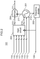
- Figure 2 shows an example of the configuration of the microwave pulse generator 101 in Example 1.
- the microwave pulse generator 101 has a frequency generator 201, frequency divider 202, logic circuit 203, and RFDAC 204.
- the frequency generator 201 receives the reference clock 112, frequency setting signal 113, and frequency modulation signal 214, and outputs sine wave 211 and sine wave 212 with the center frequency and phase set by the frequency setting signal 113 and the frequency generator 201.
- the frequency divider 202 outputs a system clock 124 divided by the frequency of the sine wave 212.
- the logic circuit 203 operates in synchronization with the system clock 124 and outputs pulse data 213 to the RFDAC 204 based on the pulse waveform setting signal 115 and pulse width setting signal 116 at the rise timing of the pulse trigger signal 114.
- the logic circuit 203 also outputs modulation signal 214 to frequency generator201 during the period based on signal 116, based on the phase setting signal 117 and frequency offset setting signal 118 at the timing of the pulse trigger signal 114
- RFDAC Radio Frequency Digital to Analog Converter
- the frequency generator 201 operates at the same frequency as the angular frequencies other than the selected quantum bit except when outputting pulses, and the phase difference is also constant, so that it operates in pseudo-synchronization with the quantum bit.
- the pulse width is a value determined by the system clock 124, the phase shift caused by the frequency modulation signal 214 can be calculated and cancelled. Therefore, it is possible to restore the original phase difference even when the center frequency of frequency generator 201 is the same as the selected quantum bit and is changed from the angular frequency of the other quantum bit.
- Figure 3 shows an example of the configuration of frequency generator 201 in Figure 2 .
- the frequency generator 201 is a PLL (Phase Locked Loop) configuration and assumes a 2-point modulation scheme because of the need to switch phases at high speed.
- PLL Phase Locked Loop
- an analog Type 2 PLL is used as an example, but a digital PLL or sub-sampling PLL can also be implemented.
- the frequency generator 201 shown in Figure 3 consists of a VCO (Voltage Controlled Oscillator) 301, buffer 302, buffer 303, MMD (Multi Modulus Divider) 304, SDM (Sigma Delta Modulator) 305, PFD (Phase Frequency Detector) 306, CP (Charge Pump) 307, LPF (Low Pass Filter) 308, adder 309, DAC (Digital to Analog Converter) 310, SDM (Sigma Delta Modulator) 311, gain adjustment 312, gain adjustment 313, and adder 314.
- VCO Voltage Controlled Oscillator
- MMD Multi Modulus Divider
- SDM Sigma Delta Modulator
- PFD Phase Frequency Detector
- CP Charge Pump
- LPF Low Pass Filter
- adder 309 Digital to Analog Converter
- SDM Sigma Delta Modulator
- the frequency modulation signal 214 is divided into two paths. One path performs gain adjustment to cancel the gain of VCO 301 by the gain adjustment 312, and concerts the signal modulated by SDM 311 to a voltage by DAC 310, and then modulates the frequency of VCO 301 through adder 309 . In the other path, after adjusting the gain with gain adjustment 313, the signal is added to the frequency setting signal 113 with adder 314, and the signal modulated with SDM 305 is input to MMD 304 to modulate the frequency by changing the frequency divider.
- the PLL operates as follows: VCO 301 oscillates at a frequency corresponding to the input voltage, the output of VCO 301 is divided by MMD 304, and PFD 306 compares the phase between the reference clock 112 and the result divided by MMD 304 to output a signal to increase or decrease the voltage.
- the CP 307 can either draw in or draw out current based on the signal from the PFD 306.
- LPF 308 suppresses the high-frequency component of the CP 307 signal to make it a stable voltage and supplies it to VCO 301.
- VCO 301 Since the reference clock 112 and the clock divided by MMD 304 are in phase, the output frequency of VCO 301 is locked to a fractional multiple of the frequency of reference clock 112. Sine wave output from VCO 301 is output as sine wave211 via buffer 302 and output as sine wave 212 through buffer 303.
- frequency modulation signal 214 will be an all-path characteristic for the VCO 301 output, and a sine wave with the set phase and offset frequency can be obtained.
- Figure 4 shows a first configuration example of the logic circuit 203 in Figure 2 .
- frequency modulation signal 214 changes the output frequency of frequency generator 201, it shifts the phase difference between the frequency generator 201 and a group of quantum bits that are not selected. Therefore, logic circuit 203 has a mechanism to cancel the phase shift caused by the frequency offset.
- the logic circuit 203 has a pulse waveform data generator 401, adder 402, differentiator 403, frequency offset controller 404, adder 405, phase shift compensator 406, and gain adjustment 407, and operates in synchronization with the system clock 124.
- the pulse waveform data generator 401 outputs the pulse waveform data set by the pulse waveform setting signal 115 and the pulse width setting signal 116 by triggering the timing when the pulse trigger signal 114 goes High.
- the phase shift compensator 406 calculates the amount of phase shift based on the pulse width setting signal 116 and frequency offset setting signal 118, and outputs a phase cancel signal after a delay of pulse width + ⁇ from the pulse trigger signal 114.
- adder 405 adds the phase cancellation signal output by phase shift compensator 406 to phase setting signal 117.
- Gain adjustment 407 adjusts the gain of the phase value resulting from the addition by adder 405 and outputs gain adjustment output 412.
- Differentiator 403 calculates the difference between gain adjustment output 412. Adder 402 adds the result of calculation of differentiator 403 and the frequency offset 411 output by the frequency offset controller 404, and output frequency modulation signal 214.
- the frequency offset controller 404 outputs the frequency offset setting signal 118 by triggering the timing of the pulse trigger signal 114, and outputs it for the pulse width period set by the pulse width setting signal, and is set to 0 otherwise.
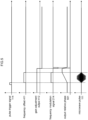
- Figure 5 shows an example of the operation of the logic circuit 203 in Figure 4 .
- the frequency offset controller 404 outputs frequency offset 411 for the pulse width by triggering pulse trigger signal 114.
- the gain adjustment output 412 switches to the value to which the phase shift correction is added with a delay of the pulse width + ⁇ . Therefore, frequency modulation signal 214 outputs the value set by frequency offset 411 at first, and then outputs the differential value of gain adjustment output 412.
- Figure 6 shows an example of the results of simulating the operation of Figure 5 .
- the frequency modulation signal 214 output from adder 402 initially outputs the frequency of frequency offset 411, and the difference is output when gain adjustment output 412 is switched.
- output frequency 601 of frequency generator 201 is the value obtained by adding frequency setting signal 113 to frequency modulation signal 214.
- Output relative phase 501 is fixed at a certain value after the pulse output, but phase correction is added and the phase returns to the phase before the pulse output.
- the phase shift compensator 406 calculates the amount of phase shift based on the pulse width setting signal 116 and frequency offset setting signal 118, outputs the phase cancel signal after a delay of pulse width + ⁇ from the pulse trigger signal 114, and adds it to the phase setting signal 117 at the adder 405. This enables correction of phase shift due to frequency switching of the microwave pulse while reducing the phase error between the quantum bit and the microwave pulse.
- Figure 7 shows a second configuration example of the logic circuit 203 in Figure 2 .
- This method cancels phase shift by outputting two pulses and inverting the frequency offset of each pulse to be positive or negative.
- the logic circuit 203 in Fig. 7 has a pulse waveform data generator 701, adder 702, differentiator 703, frequency offset controller 704, multiplier 705, frequency offset positive/negative switch706, and gain adjustment 707, and operates in synchronization with the system clock 124.
- the pulse waveform data generator 701 outputs the pulse waveform data set by the pulse waveform setting signal 115 and the pulse width setting signal 116 by triggering the timing when the pulse trigger signal 114 goes High.
- the frequency offset controller 704 calculates the output period from the first pulse to the end of the second pulse based on the pulse width setting signal 116, triggers the pulse trigger signal 114, outputs the frequency offset setting signal 118 as frequency offset signal 711 during the output period, and outputs 0 during the other periods.
- the frequency offset positive/negative switch 706 calculates the positive and negative output periods based on the pulse width setting signal 116, and triggers the pulse trigger signal 114 to output the positive signal of positive/negative signal 712 during the positive period and the negative signal of positive/negative signal 712 during the negative output period.
- Multiplier 705 multiplies frequency offset signal 711 and frequency offset positive/negative signal 712 and outputs it to adder 702.
- the adder 702 adjusts the gain of the phase setting signal 117 using gain adjustment 707 and adds the differential value taken by differentiator 703 to the output of adder 702 to produce frequency modulation signal 214.
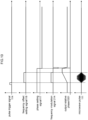
- Figure 8 shows an example of the operation of the logic circuit 203 in Figure 7 .
- the frequency offset controller 704 receives a constant value of frequency offset setting signal 118, triggers pulse trigger signal 114, and outputs frequency offset signal 711 with a width of 2 pulses.
- the frequency offset positive/negative switch 706 outputs a frequency offset positive/negative signal 712, which is a positive signal during the first pulse width period and a negative signal during the next pulse width period.
- the frequency modulation signal 214 has the same width of alternating positive and negative offset frequencies. Therefore, the output relative phase 801 of frequency generator 201 rises and falls during the same period and is equivalent to the phase before the pulse output.
- frequency offset positive/negative switch 706 calculates positive and negative output periods based on pulse width setting signal 116, triggers pulse trigger signal 114, and outputs frequency offset positive/negative signal 712 of a positive signal in the positive output period and a negative signal in the negative output period. This allows phase shift due to frequency switching of the microwave pulse to be corrected while reducing the phase error between the quantum bit and the microwave pulse.
- Figure 9 shows a third configuration example of the logic circuit 203 in Figure 2 .
- the logic circuit 203 does not have a circuit that controls the signal, but instead switches the setting signal pulse by pulse with a microprocessor or control logic circuit outside the logic circuit 203.
- the logic circuit 203 in Figure 9 has a pulse waveform data generator 901, adder 902, differentiator 903, and gain adjustment 904.
- Figure 10 shows the waveforms when the configuration in Figure 9 is made to operate in the same manner as the configuration in Figure 4 .
- Figure 10 shows an example of the operation of the logic circuit 203 in Figure 9 .
- a microprocessor or control logic circuit external to logic circuit 203 triggers pulse trigger signal 114 to set frequency offset setting signal 118 to the desired frequency offset value for the pulse width period.
- the phase setting signal 117 is changed after the pulse width period so that the phase returns to the same value as before the pulse output.
- the frequency modulation signal 214 is determined by the frequency offset setting signal 118 and the phase setting signal 117. Therefore, the output relative phase 1001 to the frequency determined by the frequency setting signal 113 of frequency generator 201 is changed by the frequency offset setting signal 118, but the phase setting signal 117 cancels it and returns to the same phase as before the pulse output.
- a microprocessor, control logic circuit, or the like external to logic circuit 203 triggers pulse trigger signal 114 to set frequency offset setting signal 118 to the desired frequency offset value for the pulse width period.
- the phase setting signal 117 is changed after the pulse width period so that the phase returns to the same value as before the pulse output. This allows phase shift due to frequency switching of the microwave pulse to be corrected while reducing the phase error between the quantum bit and the microwave pulse.
- Figure 11 shows the waveforms when the configuration in Figure 9 is made to operate in the same manner as the configuration in Figure 8 .
- Figure 11 shows another example of the operation of the logic circuit 203 in Figure 9 .
- a microprocessor or control logic circuit external to logic circuit 203 triggers pulse trigger signal 114 and outputs frequency offset setting signal 118 with positive and negative pulses for the first and second pulses, and cancels phase shift due to frequency offset. For example, if the frequency offset is positive for the first pulse, the absolute value is the same for the second pulse but negative.
- a microprocessor, control logic circuit, etc. external to the logic circuit 203 triggers pulse trigger signal 114 and outputs frequency offset setting signal 118 with the first and second pulse reserved positive and negative. This allows phase shift due to frequency switching of the microwave pulse to be corrected while reducing the phase error between the quantum bit and the microwave pulse.
- Figure 12 shows an example of the configuration of microwave pulse generator 101 in Example 2.
- the microwave pulse generator 101 in Example 2 does not require the use of a high-speed DAC and is easier to design than the microwave pulse generator 101 of Example 1 in Figure 2 .
- the microwave pulse generator 101 in Figure 12 has a frequency generator 201, frequency divider 202, logic circuit 203, DAC 1201, and mixer 1202.
- DAC 1201 operates in synchronization with system clock 124, receives pulse data 213, converts it into an analog signal, and outputs it.
- the mixer 1202 modulates the analog signal output by the DAC 1201 with sine wave 211 and outputs a signal having the frequency of sine wave 211 as the center frequency as microwave pulse 111.
- Example 2 the design is easier because the microwave pulse generator 101 has a DAC 1201 and a mixer 1202 instead of a high-speed DAC. In addition, since a high-speed DAC is not used, power consumption can be reduced.
- Figure 13 shows an example of the configuration of microwave pulse generator 101 in Example 3.
- Example 3 shows an example of using an IQ modulation scheme instead of a polar modulation scheme as in Examples 1 and 2.
- the frequency generator 1301 does not need to perform phase cancellation because the frequency is always the same as the quantum bit that is not selected.
- power consumption is larger than in Examples 1 and 2.
- phase errors are caused by IQ imbalance, so IQ imbalance calibration is required.
- the microwave pulse generator 101 has a frequency generator 1301, frequency divider 1302, logic circuit 1303, I-side DAC 1304, Q-side DAC 1305 IQ modulator 1306, IQ demodulator 1307, I-side ADC 1308, Q-side ADC 1309, and calibration circuit 1310.
- the frequency generator 1301 is assumed to be a PLL (Phase Locked Loop) circuit. Frequency generator 1301 generates the frequency output set by frequency setting signal 113 in accordance with reference clock 112. The frequency generator 1301 provides LO output sine wave 1315 and LO output cosine wave 1316 with a 90° phase difference to IQ modulator 1306 and IQ demodulator 1307.
- PLL Phase Locked Loop
- the frequency divider 1302 receives the output of the frequency generator 1301, divides the frequency, and generates the system clock 124.
- the logic circuit 1303 operates in synchronization with the system clock 124 and generates cosine and sine waves with the phase and frequency set by the phase setting signal 117 and frequency offset setting signal 118 at the rise timing of the pulse trigger signal 114.
- the cosine and sine wave is multiplied by the pulses set by the pulse waveform setting signal 115 and pulse width setting signal 116, respectively.
- the I modulation data 1311 is output to the I-side DAC 1304, and Q modulation data 1312 is output to the Q-side DAC 1305, respectively.
- Both I-side DAC 1304 and Q-side DAC 1305 receive I modulation data 1311 and Q modulation data 1312 from logic circuit 1303 at the timing of system clock 124, convert them to analog values, and output them to IQ modulator 1306.
- IQ modulator 1306 multiplies I modulation signal 1313 output by I-side DAC 1304 and Q modulation signal 1314 output by Q-side DAC 1305 with LO output sine wave 1315 and LO output cosine wave 1316 of frequency generator 1301, which have 90° phase difference from each other, respectively, and outputs a phase-modulated microwave pulse 111.
- IQ demodulator 1307 multiplies microwave pulse 111 with LO output sine wave 1315 and LO output cosine wave 1316 to demodulate I demodulation signal 1317 and Q demodulation signal 1318.
- I-side ADC 1308 demodulates I demodulation signal 1317 to I demodulation data 1319 and Q-side ADC 1309 demodulates Q demodulation signal 1318 to Q demodulation data 1320 from analog to digital data.
- the calibration circuit 1310 controls the logic circuit 1303 to set the phase setting signal for calibration 1322, obtains I demodulation data 1319 and Q demodulation data 1320 and calculates IQ gain error and phase error and outputs IQ correction data 1323 to logic circuit 1303.
- Figure 14 shows an example of the configuration of the logic circuit 1303 in Figure 13 .
- the microwave pulse generator 101 has a pulse waveform data generator 1401, selector 1409, multiplier 1402, multiplier 1403, IQ imbalance compensator 1404, cosine/sine table 1405, selector 1408, adder 1406, and frequency/phase converter 1407.
- the frequency/phase converter 1407 triggers the pulse trigger signal 114 and converts the frequency offset setting signal 118 to the period specified by the pulse width setting signal 116.
- Adder 1406 adds the phase 1411 and the phase setting signal 117.
- Selector 1408 passes the phase setting signal for calibration 1322 as phase data 1412 during the calibration period by calibration control signal 1321, and passes the addition result of adder 1406 as phase data 1412 outside the calibration period.
- the cosine/sine table 1405 converts phase data 1412 into cosine wave data 1413 and sine wave data 1414.
- IQ imbalance compensator 1404 corrects and outputs cosine wave data 1413 and sine wave data 1414 using IQ correction data 1323.
- the pulse waveform data generator 1401 generates pulse waveform data based on the pulse waveform setting signal 115 and pulse width setting signal 116, triggered by the pulse trigger signal 114.
- Selector 1409 outputs a fixed value during the calibration period defined by calibration control signal 1321, and outputs pulse waveform data 1415 generated by pulse waveform data generator 1401 during the rest of the calibration period.
- the pulse waveform data 1415 is multiplied by the cosine wave data 1413 corrected by multiplier 1402 and the sine wave data 1414 corrected by multiplier 1403, and output as I modulation data 1311 and Q modulation data 1312, respectively.
- the phase to be set is ⁇
- the phase shift between LO output sine wave 1315, LO output cosine wave 1316 and I modulation signal 1313, Q modulation signal1314 is ⁇
- the angular frequency of the LO output signal is ⁇
- the amplitude of the IQ is A
- the gain error between the IQs is ⁇ A
- the error from the 90° phase of the LO output is ⁇
- the I modulation signal 1313 is represented by Formula 1
- the Q modulation signal 1314 by Formula 2.
- LO output cosine wave 1316 is represented by Formula 3, LO output sine wave 1315 by Formula 4, and microwave pulse 111 by Formula 5. If the phase difference of LO output cosine wave 1316 and LO output sine wave 1315 between IQ modulator 1306 and IQ demodulator 1307 is ⁇ D, I demodulation signal 1317 is represented by Formula 6 and Q demodulation signal 1318 by Formula7.
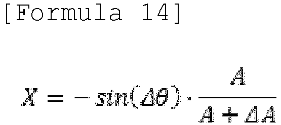
- the IQ imbalance compensator 1404 outputs the cosine wave data 1413 as it is, and the sine wave data side can be corrected by adding the cosine wave data 1413 multiplied by Formula 14 and the sine wave data 1414 multiplied by Formula 15.
- X ⁇ sin ⁇ ⁇ A A + ⁇ A
- Y cos ⁇ ⁇ A A + ⁇ A
- Figure 15 shows an example of the normal operation of the logic circuit 1303 in Figure 14 .
- phase 1411 is added to phase setting signal 117 by adder 1406, and phase data 1412 is output by selector 1408.
- Cosine wave data 1413 and sine wave data 1414 are generated from phase data 1412 by cosine/sine table 1405 and multiplied with pulse waveform data 1415 by multipliers 1402 and 1403, I modulation data 1311 and Q modulation data 1312 are output respectively.
- Figure 16 shows an example of the operation of the logic circuit 1303 in Figure 14 during calibration.
- calibration is performed while the calibration control signal 1321 is High, with the phase setting signal for calibration 1322 changed to 0° , 90° , 180° , 270° , and IQ correction data 1323 is finally calculated and output.
- calibration circuit 1310 acquires I demodulation data 1319 and Q demodulation data 1320, calculates IQ gain error and phase error, and outputs IQ correction data to logic circuit 1303.
- IQ imbalance compensator 1404 uses IQ correction data 1323 to correct cosine wave data 1413 and sine wave data 1414 and output them. This reduces the phase error between the quantum bit and the microwave pulse.
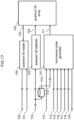
- Figure 17 shows an example of the quantum computer configuration in Example 4.
- Example 4 when there is a small frequency shift between the quantum bits in the quantum bit array, data to correct the phase shift caused by the frequency shift is added to microwave pulse 111 and output.
- the quantum computer in Figure 17 has phase correction data 1701 in addition to the configuration in Figure 1 .
- Quantum bit address signal 119 is put into phase correction data 1701, and then phase correction is added, frequency setting signal 113 is input to the microwave pulse generator 101.
- the microwave pulse generator 101 has the same configuration as in Figure 2 .
- Frequency generator 201 outputs a sine wave based on the phase-corrected frequency setting signal 113.
- RFDAC 204 modulates pulse data 213 by the sine wave 211 and outputs a signal with the frequency of the sine wave 211 as the center frequency as microwave pulse111.
- the quantum bit address signal 119 is put into the phase correction data 1701, phase correction is added, and the frequency setting signal 113 is input to the microwave pulse generator 101. This allows correction of minute frequency deviations between the quantum bits in the quantum bit array.
- the present invention is not limited to the above examples, but includes various variations.
- the above examples are described in detail for the purpose of explaining the invention in an easy-to-understand manner, and are not necessarily limited to those having all the described configurations. It is also possible to replace a part of the configuration of one example with that of another example, and it is also possible to add the configuration of another example to that of one example. It is also possible to add, delete, or replace some of the configurations of each example with other configurations.
Landscapes
- Engineering & Computer Science (AREA)
- Physics & Mathematics (AREA)
- General Physics & Mathematics (AREA)
- Theoretical Computer Science (AREA)
- Mathematical Optimization (AREA)
- Pure & Applied Mathematics (AREA)
- Data Mining & Analysis (AREA)
- Evolutionary Computation (AREA)
- Computational Mathematics (AREA)
- Mathematical Analysis (AREA)
- Artificial Intelligence (AREA)
- Condensed Matter Physics & Semiconductors (AREA)
- Computing Systems (AREA)
- General Engineering & Computer Science (AREA)
- Mathematical Physics (AREA)
- Software Systems (AREA)
- Nonlinear Science (AREA)
- Digital Transmission Methods That Use Modulated Carrier Waves (AREA)
- Radar Systems Or Details Thereof (AREA)
- Stabilization Of Oscillater, Synchronisation, Frequency Synthesizers (AREA)
Abstract
Description
- The invention relates to a microwave pulse generator that generates phase adjustable microwaves for operating a quantum bit and quantum computer.
- As the limits of semiconductor miniaturization are becoming visible, we are reaching the limit of relying on semiconductor miniaturization to improve von Neumann-type computers. For this reason, attention is focusing on computers that operate on a different principle than the von Neumann type and that can solve specific problems at high speeds. As one such example, the quantum computer is being developed.
- A quantum computer uses information such as energy states of devices that can superimpose states called quantum bits and performs calculations by manipulating the state probabilities of quantum bits. Quantum bits include those that use superconductivity and those that use electron spin. For electron spin, two energy states are used as information.
- Electrons are in precessional motion with a certain magnetic moment, and when a strong magnetic field is applied to the electrons from outside, two energy states, upward spin and downward spin, are generated. In this case, the angular frequency of the spin of the electron changes depending on the strength of the magnetic field. During the coherence time, the upward and downward spins are in a superposition state. By applying a radio frequency (RF) field of the same frequency as the angular frequency, the probabilities of the two energy states can be manipulated. When an RF field applied, the two spin state probabilities undergo Rabi oscillations that vary sinusoidally with the energy given. Therefore, it is necessary to control the energy and phase of the RF magnetic field in order to manipulate the two spin state probabilities to the required state probabilities.
- The microwave pulse generator, which generates the RF magnetic field by microwave pulse irradiation, uses an IQ modulator to allow phase control as well (see
US2018/0013426 ,US2020/0034736 ) . - In the microwave pulse generator of
US2018/0013426 andUS2020/0034736 , the IQ modulator can control the phase by changing the amplitude of RF signals with 90° phase difference. However, the 90° phase difference can be slightly shifted or the signal amplitudes on the I and Q sides can be misaligned, resulting in phase errors. Quantum manipulations are performed several times during the coherence time of a quantum bit. The phase difference between the microwave pulse and the precession of the quantum bit must be kept constant. Therefore, the phase error leads to a degradation of the accuracy of the quantum manipulation. - Because microwave pulses irradiated spatially spread out, multiple quantum bits are operated simultaneously when quantum bits are integrated. Therefore, control is performed so that the angular frequency is changed between the quantum bit to be manipulated and other quantum bits. In this case, the output phase of the microwave pulse generator is also changed by the frequency switch.
- In a quantum computer using electron spins, the microwave pulse that performs quantum manipulation needs to minimize the phase error during quantum manipulation while maintaining the phase difference with the quantum bit during the coherence time. Furthermore, the frequency switching during quantum manipulation causes phase shift, which is an issue.
- Therefore, the purpose of this invention is to provide a technique that can correct the phase shift due to frequency switching of the microwave pulse while reducing the phase error between the quantum bit and the microwave pulse.
- To solve the above problem, one of the typical quantum computers of the present invention is a quantum computer comprising a quantum bit array with multiple quantum bits, a quantum bit selector that selects a quantum bit to be quantum manipulated from the quantum bit array and shifts the angular frequency, and a microwave pulse generator that has the same frequency as the selected quantum bit and outputs a microwave pulse with a set pulse width and pulse amplitude, wherein the microwave pulse generator comprises, a logic circuit that outputs pulse data of the set pulse width and pulse amplitude, a frequency generator that outputs a sine wave having the same frequency as the selected quantum bit, a converter that converts the pulse data into an analog signal, modulates it with the sine wave, and outputs a signal having the frequency of the sine wave as the center frequency as a microwave pulse, and a frequency divider that outputs a system clock divided by the frequency of the sine wave, wherein the frequency generator operates at the same frequency as the quantum bit other than the selected quantum bit except when the microwave pulse is output, and the logic circuit operates in synchronization with the system clock.
- According to the present invention, phase shift due to frequency switching of the microwave pulse can be corrected while reducing the phase error between the quantum bit and the microwave pulse.
- Issues, configurations and effects other than those described above will be clarified in the following description of embodiments.
-
-
Fig. 1 is a block diagram showing an example of the configuration of a quantum computer in Example 1. -
Fig. 2 shows an example of the configuration of themicrowave pulse generator 101 in Example 1. -
Fig. 3 shows an example of the configuration offrequency generator 201 inFig. 2 . -
Fig. 4 shows a first example of the configuration of thelogic circuit 203 inFig. 2 . -
Fig. 5 shows an example of the operation of thelogic circuit 203 inFig. 4 . -
Fig. 6 shows an example of the results of simulating the operation shown inFig. 5 . -
Fig. 7 shows a second configuration example of thelogic circuit 203 inFig. 2 . -
Fig. 8 shows an example of the operation of thelogic circuit 203 inFig. 7 . -
Fig. 9 shows a third configuration example of thelogic circuit 203 inFig. 2 . -
Fig. 10 shows an example of the operation of thelogic circuit 203 inFig. 9 . -
Fig. 11 shows another example of the operation of thelogic circuit 203 inFig. 9 . -
Fig. 12 shows an example of the configuration of amicrowave pulse generator 101 in Example 2. -
Fig. 13 shows an example of the configuration of amicrowave pulse generator 101 in Example 3. -
Fig. 14 shows an example of the configuration of thelogic circuit 1303 inFig. 13 . -
Fig. 15 shows an example of the normal operation of thelogic circuit 1303 inFig. 14 . -
Fig. 16 shows an example of the operation during calibration of thelogic circuit 1303 inFig. 14 . -
Fig. 17 shows an example of the configuration of a quantum computer in Example 4. - Examples are described below using the drawings.
-
Figure 1 is a block diagram showing an example of the configuration of a quantum computer in Example 1. - The quantum computer comprises a
quantum bit array 102 that holds information, amicrowave pulse generator 101 that manipulates thequantum bit array 102, aquantum bit selector 103 that selects a quantum bit to be manipulated from thequantum bit array 102, and aquantum bit reader 104 that reads out the result manipulated by themicrowave pulse generator 101 from the selected quantum bit in thequantum bit array 102. - The
quantum bit array 102 has multiple quantum bits arranged in array form. The quantum bits selected by the quantumbit selection signal 120 are operated by irradiatingmicrowave pulses 111. And the operatedquantum bit state 123 is read out by quantum bit reader104. - The
microwave pulse generator 101 receivesreference clock 112,frequency setting signal 113,pulse trigger signal 114, pulsewaveform setting signal 115, pulsewidth setting signal 116,phase setting signal 117, and frequencyoffset setting signal 118. - The
microwave pulse generator 101 outputs amicrowave pulse 111 with a center frequency equal to the sum of thefrequency setting signal 113 and the frequencyoffset setting signal 118, a phase offset set by thephase setting signal 117, and a pulse width set by the pulsewidth setting signal 116, and a pulse shape that includes an amplitude set by the pulsewaveform setting signal 115, at the input timing of thepulse trigger signal 114. , - The
microwave pulse 111 is made to resonate by having a frequency that matches the selected quantum bit, and the state probability of the selected quantum bit is manipulated by the pulse width and pulse amplitude. - The
microwave pulse generator 101 also outputssystem clock 124, which provides a clock for synchronization to circuits that perform logic operations. - The
quantum bit selector 103 receives the quantumbit address signal 119 and outputs the quantumbit selection signal 120 to select the quantum bit to be quantum manipulated from thequantum bit array 102. In doing so, the angular frequency of the quantum bit to be selected is shifted or otherwise made selectable. - The
quantum bit reader 104 receives thecontrol signal 121, reads thequantum bit state 123 from thequantum bit array 102, and outputs the quantum bit readout results 122. -
Figure 2 shows an example of the configuration of themicrowave pulse generator 101 in Example 1. - The
microwave pulse generator 101 has afrequency generator 201,frequency divider 202,logic circuit 203, andRFDAC 204. - The
frequency generator 201 receives thereference clock 112,frequency setting signal 113, andfrequency modulation signal 214, andoutputs sine wave 211 andsine wave 212 with the center frequency and phase set by thefrequency setting signal 113 and thefrequency generator 201. - The
frequency divider 202 outputs asystem clock 124 divided by the frequency of thesine wave 212. - The
logic circuit 203 operates in synchronization with thesystem clock 124 and outputs pulsedata 213 to theRFDAC 204 based on the pulsewaveform setting signal 115 and pulsewidth setting signal 116 at the rise timing of thepulse trigger signal 114. Thelogic circuit 203 also outputsmodulation signal 214 to frequency generator201 during the period based onsignal 116, based on thephase setting signal 117 and frequency offset settingsignal 118 at the timing of thepulse trigger signal 114 - RFDAC (Radio Frequency Digital to Analog Converter) 204 receives
pulse data 213, convertspulse data 213 to an analog signal, modulates it withsine wave 211, and outputs a signal with the frequency ofsine wave 211 as the center frequency asmicrowave pulse 111. - The
frequency generator 201 operates at the same frequency as the angular frequencies other than the selected quantum bit except when outputting pulses, and the phase difference is also constant, so that it operates in pseudo-synchronization with the quantum bit. - Since the pulse width is a value determined by the
system clock 124, the phase shift caused by thefrequency modulation signal 214 can be calculated and cancelled. Therefore, it is possible to restore the original phase difference even when the center frequency offrequency generator 201 is the same as the selected quantum bit and is changed from the angular frequency of the other quantum bit. -
Figure 3 shows an example of the configuration offrequency generator 201 inFigure 2 . - The
frequency generator 201 is a PLL (Phase Locked Loop) configuration and assumes a 2-point modulation scheme because of the need to switch phases at high speed. In this example, an analog Type 2 PLL is used as an example, but a digital PLL or sub-sampling PLL can also be implemented. - The
frequency generator 201 shown inFigure 3 consists of a VCO (Voltage Controlled Oscillator) 301,buffer 302,buffer 303, MMD (Multi Modulus Divider) 304, SDM (Sigma Delta Modulator) 305, PFD (Phase Frequency Detector) 306, CP (Charge Pump) 307, LPF (Low Pass Filter) 308,adder 309, DAC (Digital to Analog Converter) 310, SDM (Sigma Delta Modulator) 311,gain adjustment 312,gain adjustment 313, andadder 314. - The
frequency modulation signal 214 is divided into two paths. One path performs gain adjustment to cancel the gain ofVCO 301 by thegain adjustment 312, and concerts the signal modulated bySDM 311 to a voltage byDAC 310, and then modulates the frequency ofVCO 301 throughadder 309 . In the other path, after adjusting the gain withgain adjustment 313, the signal is added to thefrequency setting signal 113 withadder 314, and the signal modulated withSDM 305 is input toMMD 304 to modulate the frequency by changing the frequency divider. - The PLL operates as follows:
VCO 301 oscillates at a frequency corresponding to the input voltage, the output ofVCO 301 is divided byMMD 304, andPFD 306 compares the phase between thereference clock 112 and the result divided byMMD 304 to output a signal to increase or decrease the voltage. TheCP 307 can either draw in or draw out current based on the signal from thePFD 306.LPF 308 suppresses the high-frequency component of theCP 307 signal to make it a stable voltage and supplies it toVCO 301. - Since the
reference clock 112 and the clock divided byMMD 304 are in phase, the output frequency ofVCO 301 is locked to a fractional multiple of the frequency ofreference clock 112. Sine wave output fromVCO 301 is output as sine wave211 viabuffer 302 and output assine wave 212 throughbuffer 303. - Next, for 2-point modulation, since the path through
DAC 310 passes only high-frequency components and the path throughSDM 305 passes only low-frequency components, if the timing and gain of these two paths can be matched,frequency modulation signal 214 will be an all-path characteristic for theVCO 301 output, and a sine wave with the set phase and offset frequency can be obtained. -
Figure 4 shows a first configuration example of thelogic circuit 203 inFigure 2 . - Since
frequency modulation signal 214 changes the output frequency offrequency generator 201, it shifts the phase difference between thefrequency generator 201 and a group of quantum bits that are not selected. Therefore,logic circuit 203 has a mechanism to cancel the phase shift caused by the frequency offset. - The
logic circuit 203 has a pulsewaveform data generator 401,adder 402,differentiator 403, frequency offsetcontroller 404,adder 405,phase shift compensator 406, andgain adjustment 407, and operates in synchronization with thesystem clock 124. - The pulse
waveform data generator 401 outputs the pulse waveform data set by the pulsewaveform setting signal 115 and the pulsewidth setting signal 116 by triggering the timing when thepulse trigger signal 114 goes High. - The
phase shift compensator 406 calculates the amount of phase shift based on the pulsewidth setting signal 116 and frequency offset settingsignal 118, and outputs a phase cancel signal after a delay of pulse width +α from thepulse trigger signal 114.
adder 405 adds the phase cancellation signal output byphase shift compensator 406 to phase settingsignal 117.Gain adjustment 407 adjusts the gain of the phase value resulting from the addition byadder 405 and outputs gainadjustment output 412. -
Differentiator 403 calculates the difference betweengain adjustment output 412.Adder 402 adds the result of calculation ofdifferentiator 403 and the frequency offset 411 output by the frequency offsetcontroller 404, and outputfrequency modulation signal 214. - The frequency offset
controller 404 outputs the frequency offset settingsignal 118 by triggering the timing of thepulse trigger signal 114, and outputs it for the pulse width period set by the pulse width setting signal, and is set to 0 otherwise. -
Figure 5 shows an example of the operation of thelogic circuit 203 inFigure 4 . - The frequency offset
controller 404 outputs frequency offset 411 for the pulse width by triggeringpulse trigger signal 114. Thegain adjustment output 412 switches to the value to which the phase shift correction is added with a delay of the pulse width +α. Therefore,frequency modulation signal 214 outputs the value set by frequency offset 411 at first, and then outputs the differential value ofgain adjustment output 412. - At this time, the output phase of
frequency generator 201 is changed and then cancelled to the original phase, as in outputrelative phase 501 to the frequency set byfrequency setting signal 113. -
Figure 6 shows an example of the results of simulating the operation ofFigure 5 . - The
frequency modulation signal 214 output fromadder 402 initially outputs the frequency of frequency offset 411, and the difference is output whengain adjustment output 412 is switched. At this time,output frequency 601 offrequency generator 201 is the value obtained by addingfrequency setting signal 113 tofrequency modulation signal 214. Outputrelative phase 501 is fixed at a certain value after the pulse output, but phase correction is added and the phase returns to the phase before the pulse output. - According to the first configuration example of
logic circuit 203 described inFigures 4 to 6 , thephase shift compensator 406 calculates the amount of phase shift based on the pulsewidth setting signal 116 and frequency offset settingsignal 118, outputs the phase cancel signal after a delay of pulse width +α from thepulse trigger signal 114, and adds it to thephase setting signal 117 at theadder 405. This enables correction of phase shift due to frequency switching of the microwave pulse while reducing the phase error between the quantum bit and the microwave pulse. -
Figure 7 shows a second configuration example of thelogic circuit 203 inFigure 2 . - This method cancels phase shift by outputting two pulses and inverting the frequency offset of each pulse to be positive or negative.
- The
logic circuit 203 inFig. 7 has a pulsewaveform data generator 701,adder 702,differentiator 703, frequency offsetcontroller 704,multiplier 705, frequency offset positive/negative switch706, andgain adjustment 707, and operates in synchronization with thesystem clock 124. - The pulse
waveform data generator 701 outputs the pulse waveform data set by the pulsewaveform setting signal 115 and the pulsewidth setting signal 116 by triggering the timing when thepulse trigger signal 114 goes High. - The frequency offset
controller 704 calculates the output period from the first pulse to the end of the second pulse based on the pulsewidth setting signal 116, triggers thepulse trigger signal 114, outputs the frequency offset settingsignal 118 as frequency offsetsignal 711 during the output period, andoutputs 0 during the other periods. - The frequency offset positive/
negative switch 706 calculates the positive and negative output periods based on the pulsewidth setting signal 116, and triggers thepulse trigger signal 114 to output the positive signal of positive/negative signal 712 during the positive period and the negative signal of positive/negative signal 712 during the negative output period. -
Multiplier 705 multiplies frequency offsetsignal 711 and frequency offset positive/negative signal 712 and outputs it to adder 702. - The
adder 702 adjusts the gain of thephase setting signal 117 usinggain adjustment 707 and adds the differential value taken bydifferentiator 703 to the output ofadder 702 to producefrequency modulation signal 214. -
Figure 8 shows an example of the operation of thelogic circuit 203 inFigure 7 . - The frequency offset
controller 704 receives a constant value of frequency offset settingsignal 118, triggerspulse trigger signal 114, and outputs frequency offsetsignal 711 with a width of 2 pulses. - The frequency offset positive/
negative switch 706 outputs a frequency offset positive/negative signal 712, which is a positive signal during the first pulse width period and a negative signal during the next pulse width period. - The
frequency modulation signal 214 has the same width of alternating positive and negative offset frequencies. Therefore, the output relative phase 801 offrequency generator 201 rises and falls during the same period and is equivalent to the phase before the pulse output. - According to the second configuration example of
logic circuit 203 described inFigures 7 and8 , frequency offset positive/negative switch 706 calculates positive and negative output periods based on pulsewidth setting signal 116, triggerspulse trigger signal 114, and outputs frequency offset positive/negative signal 712 of a positive signal in the positive output period and a negative signal in the negative output period. This allows phase shift due to frequency switching of the microwave pulse to be corrected while reducing the phase error between the quantum bit and the microwave pulse. -
Figure 9 shows a third configuration example of thelogic circuit 203 inFigure 2 . - In the third example, the
logic circuit 203 does not have a circuit that controls the signal, but instead switches the setting signal pulse by pulse with a microprocessor or control logic circuit outside thelogic circuit 203. - The
logic circuit 203 inFigure 9 has a pulsewaveform data generator 901,adder 902,differentiator 903, andgain adjustment 904. -
Figure 10 shows the waveforms when the configuration inFigure 9 is made to operate in the same manner as the configuration inFigure 4 . -
Figure 10 shows an example of the operation of thelogic circuit 203 inFigure 9 . - A microprocessor or control logic circuit external to
logic circuit 203 triggerspulse trigger signal 114 to set frequency offset settingsignal 118 to the desired frequency offset value for the pulse width period. Thephase setting signal 117 is changed after the pulse width period so that the phase returns to the same value as before the pulse output. - The
frequency modulation signal 214 is determined by the frequency offset settingsignal 118 and thephase setting signal 117. Therefore, the output relative phase 1001 to the frequency determined by thefrequency setting signal 113 offrequency generator 201 is changed by the frequency offset settingsignal 118, but thephase setting signal 117 cancels it and returns to the same phase as before the pulse output. - According to the example in
Fig. 10 , a microprocessor, control logic circuit, or the like external tologic circuit 203 triggerspulse trigger signal 114 to set frequency offset settingsignal 118 to the desired frequency offset value for the pulse width period. Thephase setting signal 117 is changed after the pulse width period so that the phase returns to the same value as before the pulse output. This allows phase shift due to frequency switching of the microwave pulse to be corrected while reducing the phase error between the quantum bit and the microwave pulse. -
Figure 11 shows the waveforms when the configuration inFigure 9 is made to operate in the same manner as the configuration inFigure 8 . -
Figure 11 shows another example of the operation of thelogic circuit 203 inFigure 9 . - A microprocessor or control logic circuit external to
logic circuit 203 triggerspulse trigger signal 114 and outputs frequency offset settingsignal 118 with positive and negative pulses for the first and second pulses, and cancels phase shift due to frequency offset. For example, if the frequency offset is positive for the first pulse, the absolute value is the same for the second pulse but negative. - This changes the output relative phase 1101 after the first pulse output, but returns to the phase before the first pulse output after the second pulse output.
- According to the example in
Figure 11 , a microprocessor, control logic circuit, etc. external to thelogic circuit 203 triggerspulse trigger signal 114 and outputs frequency offset settingsignal 118 with the first and second pulse reserved positive and negative. This allows phase shift due to frequency switching of the microwave pulse to be corrected while reducing the phase error between the quantum bit and the microwave pulse. -
Figure 12 shows an example of the configuration ofmicrowave pulse generator 101 in Example 2. - The
microwave pulse generator 101 in Example 2 does not require the use of a high-speed DAC and is easier to design than themicrowave pulse generator 101 of Example 1 inFigure 2 . - The
microwave pulse generator 101 inFigure 12 has afrequency generator 201,frequency divider 202,logic circuit 203,DAC 1201, andmixer 1202. -
DAC 1201 operates in synchronization withsystem clock 124, receivespulse data 213, converts it into an analog signal, and outputs it. - The
mixer 1202 modulates the analog signal output by theDAC 1201 withsine wave 211 and outputs a signal having the frequency ofsine wave 211 as the center frequency asmicrowave pulse 111. - The configuration other than
DAC 1201 andmixer 1202 is the same as inFigure 2 , and the operation is equivalent to Example 1. - According to Example 2, the design is easier because the
microwave pulse generator 101 has aDAC 1201 and amixer 1202 instead of a high-speed DAC. In addition, since a high-speed DAC is not used, power consumption can be reduced. -
Figure 13 shows an example of the configuration ofmicrowave pulse generator 101 in Example 3. - Example 3 shows an example of using an IQ modulation scheme instead of a polar modulation scheme as in Examples 1 and 2.
- In the third example, the
frequency generator 1301 does not need to perform phase cancellation because the frequency is always the same as the quantum bit that is not selected. However, since the number of blocks is large, power consumption is larger than in Examples 1 and 2. In addition, phase errors are caused by IQ imbalance, so IQ imbalance calibration is required. - Therefore, in Example 3, the
microwave pulse generator 101 has afrequency generator 1301,frequency divider 1302,logic circuit 1303, I-side DAC 1304, Q-side DAC 1305IQ modulator 1306,IQ demodulator 1307, I-side ADC 1308, Q-side ADC 1309, andcalibration circuit 1310. - The
frequency generator 1301 is assumed to be a PLL (Phase Locked Loop) circuit.Frequency generator 1301 generates the frequency output set byfrequency setting signal 113 in accordance withreference clock 112. Thefrequency generator 1301 provides LOoutput sine wave 1315 and LOoutput cosine wave 1316 with a 90° phase difference toIQ modulator 1306 andIQ demodulator 1307. - The
frequency divider 1302 receives the output of thefrequency generator 1301, divides the frequency, and generates thesystem clock 124. - The
logic circuit 1303 operates in synchronization with thesystem clock 124 and generates cosine and sine waves with the phase and frequency set by thephase setting signal 117 and frequency offset settingsignal 118 at the rise timing of thepulse trigger signal 114. The cosine and sine wave is multiplied by the pulses set by the pulsewaveform setting signal 115 and pulsewidth setting signal 116, respectively. And then theI modulation data 1311 is output to the I-side DAC 1304, andQ modulation data 1312 is output to the Q-side DAC 1305, respectively. - Both I-
side DAC 1304 and Q-side DAC 1305 receive Imodulation data 1311 andQ modulation data 1312 fromlogic circuit 1303 at the timing ofsystem clock 124, convert them to analog values, and output them toIQ modulator 1306. -
IQ modulator 1306 multiplies Imodulation signal 1313 output by I-side DAC 1304 andQ modulation signal 1314 output by Q-side DAC 1305 with LOoutput sine wave 1315 and LOoutput cosine wave 1316 offrequency generator 1301, which have 90° phase difference from each other, respectively, and outputs a phase-modulatedmicrowave pulse 111. -
IQ demodulator 1307 multipliesmicrowave pulse 111 with LOoutput sine wave 1315 and LOoutput cosine wave 1316 to demodulate I demodulationsignal 1317 andQ demodulation signal 1318. I-side ADC 1308 demodulates I demodulation signal 1317 to I demodulationdata 1319 and Q-side ADC 1309 demodulatesQ demodulation signal 1318 toQ demodulation data 1320 from analog to digital data. - The
calibration circuit 1310 controls thelogic circuit 1303 to set the phase setting signal forcalibration 1322, obtains I demodulationdata 1319 andQ demodulation data 1320 and calculates IQ gain error and phase error and outputsIQ correction data 1323 tologic circuit 1303. -
Figure 14 shows an example of the configuration of thelogic circuit 1303 inFigure 13 . - The
microwave pulse generator 101 has a pulsewaveform data generator 1401,selector 1409,multiplier 1402,multiplier 1403,IQ imbalance compensator 1404, cosine/sine table 1405,selector 1408,adder 1406, and frequency/phase converter 1407. - The frequency/
phase converter 1407 triggers thepulse trigger signal 114 and converts the frequency offset settingsignal 118 to the period specified by the pulsewidth setting signal 116.Adder 1406 adds thephase 1411 and thephase setting signal 117. -
Selector 1408 passes the phase setting signal forcalibration 1322 asphase data 1412 during the calibration period bycalibration control signal 1321, and passes the addition result ofadder 1406 asphase data 1412 outside the calibration period. - The cosine/sine table 1405 converts
phase data 1412 intocosine wave data 1413 and sine wave data 1414. -
IQ imbalance compensator 1404 corrects and outputs cosinewave data 1413 and sine wave data 1414 usingIQ correction data 1323. - The pulse
waveform data generator 1401 generates pulse waveform data based on the pulsewaveform setting signal 115 and pulsewidth setting signal 116, triggered by thepulse trigger signal 114. -
Selector 1409 outputs a fixed value during the calibration period defined bycalibration control signal 1321, and outputs pulsewaveform data 1415 generated by pulsewaveform data generator 1401 during the rest of the calibration period. - The
pulse waveform data 1415 is multiplied by thecosine wave data 1413 corrected bymultiplier 1402 and the sine wave data 1414 corrected bymultiplier 1403, and output as Imodulation data 1311 andQ modulation data 1312, respectively. - Next, the operation of the
calibration circuit 1310 is described. If the phase to be set is Φ, the phase shift between LOoutput sine wave 1315, LOoutput cosine wave 1316 and Imodulation signal 1313, Q modulation signal1314 is θ, the angular frequency of the LO output signal is ω, and the amplitude of the IQ is A, the gain error between the IQs is ΔA, the error from the 90° phase of the LO output is Δθ, theI modulation signal 1313 is represented byFormula 1 and theQ modulation signal 1314 by Formula 2. - LO
output cosine wave 1316 is represented by Formula 3, LOoutput sine wave 1315 byFormula 4, andmicrowave pulse 111 byFormula 5. If the phase difference of LOoutput cosine wave 1316 and LOoutput sine wave 1315 betweenIQ modulator 1306 andIQ demodulator 1307 is △D, I demodulationsignal 1317 is represented by Formula 6 andQ demodulation signal 1318 by Formula7.


- Consider I demodulation
signal 1317 andQ demodulation signal 1318 at φ=0 and φ=π/2. I demodulation signal 1317 at φ=0 is in Formula 8,Q demodulation signal 1318 at φ=0 is in Formula 9, I demodulationsignal 1317 at φ=π/2 is inFormula 10, andQ demodulation signal 1318 at ϕ=π/2 is in Formula 11.


- From Formula 8 to Formula 11, the gain error △A and phase error △θ are obtained in Formula 12 and
Formula 13.


- The
IQ imbalance compensator 1404 outputs thecosine wave data 1413 as it is, and the sine wave data side can be corrected by adding thecosine wave data 1413 multiplied byFormula 14 and the sine wave data 1414 multiplied byFormula 15.

- Considering the influence of DC offset, I demodulation
data 1319 andQ demodulation data 1320 are obtained and averaged for Φ = 0° , 90° , 180° , and 270° , and the difference between φ = 0° and φ = 180° is treated as the result of Formula 8 and Formula 9, the difference between ϕ=90° and ϕ=90° is treated as the result ofFormula 10 and Formula 11. -
Figure 15 shows an example of the normal operation of thelogic circuit 1303 inFigure 14 . - After the
pulse trigger signal 114 rises, the frequency offset settingsignal 118 changes thephase 1411 output by the frequency/phase converter 1407. Phase1411 is added to phase settingsignal 117 byadder 1406, andphase data 1412 is output byselector 1408. -
Cosine wave data 1413 and sine wave data 1414 are generated fromphase data 1412 by cosine/sine table 1405 and multiplied withpulse waveform data 1415 bymultipliers modulation data 1311 andQ modulation data 1312 are output respectively. -
Figure 16 shows an example of the operation of thelogic circuit 1303 inFigure 14 during calibration. - In the
calibration circuit 1310, calibration is performed while thecalibration control signal 1321 is High, with the phase setting signal forcalibration 1322 changed to 0° , 90° , 180° , 270° , andIQ correction data 1323 is finally calculated and output. - According to Example 3,
calibration circuit 1310 acquires I demodulationdata 1319 andQ demodulation data 1320, calculates IQ gain error and phase error, and outputs IQ correction data tologic circuit 1303.IQ imbalance compensator 1404 usesIQ correction data 1323 to correctcosine wave data 1413 and sine wave data 1414 and output them. This reduces the phase error between the quantum bit and the microwave pulse. -
Figure 17 shows an example of the quantum computer configuration in Example 4. - In Example 4, when there is a small frequency shift between the quantum bits in the quantum bit array, data to correct the phase shift caused by the frequency shift is added to
microwave pulse 111 and output. - The quantum computer in
Figure 17 hasphase correction data 1701 in addition to the configuration inFigure 1 . Quantumbit address signal 119 is put intophase correction data 1701, and then phase correction is added,frequency setting signal 113 is input to themicrowave pulse generator 101. - The
microwave pulse generator 101 has the same configuration as inFigure 2 .Frequency generator 201 outputs a sine wave based on the phase-correctedfrequency setting signal 113.RFDAC 204 modulatespulse data 213 by thesine wave 211 and outputs a signal with the frequency of thesine wave 211 as the center frequency as microwave pulse111. - According to Example 4, the quantum
bit address signal 119 is put into thephase correction data 1701, phase correction is added, and thefrequency setting signal 113 is input to themicrowave pulse generator 101. This allows correction of minute frequency deviations between the quantum bits in the quantum bit array. - The present invention is not limited to the above examples, but includes various variations. For example, the above examples are described in detail for the purpose of explaining the invention in an easy-to-understand manner, and are not necessarily limited to those having all the described configurations. It is also possible to replace a part of the configuration of one example with that of another example, and it is also possible to add the configuration of another example to that of one example. It is also possible to add, delete, or replace some of the configurations of each example with other configurations.
Claims (15)
- A quantum computer, comprising:a quantum bit array with multiple quantum bits,a quantum bit selector that selects a quantum bit to be quantum manipulated from the quantum bit array and shifts the angular frequency, anda microwave pulse generator that has the same frequency as the selected quantum bit and outputs a microwave pulse with a set pulse width and pulse amplitude,wherein the microwave pulse generator comprises,a logic circuit that outputs pulse data of the set pulse width and pulse amplitude,a frequency generator that outputs a sine wave having the same frequency as the selected quantum bit,a converter that converts the pulse data into an analog signal, modulates it with the sine wave, and outputs a signal having the frequency of the sine wave as the center frequency as a microwave pulse, anda frequency divider that outputs a system clock divided by the frequency of the sine wave,wherein the frequency generator operates at the same frequency as the quantum bit other than the selected quantum bit except when the microwave pulse is output, andthe logic circuit operates in synchronization with the system clock.
- The quantum computer according to claim 1,wherein the logic circuit outputs a frequency modulation signal based on the frequency of the selected quantum bit, andthe frequency generator outputs a sine wave based on the frequency modulation signal.
- The quantum computer according to claim 2,
wherein the logic circuit calculates the amount of phase shift based on the set pulse width and the frequency of the selected quantum bit, and outputs a frequency modulation signal based on the amount of phase shift. - The quantum computer according to claim 2,
wherein the logic circuit outputs a frequency modulation signal based on the frequency of the selected quantum bit, and then outputs a frequency modulation signal based on the frequency of the selected quantum bit multiplied by a negative value. - The quantum computer according to claim 2,
wherein the logic circuit acquires the phase setting signal, which is the set phase minus the phase shift amount, from an external source, and outputs a frequency modulation signal based on the acquired phase setting signal. - The quantum computer according to claim 2,
wherein the logic circuit acquires from an external source the frequency offset setting signal of the frequency of the selected quantum bit and the frequency offset signal of the frequency of the selected quantum bit multiplied by a negative value, and outputs a frequency modulation signal based on the acquired frequency offset signal. - The quantum computer according to claim 2, further comprising:phase correction data that corrects the frequency shift of the plurality of quantum bits in the quantum bit array,wherein the frequency generator outputs a sine wave based on the phase correction data of the selected quantum bit.
- The quantum computer according to claim 2,
wherein the converter is an RFDAC. - The quantum computer according to claim 2,
wherein the converters comprisesa DAC that converts the pulse data into an analog signal, anda mixer that modulates the analog signal with the sine wave and outputs a signal having the frequency of the sine wave as the center frequency as a microwave pulse. - A quantum computer, comprising:a quantum bit array with multiple quantum bits,a quantum bit selector that selects a quantum bit to be quantum manipulated from the quantum bit array and shifts the angular frequency, anda microwave pulse generator that has the same frequency as the selected quantum bit and outputs a microwave pulse with a set pulse width and pulse amplitude,wherein the microwave pulse generator comprises,a logic circuit that generates cosine and sine waves with set phase and frequency, multiplies them by pulses of the set pulse width and pulse amplitude, respectively, and outputs I modulation data and Q modulation data, respectively,a DAC that converts the I modulation data and Q modulation data from digital data to analog and outputs I modulation signal and Q modulation signal,a frequency generator that generates LO output sine waves and LO output cosine waves with a phase difference of 90° from each other with the frequency set by the frequency setting signal,an IQ modulator that multiplies the I modulation signal and the Q modulation signal with the LO output sine wave and the LO output cosine wave, respectively, and outputs a phase modulated microwave pulse, anda frequency divider that outputs a system clock divided by the output frequency of the frequency generator,wherein the frequency generator operates at the same frequency as the quantum bit other than the selected quantum bit except when the microwave pulse is output, andthe logic circuit operates in synchronization with the system clock.
- The quantum computer according to claim 10, further comprising:an IQ demodulator that multiplies the microwave pulse with the LO output sine wave and the LO output cosine wave and demodulates it into I demodulation signal and Q demodulation signal,an ADC that converts the I demodulation signal and the Q demodulation signal from analog to digital data and outputs I demodulation data and Q demodulation data, anda calibration circuit that acquires the I demodulation data and Q demodulation data, calculates the IQ gain error and phase error, and outputs the IQ correction data to the logic circuit,wherein the logic circuit corrects the cosine and sine waves using the IQ correction data.
- A microwave pulse generator that outputs a microwave pulse that quantum manipulates a quantum bit selected from a quantum bit array and shifted in angular frequency, comprising:a logic circuit that outputs pulse data with a set pulse width and amplitude,a frequency generator that outputs a sine wave having the same frequency as the selected quantum bit,a converter that converts the pulse data into an analog signal, modulates it with the sine wave, and outputs a signal having the frequency of the sine wave as the center frequency as a microwave pulse, anda frequency divider that outputs a system clock divided by the frequency of the sine wave,wherein the frequency generator operates at the same frequency as the quantum bit other than the selected quantum bit except when the microwave pulse is output, andthe logic circuit operates in synchronization with the system clock.
- The microwave pulse generator according to claim 12,wherein the logic circuit outputs a frequency modulation signal based on the frequency of the selected quantum bit, andthe frequency generator outputs a sine wave based on the frequency modulation signal.
- The microwave pulse generator according to claim 13,
wherein the logic circuit calculates the amount of phase shift based on the set pulse width and the selected quantum bit frequency, and outputs a frequency modulation signal based on the amount of phase shift. - The microwave pulse generator according to claim 13,
wherein the logic circuit outputs a frequency modulation signal based on the frequency of the selected quantum bit, and then outputs a frequency modulation signal based on the frequency of the selected quantum bit multiplied by a negative value.
Applications Claiming Priority (1)
| Application Number | Priority Date | Filing Date | Title |
|---|---|---|---|
| JP2023079534A JP2024163701A (en) | 2023-05-12 | 2023-05-12 | Microwave pulse generator and quantum computer |
Publications (2)
| Publication Number | Publication Date |
|---|---|
| EP4462318A2 true EP4462318A2 (en) | 2024-11-13 |
| EP4462318A3 EP4462318A3 (en) | 2025-01-01 |
Family
ID=90014249
Family Applications (1)
| Application Number | Title | Priority Date | Filing Date |
|---|---|---|---|
| EP24158652.8A Pending EP4462318A3 (en) | 2023-05-12 | 2024-02-20 | Microwave pulse generator and quantum computer |
Country Status (3)
| Country | Link |
|---|---|
| US (1) | US20250190831A1 (en) |
| EP (1) | EP4462318A3 (en) |
| JP (1) | JP2024163701A (en) |
Families Citing this family (1)
| Publication number | Priority date | Publication date | Assignee | Title |
|---|---|---|---|---|
| US20260099457A1 (en) * | 2024-09-26 | 2026-04-09 | Rohde & Schwarz Gmbh & Co. Kg | Control device, control system and control method for controlling a qubit of a quantum computer control channel |
Citations (2)
| Publication number | Priority date | Publication date | Assignee | Title |
|---|---|---|---|---|
| US20180013426A1 (en) | 2015-02-19 | 2018-01-11 | Nederlandse Organisatie Voor Toegepast-Natuurwetenschappelijk Onderzoek Tno | Qubit circuit state change control system |
| US20200034736A1 (en) | 2018-07-30 | 2020-01-30 | International Business Machines Corporation | Quantum processing system including a modulated rf generator with synchronized components |
-
2023
- 2023-05-12 JP JP2023079534A patent/JP2024163701A/en active Pending
-
2024
- 2024-02-20 EP EP24158652.8A patent/EP4462318A3/en active Pending
- 2024-02-23 US US18/585,797 patent/US20250190831A1/en active Pending
Patent Citations (2)
| Publication number | Priority date | Publication date | Assignee | Title |
|---|---|---|---|---|
| US20180013426A1 (en) | 2015-02-19 | 2018-01-11 | Nederlandse Organisatie Voor Toegepast-Natuurwetenschappelijk Onderzoek Tno | Qubit circuit state change control system |
| US20200034736A1 (en) | 2018-07-30 | 2020-01-30 | International Business Machines Corporation | Quantum processing system including a modulated rf generator with synchronized components |
Also Published As
| Publication number | Publication date |
|---|---|
| JP2024163701A (en) | 2024-11-22 |
| US20250190831A1 (en) | 2025-06-12 |
| EP4462318A3 (en) | 2025-01-01 |
Similar Documents
| Publication | Publication Date | Title |
|---|---|---|
| US8508309B2 (en) | Wideband phase modulation methods and apparatus | |
| TWI443971B (en) | Cost effective low noise single loop microwave synthesizer and methods for calibrating and programming the same | |
| US9253004B2 (en) | Apparatus and method for signal phase control in an integrated radio circuit | |
| JP2650492B2 (en) | Fractional-N synthesizer with modulation spurious compensation | |
| US7755443B2 (en) | Delay-based modulation of RF communications signals | |
| KR20060003013A (en) | Direct Digital Frequency Synthesizer for Cellular Wireless Communication Systems Based on Fast Frequency Hopping Spread Spectrum Technology | |
| US20090086844A1 (en) | Method And System For A Programmable Local Oscillator Generator Utilizing A DDFS For Extremely High Frequencies | |
| US20050041766A1 (en) | Accumulator based phase locked loop | |
| US8143959B2 (en) | Jitter generation apparatus, device test system using the same, and jitter generation method | |
| EP1428335B1 (en) | Generation of a phase locked loop output signal having reduced spurious spectral components | |
| CN116264504B (en) | Synchronization of receiver and transmitter local oscillators for ranging applications | |
| US20250190831A1 (en) | Microwave Pulse Generator and Quantum Computer | |
| US7256629B2 (en) | Phase-locked loops | |
| US5387883A (en) | Quadrature modulator having controlled phase shifter | |
| CN116264503B (en) | Synchronization of receiver and transmitter local oscillators for ranging applications | |
| US20020030546A1 (en) | Frequency synthesizer having an offset frequency summation path | |
| JPH07264063A (en) | Frequency synthesizer | |
| US10868548B2 (en) | PLL device | |
| US11563426B2 (en) | Signal generator with direct digital synthesis and tracking filter | |
| JP3691964B2 (en) | Nuclear magnetic resonance apparatus | |
| WO2021166131A1 (en) | Wireless power transmitting device | |
| Alawneh et al. | Single loop synthesizer and SDR modulator | |
| US20250088344A1 (en) | Monitoring circuit of phase locked loop and operating method thereof | |
| US20080205545A1 (en) | Method and System for Using a Phase Locked Loop for Upconversion in a Wideband Crystalless Polar Transmitter | |
| JP2020167440A (en) | Oscillation device |
Legal Events
| Date | Code | Title | Description |
|---|---|---|---|
| PUAI | Public reference made under article 153(3) epc to a published international application that has entered the european phase |
Free format text: ORIGINAL CODE: 0009012 |
|
| STAA | Information on the status of an ep patent application or granted ep patent |
Free format text: STATUS: REQUEST FOR EXAMINATION WAS MADE |
|
| 17P | Request for examination filed |
Effective date: 20240220 |
|
| AK | Designated contracting states |
Kind code of ref document: A2 Designated state(s): AL AT BE BG CH CY CZ DE DK EE ES FI FR GB GR HR HU IE IS IT LI LT LU LV MC ME MK MT NL NO PL PT RO RS SE SI SK SM TR |
|
| PUAL | Search report despatched |
Free format text: ORIGINAL CODE: 0009013 |
|
| AK | Designated contracting states |
Kind code of ref document: A3 Designated state(s): AL AT BE BG CH CY CZ DE DK EE ES FI FR GB GR HR HU IE IS IT LI LT LU LV MC ME MK MT NL NO PL PT RO RS SE SI SK SM TR |
|
| RIC1 | Information provided on ipc code assigned before grant |
Ipc: G06N 10/40 20220101AFI20241126BHEP |